Page 1
DESIGN AND DEVELOPMENT OF Z SOURCE INVERTER IN
DGS ENVIRONMENT B.SatheeshPrabu
1, S.Muralidharan
2, M.Muhaideen
3
PG Scholar1, Professor2, Assistant Professor3
1,2,3,Department of Electrical and Electronics Engineering,Mepco Schlenk Engineering College,Sivakasi [email protected] ,
[email protected] ,
3 [email protected]
Abstract — This paper focuses on the Power extraction from Solar
PV panel which fed to the DC bus through MPPT charge
controller, then conversion of DC to AC is done by using power
inverter. The DG sources are interfaced with grid through special
power converters. As ZSI having both buck-boost property in single
stage is quite better for DG system. This inverter use an impedance
network, coupled between source and converter circuit. The output
from PV system using MPPT technique is feed to the ZSI for the
conversion of AC, and to make the reduced THD and better output.
In this paper the design and simulation using MATLAB Simulink
is presented.
Keywords— PV module, Z-source inverter, P&O MPPT, Harmonic
reduction.
I. INTRODUCTION
In earlier days, the power is generated by conventional
resources. But due some demerits such as need of large
amount reserves, impact on aquatic life by oil spills, non
renewable, rising prices, fossil fuels present in these
resources, there is need for renewable energy resources. Since
the prominent source of renewable energy is ultimately solar
energy that can be collected from sunlight. Though the
generation of electricity using PV Module [12] is a good
selection of renewable sources, it is an intermittent source of
energy due the variable temperature and irradiance condition [8]. It was The Maximum power is obtained by incorporating
P&O MPPT Technique [5] to the PV Module. This method
can be used at different insolation level and load conditions
for standalone systems [9]. The P &O step time can be can be
done by small signal modeling [10].To make the use of this
energy in a reliable manner, storage of energy is required. So
battery is used to store the energy, and the reliability of supply
of energy according to the demand [6]. The charge control
method for standalone system is discussed in [11]. For the
conversion of DC into AC Voltage Source Inverter is used. In
voltage source converters AC output voltage cannot exceed input DC voltage [1]. Additional stages are needed to boost
the voltage. Shoot through fault occurs. So a new inverter
topology, called Z Source Inverter is used. The Various
PWM techniques for ZSI are presented in [2], [3]. The steady
state analysis and designing are referred of ZSI are referred
from [4].
The objective of this paper is to extract Maximum power
from PV Module using MPP Technique and to store the
energy in the Battery. The battery act as source to ZSI which
produce AC output with less distortion.
II. PROPOSED SYSTEM
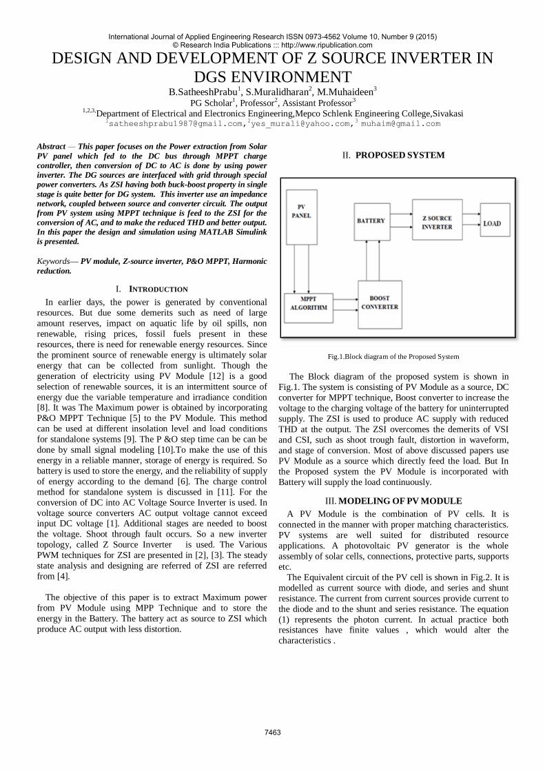
Fig.1.Block diagram of the Proposed System
The Block diagram of the proposed system is shown in
Fig.1. The system is consisting of PV Module as a source, DC
converter for MPPT technique, Boost converter to increase the
voltage to the charging voltage of the battery for uninterrupted
supply. The ZSI is used to produce AC supply with reduced
THD at the output. The ZSI overcomes the demerits of VSI
and CSI, such as shoot trough fault, distortion in waveform,
and stage of conversion. Most of above discussed papers use
PV Module as a source which directly feed the load. But In
the Proposed system the PV Module is incorporated with
Battery will supply the load continuously.
III. MODELING OF PV MODULE
A PV Module is the combination of PV cells. It is
connected in the manner with proper matching characteristics.
PV systems are well suited for distributed resource
applications. A photovoltaic PV generator is the whole
assembly of solar cells, connections, protective parts, supports
etc.
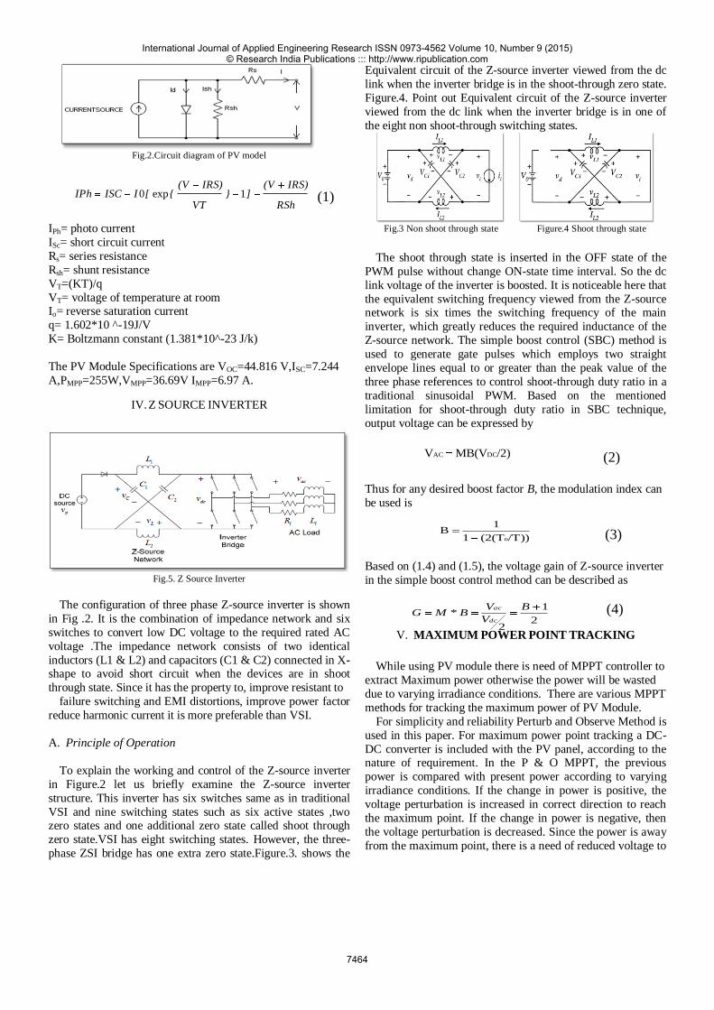
The Equivalent circuit of the PV cell is shown in Fig.2. It is
modelled as current source with diode, and series and shunt
resistance. The current from current sources provide current to
the diode and to the shunt and series resistance. The equation
(1) represents the photon current. In actual practice both resistances have finite values , which would alter the
characteristics .
International Journal of Applied Engineering Research ISSN 0973-4562 Volume 10, Number 9 (2015)© Research India Publications ::: http://www.ripublication.com
7463
Page 2
Fig.2.Circuit diagram of PV model
(1)
IPh= photo current
ISc= short circuit current
Rs= series resistance
Rsh= shunt resistance
VT=(KT)/q
VT= voltage of temperature at room Io= reverse saturation current
q= 1.602*10 ^-19J/V
K= Boltzmann constant (1.381*10^-23 J/k)
The PV Module Specifications are VOC=44.816 V,ISC=7.244
A,PMPP=255W,VMPP=36.69V IMPP=6.97 A.
IV. Z SOURCE INVERTER
Fig.5. Z Source Inverter
The configuration of three phase Z-source inverter is shown
in Fig .2. It is the combination of impedance network and six
switches to convert low DC voltage to the required rated AC
voltage .The impedance network consists of two identical
inductors (L1 & L2) and capacitors (C1 & C2) connected in X-shape to avoid short circuit when the devices are in shoot
through state. Since it has the property to, improve resistant to
failure switching and EMI distortions, improve power factor
reduce harmonic current it is more preferable than VSI.
A. Principle of Operation
To explain the working and control of the Z-source inverter
in Figure.2 let us briefly examine the Z-source inverter
structure. This inverter has six switches same as in traditional
VSI and nine switching states such as six active states ,two zero states and one additional zero state called shoot through
zero state.VSI has eight switching states. However, the three-
phase ZSI bridge has one extra zero state.Figure.3. shows the
Equivalent circuit of the Z-source inverter viewed from the dc
link when the inverter bridge is in the shoot-through zero state.
Figure.4. Point out Equivalent circuit of the Z-source inverter
viewed from the dc link when the inverter bridge is in one of
the eight non shoot-through switching states.
Fig.3 Non shoot through state Figure.4 Shoot through state
The shoot through state is inserted in the OFF state of the
PWM pulse without change ON-state time interval. So the dc
link voltage of the inverter is boosted. It is noticeable here that
the equivalent switching frequency viewed from the Z-source network is six times the switching frequency of the main
inverter, which greatly reduces the required inductance of the
Z-source network. The simple boost control (SBC) method is
used to generate gate pulses which employs two straight
envelope lines equal to or greater than the peak value of the
three phase references to control shoot-through duty ratio in a
traditional sinusoidal PWM. Based on the mentioned
limitation for shoot-through duty ratio in SBC technique,
output voltage can be expressed by
/2)MB(VV DCAC (2)
Thus for any desired boost factor B, the modulation index can
be used is
(3)
Based on (1.4) and (1.5), the voltage gain of Z-source inverter
in the simple boost control method can be described as
(4)
V. MAXIMUM POWER POINT TRACKING
While using PV module there is need of MPPT controller to
extract Maximum power otherwise the power will be wasted
due to varying irradiance conditions. There are various MPPT
methods for tracking the maximum power of PV Module.
For simplicity and reliability Perturb and Observe Method is
used in this paper. For maximum power point tracking a DC-
DC converter is included with the PV panel, according to the nature of requirement. In the P & O MPPT, the previous
power is compared with present power according to varying
irradiance conditions. If the change in power is positive, the
voltage perturbation is increased in correct direction to reach
the maximum point. If the change in power is negative, then
the voltage perturbation is decreased. Since the power is away
from the maximum point, there is a need of reduced voltage to
RSh
IRS)(V]}
VT
IRS)(V{[IISCIPh 1exp0
/T))(2(T1
1B
o
2
1
2
*B
V
VBMG
dc
ac
International Journal of Applied Engineering Research ISSN 0973-4562 Volume 10, Number 9 (2015)© Research India Publications ::: http://www.ripublication.com
7464
Page 3
reach the maximum power point. When the change in power
is zero, then the maximum power point is achieved. The
power at this point is denoted as PMPP and voltage and current
as VMPP and IMPP. This operation is shown as flowchart in
Fig.6.
Fig.6. Flow chart of P&O Method
VI. SIMULATION RESULTS
A. Simulation of ZSI
Fig.7. Simulation waveform of Z source inverter
In the proposed Z Source inverter designed for, the input
Es=48V,Vac=415V,L1=L2=1.103mH,C1=C2=215.50µF,
Modulation Index M=0.51, Duty cycle (Ds)=0.49.Fig.7.
shows the simulation waveform of Z Source inverter.The RL
load is connected to the output of the Inverter. The Gating
signals to the Inverter switching sircuit is applied with PWM generated with Simple Boost Control Technique. The first
waveform decribes the voltage across the Impedance Network
which attains the steady state gradually. The second waveform
explains the output voltage across the Inverter. The third
waveform explains the output current in the Inverter with RL
Load. It is in sinusoidal shape with 5% ripple.
B. Simulation of MPPT
The waveform in Fig.8.shows the Maximum power of PV.
The first waveform shows the duty cycle obtained from the
MPPT Technique is compared with carrier triangular signal
which is at 50 KHz. The duty cycle acts as reference signal to carrier wave to PWM signal. This signal is applied as gating
signal for boost converter switch. According to the applied
pulse the output of converter obtained at maximum power.
The third waveform shows power profile of PV Module. The
power is constant when it reaches the Maximum power. The
Table 1 shows the comparison of Max power with Specified
Power of PV and nearly Equal. In the specification 255 W is
given, by using P & O MPPT algorithm the Maximum power
is reached at 255 W. The Voltage (VPV) and Current (IPV) also
nearly as the given.
Fig.8. Simulation of Maximum power of PV
TABLE 1
COMPARISION OF MAXIMUM POWER
DESCRIPTION DESIGNED
PARAMETE
R VALUE
PARAMETE
R VALUE
ACHIEVED
VMPP 36.838 V 36.09 V
IMPP 6.925 A 7.079 V
PMPP 255 W 255 W
C.SIMULATION OF PV WITH MPPT & BATTERY
CHARGING CIRCUIT
International Journal of Applied Engineering Research ISSN 0973-4562 Volume 10, Number 9 (2015)© Research India Publications ::: http://www.ripublication.com
7465
Page 4
Fig.9. Simulation of PV with MPPT and Battery charging circuit
Fig.10.Simulation of charge controller circuit
The Fig.9.shows the simulation of PV interfaced with
MPPT and the output of the MPPT converter is connected to
the battery through boost converter. The rating of the battery
used is 48V, 125Ah. Lead acid battery type is used as battery
due to good high-rate performance, Good float
service, and Easy state-of-charge indication. Good
charge retention for intermittent charge. The
battery is charged through Battery charge controller. The
simulation of battery charge controller is shown in Figure.9.
In the simulation the voltage (VPV) and the Current (IPV) is fed
to MPPT block, to track Maximum power. The duty cycle
from MPPT block is fed as gating signal to the MPPT
converter. The output of the converter is given to the boost
converter which is used to charge the battery (48V, 125Ah) through charge controller. The Fig.10shows simulation of
battery charge controller consists of charge controller block
with current controller and selector switch block. Charge
controller block is designed with Matlab coding. The
Parameters of Boost converter are Vin=36V, Vout=48V,
L=67.49µH,C=216.67µF, Duty Cycle(D)=32.5.
In the Fig.11, the battery charging profile is shown. The
voltage from MPPT converter is sufficient to charge the
battery. So a boost converter is used for increase the voltage to
a level to charge the battery with the help of charge controller.
The charge controller is used charge the battery in constant
voltage method. The reference current is set according capacity and the voltage. In the simulation the first one shows
the state of charge (SOC) of the battery. While charging the
current gradually increases and attain the steady state is shown
in second part. The voltage of the battery charges to steady
state slowly according to the current charging. The battery is
charged through a charge controller. There is also the
indication for fully charged condition, and the battery is
isolated from the charger when it is charged. The reference
current is used maintain the current for charging.
Fig.11. Simulation charging battery profile
D. SIMULATION OF PV WITH ZSI
Fig.12.Simulation of PV with ZSI in Open loop
In Fig.12 shows the open loop control of PV with ZSI. Here
the PV with MPPT converter is created as block called PV
panel and MPPT and battery with boost converter is integrated
in the battery block. Since the current from PV panel is not
sufficient to meet the ZSI with load, its voltage is stored in
battery which has the rating 48V, 125Ah. While connecting this battery with ZSI it can supply the required current.
The PWM method for inverter is SBC Technique with
switching frequency in 10 KHz. It is created as a block and
fed as gating signals to the switches of the inverter. The
International Journal of Applied Engineering Research ISSN 0973-4562 Volume 10, Number 9 (2015)© Research India Publications ::: http://www.ripublication.com
7466
Page 5
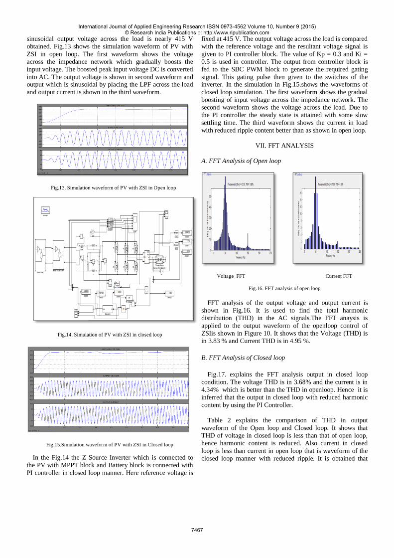
sinusoidal output voltage across the load is nearly 415 V
obtained. Fig.13 shows the simulation waveform of PV with
ZSI in open loop. The first waveform shows the voltage
across the impedance network which gradually boosts the
input voltage. The boosted peak input voltage DC is converted
into AC. The output voltage is shown in second waveform and output which is sinusoidal by placing the LPF across the load
and output current is shown in the third waveform.
Fig.13. Simulation waveform of PV with ZSI in Open loop
Fig.14. Simulation of PV with ZSI in closed loop
Fig.15.Simulation waveform of PV with ZSI in Closed loop
In the Fig.14 the Z Source Inverter which is connected to
the PV with MPPT block and Battery block is connected with
PI controller in closed loop manner. Here reference voltage is
fixed at 415 V. The output voltage across the load is compared
with the reference voltage and the resultant voltage signal is
given to PI controller block. The value of Kp = 0.3 and Ki =
0.5 is used in controller. The output from controller block is
fed to the SBC PWM block to generate the required gating
signal. This gating pulse then given to the switches of the inverter. In the simulation in Fig.15.shows the waveforms of
closed loop simulation. The first waveform shows the gradual
boosting of input voltage across the impedance network. The
second waveform shows the voltage across the load. Due to
the PI controller the steady state is attained with some slow
settling time. The third waveform shows the current in load
with reduced ripple content better than as shown in open loop.
VII. FFT ANALYSIS
A. FFT Analysis of Open loop
Voltage FFT Current FFT
Fig.16. FFT analysis of open loop
FFT analysis of the output voltage and output current is
shown in Fig.16. It is used to find the total harmonic
distribution (THD) in the AC signals.The FFT anaysis is
applied to the output waveform of the openloop control of
ZSIis shown in Figure 10. It shows that the Voltage (THD) is
in 3.83 % and Current THD is in 4.95 %.
B. FFT Analysis of Closed loop
Fig.17. explains the FFT analysis output in closed loop
condition. The voltage THD is in 3.68% and the current is in
4.34% which is better than the THD in openloop. Hence it is
inferred that the output in closed loop with reduced harmonic
content by using the PI Controller.
Table 2 explains the comparison of THD in output
waveform of the Open loop and Closed loop. It shows that
THD of voltage in closed loop is less than that of open loop,
hence harmonic content is reduced. Also current in closed
loop is less than current in open loop that is waveform of the
closed loop manner with reduced ripple. It is obtained that
International Journal of Applied Engineering Research ISSN 0973-4562 Volume 10, Number 9 (2015)© Research India Publications ::: http://www.ripublication.com
7467
Page 6
better THD in the closed loop condition. Thus the output is
analysed by FFT analysis.
Voltage FFT Current FFT
Fig.17 FFT analysis of closedloop
TABLE 2
COMPARISION OF THD
DESCRIPTION (V )THD (I )THD
ZSI OPENLOOP 3.83 4.95
ZSI CLOSED LOOP
3.68 4.34
VIII.CONCLUSION
In this Paper, the Power from PV system is connected to the
inverter through battery. Here Z source inverter (ZSI) is used,
for converting DC into AC. Because comparing with VSI and
CSI topologies, it is better. To extract the maximum power
Perturb and Observe MPP technique is used. The voltage across the PV system is boosted through boost converter and
stored in the battery with the help of battery charge controller.
The Maximum power is obtained by P&O method and it is
nearer to the required specification. The characteristics of PV
system are improved in this inverter topology. The Z Source
Inverter is directly connected to the Battery. The Battery acts
as source to Z Source Inverter. The control technique used in
ZSI is Simple Boost Control. The THD value of the output
waveform of the inverter is better in closed loop than open
loop of the inverter. The analysis can be extended to other
control techniques of source inverter in future.
REFERENCES
[1]. F. Z. Peng, ―Z-source inverter,‖ IEEE Trans. Ind. Appl.,
vol. 39, no. 2, pp. 504–510, Mar/Apr. 2003. [2]. Suresh l., G.R.S. Naga Kumar, and M.V.
Sudarsan―Modeling and Simulation of Z-source inverter, ―January 2012http://works.bepress.com/suresh_l/1
[3]. AnkitaPande, G.N Goyal, ―Comparison of Voltage gain of
different control methods Z Source Inverter,‖ International Journal of Engineering Research and Applications (IJERA) ISSN: 2248-9622 International Conference on Industrial Automation and Computing (ICIAC- 12-13th April 2014)
[4]. SumedhaRajakaruna, Senior Member, IEEE, and Laksumana Jayawickrama ―Steady-State Analysis and Designing Impedance Network of Z-Source Inverters‖ IEEE transactions on industrial electronics, vol. 57, no. 7,
July 2010. [5]. C.Nagarajan and M.Madheswaran - ‗Experimental
verification and stability state space analysis of CLL-T Series Parallel Resonant Converter‘ - Journal of Electrical Engineering, Vol.63 (6), pp.365-372, Dec.2012.
[6]. Nicola Femia, Member, IEEE, Giovanni Petrone, Giovanni Spagnuolo, Member, IEEE, and Massimo Vitelli ―Optimization of perturb and observe maximum power point tracking method,‖ IEEE Trans. Power Electron., vol.
20, no. 4, pp. 963–973, Jul. 2005. [7]. E. Koutroulis and K. Kazantzakis, ―Novel battery charging
regulation system for photovoltaic applications,‖ Proc. Inst. Elect. Eng.—Elect. Power Appl., vol. 151, no. 2, pp. 191–197, Mar. 2004
[8]. C.Nagarajan and M.Madheswaran - ‗Performance Analysis of LCL-T Resonant Converter with Fuzzy/PID Using State Space Analysis‘- Springer, Electrical Engineering, Vol.93
(3), pp.167-178, September 2011. [9]. Liqiang yang, Dongyuanqiu, bozhang and Guidongzhang,
―A high performance z source inverter with low capacitor voltage stress and small inductance‖ IEEE16-20, March2014.
[10]. R.Chedid, R.Tajeddine, F. Chaaban, R. Ghajar,―Modeling and Simulation of PV Arrays under Varying Conditions‖ 17th IEEE Mediterranean electro technical conference,
Beirut, Lebanon, 13-16 April 2014. [11]. C.Nagarajan and M.Madheswaran - ‗DSP Based Fuzzy
Controller for Series Parallel Resonant converter‘- Springer, Frontiers of Electrical and Electronic Engineering, Vol. 7(4), pp. 438-446, Dec.12.
[12]. Z. Jiang and R. A. Dougal, ―Multiobjective MPPT/charging controller for standalone PV power systems under different insolation and load conditions,‖ in
Conf. Rec. IEEE IAS Annu. Meeting, 2004, pp. 1154– 1160
[13]. C.Nagarajan and M.Madheswaran - ‗Experimental Study and steady state stability analysis of CLL-T Series Parallel Resonant Converter with Fuzzy controller using State Space Analysis‘- Iranian Journal of Electrical & Electronic Engineering, Vol.8 (3), pp.259-267, September 2012.
[14]. M. Sokolov, T. C. Green, P. D. Mitcheson, and D. Shmilovitz, ―Small signal model of photovoltaic power
converter for selection of perturb and observe algorithm step time,‖ in Proc. 14th Eur. Conf. Power Electron.Appl., Sep. 2011, pp. 1–5.
International Journal of Applied Engineering Research ISSN 0973-4562 Volume 10, Number 9 (2015)© Research India Publications ::: http://www.ripublication.com
7468