56
Karl Klang Simon Torstenson June 14, 2011 * Department of Energy and Environment Division of Electric Power Engineering CHALMERS UNIVERSITY OF TECHNOLOGY
Design and evaluation of a 1kW DC/DC- converter for contactless power transfer
DC/DC-converter utilizing a rotating transformer in an environmentdemanding high duty cycle and low voltage drops
Master of Science Thesis
Karl KlangSimon Torstenson
June 14, 2011
∗Department of Energy and EnvironmentDivision of Electric Power EngineeringCHALMERS UNIVERSITY OF TECHNOLOGY

Abstract
The concept of contactless transfer of power to rotating sensors have long been a desired fea-ture. Today the technology relied upon to supply such moving parts with power is slip rings.While being a well proven technology, slip rings are subject to wear and this in turn results in arelatively high maintenence frequency.
This master thesis deals with the design and evaluation of a 1kW DC/DC-converter. Thepurpose of this DC/DC-converter is to be used together with a rotating transformer in order toattain a contactless transfer of power for rotating sensors. The inverter part of the converteruses a full bridge topology. For the rectifier side, two different aspects are investigated andevaluated, diode rectifier bridges versus synchronous MOSFET rectifier bridges as well as theuse of center-tap configuration of the transformer versus a single secondary winding.
The resulting DC/DC-converter is a full bridge inverter with n-channel MOSFETs paralleledtwo and two. The transformer is connected with a single secondary winding (2:4 turns ratio)resulting in a total leakage inductance of 140nH and an effective maximum duty cycle of 97% ata switching frequency of 55kHz. The final rectifier used is a full bridge self-driven synchronousMOSFET rectifier, utilizing the secondary side of the transformer for gate signals. With aninput of 450W at 28V the converter reaches an efficiency of 94,4%, with the majority of the lossoriginating in the MOSFET’s switching and conduction of the inverter.
ii

Acknowledgements
This thesis would not have been possible without all the support given to us by our supervisorTorsten Nilsson at SAAB Electronic Defence system, EDS.
We also owe our gratitude for the great deal of support and knowledgible assistance from TordLinder and our main supervisor Daniel Dermark at SAAB EDS.
iii

Contents
1 Introduction 1
1.1 Problem background . . . . . . . . . . . . . . . . . . . . . . . . . . . . . . . 11.2 Previous work . . . . . . . . . . . . . . . . . . . . . . . . . . . . . . . . . . . 11.3 Purpose . . . . . . . . . . . . . . . . . . . . . . . . . . . . . . . . . . . . . . 21.4 Delimitations . . . . . . . . . . . . . . . . . . . . . . . . . . . . . . . . . . . 2
2 Technical background 3
2.1 Inverter . . . . . . . . . . . . . . . . . . . . . . . . . . . . . . . . . . . . . . 32.1.1 Switching . . . . . . . . . . . . . . . . . . . . . . . . . . . . . . . . . 32.1.2 Switching scheme . . . . . . . . . . . . . . . . . . . . . . . . . . . . 42.1.3 Duty cycle loss of the inverter . . . . . . . . . . . . . . . . . . . . . . 7
2.2 Rotating transformer . . . . . . . . . . . . . . . . . . . . . . . . . . . . . . . 82.2.1 Core loss - Hysteresis loss . . . . . . . . . . . . . . . . . . . . . . . . 82.2.2 Magnetizing inductance . . . . . . . . . . . . . . . . . . . . . . . . . 102.2.3 Leakage inductance . . . . . . . . . . . . . . . . . . . . . . . . . . . . 102.2.4 Winding resistance considerations . . . . . . . . . . . . . . . . . . . . 11
2.3 Rectifier . . . . . . . . . . . . . . . . . . . . . . . . . . . . . . . . . . . . . . 112.3.1 Full wave diode rectifier - Single secondary winding . . . . . . . . . . 122.3.2 Full wave diode rectifier - Center-tap on secondary winding . . . . . . 132.3.3 Self-driven synchronous rectifier - Center-tap on secondary winding . . 142.3.4 Self-driven synchronous rectifier - Single secondary winding (H-bridge
rectifier) . . . . . . . . . . . . . . . . . . . . . . . . . . . . . . . . . . 152.4 Snubber . . . . . . . . . . . . . . . . . . . . . . . . . . . . . . . . . . . . . . 162.5 MOSFET theory . . . . . . . . . . . . . . . . . . . . . . . . . . . . . . . . . 19
2.5.1 MOSFET intrinsic body diode . . . . . . . . . . . . . . . . . . . . . . 192.5.2 MOSFET switching characteristic . . . . . . . . . . . . . . . . . . . . 202.5.3 MOSFET power losses . . . . . . . . . . . . . . . . . . . . . . . . . . 23
3 Measurements and calculations 24
3.1 Measured duty cycle loss . . . . . . . . . . . . . . . . . . . . . . . . . . . . . 263.1.1 Influence on the total leakage inductance caused by conductors . . . . . 273.1.2 Synchronous rectification and effective duty cycle . . . . . . . . . . . . 29
3.2 Full bridge inverter losses . . . . . . . . . . . . . . . . . . . . . . . . . . . . . 303.2.1 Original full bridge inverter - Old MOSFETs . . . . . . . . . . . . . . 303.2.2 Improved full bridge inverter - New MOSFETs . . . . . . . . . . . . . 33
3.3 RotatingTransformer effects . . . . . . . . . . . . . . . . . . . . . . . . . . . 36
iv

3.4 Rectifier voltage - and power loss . . . . . . . . . . . . . . . . . . . . . . . . . 383.4.1 Measurements on the full wave diode rectifier - Single secondary winding 383.4.2 Measurements on the full wave diode rectifier - Center-tap on secondary
winding . . . . . . . . . . . . . . . . . . . . . . . . . . . . . . . . . . 393.4.3 Measurements on the self-driven synchronous rectifier - center-tap on
secondary transformer winding . . . . . . . . . . . . . . . . . . . . . . 403.4.4 Measurements on the self-driven synchronous rectifier - single secondary
transformer winding . . . . . . . . . . . . . . . . . . . . . . . . . . . 413.5 Snubber design . . . . . . . . . . . . . . . . . . . . . . . . . . . . . . . . . . 433.6 Output filter design . . . . . . . . . . . . . . . . . . . . . . . . . . . . . . . . 43
4 Conclusion 46
4.1 Results and discussion . . . . . . . . . . . . . . . . . . . . . . . . . . . . . . 464.1.1 Inverter . . . . . . . . . . . . . . . . . . . . . . . . . . . . . . . . . . 464.1.2 Transformer . . . . . . . . . . . . . . . . . . . . . . . . . . . . . . . . 474.1.3 Center-tap . . . . . . . . . . . . . . . . . . . . . . . . . . . . . . . . . 474.1.4 Rectifier . . . . . . . . . . . . . . . . . . . . . . . . . . . . . . . . . . 484.1.5 Influence on the leakage inductance caused by the switching frequency 49
4.2 Future work . . . . . . . . . . . . . . . . . . . . . . . . . . . . . . . . . . . . 50
5 References 51
v

1 Introduction
1.1 Problem background
In today’s radar systems the rotating antenna is provided with power via slip rings and rotatingjoints. Due to extreme demands on electro magnetic compatibility, EMC, introduced by radiocommunication etc, around the antenna, these mechanical parts are highly complex and proneto be in need of maintenance. The major issue with this solution is, apart from being a com-plex piece of mechanics which demands very specific knowledge, the fact that the wear leadto a relatively high maintenance frequency. An alternate method of transfering power could beusing an inductive coupling via a rotating transformer which then provde a contactless and thusfriction-less solution. In the system in question the antenna electronics requires a bus voltage of56V DC which could potentially be supplied from the already available 28V DC in static partsof the radar system, if DC-transformation was applied.
1.2 Previous work
A great deal of research in this subject, with different solution of the problems evolving fromthis scenario. The main issues of this research being to keep the losses as well as the EMI low,e.g. (Papastergiou and Macpherson 2007). A common conclusion is that a fairly high frequencyshould be used in order to reduce the filter losses, however few texts deal with the issue of highduty cycle demand. In order to keep frequency high the switching usually has to be done in a lowloss and low electro magnetic interference, EMI, manner. There are two aspects involved in thisprocess. First the switching losses, introduced by the current through the switch and the voltageover the switch being non-zero simultaneously during the switching, should be reduced. Thisis normally done by forcing the switching to occur during zero-voltage (ZVS) or zero-current(ZCS) conditions. A great number of papers have been published in this field and the numberof solutions to the problem is steadily growing. The main idea however is to cleverly use thedifferent paths of the circuit in order to use the natural commutations of for instance diodesto perform the switching at appropriate times or by using a controlled resonance and time theswitching according to that. While doing this the EMI should be limited by either shielding orlimiting the di/dt- and dv/dt- properties of elements in the circuit.
1

1.3 Purpose
The purpose of this thesis is to design and evaluate a building block, prototype of a completeDC/DC converter, using partly already available converter parts.
The main purpose is to perform an analysis of the feasibility of using the rotating transformerin this type of system and to construct a technical specification of the requirements for such asystem. The DC/DC converter should have a working range of 500W to 1000W and give anoutput voltage of between 48V and 60V, keeping as close to 56V as possible and at the sametime attain a high efficiency.
1.4 Delimitations
The only aspect of the transformer investigated in this thesis is the use of different windingconfigurations. The converter should utilize hard switching, i.e. not purposely working towardssoft-switching. The output voltage waveform, pre-filter may not rise above 60V. This adds alimitation on the transformer winding ratio that is possible to use for the transformer. Sincethe average output voltage desired (56V) is fairly close to this maximum allowed value (60V),this also means that a high duty ratio, as close to 100% as possible, is required. This, dueto the fact that a lower current would lead to a reduction of inductive duty cycle loss, resultin an unexpected duty cycle increase. The converter should ideally not require any controlsignals from external systems in order to operate efficiently. The thesis should work with apredetermined transformer, with 4 turns on primary and secondary side, giving a very limitednumber of winding configuration options. The 56V DC on the secondary side can be allowedto vary slightly, meaning that the converter does not need to have a primary to secondary sidefeedback control.
2

2 Technical background
2.1 Inverter
One of the main factors regarding the use of a rotating transformer compared to the conventionalsystems is the low magnetizing inductance introduced by the existence of a substantial air gap.This air gap has to be there in order to allow rotation of the transformer with little or close tozero friction. The resulting magnetizing current, that will always flow through the primary sideregardless of the loading level, will result in increased conduction losses.
In situations like this, where the primary side current is of high importance, a common inverteris the phase-shifted full bridge inverter, PSFB. In the PSFB an auxiliary circuit is used in orderto introduce the necessary energy needed to discharge a parallel capacitance and by the use ofthat attain zero-voltage transitions of the switches.
At these kinds of power levels, full bridge configurations are popular for several reasonsbut mostly due to their bidirectional quality, meaning it provides the full input voltage in bothpositive and negative direction, as opposed to half the input voltage, which would be the caseof a unidirectional inverter. Having higher voltage means lower current and thus decreasedconduction losses.
When it comes to the choice of switch type, in this thesis MOSFETs are considered. Greatlydue to good high-frequency characteristics and possibility of low conduction losses but alsodue to the unacceptable voltage drop of for instance IGBTs, which otherwise might have beenconsidered as an alternative.
2.1.1 Switching
Using fixed duty cycle, allows for an optimization of the drive circuit components for this spe-cific duty cycle. Due to certain degrees of freedom introduced by the application specification(there is a high performance DC/DC converter on the input of the load) there is no need forfeedback control, i.e. the converter should provide a fix ratio between input and output, regard-less of variation in load- and input- voltage. To reduce output ripple one can either increase thesize of the output filter or increase the frequency. Commonly one would prefer to increase thefrequency to minimize losses. In order to maintain a fairly high frequency it becomes highlyrelevant that the losses involved with this do not go out of hand and the benefits of the higherfrequency does not get outweighed.
Traditionally this might be achieved by performing soft-switching and thus removing most ofthe switching losses, however the aim of this thesis is to provide a working model and not to addextra complexity.
3

2.1.2 Switching scheme
The inverter considered in this thesis is a full bridge inverter, based on an existing PSFB inverter,where the phase shift is driven to be as close to 100% as possible. This inverter is designed fora higher voltage and power level but approximately the same load current, resulting in similardemands on cooling and thus mounting, making it a suitable starting point. The term phaseshifted full bridge relates to a control scheme where both legs are separately driven to a dutyratio very close to 50% and then phase shifted against each other (Andreycak 1997). Other thanthe 180 degrees shift between the two legs’ waveforms there is also a delay between the turn offof one transistor and the turn on of the other one in the same leg. Primarily this ensure that thefull bridge doesn’t suffer from current shoot through, which it otherwise would have issues withat time periods where both the upper and the lower transistor in the same leg are open, i.e. thesupply is short circuited. The main point about phase shifted control in comparison with usingconventional pulse width modulation (pwm) waveforms is the possibility to not only control theduty cycle but also add some degree of control of the switching losses. In the proposed fullbridge, it is not possible to reach quite 100% phase shift, but one can get very close, around99%. The basic switching waveforms are shown in Figure 2.1.
Figure 2.1: Switching waveforms of the proposed phase shifted full bridge inverter (Gate-sourcesignals).
4

The resulting switching scheme is described in Figure 2.2.
(a) t1-t2(b) t2-t3
(c) t3-t4 (d) t4-t5
(e) t5-t6 (f) t6-t7
Figure 2.2: Switching schedule of the phase shifted full bridge inverter.
The switching schedule illustrated in Figure 2.2 is broken down into time intervals and ex-plained below.
t1-t2 At this point, the load current flows in the positive reference direction through SW1 andSW4, as shown in Figure 2.2a. Power is being delivered to the the load and the overall fullbridge is in an on-state. At t2, SW4 is turned off.
5

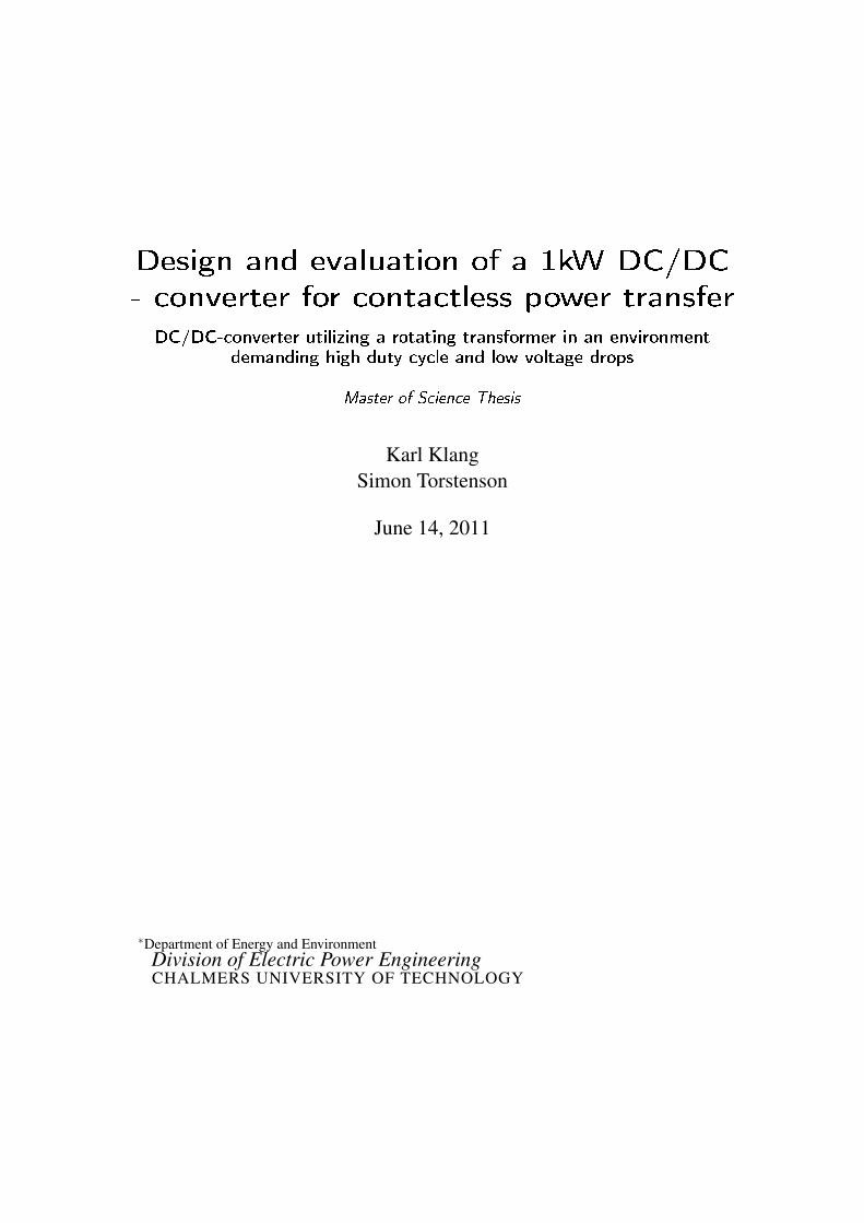
t2-t3 The case of Figure 2.2b. During the turn-off of SW4, its current commutates to the bodydiode of SW3. This interval is the part of the dead-time controlled by the phase shifted gate-pulse control and often referred to as the freewheeling interval. With the control used in thisthesis, the freewheeling intervals last for approximately 40 ns, according to Figure 2.3 below.
t3-t4 At t3 SW1 is turned off and the decreasing current through it, if any, commutates to thebody diode of SW2, Figure 2.2c. The description of this stage depends on the load conditionand the inductance of the converter circuit. If the full load current reaches zero within the 40 nsof period t2-t3, the current will simply be zero until t4. If not, the time between t3 and t4 is setby the time it takes for the current to reach zero at full, reversed supply voltage.
t4-t5 At t4 the case of Figure 2.2d starts as the current has reversed and is actively driven inthe negative reference direction through SW2 and SW3, which are turned on (SW2 40ns afterSW3). Similar to period t1-t2 this goes on until t5 where SW3 is turned off.
t5-t6 As in the other half period, the current previously in the right leg MOSFET commutatesto the body diode of the opposite transistor in the same leg, in this case the current through SW3commutates to the body diode of SW4, as shown in Figure 2.2e. After another 40 ns delay t6 isreached.
t6-t7 At t6 SW2 is turned off, while SW2 is turned on and the current through SW2 commu-tates to the body diode of SW1. This stage ends at t7, where the case of Figure 2.2f has begun.The current reversal is completed and SW1 and SW4 is turned on (SW1 40 ns after SW4) as theswitching scheme is repeated from t1.
6
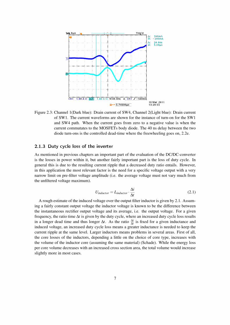
Figure 2.3: Channel 1(Dark blue): Drain current of SW4, Channel 2(Light blue): Drain currentof SW1. The current waveforms are shown for the instance of turn-on for the SW1and SW4 path. When the current goes from zero to a negative value is when thecurrent commutates to the MOSFETs body diode. The 40 ns delay between the twodiode turn-ons is the controlled dead-time where the freewheeling goes on, 2.2e.
2.1.3 Duty cycle loss of the inverter
As mentioned in previous chapters an important part of the evaluation of the DC/DC-converteris the losses in power within it, but another fairly important part is the loss of duty cycle. Ingeneral this is due to the resulting current ripple that a decreased duty ratio entails. However,in this application the most relevant factor is the need for a specific voltage output with a verynarrow limit on pre-filter voltage amplitude (i.e. the average voltage must not vary much fromthe unfiltered voltage maximum).
Uinductor = Linductor ·∆i∆t
(2.1)
A rough estimate of the induced voltage over the output filter inductor is given by 2.1. Assum-ing a fairly constant output voltage the inductor voltage is known to be the difference betweenthe instantaneous rectifier output voltage and its average, i.e. the output voltage. For a givenfrequency, the ratio time ∆t is given by the duty cycle, where an increased duty cycle loss resultsin a longer dead time and thus longer ∆t. As the ratio ∆i
∆t is fixed for a given inductance andinduced voltage, an increased duty cycle loss means a greater inductance is needed to keep thecurrent ripple at the same level. Larger inductors means problems in several areas. First of all,the core losses of the inductors, depending a little on the choice of core type, increases withthe volume of the inductor core (assuming the same material) (Schade). While the energy lossper core volume decreases with an increased cross section area, the total volume would increaseslightly more in most cases.
7

The other factor is slightly more obvious, the size and weight of the complete converter. Forthe sake of this thesis the duty cycle is, as mentioned, not only important due to the increasedfilter losses a poor duty cycle ratio would entail, but also by the fact that the application it ismeant for requires a specific range of voltage input/output ratios.
2.2 Rotating transformer
There are three factors of the transformer needed to be investigated for this thesis. First the mag-netizing inductance of the transformer, as this determines the amount of core loss to be expectedand secondly the leakage inductance of the transformer and finally the winding resistance. Thefact that the transformer is a rotating transformer does not actually affect this thesis very muchsince the choice of transformer is one of the already available delimitations and thus no designapart from the choice of winding configuration is possible. One factor needed to be considered,however, is the effect of the transformer’s air gap. In an optimized none-moving transformer,the air gap would be reduced, but in this case it is needed to allow for friction free movement.
2.2.1 Core loss - Hysteresis loss
When looking at the losses of a transformer there are, as mentioned above, several aspects thatshould be considered. First there is the obvious part of resistive losses, caused by traditionalresistive heating by current in the conductor windings. While this has a frequency dependenceintroduced by the induced eddy currents, the electric power loss is still caused by simply conduc-tion heating. The second and in this case more important part is the magnetizing losses withinthe core.
8

Every time the magnetic flux is reversed within the core, the magnetic dipoles of the materialalign themselves with the field causing a certain amount of loss equal to the energy requiredto move the dipoles. This is often illustrated by a hysteresis, like the one in Figure 2.4, thusexplaining the name, hysteresis loss.
Figure 2.4: Magnetic hysteresis, depicting the energy loss involved in reversing the polarity of acertain magnetic material.
The figure shows the magnetic flux density, B, inside the core versus the magnetic field ap-plied, i.e. the magnetizing current. If a magnetic field is applied and then removed, the energyused to align the dipoles within the core material is stored and must be removed in order to returnthe flux to zero. Every time the polarity of the current in the transformer changes, this storedenergy is removed at the cost of the curve shifting, as extra magnetic force is required to changethe magnetic flux. The energy loss involved in every switching period is illustrated by the areaenclosed by this hysteresis.
9

2.2.2 Magnetizing inductance
In the prestudy of the rotating transformer, the magnetizing inductance has been measured un-der certain conditions with the use of no-load tests. At 50.3kHz, the magnetizing inductanceis found to be approximately 20.25µH in a 1:4 winding ratio connection. In this thesis, bothcenter-tap configuration, where two seperate windings with a common center-point is used onthe secondary, as well as single secondary winding is to be considered. The values should there-fore be known for a winding ratio of 1:2:2 and 2:4. Depending on how good an approximationof the inductance one needs, complicated formulas to calculate more or less accurate values,depending on form factors etc can be used. However in this case, due to the limitations at hand,the only thing interesting is the approximate ratio between these two cases. As such, an adequateapproximation can be found by simply stating that the magnetizing inductance is proportional tothe number of primary windings, squared. I.e. if the primary windings change from 1 to 2, themagnetizing inductance increases approximately with a factor of 4. Further, in the prestudy, thecore losses are found to be approximately 27.3W for the 1:2:2 configuration and 2.73W for the2:4 configuration in theory. The approximated values are presented in Table 2.1.
2.2.3 Leakage inductance
An other important factor is, as mentioned above, the leakage inductance of the transformer andthe rest of the circuit. This is not so much related to losses as in the case of the magnetizinginductance but in current reversal speed. The speed at which the current can be reversed isdirectly related to how high switching frequency can be used in order to achieve an adequateduty ratio. The time it takes to reverse the current results in a forced dead-time and the higherthe frequency, the more it affects the possible duty ratio. In the same prestudy of the transformer,measurements of the transformer leakage inductance at 52kHz can be found to be approximately500nH at four primary turns. With the same reasoning as with the magnetizing inductance, theleakage inductance values at ratios of 1:2:2 and 2:4 becomes 31.25nH and 125nH respectively.The assumption here is that changing the winding configuration does not affect form factors aswell as mutual inductance between the two secondary windings. These result are also shown inTable 2.1.
Table 2.1: Theoretical transformer parameters. These are extrapolated using known values atdifferent winding configuration and very similar frequencies.
Center-tap Single secondary winding1:2:2 2:4
Magnetizing inductance 20.25µH 81µHLeakage inductance 31.25nH 125nH
Core loss 27.3W 2.73W
10

An easy way, to measure total leakage inductance of a circuit like this one, is to look at thecurrent induced dead time at the input of the rectifier part. With the current and voltage known,all that is needed is the dead time, in order to calculate the inductance according to:
Vin = Lleakage2 · Iin
Tdead−time⇒ Lleakage =
Vin ·Tdead−time
2 · Iin(2.2)
2.2.4 Winding resistance considerations
The transformer is designed in such a way that the winding resistance should be a very small partof the total impedance seen by the primary side, however it has not been completely optimized.As the resistance is subject to the skin effect at alternating currents, the skin depth is whatlimits the resistance. In a final winding design this would be accounted for to make sure, atthe frequency you want to use, the skin dept take up as big part of the complete winding cross-section as possible, but no more.
δ =
√2ρ
ωµ(2.3)
where:δ =the skin depthρ = resistivity of the conductorω = angular frequency of the alternating currentµ = absolute magnetic permeability of the conductor
In this transformer this fact is, however, merely pointed out but not designed for.
2.3 Rectier
When it comes to the rectification part of the converter, there are two aspects investigated inthis thesis. First the option to use a center-tap on the transformer secondary winding shouldbe investigated in terms of voltage drop, duty cycle and efficiency, where the positive aspectsshould be weighted against the negative. Secondly the possible benefits of using synchronousrectification should be investigated for two cases with and without a center-tap configuration onthe transformer secondary winding. As there is only a factor of two between the voltage on theprimary and secondary side, the voltage drop over the active components must still be kept wellbelow that of for instance IGBTs and also here MOSFETs are chosen as active components, i.e.for the synchronous rectifiers.
11
2.3.1 Full wave diode rectier - Single secondary winding
The single winding diode rectifier bridge is one of the most commonly used rectifiers in elec-tronic equipment. It is a full-wave rectifier, using four diodes to rectify alternating current andits set-up is illustrated in Figure 2.5.
Figure 2.5: Traditional four diode full wave diode rectifier for a single secondary transformerwinding. The blue and red lines/arrows show the two different current paths of therectifier.
When Vrecti f ier is positive, D3 and D2 are forward biased and the current starts to conductthrough them. At the same time, D1 and D4 becomes reversed biased, thus preventing thecurrent to flow through them. When Vrecti f ier changes polarity, it is the other way around. Thecurrent then flows through D1 and D4 while D2 and D3 are blocking and the output voltage willkeep the same polarity.
The main benefits using a diode bridge are its simplicity and the low design costs. The bigdisadvantage is on the other hand the voltage drops over each diode and the conduction lossesthat will arise.
12

2.3.2 Full wave diode rectier - Center-tap on secondary winding
The center-tapped full wave rectifier utilizes the two secondary windings of a transformer in away that only two diodes are needed in the rectifier (Figure 2.6).
Figure 2.6: Full wave diode rectifier with a center-tap on the secondary transformer winding.The blue and red lines/arrows show the two different current paths of the rectifier.
The number of turns for both windings on the secondary side is the same and the voltageacross each winding will thereby be the same. When Vrecti f ier is positive, D1 will be forwardbiased while D2 is blocking and the current will flow out from the dot on the first winding onthe secondary side. When the input voltage change polarity, D2 will be forward biased whileD1 is blocking, and the current will flow into the dot of the second winding on the secondaryside. Since this center-tapped full wave rectifier uses only two diodes, the voltage drop andconducting losses are lower than for the diode bridge, making it more suitable for low voltageand high current systems.
13
2.3.3 Self-driven synchronous rectier - Center-tap on secondary winding
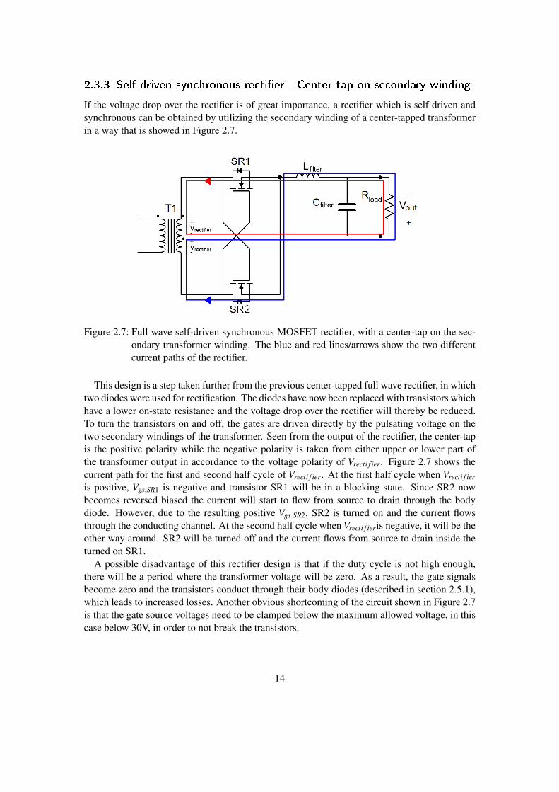
If the voltage drop over the rectifier is of great importance, a rectifier which is self driven andsynchronous can be obtained by utilizing the secondary winding of a center-tapped transformerin a way that is showed in Figure 2.7.
Figure 2.7: Full wave self-driven synchronous MOSFET rectifier, with a center-tap on the sec-ondary transformer winding. The blue and red lines/arrows show the two differentcurrent paths of the rectifier.
This design is a step taken further from the previous center-tapped full wave rectifier, in whichtwo diodes were used for rectification. The diodes have now been replaced with transistors whichhave a lower on-state resistance and the voltage drop over the rectifier will thereby be reduced.To turn the transistors on and off, the gates are driven directly by the pulsating voltage on thetwo secondary windings of the transformer. Seen from the output of the rectifier, the center-tapis the positive polarity while the negative polarity is taken from either upper or lower part ofthe transformer output in accordance to the voltage polarity of Vrecti f ier. Figure 2.7 shows thecurrent path for the first and second half cycle of Vrecti f ier. At the first half cycle when Vrecti f ier
is positive, Vgs,SR1 is negative and transistor SR1 will be in a blocking state. Since SR2 nowbecomes reversed biased the current will start to flow from source to drain through the bodydiode. However, due to the resulting positive Vgs.SR2, SR2 is turned on and the current flowsthrough the conducting channel. At the second half cycle when Vrecti f ieris negative, it will be theother way around. SR2 will be turned off and the current flows from source to drain inside theturned on SR1.
A possible disadvantage of this rectifier design is that if the duty cycle is not high enough,there will be a period where the transformer voltage will be zero. As a result, the gate signalsbecome zero and the transistors conduct through their body diodes (described in section 2.5.1),which leads to increased losses. Another obvious shortcoming of the circuit shown in Figure 2.7is that the gate source voltages need to be clamped below the maximum allowed voltage, in thiscase below 30V, in order to not break the transistors.
14

2.3.4 Self-driven synchronous rectier - Single secondary winding(H-bridge rectier)
If a center-tapped transformer is hard to achieve, the synchronous H-bridge rectifier is a goodchoice when the voltage drop of a diode is unacceptable. This rectifier can be seen as a fourdiode rectifier bridge, but with its diodes replaced with transistors. Due to the internal bodydiode of the MOSFET the transistor can only prevent current flowing in one direction (drain tosource). Hence, to prevent a possible short circuit in one of the legs of the H-bridge, it is of greatimportance that the transistors are oriented in the correct direction, see Figure 2.8.
Figure 2.8: Full wave self driven synchronous MOSFET rectifier, with a single secondary trans-former winding.
One of the differences between this one and the synchronous rectifier with a center-tap is thatit is not quite as easy to drive by directly using the transformer secondary winding, so it usuallyrequires a special connection in order to acquire gate drive signals.
The transistors here are N-channel enhancement MOSFETs and they have been connected insuch a way that they may only conduct in the reverse direction. This means that without gatedriver the rectifier would have the same operation as that of a diode bridge. However, turning thetransistors on by applying synchronous gate pulses to the transistor gates will allow the majorityof the current to start flowing through enhanced low resistance n-channel instead of the intrinsicbody diode. When Vrecti f ier is positive, the current will flow through SR3 and SR2 or SR1 andSR4 if Vrecti f ier is negative.
15

2.4 Snubber
There are many different types of snubbers, used for different situations. In the types of appli-cation regarded in this thesis, there are basically two groups of snubbers considered:
• Turn-off snubbers - Used to decrease the δV/δ t of the voltage between the drain and thesource of transistors in order to reduce the losses at turn-off of these transistors, throughzero - or lower than nominal voltage transition.
• Damping snubbers - Similar to the turn-off snubber but more focus on the damping co-efficient, in order to reduce ringing effects at inductive turn-off of currents through semi-conductor devices.
There is a certain issue regarding the time it takes to perform a switching, though for the MOS-FETs considered in this thesis with a switching time of approximately 50ns, this is not thegreatest source of power loss. A much greater issue at turn off comes from a phenomenon calledvoltage ringing. This effect is shown in Figure 2.9 and is cause by current, going through aninductance, being forced to change almost momentarily by a semiconductor device. Basicallythe voltage oscillates between the leakage inductance and the leakage capacitance of the circuit.
Figure 2.9: Oscilloscope plot of the drain-source voltage (green) and the drain current (blue) ofa primary side inverter MOSFET. As seen in the picture, when the current is turnedoff and the voltage rises, the voltage continues far beyond the off-state value only tolater on be slowly damped over time.
Two common methods of dealing with this is to either provide an alternate path for the currentto go and thus not interupt it instantaneously or to more directly reduce the δ I/δ t by the use ofsnubbers. Also here, there are many complex alternatives but the most common snubber is theRC snubber in which a resistor and a capacitor is put in parallel with the device being protected.
To further simplify the situation an even simpler, purely resistive snubber can be used toexplain the situation and derive a solution.
16

Breaking down the situation of the semiconductor device during turn-off, the equivalent sim-plified resonant tank described in Figure 2.10 can be used to illustrate the ringing effect, wherethe charge up of the capacitance induces a current in the inductance, which in turn dischargesthe capacitor and so on.
Figure 2.10: Very simple resonant tank depicting the equivalent situation of the drain-source ofthe semi conductor device at turn-off.
With simple voltage division, a transfer function from input to output can be found as in(Hagerman 1995):
H(s) =
(Rs · 1
sC
Rs +1
sC
)(
Rs · 1sC
Rs +1
sC
)+ sL
=
( 1LC
)s2 + s
(1
RsC
)+( 1
LC
) (2.4)
Where in the general second order response
2ζ ωn =1
RsC
and
ω2n =
1LC
with ωn being the natural oscillation frequency of the circuit in radians and ζ being the damp-ing coefficient. Thus the transfer function can be put in the general form
T (s) =ω2
n
s2 + s(2ζ ωn)+ω2n
(2.5)
.Finally the value of the snubber can be solved as
17

Rs =1
2ζ ωnC=
(1
2ζ
)√LC
(2.6)
In Figure 2.11 the response is shown for different values of the damping coefficient. The goalis to use enough damping to get the oscillations down, but not too much, since excessive dampingleads to unnecessary resistive loss. A common approach is to choose a damping coefficient of0.5 resulting in
Rs =
√LC
or as it is commonly referred to, the characteristic impedance of the circuit.Regarding the shape of the waveform this snubber would do a very effective job, however the
power dissipation of this snubber would be very high. Here the second part of the snubber designtakes in. After choosing a desired value of Rs to achieve the desired ζ a capacitor is connectedin series with it to greatly increase the DC-resistance of the snubber.
Replacing Rs in equation 2.4 with(
Rs +1
sCs
)the -3dB cutoff frequency is found and given by
fo =1
2πRsCs
To make sure the cut off frequency really passes through the snubber effortlessly a slightlylower frequency should be designed for, in order to achieve the damping desired. By choosingto design for a factor 2π lower frequency the capacitor value is given by
Cs ≈1
Rs fringing(2.7)
Figure 2.11: Step response of a general second order transfer function at different dampeningcoefficients ζ . At ζ =0.5 a good degree of dampening occurs without decreasingthe speed of the system very much.
18

2.5 MOSFET theory
The metal-oxide-semiconductor field effect transistor (MOSFET) is a gate charge controlledtransistor (Undeland 2003). It requires a positive gate-source voltage in order to charge up thegate to turn it on. It then creates a channel between its drain and source which can conductcurrent in either direction, depending on the drain-source voltage polarity. Since the MOSFETis a charge controlled device it is easy to control the speed at which it switches by addinggate driving circuits to control the current that flows into and out of the gate. It also has arelatively high possible switching speed, making it the preferred choice of transistor in manyhigh frequency applications.
The MOSFET transistor has a positive temperature coefficient which means that several unitscan be placed in parallel and thus decrease the total drain-source resistance Rds,on. When oneunit is conducting more current than the others, its temperature increases and thereby also thechannel resistance, thus making the current divide it self evenly among the transistors. However,with increased voltage blocking capabilities of the MOSFET, the conduction channel has to belonger, thus increasing its resistance (due to increased drain/drift region thickness). Thereforeit is often considered less suitable for high voltage applications, than other alternatives, such asIGBTs.
2.5.1 MOSFET intrinsic body diode
One important parasitic component in a MOSFET transistor is the BJT that emerges across thedrain and source contacts. With the body, drain and source of the MOSFET serving as base,collector and emitter respectively, the BJT might turn on if the voltage across the body andsource is high enough. Since this will destroy the device, the source and body are connectedtogether as a protection. As a result, there is instead an intrinsic diode formed inside the body-drain p-n junction of the MOSFET.
Figure 2.12: Schematic picture of a MOSFET transistor.
19

The diode can be observed in Figure 2.12 where it is connected between the drain and source,(in red) making it useful as a freewheeling diode in half- and full-bridge converters. On the leftside of Figure 2.12, the possible BJT transistor formed across the drain and source contacts isshown in red.
2.5.2 MOSFET switching characteristic
The switching characteristics of a MOSFET transistor can be explained in four steps where eachstep relates to a certain time interval of the total switch-on/off time. Starting with the turn-onsequence, the graphs in Figure 2.13 are theoretical representations of the gate current iG, gate-source voltage VGS, drain-source voltage VDS and drain current iD, in these time intervals.
Figure 2.13: Switching waveforms of a MOSFET transistor during an ideal turn-on.
20

The transistor can be modeled with equivalent circuits, which correspond to each interval, asshown in Figure 2.14. The current source with the parallel diode is the model of an inductiveload and Rg is an external gate resistance. The four steps during the turn-on are described below:
(a) Equivalent model of the MOSFET tran-sistor during time interval 1. The timeinterval corresponds to the time it takesto charge the gate up to the thresholdgate-source voltage.
(b) Equivalent model of the MOSFET tran-sistor during time interval 2. This inter-val is the interval during which the draincurrent rises from zero to the load thefull load current.
(c) Equivalent model of the MOSFETtransistor during time interval 3.The interval during which the drain-source voltage falls to zero after thedrain current has turned fully on.
(d) Equivalent model of the MOSFETtransistor during time interval 4.This interval corresponds to the timewhere the conduction channel furtherenhances to reduce the resistance.Parallel to this, the gate gate-sourcevoltage rises to the full gate-sourcevoltage of the gate drive circuit.
Figure 2.14: Equivalent models of the MOSFET during the different stages of its turn-on pro-cess.
21

1. The first interval (2.14a) is called the turn-on delay. The name is given due to that bothVDS and iD, are remaining unchanged. During this stage iG is primarily charging thegate-source capacitance Cgs, but there is also a small current flowing into the gate-draincapacitance Cgd , (also called the miller capacitance). VGS now appears to increase linearlyfrom zero to VGS(th), although it is in reality a part of an exponential curve with timeconstant τ1 = RG(Cgd1 +Cgs).
2. In the next interval (2.14b) iG continues to charge Cgd and Cgs, causing VGS to increaseabove VGS(th). At the same time, iD has started to increase and is doing so linearly withVGS. VDS remains constant until the current iD consist of the whole load current I0. Whenthis occurs, the free wheeling diode D f is no longer forward biased, thus not conducting,and VDS starts to decrease.
3. During the third interval (2.14c) VGS is clamped to VGS,I0 .The resulting plateau is charac-terized as the “Miller plateau”. With the drain current iD now being equal to I0 and theMOSFET operating in the active region, the gate current can do nothing other than dis-charging Cgd and thus decrease VGD. As a result, VDS will eventually drop to zero, as VDS
is the sum of VGS and VGD.
4. When both capacitances Cgs and Cgd are fully charged (2.14d), VGS will grow exponen-tially, with time constant τ2 = Rg(Cgd2 +Cgs), until it reaches the supplied gate voltageVGG.
A similar analytical approach which was used above for finding the turn-on switching waveformscan be used when finding the turn-off waveforms. The sequence in this case is the inverse ofthe stages during turn-on. However, the times during each interval may be different since theapplied gate voltage at turn-off can sometimes be set to minus VGG instead of zero. This is donein an effort to speed up the turn-off and is the case used for this thesis.
22
2.5.3 MOSFET power losses
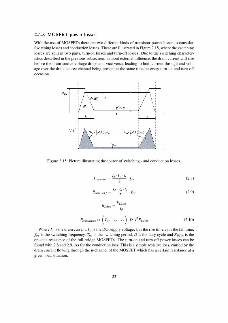
With the use of MOSFETs there are two different kinds of transistor power losses to consider.Switching losses and conduction losses. These are illustrated in Figure 2.15, where the switchinglosses are split in two parts, turn-on losses and turn-off losses. Due to the switching character-istics described in the previous subsection, without external influence, the drain current will risebefore the drain-source voltage drops and vice versa, leading to both current through and volt-age over the drain source channel being present at the same time, at every turn-on and turn-offoccasion.
Figure 2.15: Picture illustrating the source of switching - and conduction losses.
Pturn−on =Id ·Vd · tr
2· fsw (2.8)
Pturn−o f f =Id ·Vd · t f
2· fsw (2.9)
RDSon =VDSon
Id
Pconduction ≈(
Tsw− tr− t f
)·D · I2RDSon (2.10)
Where Id is the drain current, Vd is the DC-supply voltage, tr is the rise time, t f is the fall time,fsw is the switching frequency, Tsw is the switching period, D is the duty cycle and RDSon is theon-state resistance of the full-bridge MOSFETs. The turn-on and turn-off power losses can befound with 2.8 and 2.9. As for the conduction loss; This is a simple resistive loss, caused by thedrain current flowing through the n-channel of the MOSFET which has a certain resistance at agiven load situation.
23

3 Measurements and calculations
In the first part of the thesis upto the point where the second rectifier is applied (the center-tap2-diode rectifier bridge) the measurement euipment used is presented in Measurement setup 1:
• TDS220 - Oscilloscope, 2 channel digital
• Tektronix TCP202 - DC to 50MHz current probe
• Tektronix 1103 TekProbe Power Supply - Power supply for current probes when usedtogether with TDS220 (to prevent saturation of probe at DC-currents)
• Oltronix B40-1 - DC Power supply
• 2 x Isolation transformer
The connection setup is presented in Figure 3.1.
Figure 3.1: Blockdiagram of measurement setup, for the whole converter.
As can be seen in the picture, both the oscilloscope and the power supply is connected to thegrid via isolation transformers. This is done to solve issues with circulating ground signals (pri-marily 50Hz noise) and common mode disturbances, by providing separate ground potentials.
24

After the point where the inverter has stopped being considered, the equipment used is pre-sented in Measurement setup 2:
• TDS 3014B - Oscilloscope, 4channel digital
• Tektronix TCP202 - DC to 50MHz current probe
• Delta electronica SM7020-D - DC - Power supply
• 2 x Isolation transformer
In Figure 3.2 the actual connection set-up is shown.
Figure 3.2: Photograph of the actual converter.
25

3.1 Measured duty cycle loss
There are many sources of duty cycle loss in this circuit, but the single greatest one is theone caused by the commutation time, due to the circuit inductance. When a reverse voltage isapplied at the output of the full bridge the current takes some time to change in the full circuit.This phenomenon is shown in Figure 3.3.
Figure 3.3: Ch1 (Blue) is here the drain current of one of 4 parallel MOSFETs, i.e. a forthof the total primary side drain current. Ch3 (purple) is the output of the full wavediode rectifier. While the current rises linearly (due to the inductance) the outputexperiences a voltage dead time. With the full current of 18A applied here, the deadtime, caused by the circuit inductance is approximately 300ns (compared to the 50nsswitching time, this is a lot).
With the current, voltage and time known, the inductance can be found with the relation :
L =U
∆i/∆t(3.1)
At the input of the rectifier, during the current reversal, the voltage is now zero, since thefull applied voltage will be over the inductance, as seen in Figure 3.3. The negative effect ofthe leakage inductance mentioned, brings a huge flaw in the design since if the voltage is zerofor a significant amount of time, the effective duty cycle will be reduced and so will the outputvoltage. Therefore, with a transformer ratio of 1:2, it is of great importance to achieve a dutycycle as close to 100% as possible to achieve a doubled output voltage. The factors that canat this moment be optimized to decrease this phenomenon’s effect on the effective duty cycleare the leakage inductance and the switching frequency. Other causes of duty cycle loss for thisconverter include the switching times of semiconductor devices and gate driving errors.
26

3.1.1 Inuence on the total leakage inductance caused by conductors
During the earlier design stages of the complete DC/DC converter system (including full bridge,transformer with a single secondary winding and a diode bridge rectifier), a pair of 50cm twistedwires were used for connecting the full bridge and the rectifier with the transformer. At an inputvoltage and current of the DC/DC converter equal to 28V and 20A, the rectifier output voltagewere measured and its waveform showing the dead time is shown in Figure 3.4a. It can be seenthat the dead time during zero voltage is approximately 1µs.
The relation between dead time and effective duty cycle is given by:
Duty− cyclee f f ective ≈Ts/2−Tdead−time
Ts/2(3.2)
where Tdead−time is the length of the dead time for each switching occasion, which happensonce every half switching period (Ts/2).
Ignoring the rest of the dead time, originating from semi conductor devices switching timeetc, 1µs of dead time translates, at a frequency of 55kHz, to an effective duty cycle of 89%.
To illustrate the effect of the conductors, the transformer was disconnected and one of the oldwires were used to connect the inverter and rectifier directly. The resulting dead time is shownin Figure 3.4b. The resulting dead time was 180ns translating to an effective duty cycle of ap-proximately 98% (once again ignoring all duty cycle related effects not related to the inductanceof the circuit). The next thing to try was to replace the 50cm twisted wires with 10cm wires,twisted as tightly as possible. The result is shown in Figure 3.4c, where the dead time is nowreduced to 120ns.
To lower the inductance of the conductors, which was currently unacceptably high, the wireswere replaced by flat copper bands. These bands were mounted tightly on top of each other andshortened to the minimum possible length physically possible. Figure 3.4d shows the result, atan input voltage of 28V and an input current of 10A with all conductors and transformers onceagain connected. Total dead time at this power level is now 100ns and the effective duty cycleloss = 1.1%.
27
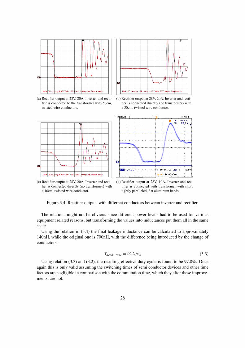
(a) Rectifier output at 28V, 20A. Inverter and recti-fier is connected to the transformer with 50cm,twisted wire conductors.
(b) Rectifier output at 28V, 20A. Inverter and recti-fier is connected directly (no transformer) witha 50cm, twisted wire conductor.
(c) Rectifier output at 28V, 20A. Inverter and recti-fier is connected directly (no transformer) witha 10cm, twisted wire conductor.
(d) Rectifier output at 28V, 10A. Inverter and rec-tifier is connected with transformer with shorttightly paralleled, flat aluminum bands.
Figure 3.4: Rectifier outputs with different conductors between inverter and rectifier.
The relations might not be obvious since different power levels had to be used for variousequipment related reasons, but transforming the values into inductances put them all in the samescale.
Using the relation in (3.4) the final leakage inductance can be calculated to approximately140nH, while the original one is 700nH, with the difference being introduced by the change ofconductors.
Tdead−time = L·2·Iin/Vin (3.3)
Using relation (3.3) and (3.2), the resulting effective duty cycle is found to be 97.8%. Onceagain this is only valid assuming the switching times of semi conductor devices and other timefactors are negligible in comparison with the commutation time, which they after these improve-ments, are not.
28

Another factor worth mentioning is that the new conductors also lead to a situation where theouter circuit is not affected much by the setup used, i.e. the circuit inductance is the same nomatter how the converter is twisted and pulled.
3.1.2 Synchronous rectication and eective duty cycle
When using the synchronous method of rectification the most important factor to set, in order tokeep up the effective duty cycle, is found in the gate driving circuit. The dead time due to circuitinductance is the same as before, but now there is also a risk of dead time induced by faulty gatedriving.
Without gate control the gate voltage and current will become much to high and simply shortcircuit and most likely break the MOSFETs. To keep this in check a gate driver needs to beimplemented. The scope of this driver is to make sure, enough charge is delivered to the gate asfast as the MOSFET switching time allows, but not faster.
Due to low gate current, one transistor might turn on, “long” before the other one turns off,resulting in a short circuit loop for a short time. This can be seen as the spikes in the draincurrent of Figure 3.5 and is often referred to as cross conduction. With a perfect gate driver andappropriate delay times the spikes seen in Figure 3.5 will not be visible at all.
Figure 3.5: Channel 1(Dark blue) drain current transistor 1, Channel 2 (Light blue) drain currenttransistor 2, Channel 3 (purple) Vgs transistor 1, Channel 4 (green) Vgs transistor 2
Achieving a perfectly synchronized switching without adding unwanted delay is not an easytask but was improved greatly by the gate drives described in later section 3.4.4.
29

3.2 Full bridge inverter losses
Due to certain initial constraints on easily available lab equipment, the initial power loss mea-surements and calculations are performed at a load level corresponding to 28V and 6A input.A fairly substantial degree of linearity is assumed at this point, which gives an adequate ap-proximation of reality. The only source of power loss considered in the inverter, is the onelocated in the MOSFET transistors. There is also resistive loss in the conduction paths on thecircuit board, but these are negligible in comparison. In this section, the MOSFETs originallyused in the inverter worked with, IRFP460LC, are compared with another choice of MOSFETs,IRFP044NPbF, that according to theory should work a lot better. The performance of these newtransistors is evaluated and put into context. The major difference between these two models ofMOSFET transistors is the on-state resistance. The old transistors have a resistance of 0,27Ω,while the new ones only have one of 21mΩ. Important to notice regarding the resistance of theMOSFETs, is that the old one were paralleled four and four while the new ones were used twoand two, resulting in 0,27Ω/4 and 21mΩ/2 respectively.
3.2.1 Original full bridge inverter - Old MOSFETs
The first thing to measure is the switching losses of the old transistors. This was as mentionedperformed at an input voltage of 28V and an input current of 6A, resulting in the losses presentedin Table 3.1.
Table 3.1: Calculated theoretical and measured actual switching losses of the original full bridge,at 28V and 6A input. Three different switching frequencies are tested: 55kHz,121kHz and 173kHz. Using a single secondary winding on the transformer (i.e. 2:4turns ratio)
Calculated Turn-on losses[W] Turn-off losses[W] Switching losses[W] Perc. of Pin
55 kHz 1.66 1.55 3.22 1.92 %121 kHz 3.66 3.42 7.07 4.21 %173 kHz 5.23 4.88 10.11 6.02 %
Measured55 kHz ≈0 1.56 1.56 0.93 %121 kHz ≈0 3.19 3.19 1.9 %173 kHz ≈0 4.41 4.41 2.63 %
When the actual measurements are performed it appears that the great commutation time, duethe inductance in the circuit, is greater than the turn-on time as can be seen in Figure 3.6.
30

Figure 3.6: Drain current (dark blue) and drain-source voltage (light blue) during a turn-on oc-casion for one of the MOSFETs in the inverter. The voltage reaches zero before thecurrent goes starts to increase (approximately)
The normal assumption when calculating turn-on losses is that the current goes up at the sametime as the voltage goes down, but as can be seen, the voltage goes down to VDS(on) long beforethe current reaches its high value. In effect, soft turn-on switching is applied. In this situation,a fairly high amount of current is to be conducted, resulting in a great dependence on the circuitinductance, which in turn is tricky to keep constant from setup to setup.
Another factor affecting the turn-off losses is the derivative of the drain current during theon-state. At 55kHz the current varies with 2A over the on-state period in the case without thecenter-tap (2:4 winding ratio). This in effect means that the current at the moment of turn-offis higher than the average current and lower than the average at turn-on. Fortunately this is anabsolute effect, and not a proportional one, so that at higher load currents this effect has a smallerimpact on the turn-off losses.
The other loss to consider is the on-state conduction losses. These were measured at the samevoltage and current levels as the switching losses and presented in Table 3.2.
31

Table 3.2: Calculated theoretical and measured actual conduction losses of the original fullbridge, at 28V and 6A. The measured values illustrates the point, but are due to mea-suring errors at the time of the measuring not possible to use as a verification.
Calculated Conduction loss [W] Percentage of input power55 kHz 4.46 2.65 %121 kHz 4.41 2.63 %173 kHz 4.36 2.60 %
Measured55 kHz 8.32 4.95 %121 kHz 8.23 4.90 %173 kHz 8.15 4.85 %
At the time these measurements were performed, measurement errors due to the very bigratio between high and low values in an oscilloscope were not yet known. This ratio leads tosaturation in a part of the amplifier within the oscilloscope when trying to zoom in, in a wayresulting in a big part of the waveform being outside the screen, (Calmels 2004). After themeasurement error was discovered, the voltage clamp described in Figure 3.7 was used to geta more accurate value of Vds,on. Fortunately the error is a proportional one and therefore bycomparing the values attained before the use of the voltage clamp and the ones after for the newMOSFETs, the measurement error of the on-state voltages of the old MOSFETs is found to beapproximately 40%. As a result, the conduction losses measured are a factor (1,4)2 larger thanthey ought to be.
32

3.2.2 Improved full bridge inverter - New MOSFETs
In Table 3.3 the theoretical switching losses for the new MOSFETs are shown. Assuming a casewith an unchanged external circuit inductance the turn-on losses will in reality still be very low(more or less zero) with the use of the new MOSFETs.
Table 3.3: Calculated and measured switching losses, using the new 55V MOSFETs, at 28Vand 6A. The transformer winding configuration used here is the case with a singlesecondary winding.
Calculated Turn-on losses[W] Turn-off losses[W] Switching losses[W] Perc. of Pin
55 kHz 1.48 0.96 2.44 1.45%121 kHz 3.25 2.11 5.37 3.20%173 kHz 4.65 3.02 7.67 4.57%
Measured55 kHz 0.0422 4.36 4.4022 2.62%121 kHz 0.155 4.18 4.335 2.58%173 kHz 0.22 3.6 3.82 2.27%
As the table shows, the values measured for the turn-off losses are not quite the same as theones calculated. This is mainly due to two facts. First, the magnetizing inductance of the trans-former affects the current derivative during the turn-on time, the same way as in section 3.2.1.Secondly it has to do with excessive overshoot of the voltage at the moment of turn-off. This isdue to that the new transistors switch faster and thus allow a higher δ i/δ t within the transistor. Ifdisregarding all the overshoots and odd ringing, the switching times of the new transistors canstill be found to be approximately 50ns at both turn-on and turn-off. As this is roughly the sameas the old ones, the switching losses ought to be roughly the same as for the old ones as well.
At a later point the circuit was stable enough and the lab equipment required was available tomeasure the switching losses at a higher power level.
To find the overall loss in voltage as well as the conduction loss of the full bridge, the on-statevoltage drop needed to be measured, which was done according to Figure 3.7.
33

Figure 3.7: Connection used in order to measure the on-state voltage of SW4 with an acceptablysmall error.
In order to get realistic and accurate results, a voltage clamp is needed to keep the ratiobetween the on-state and the off-state voltage down. A simple voltage clamp, using a 12V zenerdiode, a 1N4148 diode and a 3.9kΩ was used. The exact value of the resistance is not important,the only thing considered is that the current in the parallel path is kept negligibly low while theresistance is still kept well below the value of the non-conducting diodes (i.e. when the diodesare not conducting, more or less the whole voltage should be over the diodes). The resultingconduction losses measured with this setup, as well as the theoretical one calculated from thedata sheet, are presented in Table 3.4.
Table 3.4: Calculated and measured conduction losses, using proposed choice of MOSFETs, at28V and 6A.
Calculated Cond. loss Perc. of Pin
55 kHz 0.72 W 0.43 %121 kHz 0.71 W 0.42 %173 kHz 0.7 W 0.42 %
Measured55 kHz ≈ 0.96W 0.57%
121 kHz ≈ 0.96W 0.57%173 kHz ≈ 0.96W 0.57%
34

The low power parameters found for the new mosfets are not quite as good as the data sheetsclaim, however despite the difficulties in getting stable and nice waveforms, they still show anover all large difference from the old ones, as seen in Figure 3.8. In the graph of Figure 3.8, onlythe conduction losses are shown, however these are very important as they, unlike the linearlyincreasing switching losses, increases with the square of the current.
Figure 3.8: Conduction losses of the old and the new MOSFETs at different input powers.
Finally, with a stable rectifier, the losses of the inverter were measured again at a higher powerlevel. At 55kHz, 27.9V input voltage and 16.1A input current, the final values presented in Table3.5were acquired. As can be seen, at this higher power level the switching losses have leveledout to be approximately 1% just as for the old MOSFETs at the lower power level.
Table 3.5: Summarized final losses of the inverter, at an input power of 450W.Loss relative to input power (450W)
Switching loss [Percent of input power] 1.15 %Conduction loss [Percent of input power] 2.18 %
Vds,on [V] 0.16 V
35

3.3 RotatingTransformer eects
For the cases of synchronous rectification, without the center-tap, the total leakage inductanceof the system before the output filter is found with the relation:
Lleakage =Vin ·Tdead−time
2 · Iin(3.4)
Here it is found to be approximately 140nH while in the case for the center-tap the total leakageinductance is approximately 66nH. This is found by looking at the time of zero voltage in Figure3.9b and Figure 3.9a, in which the dead-time of the two different configurations, measured rightbefore the output filter are shown.
(a) Single secondary winding. Output of the rectifier at oneswitching occasion at 28V and 10A input.
(b) Center-tap configuration. Output of the rectifier atone switching occasion at 28V and 20A input.
Figure 3.9: Dead-times found with and without the use of center-tap. The plots depict a switch-ing occasion of the voltage over the rectifier output.
36

Looking back at the theoretical values of the leakage inductances found in Table 2.1 for thetransformer, the leakage inductance for the case with the center-tap appears to be about 20nHlarger than the theory. Considering that the theoretical values did not at all consider the differ-ences between the cases, namely that with a center-tap configuration there will always be a morecomplicated connection (inductance wise), this is not very odd. In any case there is about twiceas much leakage inductance with the single secondary winding case compared to the center-tapcase, resulting in a longer dead time for each switching occasion.
As for the effect of the magnetizing inductance, a no load test reveals a magnetizing current of1.1A and 0.1A for the center-tap configuration and the single secondary winding configurationrespectively. At an input voltage of 27.9V this translates to a core loss of 30.7W with thecenter-tap and 2.8W with the single secondary winding. All the resulting measured transformerparameters are shown summarized in Table 3.6.
Table 3.6: Transformer parameters. One thing important to notice in this table is that the leakageinductance mentioned is not just the internal leakage inductance of the transformer,but the whole part of the circuit leakage inductance affected by the choice of trans-former configuration.
Center-tap Single secondary winding1:2:2 2:4
Magnetizing current 1.1A 0.1ALeakage inductance ≈ 31.25nH +20nH = 51.25nH 125nH
Total circuit leakage inductance 66nH 140nHCore loss 30.7W 2.8W
37

3.4 Rectier voltage - and power loss
In chapter 2, the different rectifiers evaluated in this thesis are presented:
• Full wave diode rectifier - Single secondary transformer winding
• Full wave diode rectifier - Center-tap on secondary transformer winding
• Self-driven synchronous rectifier - Center-tap on secondary transformer winding
• Self-driven synchronous rectifier - Single secondary transformer winding
In this section, these are investigated with regards to voltage loss, power loss, effective dutycycle as well as complexity of components and control of components. This is performed inorder to provide arguments for reasonable tradeoffs between different solutions. From this partand on, a switching frequency of 55kHz is used, since this currently is the only option that allowsfor decent duty cycles.
3.4.1 Measurements on the full wave diode rectier - Single secondarywinding
The single phase diode bridge was never meant to be the rectifier used in the end due to therelatively large voltage drop across the four diodes compared with transistors. However, it wasa solution that was good enough at the starting point. Its main purpose was simply to rectify andprovide the load a DC-voltage and complete the system to see if everything worked as intended.It also provided a first evaluation of the aspects of the rectifier needed to be worked with. Forsimplicity, the preferred diode package was TO-247 since it could easily be mounted into thealready existing empty slots on the full bridge chassis that were used for cooling. This packagecan provide a low thermal resistance and with a cooling fan temperatures could be kept withinnormal operation limits.
The blocking voltage of the rectifier needed to be larger than the output voltage of the trans-former but also with respect to the possible voltage ringing, that will occur due to the interactionof the circuits leakage inductance and the parasitic junction capacitance of the diodes.
The ultra fast switching diode, STTH6002CW, specified as suitable for switch mode powersupplies, SMPS, and high frequency DC/DC-converters was chosen. It has a maximum RMSforward current of 50 A and a blocking voltage of 200V.
Measurements were made at Vin = 28V, an input current of 15 A and a switching frequencyof 55kHz. The obtained waveforms of the diode output voltage (pink) and the output voltageafter the output filter (green) are shown in Figure 3.10. It can be seen that the largest spike of thevoltage ringing is slightly more than 140V. This unwanted ripple causes excessive power loss ofthe diode bridge and put high stress on the diodes.
38

Figure 3.10: Picture of a switching occasion at the rectifier output. The purple channel is thepre-filter voltage and the green one is the resulting average output voltage.
The voltage drop across each diode was measured to 0.8V which leads to a total drop of 1.6Vacross the whole bridge. Due to the transformer design with a ratio of 1:2, this large drop is notacceptable if the aim is an output voltage twice that of the input.
3.4.2 Measurements on the full wave diode rectier - Center-tap onsecondary winding
For this rectifier setup, two diodes of the same type that was used in the previous rectifier werealso used here. During all measurements, the wires had been replaced with flat aluminum bandsconnected between the full bridge converter, transformer and the rectifier. The wires were madeas short as possible in order to minimize their inductance and the conductors were bundledas tightly as possible. The obtained values of the currents below were taken from the internalampere meter of the power supply at 55kHz switching frequency and Vin and Vout were measuredusing the oscilloscope. With the load adjusted to give the input characteristic below:
Uin = 28V
Iin = 18A
Pin = 28V ·18A = 504W
the output voltage was measured to 52.43V.To find the efficiency, the output power needs to be known. As there at this moment were no
accurate current probes easily available, the output power was instead found by measuring theDC-resistance of the load with a simple FLUKE multimeter. The load resistance at this powerlevel was found to be approximately 6.75Ω, resulting in an output power of:
39

Pout =U2
out
Rload=
52.432
6.75= 407.25W
This results in a total efficiency of:
η =Pout
Pin=
407.25504
= 80.8% (3.5)
While there were losses all over the converter, extreme heat dissipation made it obvious with-out measurements that a great part of it came from the rectifier diodes. A lot of further workcould be done with the voltage ringing and efficiency here, but a decision was made to startinvestigating synchronous rectification instead.
3.4.3 Measurements on the self-driven synchronous rectier - center-tapon secondary transformer winding
The main aspect to look at when choosing a rectifier transistor is its on-state resistance, Rds,on,since it will determine the size of the voltage drop across each unit when conducting. The tran-sistors chosen for this rectifier are IRFP4227PbF which have an Rds,on of 21mΩ and a switchingspeed of approximately 30ns. They are capable of blocking voltages up to 200V and can con-duct a maximum continuous drain current of 65A. The switching speed is not that important aslong as it is higher than that of the primary side inverter switches, since these directly pull thesecondary side’s gate voltages.
In the center tapped synchronous rectifier, the voltage across each secondary winding isVrecti f ier. If the setup in Figure 2.7 is used, the transistor gates must be able to withstand twicethe output voltage of the transformer. In this case, at full voltage, there would be around 114Vand therefore this setup is initially only tested at input voltages of up to 7V, resulting in a 28Vgate-source voltage. To be able to pull the voltage up, a resistive/capacitive voltage divider asshown in Figure 3.11 was connected between the gate and source on each transistor.
Figure 3.11: Voltage divider used in order to not expose the MOSFET gates to over voltages.The zener-diode clamps the voltage over the gate-source nodes to its maximumreverse voltage, in this case 12V.
40

At a drain current of 4A the resulting on-state voltage drop was measured to be approximately80mV, verifying that this way of using the transistors instead of diodes, indeed works. Whenthe function of the transistors was verified, it was concluded that the high core loss of the trans-former (1.1A*27.9V) with the center-tap configuration was not worth the gain of using one lesstransistor and therefore the single secondary winding solution was carried on with.
3.4.4 Measurements on the self-driven synchronous rectier - singlesecondary transformer winding
To achieve synchronous switching, without endangering the transistors, the transistor gates weredriven in pairs using two pulse transformers, each having two secondary windings. The pulsetransformers’ primary windings were connected across one turn of the rotating transformer’ssecondary windings, hence a gate voltage of 56/4= 14V was attained, see Figure 3.12.
To provide the MOSFET gates with a controlled amount of current, a gate resistor, Rg, wasconnected in series with the input of the pulse transformer. According to the data sheet, at Vgs =10V, a gate resistor of 2,5Ω was used to attain the switching times of approximately 30ns, asso-ciated with this transistor. However, due to the gate pulse voltage of 14V, a 40% larger resistorwould in theory be necessary. The switching speed of the primary side inverter transistors islimited to approximately 50ns and since the pulse transformer is connected directly to the sec-ondary side of the transformer, so are the rectifier transistors. Therefore, there is no need to usea smaller resistor than what would lead to a switching speed of 50ns. A gate resistor of 7,8Ohmresistor was chosen as an appropriate value.
The measured drain-source voltage of the transistors in the rectifier contained large amount ofripple, resulting in the need of a snubber in order to prevent damaging of the components. Thesnubbing procedure is described in section 3.5.
41

Figure 3.12: Connection used to acquire a voltage clamp for the off-state voltage level. Whenthe drain-source voltage goes high, the probe sees only the forward voltage of the1N4148 diode. T2 and T3 are the pulse transformers used to deliver gate pulsesfrom the secondary winding of the transformer to the rectifier MOSFETs.
In order to get a more accurate measurement of Vds,on a voltage clamp similar to the one usedon the inverter, was applied, according to Figure 3.12.
After snubbing the rectifier MOSFETs according to section 3.5, the final resulting voltagedrops and power losses of the rectifier was measured, using the measuring procedures presentedearlier (voltage clamps between the drain and source of transistors). These values are shown inTable 3.7.
Table 3.7: Rectifier losses, measured at 55kHz, 27,9V input voltage and 16,1A input current.Percentage of input power
Switching loss [Percent of input power] 0.55 %Conduction loss [Percent of input power] 0.57 %
Loss in rectifier snubbers [Percent of input power] 0.21 %Vds,on [V] 0.155 V
42

3.5 Snubber design
In section 2.4 the basic idea behind the snubber design is described. In reality measuring boththe effective capacitance and the total leakage inductance of the circuit is often hard. In (Ridley2005) a simpler approach is described in which the characteristic impedance is approximatedwith the use of the undampened ringing frequency and just one of these two parameters. At450W the ringing frequency is directly measured over the drain to source voltage of the rectifiertransistors to be 25MHz with the use of an oscilloscope. The leakage inductance was presentedin Table 3.6 to be 140nH. With these values the snubber resistor can be calculated as:
Rs = Z0 = 2 ·π · fringing ·L = 2 ·π ·16e6 ·140e−9 = 14Ω (3.6)
when the snubber resistor value is known the next thing to calculate is the snubber capacitor.
Cs =1
Rs · fringing= 4nF (3.7)
However, using this snubber capacitor led to much more dampening than needed and greatlyaffected the system, making it much too slow and greatly reducing the efficiency. A compromisethat worked well was to instead use a 100Ω resistor and with the same reasoning a resulting0.7nF capacitance.
Rs = 100Ω
Cs = 0.7nF
Important to note here is that this is not the ideal snubber, it is simply as mentioned, an acceptablecompromise.
3.6 Output lter design
In order to aquire the desired output voltage a simple output filter was designed. A simpleapproach to this design procedure can be summarized with:
Uinductor = Linductor ·∆i∆t⇒ Linductor =Uinductor ·
∆t∆i
(3.8)
With some exaggeration the worst case scenario dead time can be approximated to 10%. Witha desired average output voltage of 56V that means we have a peak voltage of 56/0.9≈ 62V and aconduction time of approximately 9µs for each half period. The voltage Uinductor in (3.8) refersto the voltage over the inductor, i.e. the difference between the output voltage of the rectifierand the average voltage. Looking at, for instance, the conducting part of the half periods, theinteresting area, Uinductor ·∆t , becomes the area covered by the red grid in Figure 3.13.
43

Figure 3.13: Schematic picture illustrating the output of the rectifier pre-filter, contra the averagevoltage output obtained after the filter.
Approximating the allowed current ripple through the inductor to 1A, for simplicity, leads via(3.8) to an inductance:
L f ilter =(62−56)V · 1
110kHz·0.9
1A= 49µH (3.9)
Looking at the current-waveform through the inductor, Figure 3.13, the charge needed tobe absorbed and released by the output capacitor every half period can be found using simplerelations. The charge consists of the difference between the actual current through the inductorand the output average current, which would ideally be fully DC.
QC =∆i/2 · Tsw/(2·2)
2=
1A/2 · 18.2µs/4
2= 1.14µAs (3.10)
Accepting a voltage ripple of 0.5V, the capacitance value can be found with the relation:
C f ilter =QC
Vripple=
1.14µAs0.25V
= 4.56µF (3.11)
The -3dB cut-off frequency of this LC-filter becomes
fcut−o f f =1
(2π)√
L f ilter ·C f ilter≈ 10.7kHz
which is well below the 100kHz output of the rectifier considered.
44

After the desired values of the inductor and capacitor of the filter has been found, the designof the inductor begins.
Going one step further from the relation in (3.8) another known relation can be applied:
Uinductor = Linductor ·∆i∆t
=∆B∆t·AFe ·Ninductor (3.12)
where B is the magnetic flux density and AFe is the cross section area of the core
Linductor =B ·AFe ·Ninductor
i(3.13)
At the time this inductor was designed the peak of the current worked with was about 5A andthe inductor was thus designed for that area in order to get started with the rectifier. The exactcore used is unknown, as it is an old component being reused, however it is a ferrite E-core. Tostay well below saturation levels of the ferrite core, a maximum magnetic flux density of 0.2T isassumed.
Ninductor =Linductor · i
B ·AFe=
49µH ·5A0.2T ·340µm2 = 3.6 turns (3.14)
Since later on a greater current is desired, the number of turns are slightly exaggerated intothe number of turns there happen to be room for, namely seven. An additional reason for thisaction is that filling the available area with extra turns makes acquiring a tight and well coupledwinding easier. Finally to make sure the magnetic flux density within the core is kept downbelow saturation levels, an air gap is introduced.
Using the relation of (3.13) once again in combination with Ampere’s law gives:
Ni = B(
lcore
µcore+
lgµ0
)≈ B
lgµ0
(3.15)
B≈ N2 iµ0
lg(3.16)
lg ≈AFeµ0
Linductor/N2=
340µm2 ·4π10−7
49µH/72≈ 0.4mm (3.17)
45

4 Conclusion
4.1 Results and discussion
4.1.1 Inverter
Measurements and simulations of the losses and performance of the simple full bridge inverterproposed in Chapter 2 verify that this topology is indeed adequate for the voltage - and power-interval considered. With the use of the two parallel IRFP044NPbF MOSFET transistors , theefficiency reaches 94.4% at 450W. The majority of the losses originates from the inverter anda possible source of concern is the conduction losses, which would increase exponentially incase of an increased power level, as seen in Figure 3.8. This could however easily be improvedfurther with the use of either better transistors with a lower RDSon or simply a greater numberof parallel connected transistors. In Table 4.1 the different sources of loss in the converter areshown.
Table 4.1: Losses of the resulting converter at an input power of 450W.Source of power loss Losses [Percent of 450W input power]Inverter conduction 1.15%Inverter switching 2.18%
Transformer magnetization and resistive ≈0.97%Rectifier conduction 0.55%Rectifier switching 0.57%Rectifier snubbers 0.21%
Complete DC/DC-converter 5.63%
As can be deduced from the table, the inverter conduction is the only major issue at thismoment. If the input power was to be doubled, closing in on the 1000W load that was originallyconsidered, the inverter conduction would be the single greatest source of power loss of theconverter and would be in need of reduction. The switching losses are what they are and willnot be affected by load level, since the switching loss relation is linear with current.
46

4.1.2 Transformer
For the sake of the rest of the converter the use of a center-tap configuration of the transformerwindings would be ideal, however with the specific transformer worked with in this thesis, it issimply not viable, due to the low number of turns and thus low magnetization inductance. At500W the different power losses of center-tap and single secondary winding configurations areapproximately 30.7W and 2.8W respectively. In fact, the low magnetic inductance has a doublenegative impact on the converter since the inverter turn-off losses is the single greatest sourceof power loss in the system and this increases further with a lower magnetizing inductance andthus higher drain current at the moment of turn-off, although this is mostly an issue at lowpower levels. Apart from not being able to use the center-tap, the drawback of using the singlesecondary winding configuration is that it results in a higher leakage inductance, as well as thedesired higher magnetic inductance. The resulting leakage inductance of the transformer comesto 125nH out of a total of 140nH for the entire converter.
4.1.3 Center-tap
To achieve a center-tap connection and a 1:2 ratio with the transformer with only 4 windingturns available on primary and secondary, a winding ratio of 1:2:2 must be used. Apart fromperforming its task of supplying two windings on the secondary side this also greatly affectsthe magnetizing inductance of the transformer. As mentioned in Section 2.2.2, the inductanceis proportional to N2
1 . With a single secondary winding, a turns ratio of 2:4 can be used for thetransformer. Due to this, the magnetizing inductance is reduced with a factor 22 = 4. The effectof this is that the magnetizing current needed to magnetize, i.e. charge up the transformer isgreatly increased. The resulting magnetizing current for the center-tap connection is approxi-mately 1,1A. With an input voltage of 28V the power loss of the magnetizing comes up to anunacceptable level of 30,8W.
47

4.1.4 Rectier
The most beneficial rectifier topology was found to be the four transistor self-driven synchronousrectifier shown in Figure 2.8, with the gate signals taken from the transformer secondary viasmall pulse transformers. With the switches consisting of two IRFP4227PBF MOSFETs inparallel, the rectifier losses could be kept at about 1% at an input power of 450W. With thesetransistors basically working as enhancement diodes, a non-negligible voltage ringing is intro-duced that needs to be snubbed, in order to protect the transistors as well as reduce losses. Thesnubbers used are designed to dampen no more than needed; keep the turn-off voltage peaksbelow 130V and introduces an extra loss of approximately 1W total in the rectifier. The max-imum duty cycle achievable at 450W is 97% where 1% of the loss of duty cycle comes fromthe switching times of the rectifier transistors (and indirectly the switching times of the invertertransistors). At 28V and 15A input, this in combination with the various voltage drops withinthe circuit leads to an output voltage of 52.9V.
In Figure 4.1, a rough approximation of the input - and output- voltage relation is shown.The plot is derived from known voltage drops and causes of duty-cycle loss with a slight ap-proximation regarding the input current, in order to find the duty-cycle for each condition. Thisapproximation is that the input current is approximately 95% of the output current multipliedwith two (from the transformer).
Figure 4.1: Graph of relation between input voltage and output voltage of the full converter. Thepreviously determined acceptable voltage input (24-30 V) - and output (48-60 V)-levels are illustrated by the black dashed lines.
48

The way to interpret Figure 4.1 is that the point at which the plotted lines cross the verticaldashed lines sets the limit for which input voltages are acceptable in order to achieve an outputvoltage within the desired interval. From this plot, some application limitations can be found.The most interesting one is the fact that the interval of acceptable input voltage variations inorder to get an output voltage within the accepted interval is moved to the right (higher values)with increased power level. This effectively sets a higher demand on the input voltage withincreased load.
4.1.5 Inuence on the leakage inductance caused by the switchingfrequency
Since the absolute dead time is unrelated to the frequency used for switching, the effectiveduty cycle would be less affected by this dead time, with a longer switching period. A lowerswitching frequency is therefore strongly preferred if the dead time is of considerable size. Thelowest switching frequency possible with the inverter control used is 55kHz, which is thereforechosen.
The possible advantage of having a high switching frequency is the ease of canceling the out-put current ripple. Smaller filter can be used, hence the size and cost can be reduced. However,the loss of duty cycle due to a higher switching frequency is of far more concern in this designin order to achieve the desired output voltage.
49

4.2 Future work
• A factor of great importance for this converter is the air gap of the transformer. Due tocertain imperfections in physical design of the current transformer the air gap can notbe reduced below approximately 3mm without compromising the transformers ability torotate without friction. If the iron parts of the transformer was further processed andgreatly smoothed the air gap could theoretically be greatly reduced. If for instance theair gap could be reduced with a factor 4, the magnetizing inductance of the case with thecenter-tap would be approximately that of the current case without the center-tap. Thiscould potentially allow for the use of the center-tap configuration, which would greatlyreduce the leakage inductance and thus the dead-time associated with it as well as slightlyreduce the power losses and voltage drops of the rectifier MOSFETs.
– In the transformer today there is also a lot of unused space, which with a redesigncould allow for more windings => more primary turns => more magnetizing induc-tance.
• Another partly mentioned point of interest could be the turns ratio of the transformer.The limitation is set so that the output voltage of the rectifier, pre-filter (excluding spikes)must not exceed 60V. With a maximum input voltage of around 28V this would allow fora turns ratio of up to 1:(2,14). With this ratio, voltages even slightly above 56V wouldbe possible, which in turn would allow for an additional control feature. Since the deadtime is a function of the input current, the phase shift control could be used in order toincreased the dead time when the input current and thus the dead time decreases.
• Worth mentioning is also the fact that the inverter used in this thesis is originally designedto have phase shifting capability to allow resonant soft-switching. If a brand new inverterwas designed, where this capability was not introduced, as would be the case for thecurrent application, the inverter could be snubbed in order to lag the turn-off voltages andgreatly reduce the turn-off losses.
• If implementing this converter in reality an active snubber that could handle dampening ofthe voltage without decreasing the speed characteristics of the converter too much wouldbe a great improvement. This could possibly increase the efficiency by another percent,putting the switching losses of the inverter closer to that of the theoretical response, whereovershoot was not considered.
• In the next version of the transformer; Optimize connections for the transformer windings.Currently the winding configuration is controlled by physical windings sticking out fromthe transformer, leading to extra stray inductance and degradation of the form factorsaffecting the leakage - and magnetic - inductance.
50

5 References
1. Andreycak Bill. (1997) Phase shifted, zero voltage transition design considerations andthe UC3875 PWM controller. Unitrode Application note.
2. Calmels Alain. (2004) VDS(on), VCE(sat) Measurement in a High Voltage, High Fre-quency System. Advanced Power Technology Europe. Application note.
3. Hagerman Jim. (1995) Calculating Optimum Snubbers. Hagerman Technology
4. Papastergiou Konstantinons D. and Macpherson D. Ewen. (2007) An Airborn RadarPower Supply With Contactless Transfer of Energy - Part 1: Rotating Transformer. IEEETransactions on Industrial Electronics. Vol. 54, NO.5.
5. Papastergiou Konstantinons D. and Macpherson D. Ewen. (2007) An Airborn RadarPower Supply With Contactless Transfer of Energy - Part 2: Converter Design. IEEETransactions on Industrial Electronics. Vol. 54, NO.5.
6. Ridley Ray. (2005) Flyback Converter Snubber Design. Designer Series XII. SwitchingPower Magazine.
7. Schade Nicholas J. Core Losses in Composite Inductors. Vishay Intertechnology Inc.
8. Undeland, Mohan and Robbins. (2003) Power Electronics Converters, Applications, andDesign. Third Edition John Wiley & Sons, INC.
51


