Design and Evaluation of A Low-Voltage, Process- Variation-Tolerant SRAM Cache in 90nm CMOS Technology Master’s thesis Performed in Electronic Devices By Ali Fazli Yeknami Reg nr: LiTH-ISY-EX--08/4172--SE March 2008
Transcript
Design and Evaluation of A Low-Voltage, Process-Variation-Tolerant SRAM Cache in 90nm CMOS
Technology
Master’s thesis Performed in Electronic Devices
By Ali Fazli Yeknami
Reg nr: LiTH-ISY-EX--08/4172--SE
March 2008
Design and Evaluation of A Low-Voltage, Process-Variation-Tolerant SRAM Cache in 90nm CMOS
Technology
Master’s thesis Performed in Electronic Devices, Dept. of Electrical Engineering
at Linköpings Universitet
By Ali Fazli Yeknami
Reg nr: LiTH-ISY-EX--08/4172--SE
Supervisor: Professor Atila alvandpour Linköpings Universitet Examiner: Professor Atila alvandpour Linköpings Universitet Linköping, March 2008
Presentation Date 2008-04-04 Publishing Date (Electronic version) 2008-06-17
Department and Division Department of Electrical Engineering Electronic Devices
URL, Electronic Version http://www.ep.liu.se
Publication Title Design and Evaluation of A Low-Voltage, Process-Variation-Tolerant SRAM Cache in 90nm CMOS Technology Author(s) Ali FazliYeknami
Abstract
This thesis presents a novel six-transistor SRAM intended for advanced microprocessor cache application. The objectives are to reduce power consumption through scaling the supply voltage and to design a SRAM that is fully process-variation-tolerant, utilizing separate read and write access ports as well as exploiting asymmetry. Traditional six-transistor SRAM is designed and its strengths and weaknesses are discussed in detail. Afterwards, a new SRAM technology developed in the division of Electronic Devices, Linköping University is proposed and its capabilities and drawbacks are illustrated deeply. Subsequently, the impact of mismatch and process-variation on both standard 6T and proposed asymmetric 6T SRAM cells is investigated. Eventually, the cells are compared regarding the voltage scalability, stability, and tolerability to variations in process parameters. It is shown that the new cell functions in 430mV while maintaining acceptable SNM margin in all process corners. It is also demonstrated that the proposed SRAM is fully process-variation-tolerant. Additionally, a dual-V t asymmetric 6T cell is introduced having wide SNM margin comparable with that of conventional 6T cell such that it is capable of functioning in 580mV.
Keywords SRAM, Traditional 6T, Asymmetric 6T, memory, SNM, cell
Language
English Other (specify below) Number of Pages 106
Type of Publication Licentiate thesis
Degree thesis Thesis C-level Thesis D-level Report Other (specify below)
ISBN (Licentiate thesis) ISRN:
Title of series (Licentiate thesis) Series number/ISSN (Licentiate thesis)
Abstract This thesis presents a novel six-transistor SRAM intended for advanced microprocessor cache application. The objectives are to reduce power consumption through scaling the supply voltage and to design a SRAM that is fully process-variation-tolerant, utilizing separate read and write access ports as well as exploiting asymmetry. Traditional six-transistor SRAM is designed and its strengths and weaknesses are discussed in detail. Afterwards, a new SRAM technology developed in the division of Electronic Devices, Linköping University is proposed and its capabilities and drawbacks are illustrated deeply. Subsequently, the impact of mismatch and process variation on both standard 6T and proposed asymmetric 6T SRAM cells is investigated. Eventually, the cells are compared regarding the voltage scalability, stability, and tolerability to variations in process parameters. It is shown that the new cell functions in 430mV while maintaining acceptable SNM margin in all process corners. It is also demonstrated that the proposed SRAM is fully process-variation-tolerant. Additionally, a dual-V t asymmetric 6T cell is introduced having wide SNM margin comparable with that of conventional 6T cell such that it is capable of functioning in 580mV. Keywords: SRAM, traditional 6T, asymmetric 6T, memory, SNM, cell
v
Acknowledgement
In the process of writing this thesis, I have had insightful discussions, received helps, and support from many people and I would like to take the opportunity to thank them here.
First of all, I would like to thank my supervisor, Professor Atila Alvandpour, who has always been willing for open discussions. I have really taken the advantage of his open door policy and his knowledge of corporate valuation and I am grateful for all the resourceful ideas and comments that helped me to forward.
Second, I would like to especially thank my assistant supervisor, Martin Hansson, who has always been available for questions and open discussions. This thesis would not have been possible without his support in Cadence and MATLAB as well as his insightful ideas. Here, I give my highest appreciation to him.
I would also like to thank my family for their encouragements, particularly, Hamze, who supported me a lot to complete this work.
Finally, I would like to thank PhD students of VLSI group for their support. Henrik Fredriksson, Timmy Sundstrsom, and Behzad Mesgarzadeh. Thank you all.
6 Future Work 79 Chip Fabrication and Measurement . . . . . . . . . . . . . . . . . . . . . . . 79 Design of Ultra Low-voltage Asymmetric 6T SRAM Cell . . . . . . 79 Study of Leakage Power in Asymmetric 6T SRAM Cell . . . . . . 80 Study of Static Noise Margin in Sub-V t Asymmetric 6T SRAM Cell
. . . . . . . . . . . . . . . . . . . . . . . . . . . . . . . . . . . . . . . . . . . . . . . . . 80 References 82 Appendix 85 A Derivation of SNM for Conventional 6T Cell . . . . . . . . . . . . . . . . 85 B Additional Simulation Results for 6T 88 B.1 6T Cell, process Corner Analysis . . . . . . . . . . . . . . . . . . . . . . . . 88 B.2 6T Memory Array, Read and Write Operations . . . . . . . . . . . . . . 90 C Additional Simulation Results for AS-6T 91 C.1 AS-6T Cell, Process Corner Analysis . . . . . . . . . . . . . . . . . . . . 91 D Cadence Simulation File for Monte Carlo Analysis 93 D1 Monte Carlo simulation Set-up for 6T Cell . . . . . . . . . . . . . . . . . . 93 D2 Monte Carlo simulation Set-up for AS-6T Cell . . . . . . . . . . . . . . . 95 E MATLAB Script 97 E.1 MATLAB Script for Monte Carlo Analysis for 6T Cell . . . . . . . . 97 E.2 MATLAB Script for Monte Carlo Analysis for AS-6T Cell . . . . 101
“The world's a scale where men are weighed – The worse they are the more they boast; But that's the way that scales are made –
The emptier pan's the uppermost. ” Ferdowsi
Chapter 1 Introduction 1.1 Overview
A major part of any electronic system is the memory subsystem. State-of-
the-art microprocessor designs devote a large fraction of the chip area to the memory structures. For instance, 30% of Alpha 21264 and 60% of StrongARM are devoted to cache and memory structures [1].
High-performance large-capacity Static Random Access Memories (SRAMs) are a crucial component in the memory hierarchy of modern computing systems. SRAM design requires a balancing act between delay, area, and power consumption. The circuit styles for the decoders and the sense amps, transistor sizing of the circuits, interconnect sizing and partitioning of the SRAM array can all be used as a tradeoff for these parameters.
In recent years, power consumption has become a critical design concern for many VLSI systems. In the meanwhile, memory accesses consume a substantial portion of the total power budget for many applications. The system-on-chip (SoC) employs a large number of SRAM as on-chip memory. Thus, reducing the power dissipation in SRAMs can significantly improve the system power-efficiency, performance, reliability, and overall costs.
An effective solution to the Power reduction is operation in sub-threshold regime. The sub-threshold regime is a critical biasing space as it enables minimum energy operation for logic circuits [2]. However, practical
1
2 Introduction
systems rely heavily on SRAMs which conventionally limit the minimum V DD to above Vt. SRAMs often dominate the total die area and power, and minimizing their energy requires scaling V DD as low as possible [3]. During recent years, SRAMs have experienced a very rapid development of low-power low-voltage memory design due to an increased demand for laptops, portable communication devices and IC memory cards. While CMOS technology has served semiconductor industry marvelously, it faces some major obstacles at sub-90nm process nodes due to the intrinsic physical limitations of the devices. One of the major barriers that the CMOS devices face at nanometer scale is increasing process parameter variations. Due to limitations of the fabrication process (e.g. sub-wavelength lithography and etching) and variations in the number of dopants in the channel of short channel devices, device parameters such as length (L), width (W), oxide thickness (tox), threshold voltage (Vt), etc. suffer large variations. Variations in the device parameters translate into variations in circuit parameters like delay and leakage power, leading to loss in parametric yield. To deal with increasing parameter variations, it is important to accurately model the impact of device parameter variations at circuit level and develop process-tolerant design techniques for both logic and memory. This study will examine the impact of process parameter variations on SRAM.
1.2 Objective
The main purpose of this thesis is to propose a new approach to the design of a low-voltage SRAM memory with particular focus on process parameter variations. In primary chapters the traditional 6T SRAM cell is studied and an architecture based on that will be introduced. Subsequently, a completely novel approach, called Asymmetric 6T SRAM cell (AS-6T), will be proposed and an architecture based on that will be presented. Voltage Scalability and functional stability of both traditional 6T and Asymmetric 6T cells is examined. Moreover, mismatch and process variation on single cell of both cells will be studied and afterward the investigation results will be compared. Eventually the designed AS6T cache is evaluated.
Therefore the main goals of this research can be highlighted as:
1.3 Thesis Organization 3
1. Develop novel approach of low-voltage asymmetric 6T (AS-6T) SRAM cell 2. Determine the capabilities of AS-6T cell with respect to voltage-scalabili- ty, process-variation-tolerance, and stability. 3. Determine the capabilities of standard 6T cell with respect to voltage- scalability, process-variation-tolerance, and stability. 4. Compare the asymmetric 6T cell with the conventional 6T cell with respect to voltage-scalability, process-variation-tolerance, and stability. 5. Evaluate a fabricated cache in 90nm technology that is based on proposed asymmetric 6T cell and demonstrate that the asymmetric 6T cell is functional in lower voltage than standard 6T SRAM cell. It is also shown that the asymmetric 6T cell is more process-variation-tolerant than conventional 6T cell.
1.3 Thesis Organization
Chapter 1- Introduction: presents a brief introduction and overview of general requirements and challenges in the design of low-voltage and process-variation-tolerant SRAM cache. It also includes some of the terms and acronyms used in the rest of this thesis.
Chapter 2– Traditional 6T SRAM: illustrates the basic structure of the traditional 6T cell, read and write functions, and periphery circuits. Subsequently, both read and write cell stability is investigated. dc and transient analyses of the cell are presented. In addition, a cache architecture utilizing 6T cell is introduced. Its read and write operations and cell stability in different supply voltages are studied. Eventually in the end of the chapter, some of the most recent research works in the design of ultra low-voltage SRAM cell are discussed. Chapter 3– Proposed SRAM Technology: Asymmetric 6T Cell: demonstrates a fully novel approach in the design of SRAM cell that is called Asymmetric 6T SRAM cell. The basic structure of the cell, read and
4 Introduction
write functions, and the cell stability is described. dc and transient analyses are presented. In addition, a cache architecture utilizing AS-6T cell is introduced. A technique improving the stability of AS-6T cell is described. Eventually, the cell read and write operations as well as the cell stability in different supply voltages are illustrated. Chapter 4– Study of Mismatch and Process-Variation: In-die variations and die-to-die variations for both standard 6T cell and proposed asymmetric 6T cell are investigated. Chapter 5– Traditional 6T and Invented Asymmetric 6T: Overall Comparison: The major advantages and disadvantages of each cell are illustrated in this chapter. Also the scalability of supply voltage for both cells as a comparable quantity is introduced and functionality of each cell in different. Both cells are compared with respect to mismatch, process-parameter-variation, and temperature variation.
Chapter 6– Future Work: Presents some recommendations and guidelines for future related studies and propose some topics for interested student. 1.4 List of Acronyms
Terms and acronyms mostly used in this thesis are listed as follows: 6T six-transistor AS-6T Asymmetric Six-transistor SRAM cell BBG Body-Bias Generator BL bitline BL bitline-bar CMOS Complementary Metal-Oxide-Semiconductor CS Column Selector EQ Equalizer FF N-fast P-fast FS Fast NMOS Slow PMOS GND Ground IC Integrated Circuits
1.4 List of Acronyms 5
MC Memory Cell NMOS n-channel MOSFET transistor OLM Online Leakage Monitor PC Precharge PMOS p-channel MOSFET transistor PVT Process Variation Tolerant RBB Reverse Body Bias RBL read itline RDBL read bitline RDF random dopant fluctuation RSCE Reverse Short Channel Effect RWL read-wordline SF N-slow P-fast process corner SNM Static Noise Margin SRAM Static Random access Memory SS N-slow P-slow process corner TT Typical process corner V DD Supply voltage VVDD Virtual V DD V DS Drain Source Voltage V GS Gate Source Voltage VTC Voltage Transfer Curve WL wordline WBL write-bitline WBLB write bitline-bar WWL write-wordline
6 Introduction
If opportunity doesn't knock, build a door.
Chapter 2 Traditional 6T SRAM
2.1 Basic SRAM Cell Structure
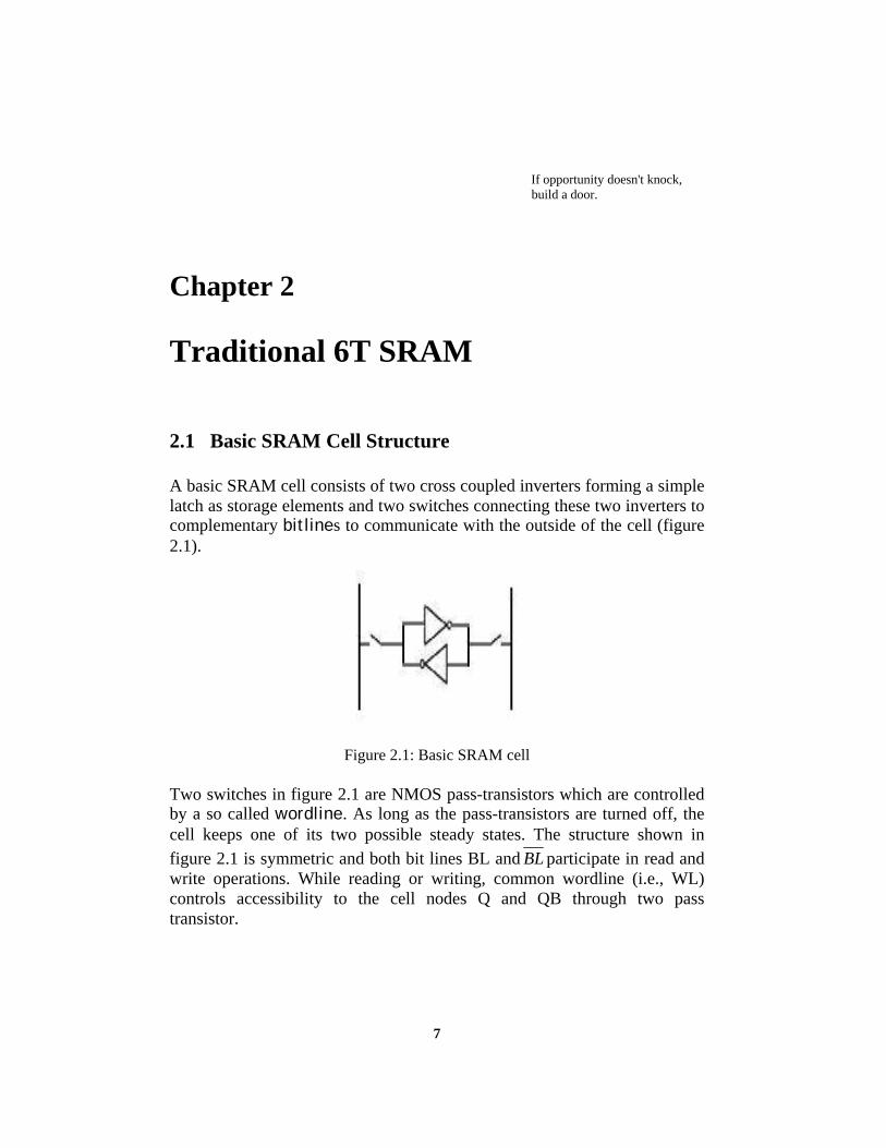
A basic SRAM cell consists of two cross coupled inverters forming a simple latch as storage elements and two switches connecting these two inverters to complementary bitlines to communicate with the outside of the cell (figure 2.1).
Figure 2.1: Basic SRAM cell
Two switches in figure 2.1 are NMOS pass-transistors which are controlled by a so called wordline. As long as the pass-transistors are turned off, the cell keeps one of its two possible steady states. The structure shown in figure 2.1 is symmetric and both bit lines BL and BL participate in read and write operations. While reading or writing, common wordline (i.e., WL) controls accessibility to the cell nodes Q and QB through two pass transistor.
7
8 Traditional 6T SRAM
Besides the 6 transistors, it requires the signal routing and connections to two bitlines (figure 3.2), a wordline (also called row address), and both supply rails. Placing the two PMOS transistors in the N-well also significantly consumes large area. Therefore, the SRAM cell should be sized as small as possible to obtain large memory densities. However, reliable operation of the cell enforces some sizing restrictions. The sizing strategy of the cell transistors is illustrated while read and write operations are described.
Figure 2.2: 6-transistor cell
SRAM cells are usually used to implement high capacity memories that require low power consumption, short access times, and endurance to process variations and environmental conditions. To write a value into an SRAM cell, the new value and its complement are loaded onto the bitlines by write circuit and the wordline is raised simultaneously. To read a value from an SRAM cell, both bitlines are precharged high and the wordline is raised turning on the pass transistors. The bitline relative to the cell node that contains 0 begins discharging. The sense amplifier, which is connected to the bitlines, detects which of the bitlines is discharging and hence reads the stored value. For deep understanding of the memory cell function, it is essential to describe the read and write operation in sequence. For this purpose, the overall function is explained through timing diagram. Assume a ‘1’ is stored at node Q and we want to read that value. Initially, both bitlines are prechared high, and after a short time, WL and read is asserted. Since QB side of the cell contains ‘0’, the left bitline begins to discharge (see timing
2.1.1 Read Operation 9
diagram). As a slight voltage difference between two bitlines is formed and detected by sense amplifier, the read value is ready at Dout output. Similarly, to write a ‘0’ into the cell, WL and write signals are asserted and the right bitline is forced to 0 and the left bitline is forced to 1 simultaneously, with strong write buffers (see timing diagram). After a short delay both node values are flipped and a ‘0’ value is written at Q.
Figure 2.3: Timing diagram of read ‘1’ and write ‘0’ operations
2.1.1 Read Operation
Assume that we want to read ‘1’. This means a 1 is stored at Q or implicitly a 0 is stored at QB. Furthermore, assume that both bitlines are precharged to 1V before the read operation to be initiated. The read cycle is started by asserting the wordline, enabling two pass-transistors M 5 and M 6 (see figure 3.2). Consequently, the contents stored at Q and QB begin to transfer to the bitlines BL and BL respectively. It is obvious that BL remains at its precharge value and no discharge happens. However, BL will be pulled down to the ground by discharging through M 5 -M 1 . A careful attention should be paid in sizing of transistors to prevent unexpected writing a 0 into the cell.
BL
WL
read/write
Dout read 1
Discharging
RE WE
data 0
Force BL to 1
Q 1
0 write 0 QB
BL Force BL to 0
10 Traditional 6T SRAM
This is illustrated in figure 2.4. Consider the BL side of the cell. The capacitance of the bitline for larger memories is significant. Upon enabling the WL, initially BL stays in its precharged value V DD . The path composed of M 5 -M 1 pulls down the bitline towards ground. As we would like to have a minimum size cell, these transistors should be chosen as close to minimum as possible, which cause slow discharge of bitline capacitance. Immediately when a small difference is created between the potentials of two bitlines, the sense amplifier becomes active to accelerate the read process.
Figure 2.4: Simplified cell during read operation. (Read ‘1’)
At the beginning, when the wordline is rising, the intermediate node between two NMOS transistors, QB, is pulled up toward the precharge value of bitline, BL . This voltage rise must be kept as low as possible with careful sizing of transistors not to cause sufficient current derive through M 3 -M 4 inverter, which may cause flip in the cell state. To avoid this from happening, the resistance of pull-down transistor, M 1 , must be less than that of pass transistor M 5 . This can be quantitatively obtained by solving the current equation at the maximum allowed value of voltage rise at node QB, which is the transistor threshold (of about 0.3 V). In other words, having less resistance for M1 , it must be stronger than access pass transistor. This means that the following relation must be satisfied.
1)(L
W ⟩ 5)(LW
Assuming M 1 as minimum size transistor, the access pass transistor M 5 has to be made weaker by increasing its length. This is undesirable, because it adds to the capacitance of bitline. Hence, it is favorable to minimize the size
2.1.1.1 Sense Amplifier 11
of M 5 and increase the width of pull-down M 1 to fulfill the stability requirements. Prior analysis considers the worst case condition in order to take into account the sever stability issues. In practice, the second bitline BL keeps Q close to V DD which makes unexpected toggling of the cross-coupled inverters more difficult. This demonstrates one of the major advantages of symmetrical cell that uses dual bitline architecture [4]. 2.1.1.1 Sense Amplifier One of the major issues in the design of SRAMs is the memory access time (or speed of read operation). For having high performance SRAMs, it is essential to take care of the read speed both in the cell-level design and in the design of a clever sense amplifier. Sense amplifiers are one of the most critical circuits in the periphery of CMOS memories [11]. Their performance strongly influences both memory access time and overall memory power consumption. High density memories commonly come with increased bitline parasitic capacitances. These large capacitances slow down voltage sensing and makes bitline voltage swings energy-consuming, which result in slower more power hungry memories. Need for larger memory capacity, higher speed, and lower power dissipation impose trade offs in the design of sense amplifier: - Increase in number of cells per bitline increases the bitline parasitic capacitance - Decreasing cell area to integrate more memory on a single chip reduces
the current that is driving the heavily loaded bitline. This causes smaller voltage swing on the bitline.
- Decreased supply voltage lead to smaller noise margin that affects the sense amplifier reliability.
Figure 2.5 demonstrates a typical use of a sense amplifier. Each column is connected to a single sense amplifier circuit and the corresponding column is selected by a column decoder. To read a memory cell the corresponding row (wordline) and column must be selected using periphery circuits called row and column decoders.
12 Traditional 6T SRAM
Figure 2.5: Read operation and sense amplifier [12]
Summarily, the main roles of sense amplifier are amplification of small voltage swing (voltage difference of bitlines) in large bitline, delay reduction, and power dissipation reduction by reducing large voltage swing. To accelerate the reading time, SRAMs use sense amplifiers. As the difference in voltage between bitlines becomes sufficient, the sense amplifier is activated and rapidly discharges one of the bitlines. Initially the sense amplifier is turned off (SE is low). As the bitlines of 6T cell are precharged high, so are the cross-coupled inverters of sense amplifier. At the same time the bitlines are equalized (EQ is low) so that any mismatch between them is balanced. Afterwards the wordline of the corresponding cell is asserted and simultaneously the EQ and PC are disabled to discontinue the precharging. The column selector CS is then lowered to connect the bitlines to the latch of sense amplifier [6]. CS signal determines the column which is connected to the sense amplifier. After some time, when sufficient voltage difference is built between the two inverters of the sense amplifier, the sensing becomes enabled by asserting SE (Sense Enable) and consequently connecting the source of NMOS transistors in the latch to GND. As the internal nodes of sense amplifiers are precharged high, the NMOS transistors are turned on, flowing current from those nodes to GND.
2.1.2 Write Operation 13
Figure 2.6: Sense amplifier [6] The node with higher initial voltage causes the opposite NMOS drive current faster. This will make the node having lower voltage drops faster, and in turn shut of the NMOS drawing current from the higher node. Therefore, an increased voltage difference is developed and eventually the nodes will flip to a stable state. Each output node, Out orOut , is connected to a buffer with the same size as inverters of sense amplifier. This is to ensure that the two sense amplifier nodes have the same load, and hence will be fully symmetric. It is worthwhile to mention that in traditional 6T SRAM cell it is ‘0’ that is detected by sense amplifier as the cell node containing ‘1’ is left unchanged. ‘0’ on the normal storage node results in a ‘0’ at the output of sense amplifier while a ‘0’ in inverse storage node results in ‘1’ [6].
2.1.2 Write Operation
Assume that we would like to write “0” and a 1 is stored in the cell (Q = 1). A correct write operation can be guaranteed with accurate consideration of device constraints. Similar to read operation, a write cycle is initiated by asserting WL with a slight delay. To write 0 into the cell the corresponding bitline, BL, is set to 0 and the other bitline, BL , is set to opposite value (i.e. 1). This causes the inverters to flip and change the state of the cell, provided to proper sizing of the transistors.
14 Traditional 6T SRAM
Figure 2.7: Simplified model of the cell during write initiation (writing 0 into the cell)
Assuming the write buffers to be strong enough, the write time is dominated by the propagation delay of the cross-coupled inverter pair. During the commencement of a write, the schematic of the cell can be simplified as Figure 2.7. It is reasonable to suppose that the gates of transistors M1 and M 4 remain at V DD and GND respectively. As long as the switching has not occurred, the mentioned assumption is true. Otherwise, the model demonstrated in Figure 2.7 is no longer valid and hence it is only useful to drive quantitative dc current equation in order to estimate the sizing of M 4 -
M 6 series combination. The hand-analysis solution gives a good insight to the estimation of device size. Moreover, accurate measurement can be carried out in the Integrated Circuits (IC) design tools such as Cadence. It is worthwhile to mention that due to sizing constraint imposed by read stability, the QB side of the cell cannot be pulled high enough to ensure the writing of 1 and it actually prevents the wanted write operation. In other words, the sizing constraint for read stability ensures that the potential of QB kept less than the threshold voltage of M 3 . Hence, a reliable writing of the cell is guaranteed through transistor M 6 if we can pull the node Q low enough, which is below the threshold voltage of M 1 . Looking at the right side of the cell, we have the series combination of M 4 -M 6 . Bitline, BL, is enforced to the ground. As the wordline is asserted, the pass transistor M 6 is turned on and current is flown from the cell storage node. Simultaneously, the pull-up PMOS transistor, M 4 , is turned on and, as soon as the node potential faces more voltage drop, further current will flow from V DD to GND. So M 6 has to be stronger than M 4 to change the state of the node
2.1.2.1 Write Circuitry 15
faster. As PMOS transistor due to lower mobility than NMOS, it is intrinsically weaker than the NMOS transistor. Therefore, taking both transistors minimum size implicitly means that NMOS is stronger and makes write operation possible. As a result, a 6T SRAM cell, shown in figure 2.2, requires accurate device sizing to balance read stability, write margin, and data retention in hold mode. Pull-down NMOS is made stronger than pass-transistor to obtain good read stability by minimizing the read upsets. Although a strong pull-up PMOS improves the read stability, it degrades the write margin. So, to achieve a good write margin, a sufficient pass-transistor is required [5]. Eventually, after study of the read and write operations and device physical constraints for read stability, write margin, and data retention, we demonstrate the sizing of the 6T SRAM cell in figure 2.7. This sizing has been approved by several simulations in Cadence in extreme process corners and validated by Monte Carlo Analysis with the presence of mismatch, process and temperature variation. Subsequently, in the future sections, we will discuss more elaborately about different process corners and supply voltage scaling and, there, we will clarify the importance of cell sizing in order to fulfill both area criteria for high capacity memories and reliability of cell arrays to meet the yield requirement.
Figure 2.7: Traditional 6T SRAM cell with size in 90nm Technology
2.1.2.1 Write Circuitry The write circuit is a simple differential stage which is driven by two Data and Write signals. The Data and Data is passed through write buffers and
16 Traditional 6T SRAM
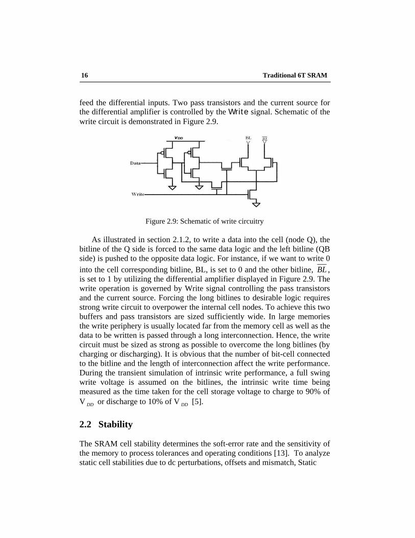
feed the differential inputs. Two pass transistors and the current source for the differential amplifier is controlled by the Write signal. Schematic of the write circuit is demonstrated in Figure 2.9.
Figure 2.9: Schematic of write circuitry As illustrated in section 2.1.2, to write a data into the cell (node Q), the bitline of the Q side is forced to the same data logic and the left bitline (QB side) is pushed to the opposite data logic. For instance, if we want to write 0 into the cell corresponding bitline, BL, is set to 0 and the other bitline, BL , is set to 1 by utilizing the differential amplifier displayed in Figure 2.9. The write operation is governed by Write signal controlling the pass transistors and the current source. Forcing the long bitlines to desirable logic requires strong write circuit to overpower the internal cell nodes. To achieve this two buffers and pass transistors are sized sufficiently wide. In large memories the write periphery is usually located far from the memory cell as well as the data to be written is passed through a long interconnection. Hence, the write circuit must be sized as strong as possible to overcome the long bitlines (by charging or discharging). It is obvious that the number of bit-cell connected to the bitline and the length of interconnection affect the write performance. During the transient simulation of intrinsic write performance, a full swing write voltage is assumed on the bitlines, the intrinsic write time being measured as the time taken for the cell storage voltage to charge to 90% of V DD or discharge to 10% of V DD [5].
2.2 Stability The SRAM cell stability determines the soft-error rate and the sensitivity of the memory to process tolerances and operating conditions [13]. To analyze static cell stabilities due to dc perturbations, offsets and mismatch, Static
2.2.1 Analytical Derivation of Static Noise Margin 17
Noise Margin (SNM) simulations have become dominant method to assess the cell reliability in high density memories. The focus of cell stability or implicitly the SNM analyses of SRAM cells have mostly restricted to the simulations, however, some works discuss this through providing analytical expression. This work deals with the SNM of SRAM cell both from analytic as well as simulations point of view. The advantage of mathematical representation is that it explicitly expresses the SNM as function of different cell parameters such as supply voltages, precharge voltages, bitline voltages, and source voltages. 2.2.1 Analytical Derivation of Static Noise Margin Analytical modeling of SRAM cell stability is not an entirely new concept. First time, E. Seevinck, F.List and J. Lohstroh in 1987 characterized the cell robustness by modeling the SNM of back-to-back inverters of the SRAM cell. The SNM can be found analytically by solving the Kirchhoff equations and applying one of the mathematically equivalent noise margin criteria [14]. Assume that the right side of the cell shown in Figure 2.11 to be at level zero and the left side to be at level One. With this assumption, Figure 2.11 is simplified as Figure 2.10 in which the dotted devices are assumed to be inactive or non-conducting. In Figure 2.11, it can be proven that the transistors M1 , M 5 , and M 6 operate in the saturation region while M 3 operates in linear region. Explicit expressions for SNM of 6T cell is obtained by using the basic CMOS model equations with constant threshold voltages (equal for n and p-channel) and neglecting second-order effects such as mobility reduction and velocity saturation [13].
Figure 2.10: Schematic diagram of SRAM cell in read access with static-noise sources V n inserted
18 Traditional 6T SRAM
The MOS models which we use to analyze SNM are
I D = 21 β (V GS - V T ) 2
I D = β V DS ( V GS - V T -21
V DS )
in the saturated and linear regions, respectively.
SNM T6 =V T - (1
1+k
){
1)k(rr1
V112V TDD
++
++
−rr
-)21(1
22k
qrk
qr
qrk
VV TDD
++++
−}. (2.1)
where r = ratio = ad ββ q = ap ββ
V T = threshold voltage
k = ⎟⎠⎞
⎜⎝⎛
+1rr
⎭⎬⎫
⎩⎨⎧
−−++ 1
/11
22rs VVr
r
V s = VDD - V T
V r = V s - ⎟⎠⎞
⎜⎝⎛
+1rr
V T
From (2.1), it can be perceived that the SNM of 6T cell is a function of the cell dimensions appeared as r and q ratio, threshold voltage V T which is highly affected by temperature and process tolerances, precharged voltage V s . The detailed derivation is presented in appendix A. 2.2.2 Static Noise Margin Static Noise Margin is defined as the maximum value of dc disturbances that the cell nodes can tolerate before flipping its state. Static noise is dc disturbance such as offsets and mismatches due to processing and variations in operating conditions. In this work, only static-noise sources are taken into account. The SRAM cell should be designed such that under all circumstances, there would be some SNM to deal with the dynamic
2.2.2 Static Noise Margin 19
disturbances caused by alpha-particle incidences, crosstalk, supply voltage ripple, and thermal noise. Figure 2.11 demonstrates the schematic diagram for SNM Cadence simulations. To simulate the SNM of this memory cell, two bitlines and the wordline of the cell are kept at V DD . This SNM is also called read SNM and the mentioned set-up for simulation suits to the read operation (see also Figure 2.12). Two equal dc voltage sources, V N are placed between inverters indicating the dc noise sources. These voltages are swept from 0 to V DD /2 (i.e. 0.5 V) or more until the cell storage data flips.
Figure 2.11: Schematic diagram for SNM Cadence simulations
It has to be mentioned that the cell size depicted in figure 2.7 is the base of all Cadence dc and transient simulations through this chapter.
Figure 2.12: Simulation set-up for read SNM
20 Traditional 6T SRAM
The SRAM cell can also be represented by a latch composed of two inverters as displayed in Figure 2.13. The voltage sources V n are static noise sources. Since the storage cell and two series noise-sources are isolated from the bitlines (i.e. the cell holds the data and its complement), it is anticipated that the cell nodes sustain lower noises than during read access, where the pass transistors are turned on and the storage nodes are connected to the bitlines. Consequently, the noise margin is wider and V n sweeps larger range until the nodes voltages flip.
Figure 2.13: Cross-Coupled inverters
The voltage of the noise sources are swept from 0 to V DD /2 (i.e. 0.5 V) or more until the cell voltages flip. The voltage of the noise at which the nodes voltages change the cell logic states is referred to as static noise margin of the cell, and can be considered as the relative cell dc noise margin.
Figure 2.14: Cell data transitions due to two series voltage noise sources (N-fast P-slow, 110 C° , V DD = 1V)
2.2.2 Static Noise Margin 21
In Figure 2.14 the transition of cell voltages for supply voltage 1V and worst case conditions (FS corner and 110 C° ) has been plotted. It can be observed that around V n equal to 215mV both node voltages begin to flip. This means that the worst case read SNM in V DD =1V is 215mV. In appendix B, this plot for different supply voltage has been included. In order to estimate the stability of the data retention, the noise margin was examined in section 2.3.1 with the aid of analytic expression. In this part, however, a common graphical representation of SNM so called butterfly curve for a cell during read access and while holding data (un-accessed) is presented. Butterfly curve is composed of the voltage transfer curve (VTC) of one inverter and the mirrored voltage transfer curve of the other inverter (VTC 1− ) in a single plot. Neglecting the mismatch and variation inside the cell, the two VTCs are equivalent. In Figure 2.15 the VCTs of one inverter is plotted for both read access as well as the hold mode. Curves a and x are typical characteristic of the cell in hold and read mode respectively. They are used as reference for comparison purpose. In standby (hold mode) three curves (a,b,c) are characterized which show the impact of stronger inverter NMOS in b and weaker inverter NMOS in c with respect to the nominal curve a. At read (x,y,z), the loading effect of pass transistor, with the bitline precharged at V DD , shifts the low output voltage part of the characteristics upwards.
Figure 2.15: Worst-case (N-fast P-slow) hold and read transfer characteristics of the cell inverter at 110 Co for V DD = 1.0V
22 Traditional 6T SRAM
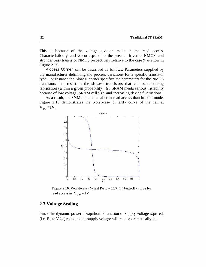
This is because of the voltage division made in the read access. Characteristics y and z correspond to the weaker inverter NMOS and stronger pass transistor NMOS respectively relative to the case x as show in Figure 2.15. Process Corner can be described as follows: Parameters supplied by the manufacturer delimiting the process variations for a specific transistor type. For instance the Slow N corner specifies the parameters for the NMOS transistors that result in the slowest transistors that can occur during fabrication (within a given probability) [6]. SRAM meets serious instability because of low voltage, SRAM cell size, and increasing device fluctuations. As a result, the SNM is much smaller in read access than in hold mode. Figure 2.16 demonstrates the worst-case butterfly curve of the cell at V DD =1V.
Figure 2.16: Worst-case (N-fast P-slow 110 Co ) butterfly curve for
read access in V DD = 1V 2.3 Voltage Scaling Since the dynamic power dissipation is function of supply voltage squared, (i.e. E d ∝V 2
DD ) reducing the supply voltage will reduce dramatically the
2.3 Voltage Scaling 23
dynamic power consumption. Hence scaling the supply voltage seems to be a necessary task. As the supply voltage V DD decreases from its nominal 1V in 90nm technology, noise margin decreases (Figure 2.17).
Figure 2.17: Noise margin versus V DD for read access TT typical, FS N-fast P-slow process corners
Table 2.1
Read SNM for different supply voltages (TT typical, FS N-fast P-slow worst case) at 110 C°
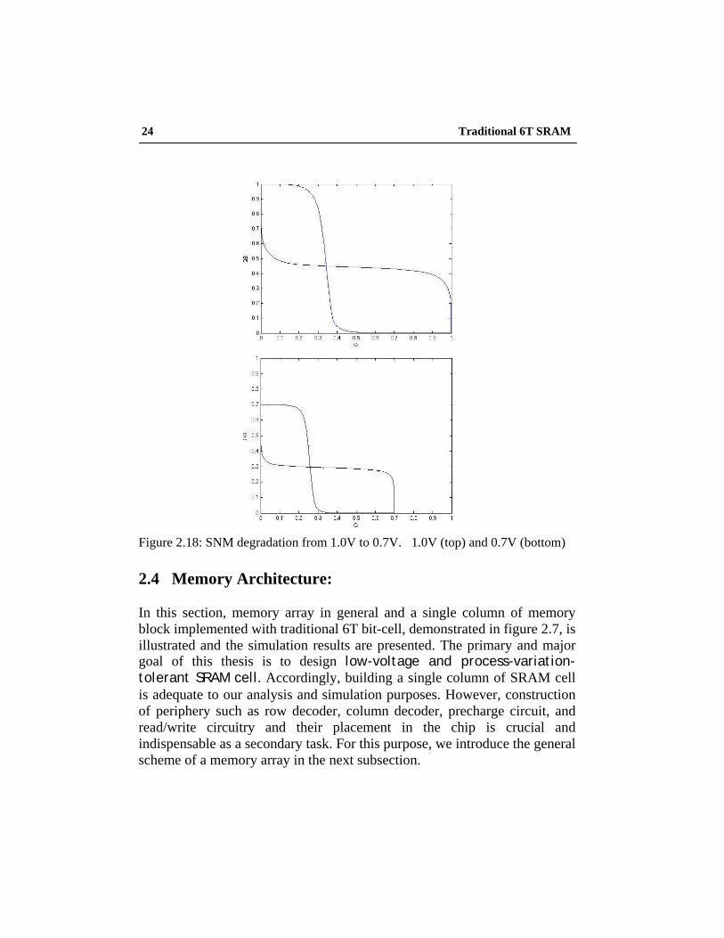
Since many disturbance signals are related to the V DD value, it is interesting to analyze the SNM butterfly curve for different supply voltage in worst-case condition. N-fast P-slow corner at highest temperature is the worst-case condition in traditional 6T cell (Figure 2.18).
24 Traditional 6T SRAM
Figure 2.18: SNM degradation from 1.0V to 0.7V. 1.0V (top) and 0.7V (bottom)
2.4 Memory Architecture: In this section, memory array in general and a single column of memory block implemented with traditional 6T bit-cell, demonstrated in figure 2.7, is illustrated and the simulation results are presented. The primary and major goal of this thesis is to design low-voltage and process-variation-tolerant SRAM cell. Accordingly, building a single column of SRAM cell is adequate to our analysis and simulation purposes. However, construction of periphery such as row decoder, column decoder, precharge circuit, and read/write circuitry and their placement in the chip is crucial and indispensable as a secondary task. For this purpose, we introduce the general scheme of a memory array in the next subsection.
2.4.1 General SRAM Structure 25
Subsequently, for the sake of simplicity, a single memory column implemented in Cadence and the related simulation results will be presented. 2.4.1 General SRAM Structure A general SRAM block and its peripheral circuits are displayed in Figure 2.19. The SRAM array consists of compact rows and columns of bit cells. For small caches, it is possible to place a word of data in a row, however, in large memories because of space limitation, it is necessary to arrange several words of data in each row. Cells of each column share the same bitlines. Before the read access, the bitlines are precharged to a known value by the precharge circuits. The row decoders are used to select a row in the array. Depending on the mode of operation, storage cells in the row are connected the common bitlines and either the stored data in the cell is read by sense amplifiers or overwritten by the write circuits.
Figure 2.19: General SRAM structure [15]
For larger memories, multiple blocks of the same array are used such that an extra address generator called block address decoder is required.
26 Traditional 6T SRAM
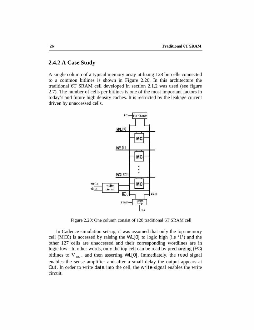
2.4.2 A Case Study A single column of a typical memory array utilizing 128 bit cells connected to a common bitlines is shown in Figure 2.20. In this architecture the traditional 6T SRAM cell developed in section 2.1.2 was used (see figure 2.7). The number of cells per bitlines is one of the most important factors in today’s and future high density caches. It is restricted by the leakage current driven by unaccessed cells.
Figure 2.20: One column consist of 128 traditional 6T SRAM cell In Cadence simulation set-up, it was assumed that only the top memory cell (MC0) is accessed by raising the WL[0] to logic high (i.e ‘1’) and the other 127 cells are unaccessed and their corresponding wordlines are in logic low. In other words, only the top cell can be read by precharging (PC) bitlines to V DD , and then asserting WL[0]. Immediately, the read signal enables the sense amplifier and after a small delay the output appears at Out. In order to write data into the cell, the write signal enables the write circuit.
2.4.2 A Case Study 27
The write circuit then drives the bitlines to known states depending on the data value.Figure 2.21 displays the simulation result for two consecutive read-write. The same plot for V DD = 0.7V appended to appendix B (figure B.6).
Figure 2.21: Simulated SRAM read and write operations (two consecutive read- write functions), V DD = 1.0V, FS corner and 110 C° .
The write operation, to some extent, is similar to the read operation. The cell is accessed with enabling wordline. The bitlines is driven to known
28 Traditional 6T SRAM
states by the write circuitry. The write circuitry is designed to have stronger current driving capability than the the precharge and storage cell circuitry such that to overpower the cell nodes. The same plot for V DD = 0.7V appended to appendix B (figure B.7).
Figure 2.22: Simulated SRAM write operation (FS corner and 110 C° ). Three consecutive write 1-0-1. The plot in Figure 2.22 is a snapshot of simulation used to verify the functionality of the SRAM cell in worst case temperature and process corner.
2.5 Low-Voltage SRAM Cells 29
The first three signals are control signals. Write signal activates the write mode. WL selects the top row to be accessed and data is the value to be written to the cell. The voltage of the bitlines is plotted next followed by the voltages of the cell nodes Q and QB. The simulation snapshot shows three consecutive writes cycles, write 1, 0, and 1 respectively.
2.5 Low-Voltage SRAM Cells By varying the supply voltage and clock frequency on demand, dynamic voltage scaling tries to provide high performance when it is required and low energy consumption during period of standby. Since the dynamic energy is a function of supply voltage squared, (i.e. E d ∝V 2
DD ) reducing the supply voltage will lower dramatically the dynamic energy consumption. High density sub-threshold SRAMs are indispensable in ultra-low power applications such as implantable devices, medical instruments, and wireless sensor networks [8]. The following subsections will review the previous most recent research in reducing the supply voltage. 2.5.1 8T Sub-V t SRAM Cell [3]
The sub-threshold regime is a critical biasing space since it enables minimum energy operation for logic circuits [2]. However, practical systems rely extremely on SRAMs which conventionally restrict the minimum V DD to above Vt. SRAMs often dominate the total die area and power, and minimizing their energy requires scaling V DD as low as possible [3]. In this work, a SRAM cell operating at sub-V t (at 350 mV) is presented. Although, the 6T bit-cell has a good balance between stability (read and hold SNM), performance, and density, yet in the presence of variations it fails to function in sub-V t . As demonstrated in Figure 2.23, at 350 mV, the hold SNM is preserved but read failures are significant. This figure displays read and hold SNM for three points (mean, 3δ , and 4δ ) versus supply voltage varying between 0.2 V and 1.0 V. The worst-case SNM in hold mode happens for 4δ at 0.3 V, which is slightly positive. This means that the hold
30 Traditional 6T SRAM
stability is preserved. However, at the same point, the read SNM is completely disappeared.
Figure 2.23: 6T cell SNM [3]
From above figure it can be realized that due to process variation the read stability is degraded in voltages below 0.7V and the cell fails to function at lower voltages. To overcome these challenges, [3] presents the 8T bit-cell shown in Figure 2.24.
Figure 2.24: 8T cell enabling low-voltage read/write and sensing [3]
2.5.1 8T Sub-V t SRAM Cell 31
The read buffer composed of transistors M 7 -M 8 eliminates the read SNM restriction, mentioned above, and make it possible to read the cell at 350 mV. In standard 6T bit-cell, in sub-V t , the values stored in unaccessed cells can lead to accumulated leakage current on the shared bitlines that limit the number of cells connecting to the same bitlines. In the proposed technology, this defect is resolved with a foot-driver periphery. As shown in Figure 2.25, instead of connecting the foot of read buffers directly to ground, a foot-driver is used in periphery. The buffer-foots of all bit-cells in the same word (all cells in the same row with the shared wordline) is shorted and use shared foot-driver. During a read, only the foot of the accessed word is driven low; all others remain at VDD. Therefore, after RDBL is precharged, the read buffers of unaccessed cells have no voltage drop across them, and their access transistor has negative V GS . As a result, they impose no sub-V t leakage.
Figure 2.25: Peripheral circuitry to eliminate sub-V t leakage
from unaccessed read buffers [3].
32 Traditional 6T SRAM
The write operations fail when the pass transistors cannot overcome the internal cell feedback. In this design, write is performed by boosting WL by 50mV and, more importantly, reducing VVDD through a supply driver (Figure 2.26). At the same time, new value is written by pulling the desired storage node low through the NMOS pass transistor.
Figure 2.26: Cell write performed by weakening local feedback. Cell supply settles to low intermediate voltage determined by supply driver and write drivers [3].
2.5.2 10T Sub-V t SRAM Cell It was mentioned in the previous section that due to reduced static noise margin (SNM) in the read mode (see Figure 2.23), weak writability, limited
2.5.2 10T Sub-V t SRAM Cell 33
number of cells per bitline as a result of accumulated leakage current in unaccessed cells connected to the same bitline, and reduced bitline sensing margin, the conventional 6T SRAMs in sub-threshold region fail to deliver the density and yield requirements. 10T SRAM cell proposed in this work improves the SNM by decoupling the cell nodes (using read buffer) from the bitline and making the read SNM comparable to that of hold SNM [9]. In this work, several circuit techniques are proposed for high density and robust sub-V t SRAMs as follows:
1. Decoupled cell by introducing read buffer for read margin improvement
2. Utilizing Reverse Short Channel Effect (RSCE) for write margin improvement
3. Eliminating data-dependent bitline leakage to enable long bitlines 4. Virtual ground replica scheme to improve bitline sensing margin Figure 2.27 displays the proposed 10T SRAM cell in two states, when the cell contains 1 and 0 respectively. When read is enabled (RWL=1), the read bitline, RBL, is discharged through M 7 , M 8 , M 9 depending on the value of QB.
Figure 2.27: Proposed 10T SRAM cell when store ‘1’ and ‘0’ [8]
34 Traditional 6T SRAM
This means that if QB is 1 (or implicitly the cell contains a 0 at Q), then all pull down transistors (M 7 , M 8 , M 9 ) are turned on and the RBL is discharged. Otherwise, there is no direct path through those transistors from RBL to the ground as M 8 is turned off. Accordingly, the cell node is isolated from the bitline during the read operations, maintaining the hold SNM. So, through this method (i.e. decoupled cell) the read margin in sub-V t is improved to a value roughly equal to hold margin. Figure 2.28 compares the SNM for 10T cell with that’s of conventional 6T cell at supply voltage of 0.2V. The SNM margin for 10T cell is 76 mV with respect to the 6T cell, which is only 14 mV. Moreover, it is shown in the Figure 2.27 that in unaccesed cells (RWL = 0), node A is maintained at VDD causing the leakage current flow from node A to RBL, regardless to the data stored in the SRAM cell. This method eliminates the data-dependent bitline leakage and consequently enables long bitlines. The leakage path has been marked in the Figure 2.27.
Figure 2.28: SNM comparison between conventional 6T and proposed 10T SRAM cells [8]
Similar to the 6T bit-cell, write operation is performed by asserting WWL and loading the data onto WBL and WBLB (Figure 2.26). To improve
2.5.2 10T Sub-V t SRAM Cell 35
write margin, write operation in the technology suggested in previous section is performed by boosting WL by 50mV and reducing VVDD through a supply driver (see Figure 2.26). Instead, this work utilizes the RSCE in sub-threshold region to improve the writability without introducing additional high VDD. RSCE is observed in modern CMOS devices due to the HALO pocket implants used to compensate the V t roll-off [10] [16]. As demonstrated in Figure 2.29, the pass transistors M 3 and M 6 utilize RSCE in order to refine write margin.
Figure 2.29: M 3 and M 6 utilize RSCE for write margin improvement [8] The proposed 10T SRAM cell eliminates the data-dependent bitline leakage by making M10 (see Figure 2.27) turned on in unaccessed cells while M 7 and M 9 is turned off (RWL =0). The drain voltage of M10 forces the leakage current always flow from the node A to bitline, regardless of stored data. To achieve higher sensing margin in sub-threshold region, a single-ended static-inverter read buffers (in contrast to differential Sense Amplifier) are applied as shown in Figure 2.30. In addition, a virtual ground replica scheme is proposed in this work to reach the highest sensing margin by utilizing a duplicate bitline composed of hardwired data and control signals, depicted as VGND Gen block. This technique makes the trip point of the read buffers
36 Traditional 6T SRAM
stay at the middle of the bitline high and low levels offering an ideal sensing margin [8]. At 0.2V supply a bitline swing of 130mV is obtained and the VGND block generates the highest logic ‘0’ voltage (midpoint), which becomes the virtual ground for read buffers.
“Simplicity of character results from complexity of thought. Judge the people regarding the questions they would ask, not the answers they may give.”
Chapter 3 Proposed SRAM Technology: Asymmetric 6T Cell 3.1 Basic Cell Structure A basic asymmetric 6T cell consists of two cross coupled inverter forming a simple flip flop as storage element and two switches connecting these two inverters to complementary bitlines (RBL and WBL) in order to communicate with outside of the cell (figure 3.1).
Figure 3.1: Basic asymmetric 6T SRAM cell
37
38 Proposed SRAM Technology
At the first glance, it looks like to the traditional 6T cell, however, there are a lot of differences in the structure of two cells. These differences are:
1- Read bitline (RBL) is separate from write bitline (WBL). This means that the read operation is performed independent of the right side bitline, unlike the traditional 6T cell which uses both bitlines simultaneously for read access and write operation. 2- Read wordline (RWL) is separate from write wordline (WWL). This means that for read access the new cell only asserts RWL to enable the left switch pass transistor and the right pass transistor is kept off. This is opposite to conventional 6T cell which uses both pass transistors by asserting common WL for read or write operation. Hence, the read access is performed only through the left side of the cell using RBL precharged high and then asserting the RWL. On the other hand, the write operation is accomplished only through the right side of the cell by enforcing the WBL to the desired value and then asserting the WWL, independent of the the left side. Whit this structure the symmetric topology of old 6T cell is no longer satisfied. 3- Unlike the traditional 6T cell that has two similar and equal size
inverters, in the invented cell the inverter marked II in figure 3.1 is stronger than the inverter I. In other words, this capability facilitates the read operation with the aid of the strong inverter while the write operation also experiences a weak inverter (Inverter I).
The new cell exploits the completely asymmetric topology in contrast with the symmetric 6T SRAM cell. The asymmetric feature proposed in the invented cell provides interesting properties. In the later subsections we try to enumerate them and illustrate them very thoroughly. Before going through our investigations in depth, we illustrate the read and write operations and give an insight to the cell sizing strategies. Simultaneously the read and write periphery are described. Consequently, the cell stability is discussed. In section 3.3 the potential of the cell functionality in very low voltages is illustrated. Eventually, in the end a memory array composing of AS-6T cells will be investigated.
3.1.1 Read Operation 39
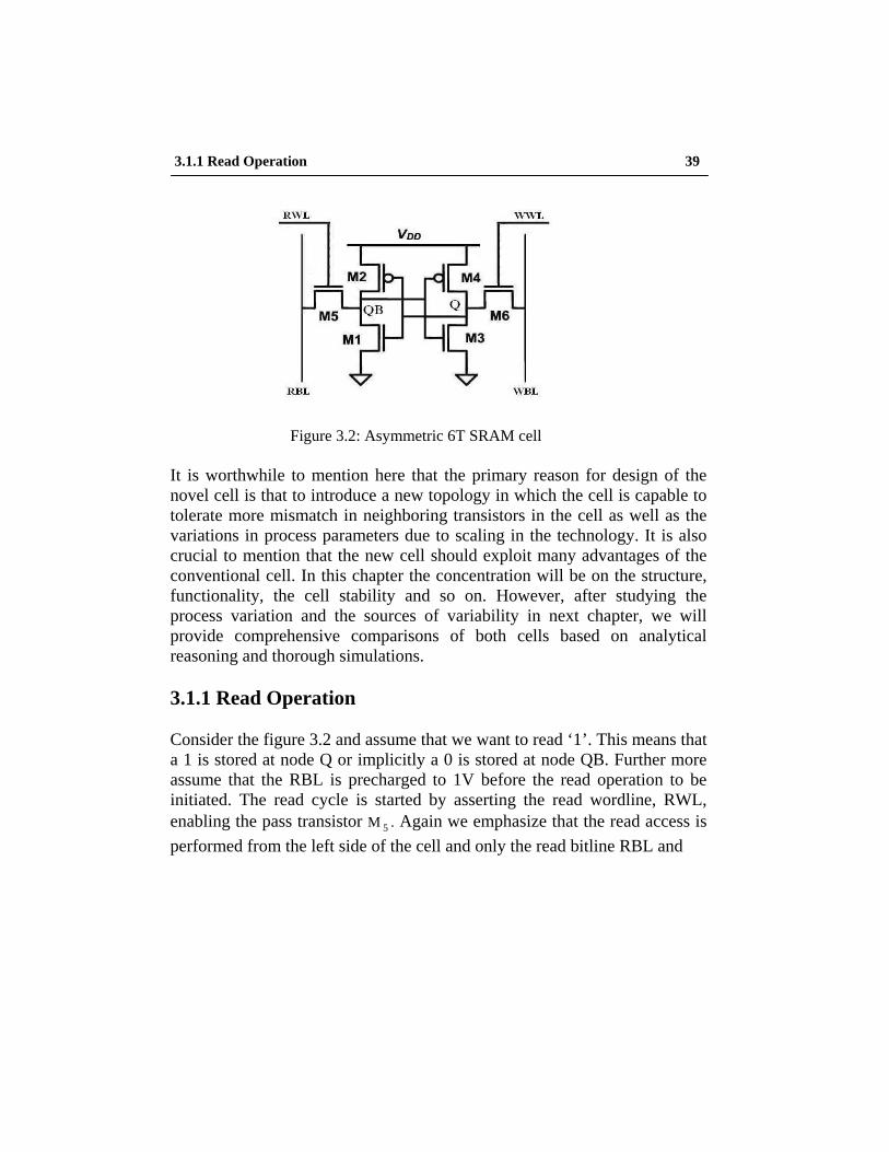
Figure 3.2: Asymmetric 6T SRAM cell It is worthwhile to mention here that the primary reason for design of the novel cell is that to introduce a new topology in which the cell is capable to tolerate more mismatch in neighboring transistors in the cell as well as the variations in process parameters due to scaling in the technology. It is also crucial to mention that the new cell should exploit many advantages of the conventional cell. In this chapter the concentration will be on the structure, functionality, the cell stability and so on. However, after studying the process variation and the sources of variability in next chapter, we will provide comprehensive comparisons of both cells based on analytical reasoning and thorough simulations. 3.1.1 Read Operation Consider the figure 3.2 and assume that we want to read ‘1’. This means that a 1 is stored at node Q or implicitly a 0 is stored at node QB. Further more assume that the RBL is precharged to 1V before the read operation to be initiated. The read cycle is started by asserting the read wordline, RWL, enabling the pass transistor M 5 . Again we emphasize that the read access is performed from the left side of the cell and only the read bitline RBL and
40 Proposed SRAM Technology
read wordline RWL are contributed. Consequently, the content stored at node QB is transferred to RBL. In this case where a ‘0’ is located at QB, the RBL is beginning to discharge to the left node and the right node Q is left untouched because the pass transistor M 6 is turned off via WWL. A careful sizing should be done for transistor combination M 5 -M 1 to prevent unexpected writing. The SRAM cell storage node is conventionally supposed to be the right node. Hence when we refer to writing a value, it means that we want to write that value into the right node, not the left one.
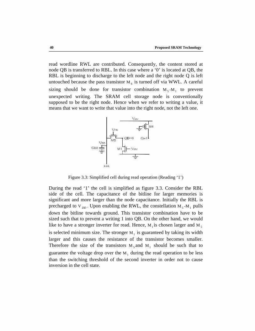
Figure 3.3: Simplified cell during read operation (Reading ‘1’)
During the read ‘1’ the cell is simplified as figure 3.3. Consider the RBL side of the cell. The capacitance of the bitline for larger memories is significant and more larger than the node capacitance. Initially the RBL is precharged to V DD . Upon enabling the RWL, the constellation M 5 -M 1 pulls down the bitline towards ground. This transistor combination have to be sized such that to prevent a writing 1 into QB. On the other hand, we would like to have a stronger inverter for read. Hence, M 1 is chosen larger and M 5 is selected minimum size. The stronger M 1 is guaranteed by taking its width larger and this causes the resistance of the transistor becomes smaller. Therefore the size of the transistors M 5 and M 1 should be such that to guarantee the voltage drop over the M 1 during the read operation to be less than the switching threshold of the second inverter in order not to cause inversion in the cell state.
3.1.2 Write Operation 41
Assuming supply voltage of 1V, M 5 operates in saturation region and M 1 operates in linear region. Then, neglecting the second-order effects the current equations in node QB can be written as:
21
nµ C ox5⎟⎠⎞
⎜⎝⎛
LW
( V 5GS - V tn ) 2 = nµ C ox1⎟⎠⎞
⎜⎝⎛
LW ( )
2(
2
1VVVV tnGS
∆−∆− )
V∆ is the voltage raise in node QB during the read operation. Solving above equation for V∆ gives a relationship in term of the cell ratio. The cell ratio is usually referred to as the ratio of the NMOS pull-down width to the width of pass transistor. From this we can reach to an analytical insight to the value of the cell ratio. Increasing the width of pass transistor can result in increase in the capacitance of the RBL. Thus, pass transistor is assumed to be minimum size and proportionally as we found at V∆ , the width of M1 is calculated. Although the computation of above analytic expression gives a good insight to the sizing of the cell transistors in the left side, the Cadence simulations for cell stability give accurate result. As soon as the voltage drop of the RBL line, during the discharge, reaches to a sufficient value that can be sensed by Sense amplifies, the sense amplifier is activated to accelerate the read process. As the read operation is not performed differentially like in traditional 6T cell, the single ended read amplifier is necessary instead of differential sense amplifier. It is essential to remark that when reading a ‘0’, the RBL experiences no discharging because the new constellation is created by M 5 and M 2 . Hence,
when no discharge happens, obviously the inverted value of the bitline appears at the output of the sense amplifier (see figure 3.4). 3.1.2 Write Operation Assume that we would like to write ‘0’ and ‘1’ is stored in the cell node (Q=1). Similar to read operation, the write cycle is initiated by asserting WWL with a slight delay. To write 0 the write bitline (i.e. WBL) is set to zero through the write circuitry (see figure 3.4). The write operation is performed only over the right side of the cell, unlike the traditional 6T cell
42 Proposed SRAM Technology
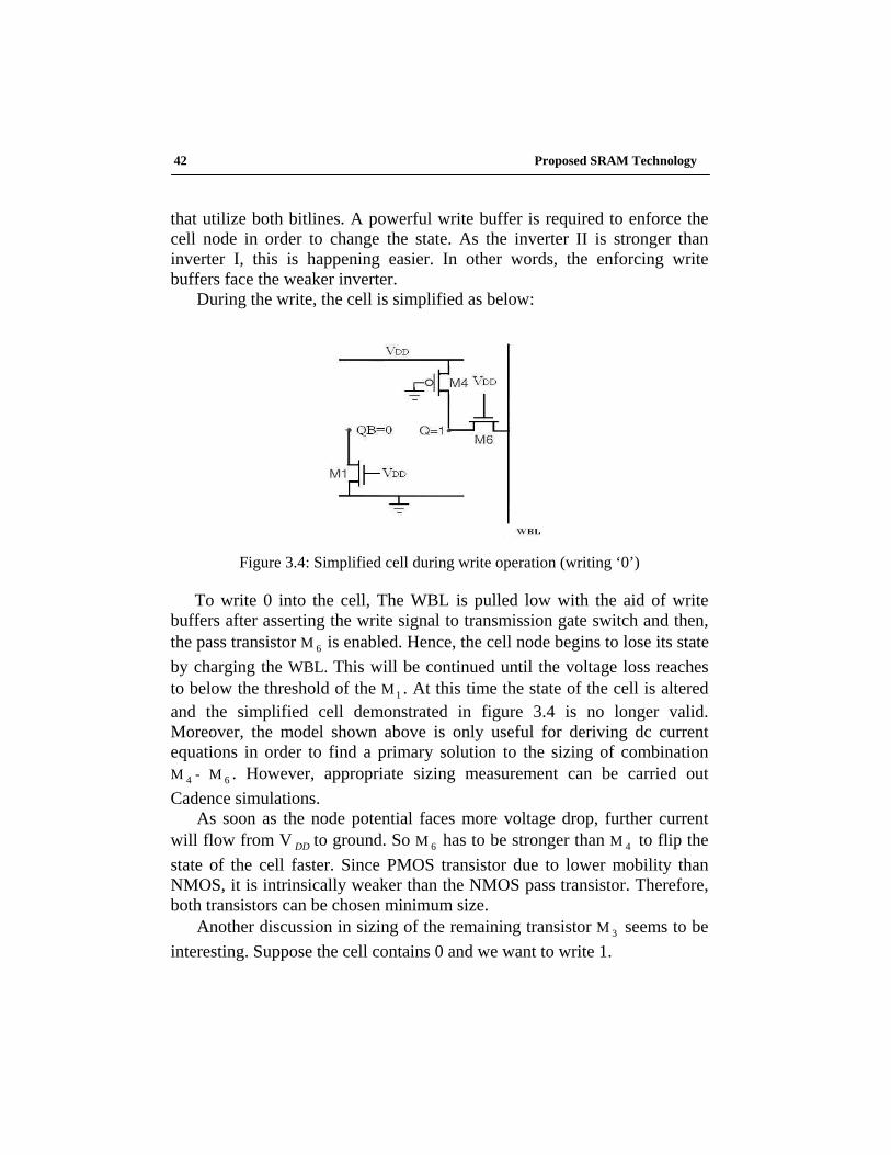
that utilize both bitlines. A powerful write buffer is required to enforce the cell node in order to change the state. As the inverter II is stronger than inverter I, this is happening easier. In other words, the enforcing write buffers face the weaker inverter. During the write, the cell is simplified as below:
Figure 3.4: Simplified cell during write operation (writing ‘0’)
To write 0 into the cell, The WBL is pulled low with the aid of write buffers after asserting the write signal to transmission gate switch and then, the pass transistor M 6 is enabled. Hence, the cell node begins to lose its state by charging the WBL. This will be continued until the voltage loss reaches to below the threshold of the M 1 . At this time the state of the cell is altered and the simplified cell demonstrated in figure 3.4 is no longer valid. Moreover, the model shown above is only useful for deriving dc current equations in order to find a primary solution to the sizing of combination M 4 - M 6 . However, appropriate sizing measurement can be carried out Cadence simulations. As soon as the node potential faces more voltage drop, further current will flow from V DD to ground. So M 6 has to be stronger than M 4 to flip the state of the cell faster. Since PMOS transistor due to lower mobility than NMOS, it is intrinsically weaker than the NMOS pass transistor. Therefore, both transistors can be chosen minimum size. Another discussion in sizing of the remaining transistor M 3 seems to be interesting. Suppose the cell contains 0 and we want to write 1.
3.1.2 Write Operation 43
See the simplified cell below.
Figure 3.5: Simplified cell during write ‘1’
Similarly, for writing 1 into the cell the WBL is pushed V DD through write buffers after asserting the write signal to transmission gate and then the pass transistor M 6 is enabled. Hence, the bitline is beginning to discharge. Then, the potential of the cell node is raised. Whenever, it reaches to threshold of M 1 the cell inverters are flipped and change the state. To preserve the cell stability, some sizing constraint is required. According to the above cell, M 6 and M 3 operates in saturation and linear regions respectively. Applying the kirchhof low at Q, neglecting the second-order effects the current equations can be written as:
21
nµ C ox6⎟⎠⎞
⎜⎝⎛
LW
( V 6GS - V tn ) 2 = nµ C ox3⎟⎠⎞
⎜⎝⎛
LW ( )
2(
2
3VVVV tnGS
∆−∆− )
Where V∆ is the voltage raise over M 3 . To change the state of the cell this value should be larger than the threshold voltage (~0.3). Then, solving the equation gives us a relationship in terms of ratio of both transistor dimensions. Given β = (W/L) 3 /(W/L) 6 , the above equation is reduced to
44 Proposed SRAM Technology
β = 2
)2(V ) V- V (
GS3
2tnGS6
VVVtn ∆−∆− (3.1)
Assume V DD =1V, tnV = 0.3V and minimum V∆ = 0.35V to cause flip in the cell state. Also regarding the values for tnV and V∆ , the values V 6GS and V 3GS are calculated 0.65 and 1V respectively. Replacing the parameters in (3.1) gives:
β = (W/L) 3 /(W/L) 6 =1/4 or (W/L) 6 = 4 (W/L) 3 (3.2) As previously mentioned, pass transistor M 6 is assumed to be minimum size. Then, the length of M 3 should be enhanced at least four times larger than minimum length to satisfy (3.2). The minimum acceptable length in 90nm technology is 0.1µ m. This hand-analysis calculation guides us to follow the same strategy for sizing along with simulations. Eventually, after study of the read and write operations and device physical constraints for read stability, write margin, and data retention, we demonstrate the sizing of the AS-6T SRAM cell in figure 3.6. This sizing has been approved by several simulations in Cadence in extreme process corners and validated by Monte Carlo Analysis in the presence of mismatch, process and temperature variations.
Figure 3.6: Proposed 6T SRAM cell with size in 90nm technology
3.1.3 Read and Write Circuitry 45
3.1.3 Read and Write Circuitry A simple scheme of read and write circuitry is shown in figure 3.7. In the read access (read signal assertion) depending on the cell stored value, RBL either remain non-discharged or begin to discharge. The latter happens when the cell contains 1. In this case, the RBL discharged and as soon as its voltage drop reaches to a sufficient level, the sense amplifier becomes active to accelerate the read process. As the read operation is not performed differentially like in traditional 6T cell, a single ended read amplifier is required instead of differential sense amplifier. As it can be seen in figure 3.7 the first buffer is supposed to be minimum size not load the bitline capacitance, however, the subsequent buffer is chosen highly strong to accelerate the read operation.
Figure 3.7: AS-6T cell accompany with single-ended read and write buffers The write operation is activated by asserting the write signal to enable the switch and then pushing the WBL to V DD or pulling the WBL to ground in the case or writing 1 or 0 respectively. The write buffers are given too strong to overpower the cell inverters as well as to accelerate the charging or
46 Proposed SRAM Technology
discharging the large bitline capacitance. 3.2 Cell Stability Stability was investigated elaborately and thoroughly in section 2.2 for standard 6T cell and static noise margin was computed both analytically and based on simulations. But, here we only suffice to cell schematic representation and simulation results. Figure 3.8 demonstrates the schematic diagram for SNM measurements in Cadence simulations. To simulate the SNM of this memory cell, the read bitline RBL and the read wordline RWL are kept at V DD . This SNM is also referred to as read SNM and the mentioned set-up for simulation suits to the read operation. Two equal dc voltage sources, V N are placed between inverters indicating the dc noise sources.
Figure 3.8: Schematic diagram for read SNM measurement in Cadence
simulations.
The SRAM cell can also be represented as figure 3.9 for hold (standby) SNM measurement.
Figure 3.9: AS-6T cell in hold mode
3.2 Cell Stability 47
The voltage of the noise sources are swept from 0 to V DD /2 until the cell voltages flop. The voltage of the noise at which the nodes voltages change the cell logic state is considered as relative cell dc noise margin.
Figure 3.10: Cell data transitions due to sweep in two series voltage noise sources at V DD = 1V in read access (worst case N-Fast P-Fast corner, 110 ° C) In above waveform plots the point at which two voltages intersect each other is the maximum tolerable dc noises that can be applied in the cell nodes to bring the cell to opposite state. Both two noise sources are increased uniformly in the same direction. In subsequent section when we discuss the scalability of AS-6T, the same simulations will be performed for different process corners. In appendix C, the same plot has been included for different supply voltages. The SNM is also can be measured using butterfly curves. SNM is defined as the side of the largest possible square which can be inscribed between VTC curves in butterfly characteristic. Neglecting the effect of mismatch and process variation, two virtual squares have approximately equal side in traditional 6T cell, However, in AS-6T it is not the case. This is evident from the butterfly curve. Thus, between the two squares surrounded, the SNM is assumed to be the side of the smaller one.
48 Proposed SRAM Technology
Figure 3.11: Worst-case (N-fast P-fast corner and 110 C° ) read SNM butterfly curve at V DD =1V 3.3 Voltage Scaling As we observed in chapter 2 for conventional 6T, the cell can operate until the edge of 0.7V (see Figure 2.23). Due to process variation the read stability is degraded in voltages below 0.7V and the cell fails to function at lower voltages. However, the AS-6T can operate in voltages below 0.7 since the cell in more tolerant to the process variation. In subsequent chapter, we will study the process variation and its sources and later in chapter 5, we will compare both cells in terms of their capability in voltage scalability as well as cell stability. Therefore, in this section, we partially consider the voltage nodes that the invented cell operates and also we present the simulation results in different voltage nodes. It is worthwhile to declare that we designed AS-6T such that it is able to operate until the edge of 0.7V since we want to compare both cells in voltage range from 0.7V to 1V. Subsequently, we demonstrate that the AS-6T cell is able to function in lower voltage than 0.7 with applying efficient sizing. Hence, the cell utilized below 0.7V is a bit larger and is able to work to the edge of 0.48V.
3.3 Voltage Scaling 49
The simulation of SNM measurement for different supply voltages listed in the next table was performed in different process corners. It can be easily recognized that the FF (Fast-NMOS Fast-PMOS) is the worst case whereas SS corner (N-Slow P-Slow) is the best case. All simulations were performed in the worst case temperature (i.e. 110 ° C).
Table 3.1: SNM measurement in different process corners at 110 ° C. SNM values are in mV.
As the supply voltage V DD decreases from its nominal 1V in 90nm technology, noise margin also will be reduced (figure 3.12).
Figure 3.12: Read noise margin versus V DD indicating FF corner the worst case and SS the best case process corner
50 Proposed SRAM Technology
3.4 Memory Architecture, a Case Study The general memory array architecture was presented in section 2.4.1. In our investigation over this thesis, we designed similarly a single column of a typical memory array utilizing 128 bit cells of AS-6T connected to common bitlines (figure 3.13). The number of cells per common bitlines is one of the most critical factors in the design of high density memories. This amount is restricted due to amount of leakage current flowed from bitline to cell nodes in unaccessed cells. In Cadence simulation set-up, it was assumed that only the top memory cell (MC0) is accessed by raising the RWL[0] to logic high (i.e ‘1’) to read the cell and raising the WWL[0] to write into the cell MC0 and the other 127 cells are unaccessed and their corresponding wordlines are in logic low. In the other words, only the top cell can be read by precharging (PC) bitlies to V DD , and then asserting RWL [0]. Immediately, the read signal enables the sense amplifier and after a small delay the output appears at Out. In order to write data into the cell, the write signal enables the write circuit. The write circuit then drives the write bitline (WBL0) to known states depending on data value.
Figure 3.13: One column consist of 128 AS-6T SRAM cells
3.4 Memory Architecture, a Case Study 51
The advantage of this columnar design is that 127 unaccessed cells dissipate leakage current. Thus, the simulations for read and write operations are valid in actual functioning condition. Figure 3.14 displays the plot of two consecutive write-read operations in worst case condition.
VDD= 1V, FF corner, 110 ° C. The plot in figure 3.14 is a snapshot of simulation used to verify the functionality of the SRAM cell. The first five signals are control signals. Write signal activates the write mode. WWL and RWL select the top row to be accessed and data is the value to be written to the cell.
52 Proposed SRAM Technology
The voltages of bitlines are plotted next followed by the voltages of the cell nodes Q and QB. The simulation snapshot shows consecutive write and read cycles. In the remaining part of this section, we concentrate on the voltage scalability of the proposed 6T cell. We will demonstrate with several simulations that the cell presented in figure 3.6 functions in lower voltages, to the edge of 0.49V, in the worst case process corner (i.e. FFA with ± 3σ ) and high temperature (i.e. 110 ° C). It has to be mentioned that the simulations were performed in 128 cells connected to common bitlines, which is the actual operating condition. Monte Carlo analysis because of large number of simulations and taking into account large amount of physical and environmental parameters is more accurate than the process corner analysis. Here, we only display the results for FFA corner in 0.5V and 0.45V respectively and we show that the cell fails to function in voltage lower than 0.5V.
Although we only concentrated on process corner analysis in this chapter, which is single point simulation, but in future after study of process variation in subsequent chapter and partly showing the Monte Carlo analysis results, we will present extensive and thorough simulations in chapter 5 while we compare the traditional and invented cells.
Figure 3.16: Write failure at t = 5ns and read failure at t = 10ns VDD= 0.45V, SFA (N-slow P-fast with ± 3σ ) corner, 110 ° C.
Above figure demonstrates that the first write operation starting at t = 4ns (see WWL rise) is failed and the cell nodes (see voltages Q and Qbar) cannot be overpowered by write circuit. Consequently, the cell with geometries shown in figure 3.6 does not function properly in voltages lower than 0.5V. In addition, new sizing strategy may be required to go to voltages below this level.
54 Proposed SRAM Technology
3.5 Improved AS-6T Cell In previous section, we demonstrated with simulation that the As-6T cell with sizing presented in figure 3.6 is not able to function in voltages below 0.5V. For this reason, we enhanced the cell with new size such that it is able to work properly in 0.43V. The new cell is very much larger than As-6T cell.
Figure 3.17: Enhanced As-6T cell with its dimensions in 90nm technology
3.6 Dual-V t AS-6T Cell According to SNM measurements listed in table 3.1, the worst case SNM of AS-6T cell in 0.7V is only 91mV while that of 6T cell is 155mV (see table 2.1). Utilizing the fact that the SNM increases with exploiting high V t transistors, we simulated the cell introduced in figure 3.17 with all various combinations of dual-V t transistors. Although choosing all transistors as high-V t significantly improves the cell stability, it also degrades the performance of read access as well as limits the voltage scalability of the cell. Therefore, a compromising solution is to utilize dual-V t transistors. In other words, we use some transistor with typical V t and the others with high-V t . Because of cell asymmetry, large combinations of dual-V t transistors can be tested. However, after exhaustive simulations the best case was chosen in which both PMOS pull-up transistors were selected as high-V t and all other transistors were selected as typical V t .
3.6 Dual-Vt AS-6T cell 55
With this combination we make a balance between read delay, voltage scalability as well as the cell stability. Dual-V t cell is able to function in 0.58V compared to improved AS-6T cell that could function in 0.43V. The worst case SNM of dual-V t cell measured by process corner analysis in various supply voltages listed in table 3.2.
Table 3.2: SNM measurement in different process corners at 110 ° C. SNM values are in mV.
If you live properly, the dreams will come to you.
Chapter 4 Study of Mismatch and Process Variation:
4.1 Introduction The impact of mismatch and process variation on SRAM yield (i.e. the number of non-faulty chips) has become a serious concern to continued scaled technologies [17]. While dimensions of MOSFET are increasingly scaled, microscopic variations in number and location of dopant atoms in the channel region of the device elevate limitations in the electrical deviations of device characteristics [18], [19]. These atomic-level intrinsic fluctuations cannot be eliminated by external control of manufacturing process and become more critical in the SRAM cells which commonly use minimum-geometry transistors [20]. Variations in transistor parameters of the SRAM cell such as threshold voltage, gate length, and channel width extremely degrade the static noise margin. Intrinsic fluctuations cause threshold voltage mismatch between the neighboring transistors. This mismatch creates more SNM degradation than the threshold voltage mismatch due to manufacturing-relevant variations.
57
58 Mismatch and Process Variation
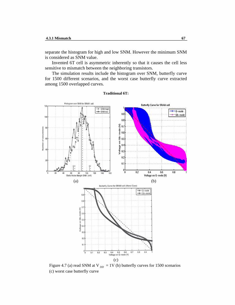
Variations in process parameters such as channel length, threshold voltage etc., is divided into two groups: intra-die variation and die-to-die variation. The intra-die (on-die) random variations result in mismatch in the strength between the neighboring transistors in the cell. The primary source of mismatch is the V t variations caused by random dopant fluctuations (RDF). These V t variations can produce read, write, access, and hold failures, so called parametric or functional failures, in an SRAM cell which consequently deteriorate the yield [21]. The threshold voltage variation due to random dopant fluctuation is inversely proportional to gate area. Because of this dependence, the minimum-size transistors commonly used in the cell are highly subjected to random fluctuations. Increase in the cell area or use of higher redundant columns (rows) improve the cell strength against intra-die variations. However, larger cell area and higher redundancy increase the leakage current and hence power dissipation in memory blocks. In addition, the die-to-die variation in transistor parameter (e.g. V t ) also has significant impact on the cell functional failures. For instance, the low-V t dies mostly suffer from read and hold failures while the high-V t dies suffer from write failures. Two techniques demonstrated in [21] present post-silicon adaptive solutions to a high extent mitigate the effect of process parameter variations in memory chips. There, the authors claim that post-silicon self-repair and self-adaptive techniques are crucial for designing low-power and process-variation-tolerant memories in sub-100nm nodes. A cell failure can originate from an increase in the cell access time (access failure), instability in the read or write operation (read/write failure), or failure in data retention at low supply voltages (hold failure). A failure in a row (or column) makes the row (or column) faulty. Whenever the number of faulty rows (columns) is greater than the number of redundant rows (columns), then the memory chip is faulty. Manufacturing variations can be categorized as systematic or random. Systematic variations are predictable intrinsically and depend on deterministic factors such as layout structure and surrounding topological environment [22] [23]. These factors can be managed during the cell-level design, memory array partitioning as well as interconnects.
4.2 Design Variability 59
On the other hand, random variations are unpredictable and are originated from random uncertainties in the fabrication process such as microscopic fluctuations in the number and locations of dopant atoms in the channel region [19] [24]. As a result, scaled technologies of VLSI circuits, particularly density-constrained memory requirements, can result in serious degradation in performance- and power-related parameters. These parameter degradations result in variability in the delay (e.g. access time) and power consumption of CMOS SRAMs. Therefore deterioration in device and interconnect parameter accuracy has intensified variability as the first-order challenge to the continued technology scaling. Hence, in order to efficiently exploit the benefits of scaling under process variations, not only the scaled technology nodes should provide the designer opportunities such as dual-V t or multiple- V t transistors but also the designer must employ new approaches such as bias control technologies to deal with the variation including parameter fluctuations [25].
4.2 Design Variability The variation in process parameters such as channel length, width, oxide thickness, and placement of dopants in the channel region result in a large variation in threshold voltage. Among those parameters, the random placement of dopants creates more concern because it causes threshold voltage mismatch between neighboring the transistors in the SRAM cell (intra-die variation). With scaling the number of dopant atoms varies and becomes lower. Fewer dopant atoms make V t control very difficult. 4.2.1 Source of Variability Atomistic-level differences between devices cause intrinsic variations, even though the devices have equal geometry and environment (systematic variation). In [26], an experiment shows the variability of threshold voltage. In this experiment, about 3500 identical n-MOSFETs positioned horizontally in a compact line and have been measured. Despite the fact that there is no systematic process variation between the FETs, relatively wide
60 Mismatch and Process Variation
gaussian distribution of threshold voltage has been obtained. Figure 4.1 shows this distribution in 90nm node.
Figure 4.1: Threshold voltage distribution for FETs in 90nm L= 46nm, W = 122nm
The V t shifts of the cell transistors due to random dopant fluctuations can be considered as independent Gaussian random variables with standard deviation given by [27]:
tVσ = effeff
dmsub
WLWN
3 tq
ox
ox
ε= 3.19 x 10 8− ⎣ ⎦
⎟⎟⎟
⎠
⎞
⎜⎜⎜
⎝
⎛V
WLN
effeff
A4.0
oxt
Where t ox is the oxide thickness, W dm is the width of the depletion region, N sub is the doping concentration in substrate, N A , L eff , and W eff are the average channel doping, channel effective length and width respectively. The WL1 dependency of
tVσ means more variations for smallest transistors, this dependency is recognizable from figure 4.2.
4.2.1 Source of Variability 61
As shown in figure 4.2, about 1500 different FETs for 32 different Length × Width combinations in compact arrays have been measured. The standard deviation,
tVσ , of each distribution has been extracted and is plotted to show the dependence of channel area [26].
Figure 4.2:
tVσ versus the (channel area) 5.0− . Each point is a different Length ×Width dimensions [26]
Figure 4.3 shows the threshold voltage distribution functions computed for each technology node using the input parameters listed in Table 4.1 from the roadmap, assuming minimum size and uniformly doped MOSFETs. It is clear on the figure that from 250nm to 50nm, the variation or deviation becomes wider. The standard deviations in threshold voltage for different nodes have been included as well.
Figure 4.3: Distribution density function for threshold voltage
for 1997 NTRS using models from [19]
62 Mismatch and Process Variation
Table 4.1
Input parameter for calculating threshold voltage due to intrinsic fluctuations [19]
The second significant source of variability, possibly is Line-Edge Roughness (LER). Atomistic-scale tolerances in doping levels and device feature sizes cause variation in source and drain region, influencing the overlap capacitance and the effective source resistance [26].These fluctuations cause random placements of dopant atoms demonstrated in figure 4.4 [30]. The gate edge is smooth in this figure, however, it is not usually the case because fluctuations in doping level cause uncertainty in the edges of source and drain, which directly relates to the S/D capacitance and resistance variations. LER aggravates this effect. LER arises from statistical variations in the number of incident photon during lithography exposure, the absorption rate, and chemical reactivity [31]. Similar LER roughness may happen along the gates of MOSFETs, making variability in effective gate length and width. The third source of intrinsic variability stems from atomistic-scale t ox (oxide thickness) variations. The gate oxide thickness is currently equivalent to about five inter-atomic spacings in the nanometer scaling. This thickness varies by one or two inter-atomic spacings which increase ~10% in overall σ V t [32]. In addition to three most significant source of variations just mentioned above, there are other kinds of sources that cause variability and hence affect the performance. Summarily, in sub-100nm nodes, variations mainly arise from: -Fluctuations due to manufacturing process (e.g., drifts in L eff , t ox ,V t , etc.) which extremely affect the circuit yield.
4.2.1 Source of Variability 63
- Environmental operating conditions such as supply voltage and temperature after the circuit is manufactured.
- Lack of proper modeling or accurate cell/transistor models
- Uncertainty or inaccuracy of simulation tools
Figure 4.4: (a) Randomly placed dopants in 50nm channel length MOSFET. The dense area contains donors creating source and drain. (b) Top view [30] More complete list of variability sources are listed in Table 4.2.
Table 4.2: Variability sources [29]
Process Variation Variation in Circuit
Operation Simulation Tools
Accuracy Channel Length Supply Voltage Timing Analysis
Channel Width Temperature RC Extraction
Threshold Voltage Aging (NBTI) Cell Modeling I-V Curves
Overlap Capacitance Cross-Coupling Capacitance
Circuit Simulations
Interconnect Multiple input Switching
Process Files
etc. etc. Transistor Models
64 Mismatch and Process Variation
4.2.2 SRAM Sensitivity SRAMs are the most sensitive to variations because almost the smallest applicable transistors are used in the cell to minimize the cell area, small signal analog levels are used together with logic level signals as well as the time available to sense a cell’s state is commonly less than that is required to obtain full swing in the case of read operation. The latter is most critical because in the analysis of delay in the read access, the variability cause shifts in time and consequently affects the performance. The most important parameter in the cell transistors affected by variations is threshold voltage. Alteration in doping level in the channel, channel width, channel length, and gate oxide thickness cause variation in threshold voltage. Accordingly, variation in threshold voltage directly influences current, noise, power dissipation, and the speed of the cell. It is worthwhile to mention the threshold voltage can also change if the source of the cell is not connected to ground (body effect).
∆ V t = k ( −− Bf Vφ2 fφ2 ) (4.1)
4.2.3 Process Variation Tolerant Design
4.2.3.1 Self-repairing SRAM The reliance of V t to body bias voltage introduces an opportunity to the design of process variation tolerant (PVT) SRAMs [21] referred to as self-repairing SRAM that uses leakage monitor and body-bias to simultaneously improve parametric yield and reduce leakage spread. The main advantage of this technique is that it presents a dynamic and adaptive post silicon solution to improve the SRAMs yield. In the self-repairing SRAM, the leakage of the SRAM array is monitored through Online Leakage Monitor (OLM). The Online Leakage Monitor is placed between the Supply voltage and the SRAM array as it can be seen in figure 4.5. Normally this block is bypassed via a calibrate signal. The OLM block produces an output voltage (V out ) which is proportional to the leakage of the array. This voltage is compared with two reference voltages (V 1ref and
4.2.3 Process Variation Tolerant design 65
Figure 4.5: Self-repairing SRAM [33] V 2ref ) using two voltage comparators. The reference voltages correspond to the different on-die process corners. Based on the comparison, the Body- Bias Generator (BBG) applies proper body bias to the SRAM array. For instance, if the SRAM die is in its low on-die V t corner, the generated V out will be greater than both reference voltages and both comparators produce zero, resulting in use of reverse body bias (RBB). Figure 4.6 demonstrates reduction in amount of failures in 256KB memory array.
Figure 4.6: Reduction in number of failures in 256KB memory array [33]
66 Mismatch and Process Variation
4.3 Monte Carlo Analysis
Monte Carlo analysis was performed on both traditional 6T cell and the proposed asymmetric 6T cell to find the mean and standard deviation of SNM. The histogram over SNM as well as the butterfly curve has been generated by Monte Carlo analysis. For each cell, 1500 scenarios for each supply voltage in the range (from 0.7V to 1.0V), each temperature (27 or 110 C° ), and read access or hold mode were performed. For instance, to generate histogram over SNM of a cell in V DD of 1V at 27 C° for read access, 1500 scenarios were simulated. Additionally, to produce a SNM butterfly curve of a cell in V DD of 0.7V at 110 C° in hold mode (standby), 1500 various scenarios were simulated. Therefore, with these two examples, it is obvious that because of very different conditions in operating supply voltages, worst-case temperatures as well as read/hold case for histogram graph and SNM butterfly curve, there are enormous number of simulations to validate the results. The Monte Carlo simulations have been performed for traditional 6T cell and the invented cell for both mismatch and process-variation separately. Therefore, an unimaginable amount of simulations have been accomplished in order to verify the functionality of both cells as well as the sensitivity of both cells to mismatch and process variations. The exhaustive simulations continually took about 72 hours. Partly in this chapter and more thoroughly in next chapter the conventional and the invented cells will be compared in terms of mismatch and process variations. The simulation set-up has been performed in Cadence using an ocean file (.ocn file) and the histogram and butterfly curves were extracted among the data stored through Monte Carlo simulations using MATLAB script for both invented and new cells. The ocean file as well as the MATLAB script for each cell is separately included to the appendix D and E. 4.3.1 Mismatch In 6T cell there is a relative symmetry in transistors dimension and bitlines during read and write accesses. However, because of physical mismatch between neighboring transistors, the cell slightly loses the symmetry. It is evident from the histogram over SNM in which both plots are not fully overlapped. This is also can be recognized in butterfly curve in which both eyes are not completely the same size. For this reason we
4.3.1 Mismatch 67
separate the histogram for high and low SNM. However the minimum SNM is considered as SNM value. Invented 6T cell is asymmetric inherently so that it causes the cell less sensitive to mismatch between the neighboring transistors. The simulation results include the histogram over SNM, butterfly curve for 1500 different scenarios, and the worst case butterfly curve extracted among 1500 overlapped curves.
Traditional 6T:
(a) (b)
(c)
Figure 4.7 (a) read SNM at V DD = 1V (b) butterfly curves for 1500 scenarios (c) worst case butterfly curve
68 Mismatch and Process Variation
The figure 4.7 (a) shows the number of cells in term of their SNM values. The dashed and solid histograms correspond to side of each square inscribed in eyes of butterfly. Because of relative symmetry in the cell, these histograms are approximately identical. The mean value is 87mV and all 1500 cells are stable during read access. Figure 4.7 (c) shows the worst case butterfly extracted among 1500 curves in figure 4.7(b).
Proposed 6T:
(a) (b)
(C)
Figure 4.8 (a) read SNM V DD = 1V (b) butterfly curves for 1500 scenarios (c) worst case butterfly curve
4.3.2 Mismatch and Process Variation 69
4.3.2 Mismatch and Process Variation The simulation results include the histogram over SNM, butterfly curve for 1500 various scenarios, and the worst case butterfly curve extracted among 1500 overlapped curves.
Traditional 6T:
(a) (b)
(c)
Figure 4.9 (a) read SNM at V DD = 1V (b) butterfly curves for 1500 scenarios (c) worst case butterfly curve The figure 4.9 (a) shows the number of cells in term of their SNM values. The dashed and solid histograms correspond to side of each square inscribed
70 Mismatch and Process Variation
in eyes of butterfly. Because of relative symmetry in the cell, these histograms are approximately identical. The mean value is 70mV and a large amount of cells are unstable during read access (having negative SNM) and fail to be read correctly. This can also be observed in the worst case butterfly curve in figure 4.9 (c) in which the eyes of curve completely vanish.
Proposed 6T:
(a) (b)
(c)
Figure 4.10 (a) read SNM at V DD = 1V (b) butterfly curves for 1500 scenarios (c) worst case butterfly curve
4.3.2 Mismatch and Process Variation 71
Figure 4.10 (a) shows the number of cells in term of their SNM values. The dashed and solid histograms correspond to side of each square inscribed in two eyes of butterfly shown in figure 4.10 (b). Unlike traditional 6T cell because of full asymmetry, these histograms are different. According to smaller eye in figure 4.10 (c), corresponding histogram has less SNM mean value. The mean values are 135mV and 335mV for higher and lower SNM respectively, however, the minimum of these two values is considered as read SNM. As it can evidently be observed in figure 4.10 (a), all 1500 cells have positive SNM and compared to traditional 6T (see figure 4.9.a) the read access for all cells is successful. Consequently, proposed 6T cell is more tolerant to mismatch and process variation than traditional 6T cell. This also can be noticed in the worst case butterfly curve in figure 4.10(c) in which a small eye is present in lower part of curve. From the histograms displayed in figures 4.9.a and 4.10.a, standard deviation for traditional 6T and proposed 6T cells are 45mV and 48mV respectively.
72 Mismatch and Process Variation
“Live your life as simple as you are.” Warren Buffet
Chapter 5 Overall Comparison The 6T bit-cell has a good balance between stability (read and hold SNM), performance, and density, yet in the presence of variations it fails to function in sub-V t . As demonstrated in Figure 2.23, at 350 mV, the hold SNM is preserved but read failures are significant. This figure displays read and hold SNM for three points (mean, 3δ , and 4δ ) versus supply voltage varying between 0.2 V and 1.0 V. The worst case hold SNM in happens for 4δ at 0.3 V, which is slightly positive. This means that the hold stability is preserved. However, at the same point, the read SNM is completely disappeared. 5.1 Voltage Scalability In chapter 2 and 3 for traditional 6T and proposed 6T cells, the voltage scaling was extensively illustrated. Here we only suffice to the lowest functioning supply voltage for both cells.
73
74 Overall Comparison
(a)
(b) Figure 5.1: Cell operating condition in lowest possible functioning supply voltage (a) 6T (b) AS-6T Process variation in 6T cell cause 6T cell to operate in voltages lower than 0.7V as shown in figure 5.1 (a). However, proposed cell is able to function to the edge of 0.5V (figure 5.1.b).
5.2 Stability 75
5.2 Stability The investigation of cell stability for conventional 6T and proposed 6T cells were discussed in chapter 2 and 3 respectively. According to process corner analysis the worst case static noise margin were listed in table 2.1 and table 3.1 and they are repeated below for worst case process corner, FS for 6T and FF for AS6T, and 110 ° C temperature.
Table 5.1 Read SNM in different operating supply voltages
V DD (V) 1.0 0.9 0.8 0.7
6T 215 198 179 155 AS-6T 96 96 95 91
5.3 Mismatch and Process Variation The effect of mismatch and process variation on different cells (6T and AS-6T) was partly shown in section 4.3. There, we only displayed the simulation results for read access in 1V supply voltage. However, in this section we present more thoroughly the simulation results of Monte Carlo analysis both in read access and hold mode.
(a) (b)
Figure 5.2: Histogram over read SNM in 0.7V (a) 6T (b) AS-6T
76 Overall Comparison
According to histograms shown in figure 5.2 proposed 6T cell is more variation-tolerant than traditional 6T. As it can be observed from left figure, lots of 6T cells have negative SNM and hence are considered as read failures. Mean and standard deviation for 6T cell is 52mV and 38mV respectively. Where as the mean and standard deviation for AS-6T cell are 117mV and 40mV respectively. The right figure shows that all 1500 cells under experiment have positive SNM. Therefore no read failures happen.
(a) (b)
Figure 5.3: Worst case read SNM butterfly in 0.7V (a) 6T (b) AS-6T From butterfly curves shown in figure 5.3 for both cells it is fully obvious that the 6T butterfly has no eye while that of AS-6T has a small eye. This means that AS-6T cell is stable during read access in 0.7V while 6T is unstable. In the rest of this section, the simulation results of hold mode for both cells are compared.
5.3 Mismatch and Process Variation 77
(a)
(b)
Figure 5.4: Histogram over hold SNM in 0.7V (a) 6T (b) AS-6T
78 Overall Comparison
(a) (b)
Figure 5.5: Worst case hold butterfly in 0.7V (a) 6T (b) AS-6T
According to figures 5.4 and 5.5, it can easily be noted that both cells are stable in the hold (unaccessed) mode, however, 6T cell has larger SNM than AS-6T.
Chapter 6 Future Work 6.1 Chip Fabrication and Evaluation In this thesis, we introduced a new technology in the design of low-voltage SRAM memory cell. We presented both theoretical background as well as simulations and demonstrated by several simulations that the proposed SRAM technology is fully functional in lower voltage than the standard 6T SRAM cell. Furthermore the new cell tolerates more local and global tolerances than the conventional 6T SRAM. Subsequently, as the next step, it is extremely worthwhile to fabricate the memory array architecture presented in chapter 3 to evaluate the chip by accurate post-layout simulations and measurements. Therefore, it is crucial to demonstrate that the chip is functional both in simulations as well as in real world. 6.2 Design of Ultra Low-voltage Asymmetric 6T SRAM Cell Several research work have been accomplished in very low-voltage 6T SRAM. Some works currently have been reported in sub-threshold operation. In this thesis, it was demonstrated that the asymmetric 6T cell is capable of functioning in low voltages. There is no doubt that the operation in subthershold region is the most critical challenge for today and future high performance, large capacity, and ultra low-power cache. To perform this, we suggest applying secondary and additional supply voltage by boosting wordline and, more importantly, reducing virtual V DD through a supply driver illustrated in section 2.5.2. Moreover, the cell array architecture presented in [34] for conventional 6T memory arrays can be
79
80 Future Work
extended to the asymmetric 6T cell array. This work represents a memory architecture with the aid of header and footer circuits by utilizing virtual V DD and virtual GND to improve writability. Additionally, In the proposed cell, the write and read operations are performed independently such that the read operation is performed by the left-side bitline while the write operation is performed using the right-side bitline independent of the read bitline, However, the asymmetric cell can share both bitlines during the write. Probably, this can improve writability of the cell or even refine the supply voltage scalability to the lower operating voltage. Therefore, additional hardware logic can be added for each row of the memory array such that can control the read and write accesses. In the write access, both pass transistors have to be activated by asserting the read and write wordlines simultaneously. Whereas the read operation utilizes only the left-side bitline and in this case only one pass transistor has to be activated by asserting only the read bitline. To deal with this, a multiplexer which select between two possible inputs can be used. One input to the multiplexer is the read wordline (RWL) signal while the other input is the and-gated of both read wordline (RWL) and write wordline (WWL). Operation in ultra low-voltage era may be achieved with the expense of additional hardware overhead for each row of memory array. 6.3 Study of Leakage Power in Asymmetric 6T SRAM Cell The SRAM leakage power dissipation has become a serious concern in high capacity SRAM memories. To efficiently use the chip area, it is crucial to reduce the leakage dissipation in SRAM memory. Reduction of leakage will result in increase in number of cells that share common bitline and therefore, it directly affects the area-efficiency. 6.4 Study of Static Noise Margin in Sub-V t Asymmetric 6T SRAM Cell Although many efforts have been performed in developing of criteria to analyze the SRAM cell stability such as cell loop gain, and static noise margin, those techniques and analyses can be extended to the new asymmetric cell. With the technology scaling the cell SNM is degraded. One
6.4 Study of Static Noise Margin 81
solution of improvement in SNM value is to utilize dual-V t transistors in the structure of the cell, however, using high V t transistors aggravate the read access time and scalability of supply voltage. Therefore, making compromise becomes necessary in balancing between the read delay, voltage scaling and higher SNM. In this thesis some of different combinations of high-V t and low-V t transistors (so called dual-V t transistors) were used and several simulations have been accomplished. Consequently higher SNM was achieved. However, the read delay degradation has not been investigated. To do this, a careful study of read periphery and clever design of sense amplifier is required.
References: [1] S. Manne, A. Klauser, and D. Grunwald, ”Pipeline gating: Speculation control for energy reduction,” in Proc. 25th Annu. Int. Sym. Computer Architecture, 1998, pp. 32-141. [2] A. wang, A. Chandrakasan, and S. Kosonocky, “Optimal Supply and Threshold Scaling for sub-Threshold CMOS circuits.” Proc. IEEE Comp. Society Annual Int. Symp. VLSI pp. 5-9. Apr., 2002 [3] N. Verma, A. Chandarkasan, “A 65nm 8T Sub-Vt SRAM Employing Sense- Amplifier Redundancy” ISSCC 2007 [4] Digital Integrated Circuits by Jan M. Rabaey, Anantha Chandrakasan, and Borivoje Nikolic [5] K. Zhang, U. Bhattacharya, Z. Chen, F. Hamzaoglu, D. Murray, N. Vallepalli, Y. Wang, B. Zheng, and M. Bohr, “SRAM Design on 65-nm CMOS Technology With Dynamic Sleep Transistor for Leakage Reduction” [6] Ingvar Carlson, “Design and Evaluation of High Density 5T SRAM Cache for Advanced Microprocessors” Linkoping University, Reg nr: LiTH-ISY-EX- 3481-2004 [7] B. Cheng, S. Roy, A. Asenov, “The Scalability of 8T-SRAM Cells under the Influence of Intrinsic Parameter Fluctuations,” 37th European Solid State Device Reseach Conference, 2007. ESSDERC [8] Tae-Hyoung Kim, Jason Liu, John Keane, Chris H. Kim, “A High-Density Subthreshold SRAM with Data-Independent Bitline Leakage and Virtual Ground Replica Scheme”, ISSCC 2007 [9] B. H. Calhoun and A. Chandrakasan, “A 256 Subthreshold SRAM Using 65nm CMOS,” ISSCC Tech. Degest, pp. 628-629, Feb., 2006 [10] Tae-Hyoung Kim, Hanyong EomJohn Keane, Chris H. Kim, “Utilizing Reverse Short Channel Effect for Optimal subthreshold Circuit Design,” University of Minnesota [11] Y. Tsiatouhas, A. Chrisanthopouus, et al.”New memory sense amplifier designs in CMOS technology”, IEEE, 2000 [12] ICE, “Memory 1997” [13] E. Seevinck, F. List, J. Lohstroh, “Static-Noise Margin Analysis of MOS SRAM Cells”, JSSC 1987, PP. 748-754. [14] J. Lohstroh, E. Seevinck. and J. de Groot, “Worst-case static noise margin criteria for logic circuits and their mathematical equivalence,” IEEE J. Solid- State Circuits, vol. SC-18, no. 6, pp. 803-807, Dec.1983. [15] Design of the RAM arrays used in Aries, Ecole Polytechnique Federale de Lausanne, Switzerland http://si2.epfl.ch/~gurkayna/aries/all.html [16] B. Yu, E. Nowak, K. Noda, and C. Hu, “Reverse Short Channel Effects and Channel-Engineering in deep-Submicron MOSFETs: Modeling and Optimization,” Symp. VLSI Technology, pp. 162-163, Jun., 1996.
82
References 83
[17] K. Agrawal and S. R. Nassif, “Statistical Analysis of SRAM Cell Stability,” In Procc. Of IEEE/ACM DAC, pages 57-62, 2006. [18] R.W. Keyes, “The effect of randomness in the distribution of impurity atoms on FET threshold,” App. Phys., vol. 8, pp.251-259, 1975 [19] X. Tang, V. De, j. Meindl, ”Intrinsic MOSFET parameter placement due to random placement “, IEEE Trans on VLSI, 1997, pp. 369-376. [20] D. Burnett, K. Erington, C.Subramanian, and K. Baker, “Implications of fundamental threshold voltage variations for high-density SRAM and logic circuits,” in Proc. Symp. VLSI Tech., June 1994, pp. 15-16. [21] S. Mukhopadhyay, S. Ghosh, K. Kim, and K. Roy, ”Low-Power and Process Variation Tolerant Memories in sub-90nm Technologies”. [22] M. Orshansky, L. Milor, P. Chen, K. Keutzer, C. Hu, ”Impact of systematic spatial intra-chip gate length variability on performance of high speed digital circuits”, ICCCAD 2000, pp.62-67. [23] V. Mehrotra et al. “A methodology for modeling the effects of systematic within-die interconnect and device variation on circuit performance”, DAC, 2000, pp. 172-175. [24] R.W. Keyes, “The impact of randomness in the distribution of impurity atoms on FET threshold”, Journal of Applied Physics, 1975, pp. 251-259. [25] Bhavnagarwala A, Kosonocky S, Radens C, Stawiasz K, Mann R, Ye Q, etal. Fluctuation limits and scaling opportunities for CMOS SRAM cells. Tech. Digest IEDM; 2005. p. 659-62. [26] K. Bernstein, D. J. Frank, A. E. Gattiker,W. Haensch,B. L. Ji, S. R. Nassif, E. J. Nowak, D. J. Pearson, N. J. Rohrer, ”High-performance CMOS variability in the 65-nm regime and beyond ”, 2006 IBM. [27] A. Bhavnagarwala, et. al.,“The impact of intrinsic device fluctuations on cMOS SRAM cell stability,” IEEE J. Solid State Cicuits, vol 36, no. 4, pp. 658-665, April 2001. [28] S. Mukhopadhyay, et. al., “Modeling and estimation of failure probability due to parameter variations in nano-scale SRAMs for yield enhancement,” Symp. on VLSI Circuits, 2004, pp. 64-67, June 2004. [29] A. Alvandpour, “VLSI Test Principles and Challenges”, Electorinic Devices, Department of Electrical Engineering, Linkoping University, 2007. [30] D. J. Frank, H. S. Wong, ”Simulation of Stochastic Doping Effects in Si MOSFETs,” Proceedings of the International Workshop on Computational Electronics, 2000, pp. 2-3. [31] T. brunner, “Why Optical Lithography Will Live Forever,” J. Vac. Technol. B21, No. 6, 2632-2637, 2003. [32] A. Asenov, A. R. BrownJ. H. Davies, S. Kaya, and G. Slavcheva, “Simulation of Intrinsic Parameter Fluctuations in Decananometer and Nanometer-scale MOSFETs,” IEEE Trans. Electron Devices 50, 1837 (2003).
84 References
[33] S. Mukhopadhyay, K. Kang, H. Mahmoodi, and K. Roy, “Design of Reliable and Self-Repairing SRAM in Nano-scale Technologies Using Leakage and Delay Monitoring” [34] B. Zhai, D. Blaauw, D. Sylvester, and S. Hanson, “A Sub-200mV 6T SRAM in 0.13µ m”, ISSCC 2007.
Appendix: A Derivation of SNM for Conventional 6T Cell [13] For the circuit of figure A.1 we assume that M 1 and M 6 to be saturated and M 2 and M 3 to operate in the linear region. These assumptions were checked by simulation and back substitution of the result. Equating the drain currents of M 1 and M 2 and those of M 3 and M 6 , and using the models in A1 and A2 result in
I D = 21 β (V GS - V T ) 2
I D = β V DS ( V GS - V T -21
V DS ) (A2)
Figure A.1: Schematic diagram of SRAM cell in read access with static-noise sources V n inserted
(V 1GS - V T ) 2 = )
21 V(2
2T22 DSGSDS VVVrq
−− (A3)
(V 6GS - V T ) 2 = ) 21 V(2
3T33 DSGSDS VVVrq
−− (A4)
85
86 Appendix A: Derivation of SNM for Conventional 6T Cell
Where the threshold voltage of the p- and n-channel devices are assumed equal and q = ap ββ , r = ad ββ .
The required Kirchhoff voltage equations are
V 1GS = V n + V 3DS (A5) V 2DS = V DD - V n - V 3GS (A6)
V 2GS = V DD - V n - V 3DS (A7) and V 6GS = V DD - V 3DS (A8) Substituting these into (A3) and (A4) yields
(V 3DS + V n - V T ) 2 = rq
(V DD - V n - V 3GS )
.(V S -V T -V n -2V 3DS +V 3GS ) (A9)
(V S -V 3DS ) 2 = 2rV 3DS ) 21 V( 3T3 DSGS VV −− (A10)
With V S = V DD - V T , as before. Eliminating V 3GS or V 3DS from these two equations results a fourth-degree equation which is too complicated to be useful. A simplifying approximation leading to a lower degree is therefore necessary. The transfer characteristic of the inverter which is ON has a relatively constant slope around its operating point. In figure A.2, this part of the characteristic is shown, together with a straight-line approximation through point P at V 3GS = V S which is the approximate operating point when marginal noise is applied. The linear approximation is defined by the value of V 3DS and its slope at point P. V 3DS at point P is derived from (A10) by substituting V 3GS = V S . The slope is determined by first differentiating (A10) with respect to V 3GS and then evaluating at V 3GS = V S . The required linear approximation is then expressed as (see figure A.2)
V 3DS =V 0 - KV 3GS (A11)
87
With
V r = V S - (1+r
r) V T (A12)
k = (1+r
r)
⎪⎭
⎪⎬⎫
⎪⎩
⎪⎨⎧
−−++ 1
/11
22rS VVr
r (A13)
and
V 0 = kV S + (krr
r/1
1+++
) V r . (A14)
Next we eliminate V 3DS from (A9) and (A11). After simplifying, we obtain
X 2 (1+2k+qr
k 2 ) + 2X(qr
kA + A + V T - V S ) + qr
A 2 = 0 (A15)
where, for simplicity, we have defined
X = c- V n - V 3GS A = V 0 + (k+1) V n - k V DD - c (A16)
Applying double-root stability criterion to (A15) and then substituting (A16), we solve for V n to obtain SNM:
SNM T6 = V T - (1
1+k
) {
1)k(rr1
V112V TDD
++
++
−rr
- )21(1
22k
qrk
qr
qrk
VV TDD
++++
−}. (A17)
88 Appendix B: Simulation Results for 6T
B: Simulation Results for 6T B.1: 6T, Process Corner Analysis In section 2.2.2, the method for measuring the SNM through process corner analysis was illustrated and data transitions due to applying two series noise sources (see Figure 2.12) was shown in Figure 2.14. In this section the same plot is displayed for supply voltages 0.9, 0.8, and 0.7 respectively for FS and TT process corners. FS and TT are the worst case and typical process corners respectively.
Figure B.1: Cell data transitions due to two series voltage noise sources (N-fast P-slow, 110 C° , V DD = 0.9V)
Figure B.2: Cell data transitions due to two series voltage noise sources (N-fast P-slow, 110 C° , V DD = 0.8V)
89
Figure B.3: Cell data transitions due to two series voltage
Figure B.6: Simulated SRAM read and write operations (two consecutive read- write) at V DD = 0.7V, FS corner, 110 C° .
91
Figure B.7: Simulated SRAM write operation. Three consecutive write 1-0-1 at V DD = 0.7V, FS corner, 110 C° .
C: Simulation Results for AS-6T C.1: AS-6T Cell, Process Corner Analysis
Figure C.1: Cell data transitions due to sweep in two series voltage noise sources at V DD = 0.9V in read access (worst case N-Fast P-Fast corner, 110 ° C)
92 Appendix C: Simulation Results for AS-6T
Figure C.2: Cell data transitions due to sweep in two series voltage noise sources at V DD = 0.8V in read access (worst case N-Fast P-Fast corner, 110 ° C)
Figure C.3: Cell data transitions due to sweep in two series voltage noise sources at V DD = 0.7V in read access (worst case FF corner, 110 ° C)
Figure C.4: Cell data transitions due to sweep in two series voltage noise sources at V DD = 0.7V in read access (Best case SS corner, 110 ° C)
93
D: Cadence Simulation File for Monte Carlo Analysis D1: Monte Carlo simulation set-up for 6T cell: ; Setup the sweep variables VDDlist = list(1.0 0.8 0.7) TempList = list(27 110) ; Setup the number of Monte-Carlo runs NoOfMCruns = 1500 StartIter = 1 sprintf(str_MCruns "%d" NoOfMCruns) sprintf(str_Iter "%d" StartIter) ; This part is included for future use when the sizes are included as variables ; SizeList = ... ; ---- ; Start sweep from here foreach(VDD VDDlist foreach(Temp TempList ; Setup the sweep variables WLlist = list(0 VDD) foreach(WL WLlist ;--------------------- simulator( 'spectre ) design("/tmp/aliye718/simulation/TB_6T_SRAMcell_DCsim_Q/spectre/schematic/netlist/netlist") resultsDir("/tmp/aliye718/simulation/TB_6T_SRAMcell_DCsim_Q/spectre/schematic" ) modelFile( '("/edu/aliye718/ST90nm/setupfile_typ_fast_slow.scs" "STAT") ) analysis('dc ?saveOppoint t ?param "VQ" ?start "0" ?stop VDD ?step VDD/200 ) desVar( "VWL" WL ) desVar( "VQ" 0 ) desVar( "vdd" VDD ) desVar( "VBLB" VDD ) desVar( "VBL" VDD ) temp( Temp ) save( 'i "/I0/M0/d" "/I0/M1/d" "/I0/M3/d" "/I0/M2/d" "/I0/M5/s" "/I0/M4/s" )
94 Appendix D: Cadence Simulation File for Monte Carlo Analysis
E: MATLAB Script E1: MATLAB Script for Monte Carlo Analysis for 6T cell: clear all close all % Define the amount of title rows in the data file and define the amount of Monte- % Carlo simulations that have been run. This will be used in order to reshape the % data files in the appropriate matrix format noTitleRow = 4; MCruns = 1500; noColumns = 1+MCruns; VDD = 1.0; % Open files fidQ = fopen('simResult/Sym_SRAM/MismatchProcessVar/MismatchSRAM_DC_Q_Vdd1000_Temp27_WL1000_Runs1500_Start1.txt','r'); fidQb = fopen('simResult/Sym_SRAM/MismatchProcessVar/MismatchSRAM_DC_Qb_Vdd1000_Temp27_WL1000_Runs1500_Start1.txt','r'); % Discard the title rows of the data files for i = 1:noTitleRow nLineQ = fgetl(fidQ); nLineQb = fgetl(fidQb); end % Create a long vector of all data from the data files dataQ = fscanf(fidQ,'%f'); % Reshape the data according to the number of Monte-Carlo runs that have % been run nd = length(dataQ); nr = nd/noColumns; dataQ = reshape(dataQ,noColumns,nr)'; % Create a long vector of all data from the data files dataQb = fscanf(fidQb,'%f'); % Reshape the data according to the number of Monte-Carlo runs that have been % run nd = length(dataQb); nr = nd/noColumns; dataQb = reshape(dataQb,noColumns,nr)'; % Close the data files fclose(fidQ); fclose(fidQb);
97
98
% Plot the butterfly curves for all Monte-Carlo simulations figure(1) hold on for i = 2:length(dataQ(1,:)) % Only plot every Xth graph % if mod(i,150) == 1 plot(dataQ(:,1),dataQ(:,i),'bo-','LineWidth',2); plot(dataQb(:,i),dataQb(:,1),'mo-','LineWidth',2); % end end line([VDD 0],[0 VDD],'LineWidth',2,'Color','r','LineStyle','--') xlabel('Voltage on Q-node (V)','FontSize',12','FontWeight','bold'); ylabel('Voltage on Qb-node (V)','FontSize',12','FontWeight','bold'); grid on title('Butterfly Curve for SRAM cell','FontSize',12','FontWeight','bold'); legend('Q-node','Qb-node'); axis([0 VDD 0 VDD]); set(gca,'FontSize',12','FontWeight','bold','LineWidth',2); % Algorithm to find the largest square (SNM) % Rotation matrix RotMtx RotMtx = [cos(pi/4) sin(pi/4) ; -sin(pi/4) cos(pi/4)]; % Rotate and level-shift data so that it becomes projected on the diagonal % in the butterfly plots dataQrot=[]; for i=2:length(dataQ(1,:)) dtempx=dataQ(:,1); dtempy=dataQ(:,i); RotTempVal=[dtempx dtempy]*RotMtx; dataQrot(:,1) = RotTempVal(:,1); dataQrot(:,i) = RotTempVal(:,2);% -(1/sqrt(2))*VDD; % level-shift with sin(pi/4) end % Rotate and level-shift data so that it becomes projected on the diagonal % in the butterfly plots dataQbrot=[]; for i=2:length(dataQb(1,:)) dtempx=dataQb(:,1); dtempy=dataQb(:,i); RotTempVal=[dtempx dtempy]*RotMtx; dataQbrot_tmp(:,1) = RotTempVal(:,1); dataQbrot_tmp(:,i) = RotTempVal(:,2); %-(1/sqrt(2))*VDD; %level-shift with sin(pi/4) end
99
% Reverse the vectors for dataQbrot in order to be able to print them correctly in % the rotated butterfly plot for i=1:length(dataQbrot_tmp(1,:)) for j=1:length(dataQbrot_tmp(:,1)) if i==1 dataQbrot(j,i) = -dataQbrot_tmp(length(dataQbrot_tmp(:,1))-j+1,i); else dataQbrot(j,i) = dataQbrot_tmp(length(dataQbrot_tmp(:,1))-j+1,i); end end end % Interpolate to get vaild values on common x-axis % Span is between -VDD/sqrt(2) and VDD/sqrt(2) for i=1:length(dataQbrot_tmp(1,:)) IntpStep = VDD*sqrt(2)/200; IntpXaxis = (-VDD/sqrt(2):IntpStep:VDD/sqrt(2))'; dataQrotIntp(:,1) = IntpXaxis; dataQrotIntp(:,i) = spline(dataQrot(:,1),dataQrot(:,i),IntpXaxis); dataQbrotIntp(:,1) = IntpXaxis; dataQbrotIntp(:,i) = spline(dataQbrot(:,1),dataQbrot(:,i),IntpXaxis); end % Plots the rotated SNM curves % figure(2) for i = 2:length(dataQ(1,:)) % Find index related to the Q x-axis for the max-case NegIndx = find(dataQrotIntp(:,1) <= 0); maxdindx=find(dataQrotIntp(:,i)-dataQbrotIntp(:,i) == ... max(dataQrotIntp(NegIndx,i)-dataQbrotIntp(NegIndx,i))); % Find index related to the Qb x-axis for the min-case PosIndx = find(dataQrotIntp(:,1) >= 0); mindindx=find(dataQrotIntp(:,i)-dataQbrotIntp(:,i) == ... min(dataQrotIntp(PosIndx,i)-dataQbrotIntp(PosIndx,i))); SNMaproxHigh(i-1) = (1/sqrt(2))*(dataQrotIntp(maxdindx,i)-dataQbrotIntp(maxdindx,i)); SNMaproxLow(i-1) = (1/sqrt(2))*(-1)*(dataQrotIntp(mindindx,i)-dataQbrotIntp(mindindx,i)); % Find the x,y values in the rotated coordinte system for the min-case % Compensate the QrotMinx value to account for the Qb x-axis QrotMinx(i-1)=dataQrotIntp(mindindx,1); QrotMiny(i-1)=dataQrotIntp(mindindx,i); QbrotMinx(i-1)=dataQbrotIntp(mindindx,1); QbrotMiny(i-1)=dataQbrotIntp(mindindx,i);
100
% Compensate the QbrotMinx value to account for the Q x-axis QrotMaxx(i-1)=dataQrotIntp(maxdindx,1); QrotMaxy(i-1)=dataQrotIntp(maxdindx,i); QbrotMaxx(i-1)=dataQbrotIntp(maxdindx,1); QbrotMaxy(i-1)=dataQbrotIntp(maxdindx,i); % Rotate the coordinate system back to the original graph QMin(:,i-1) = [QrotMinx(i-1) QrotMiny(i-1)]*RotMtx'; QbMin(:,i-1) = [QbrotMinx(i-1) QbrotMiny(i-1)]*RotMtx'; QMax(:,i-1) = [QrotMaxx(i-1) QrotMaxy(i-1)]*RotMtx'; QbMax(:,i-1) = [QbrotMaxx(i-1) QbrotMaxy(i-1)]*RotMtx'; end if (min(SNMaproxHigh) > min(SNMaproxLow)) WCindx = find(SNMaproxLow == min(SNMaproxLow)); else WCindx = find(SNMaproxHigh == min(SNMaproxHigh)); end figure(2) for i = 1:length(WCindx) plot(dataQ(:,1),dataQ(:,WCindx(i)+1),'bo-','LineWidth',2); hold on plot(dataQb(:,WCindx(i)+1),dataQb(:,1),'mo-','LineWidth',2); end line([VDD 0],[0 VDD],'LineWidth',2,'Color','r','LineStyle','--') xlabel('Voltage on Q-node (V)','FontSize',12','FontWeight','bold'); ylabel('Voltage on Qb-node (V)','FontSize',12','FontWeight','bold'); grid on title('Butterfly Curve for SRAM cell (Worst Case)','FontSize',12','FontWeight','bold'); legend('Q-node','Qb-node'); axis([0 VDD 0 VDD]); set(gca,'FontSize',12','FontWeight','bold','LineWidth',2); % Find mean and standard deviation values SNMmeanHigh = mean(SNMaproxHigh); SNMstdHigh = std(SNMaproxHigh); SNMmeanLow = mean(SNMaproxLow); SNMstdLow = std(SNMaproxLow); % Find the histogram and store in variables for later plot [HistFreqSNMh HistDataSNMh] = hist(SNMaproxHigh,40); [HistFreqSNMl HistDataSNMl] = hist(SNMaproxLow,40);
101
% Plot histograms of the SNM figure(3) plot(HistDataSNMh*1e3,HistFreqSNMh,'ko--','LineWidth',2); hold on plot(HistDataSNMl*1e3,HistFreqSNMl,'k^-','LineWidth',2); grid on line([SNMmeanHigh*1e3 SNMmeanHigh*1e3],[0 100],'LineWidth',2,'LineStyle','--','Color','k'); plot(SNMmeanHigh*1e3,100,'ko'); line([SNMmeanLow*1e3 SNMmeanLow*1e3],[0 100],'LineWidth',2,'LineStyle','-','Color','k'); plot(SNMmeanLow*1e3,100,'k^'); line([(SNMmeanHigh+SNMstdHigh)*1e3 (SNMmeanHigh+SNMstdHigh)*1e3],[0 10],'LineWidth',2,'LineStyle','--','Color','k'); plot((SNMmeanHigh+SNMstdHigh)*1e3,10,'ko'); line([(SNMmeanLow+SNMstdLow)*1e3 (SNMmeanLow+SNMstdLow)*1e3],[0 10],'LineWidth',2,'LineStyle','-','Color','k'); plot((SNMmeanLow+SNMstdLow)*1e3,10,'k^'); line([(SNMmeanHigh-SNMstdHigh)*1e3 (SNMmeanHigh-SNMstdHigh)*1e3],[0 10],'LineWidth',2,'LineStyle','--','Color','k'); plot((SNMmeanHigh-SNMstdHigh)*1e3,10,'ko'); line([(SNMmeanLow-SNMstdLow)*1e3 (SNMmeanLow-SNMstdLow)*1e3],[0 10],'LineWidth',2,'LineStyle','-','Color','k'); plot((SNMmeanLow-SNMstdLow)*1e3,10,'k^'); xlabel('Static Noise Margin SNM (mV)','FontSize',12','FontWeight','bold'); ylabel('Number of occurances','FontSize',12','FontWeight','bold'); title('Histogram over SNM for SRAM cell','FontSize',12','FontWeight','bold'); legend('SNM high','SNM low'); set(gca,'FontSize',12','FontWeight','bold','LineWidth',2); E.2: MATLAB Script for Monte Carlo Analysis for AS-6T cell: clear all close all % Define the amount of title rows in the data file and define the amount of Monte-% Carlo simulations that have been run. This will be used in order to reshape the % data files in the appropriate matrix format noTitleRow = 4; MCruns = 1500; noColumns = 1+MCruns; VDD = 1;
102
% Open files fidQ = fopen('simResult/Asym_SRAMSRAM_DC_Q_Vdd1000_Temp27_WL0_Runs1500_Start1.txt','r'); fidQb = fopen('simResult/Asym_SRAMSRAM_DC_Qb_Vdd1000_Temp27_WL0_Runs1500_Start1.txt','r'); % Discard the title rows of the data files for i = 1:noTitleRow nLineQ = fgetl(fidQ); nLineQb = fgetl(fidQb); end % Create a long vector of all data from the data files dataQ = fscanf(fidQ,'%f'); % Reshape the data according to the number of Monte-Carlo runs that have % been run nd = length(dataQ); nr = nd/noColumns; dataQ = reshape(dataQ,noColumns,nr)'; % Create a long vector of all data from the data files dataQb = fscanf(fidQb,'%f'); % Reshape the data according to the number of Monte-Carlo runs that have been run nd = length(dataQb); nr = nd/noColumns; dataQb = reshape(dataQb,noColumns,nr)'; % Close the data files fclose(fidQ); fclose(fidQb); % Plot the butterfly curves for all Monte-Carlo simulations figure(1) hold on for i = 2:length(dataQ(1,:)) % Only plot every Xth graph % if mod(i,150) == 1 plot(dataQ(:,1),dataQ(:,i),'bo-','LineWidth',2); plot(dataQb(:,i),dataQb(:,1),'mo-','LineWidth',2); % end end
103
line([VDD 0],[0 VDD],'LineWidth',2,'Color','r','LineStyle','--') xlabel('Voltage on Q-node (V)','FontSize',12','FontWeight','bold'); ylabel('Voltage on Qb-node (V)','FontSize',12','FontWeight','bold'); grid on title('Butterfly Curve for SRAM cell','FontSize',12','FontWeight','bold'); legend('Q-node','Qb-node'); axis([0 VDD 0 VDD]); set(gca,'FontSize',12','FontWeight','bold','LineWidth',2); % Algorithm to find the largest square (SNM) % Rotation matrix RotMtx RotMtx = [cos(pi/4) sin(pi/4) ; -sin(pi/4) cos(pi/4)]; % Rotate and level-shift data so that it becomes projected on the diagonal % in the butterfly plots dataQrot=[]; for i=2:length(dataQ(1,:)) dtempx=dataQ(:,1); dtempy=dataQ(:,i); RotTempVal=[dtempx dtempy]*RotMtx; dataQrot(:,1) = RotTempVal(:,1); dataQrot(:,i) = RotTempVal(:,2);% -(1/sqrt(2))*VDD; % level-shift with sin(pi/4) end % Rotate and level-shift data so that it becomes projected on the diagonal % in the butterfly plots dataQbrot=[]; for i=2:length(dataQb(1,:)) dtempx=dataQb(:,1); dtempy=dataQb(:,i); RotTempVal=[dtempx dtempy]*RotMtx; dataQbrot_tmp(:,1) = RotTempVal(:,1); dataQbrot_tmp(:,i) = RotTempVal(:,2); %-(1/sqrt(2))*VDD; %level-shift with sin(pi/4) end % Reverse the vectors for dataQbrot in order to be able to print them % correctly in the rotated butterfly plot for i=1:length(dataQbrot_tmp(1,:)) for j=1:length(dataQbrot_tmp(:,1)) if i==1 dataQbrot(j,i) = -dataQbrot_tmp(length(dataQbrot_tmp(:,1))-j+1,i); else dataQbrot(j,i) = dataQbrot_tmp(length(dataQbrot_tmp(:,1))-j+1,i); end end end
104
% Interpolate to get vaild values on common x-axis % Span is between -VDD/sqrt(2) and VDD/sqrt(2) for i=1:length(dataQbrot_tmp(1,:)) IntpStep = VDD*sqrt(2)/200; IntpXaxis = (-VDD/sqrt(2):IntpStep:VDD/sqrt(2))'; dataQrotIntp(:,1) = IntpXaxis; dataQrotIntp(:,i) = spline(dataQrot(:,1),dataQrot(:,i),IntpXaxis); dataQbrotIntp(:,1) = IntpXaxis; dataQbrotIntp(:,i) = spline(dataQbrot(:,1),dataQbrot(:,i),IntpXaxis); end for i = 2:length(dataQ(1,:)) % Find index related to the Q x-axis for the max-case NegIndx = find(dataQrotIntp(:,1) <= 0); maxdindx=find(dataQrotIntp(:,i)-dataQbrotIntp(:,i) == ... max(dataQrotIntp(NegIndx,i)-dataQbrotIntp(NegIndx,i))); % Find index related to the Qb x-axis for the min-case PosIndx = find(dataQrotIntp(:,1) >= 0); mindindx=find(dataQrotIntp(:,i)-dataQbrotIntp(:,i) == ... min(dataQrotIntp(PosIndx,i)-dataQbrotIntp(PosIndx,i))); SNMaproxHigh(i-1) = (1/sqrt(2))*(dataQrotIntp(maxdindx,i)-dataQbrotIntp(maxdindx,i)); SNMaproxLow(i-1) = (1/sqrt(2))*(-1)*(dataQrotIntp(mindindx,i)-dataQbrotIntp(mindindx,i)); % Find the x,y values in the rotated coordinte system for the min-case % Compensate the QrotMinx value to account for the Qb x-axis QrotMinx(i-1)=dataQrotIntp(mindindx,1); QrotMiny(i-1)=dataQrotIntp(mindindx,i); QbrotMinx(i-1)=dataQbrotIntp(mindindx,1); QbrotMiny(i-1)=dataQbrotIntp(mindindx,i); % Compensate the QbrotMinx value to account for the Q x-axis QrotMaxx(i-1)=dataQrotIntp(maxdindx,1); QrotMaxy(i-1)=dataQrotIntp(maxdindx,i); QbrotMaxx(i-1)=dataQbrotIntp(maxdindx,1); QbrotMaxy(i-1)=dataQbrotIntp(maxdindx,i); % Rotate the coordinate system back to the original graph QMin(:,i-1) = [QrotMinx(i-1) QrotMiny(i-1)]*RotMtx'; QbMin(:,i-1) = [QbrotMinx(i-1) QbrotMiny(i-1)]*RotMtx'; QMax(:,i-1) = [QrotMaxx(i-1) QrotMaxy(i-1)]*RotMtx'; QbMax(:,i-1) = [QbrotMaxx(i-1) QbrotMaxy(i-1)]*RotMtx'; end
105
if (min(SNMaproxHigh) > min(SNMaproxLow)) WCindx = find(SNMaproxLow == min(SNMaproxLow)); else WCindx = find(SNMaproxHigh == min(SNMaproxHigh)); end figure(2) for i = 1:length(WCindx) plot(dataQ(:,1),dataQ(:,WCindx(i)+1),'bo-','LineWidth',2); hold on plot(dataQb(:,WCindx(i)+1),dataQb(:,1),'mo-','LineWidth',2); end line([VDD 0],[0 VDD],'LineWidth',2,'Color','r','LineStyle','--') xlabel('Voltage on Q-node (V)','FontSize',12','FontWeight','bold'); ylabel('Voltage on Qb-node (V)','FontSize',12','FontWeight','bold'); grid on title('Butterfly Curve for SRAM cell (Worst Case)','FontSize',12','FontWeight','bold'); legend('Q-node','Qb-node'); axis([0 VDD 0 VDD]); set(gca,'FontSize',12','FontWeight','bold','LineWidth',2); % Find mean and standard deviation values SNMmeanHigh = mean(SNMaproxHigh); SNMstdHigh = std(SNMaproxHigh); SNMmeanLow = mean(SNMaproxLow); SNMstdLow = std(SNMaproxLow); % Find the histogram and store in variables for later plot [HistFreqSNMh HistDataSNMh] = hist(SNMaproxHigh,40); [HistFreqSNMl HistDataSNMl] = hist(SNMaproxLow,40); % Plot histograms of the SNM figure(3) plot(HistDataSNMh*1e3,HistFreqSNMh,'ko--','LineWidth',2); hold on plot(HistDataSNMl*1e3,HistFreqSNMl,'k^-','LineWidth',2); grid on line([SNMmeanHigh*1e3 SNMmeanHigh*1e3],[0 100],'LineWidth',2,'LineStyle','--','Color','k'); plot(SNMmeanHigh*1e3,100,'ko'); line([SNMmeanLow*1e3 SNMmeanLow*1e3],[0 100],'LineWidth',2,'LineStyle','-','Color','k'); plot(SNMmeanLow*1e3,100,'k^'); line([(SNMmeanHigh+SNMstdHigh)*1e3 (SNMmeanHigh+SNMstdHigh)*1e3],[0 10],'LineWidth',2,'LineStyle','--','Color','k');