This article was downloaded by: [Auburn University] On: 06 October 2013, At: 18:26 Publisher: Taylor & Francis Informa Ltd Registered in England and Wales Registered Number: 1072954 Registered office: Mortimer House, 37-41 Mortimer Street, London W1T 3JH, UK International Journal of Electronics Publication details, including instructions for authors and subscription information: http://www.tandfonline.com/loi/tetn20 Design and implementation of a switched capacitor-based embedded hybrid DC–DC converter Kaushik Bhattacharyya a & Pradip Mandal b a Applied Micro Circuits Pvt. Ltd. (www.apm.com), Analog Division, Bengaluru 560103, Karnataka, India b Department of E&ECE, IIT-Kharagpur, Kharagpur 721302, India Published online: 16 Mar 2012. To cite this article: Kaushik Bhattacharyya & Pradip Mandal (2012) Design and implementation of a switched capacitor-based embedded hybrid DC–DC converter, International Journal of Electronics, 99:6, 823-849, DOI: 10.1080/00207217.2011.647290 To link to this article: http://dx.doi.org/10.1080/00207217.2011.647290 PLEASE SCROLL DOWN FOR ARTICLE Taylor & Francis makes every effort to ensure the accuracy of all the information (the “Content”) contained in the publications on our platform. However, Taylor & Francis, our agents, and our licensors make no representations or warranties whatsoever as to the accuracy, completeness, or suitability for any purpose of the Content. Any opinions and views expressed in this publication are the opinions and views of the authors, and are not the views of or endorsed by Taylor & Francis. The accuracy of the Content should not be relied upon and should be independently verified with primary sources of information. Taylor and Francis shall not be liable for any losses, actions, claims, proceedings, demands, costs, expenses, damages, and other liabilities whatsoever or howsoever caused arising directly or indirectly in connection with, in relation to or arising out of the use of the Content. This article may be used for research, teaching, and private study purposes. Any substantial or systematic reproduction, redistribution, reselling, loan, sub-licensing, systematic supply, or distribution in any form to anyone is expressly forbidden. Terms & Conditions of access and use can be found at http://www.tandfonline.com/page/terms- and-conditions
Transcript
This article was downloaded by: [Auburn University]On: 06 October 2013, At: 18:26Publisher: Taylor & FrancisInforma Ltd Registered in England and Wales Registered Number: 1072954 Registeredoffice: Mortimer House, 37-41 Mortimer Street, London W1T 3JH, UK
International Journal of ElectronicsPublication details, including instructions for authors andsubscription information:http://www.tandfonline.com/loi/tetn20
Design and implementation of aswitched capacitor-based embeddedhybrid DC–DC converterKaushik Bhattacharyya a & Pradip Mandal ba Applied Micro Circuits Pvt. Ltd. (www.apm.com), AnalogDivision, Bengaluru 560103, Karnataka, Indiab Department of E&ECE, IIT-Kharagpur, Kharagpur 721302, IndiaPublished online: 16 Mar 2012.
To cite this article: Kaushik Bhattacharyya & Pradip Mandal (2012) Design and implementation of aswitched capacitor-based embedded hybrid DC–DC converter, International Journal of Electronics,99:6, 823-849, DOI: 10.1080/00207217.2011.647290
To link to this article: http://dx.doi.org/10.1080/00207217.2011.647290
PLEASE SCROLL DOWN FOR ARTICLE
Taylor & Francis makes every effort to ensure the accuracy of all the information (the“Content”) contained in the publications on our platform. However, Taylor & Francis,our agents, and our licensors make no representations or warranties whatsoever as tothe accuracy, completeness, or suitability for any purpose of the Content. Any opinionsand views expressed in this publication are the opinions and views of the authors,and are not the views of or endorsed by Taylor & Francis. The accuracy of the Contentshould not be relied upon and should be independently verified with primary sourcesof information. Taylor and Francis shall not be liable for any losses, actions, claims,proceedings, demands, costs, expenses, damages, and other liabilities whatsoever orhowsoever caused arising directly or indirectly in connection with, in relation to or arisingout of the use of the Content.
This article may be used for research, teaching, and private study purposes. Anysubstantial or systematic reproduction, redistribution, reselling, loan, sub-licensing,systematic supply, or distribution in any form to anyone is expressly forbidden. Terms &Conditions of access and use can be found at http://www.tandfonline.com/page/terms-and-conditions
International Journal of ElectronicsVol. 99, No. 6, June 2012, 823–849
Design and implementation of a switched capacitor-based embedded
hybrid DC–DC converter
Kaushik Bhattacharyyaa* and Pradip Mandalb
aApplied Micro Circuits Pvt. Ltd. (www.apm.com), Analog Division, Bengaluru 560103,Karnataka, India; bDepartment of E&ECE, IIT-Kharagpur, Kharagpur 721302, India
(Received 9 April 2011; final version received 7 November 2011)
Here, we propose an integrated hybrid DC–DC converter suitable for high drop-out energy conscious applications. In the hybrid converter topology, along with alinear regulator two switched capacitors are used to store and recycle charge forbetter power efficiency. Without significant power loss the switched capacitorsstep down the supply voltage for the linear regulator working in low drop-outmode. The linear regulator, on the other hand, attenuates the voltage ripple thatoriginates from the switched capacitors converter on its power supply rejectionratio. It also helps for line and load regulation. Additionally, a synthesisedcounter ripple is injected through the linear regulator to further reduce the outputripple. With these two techniques, for a moderate load current and an acceptableoutput ripple, the switching and load capacitors are reduced to a value which canbe implemented within the chip. The proposed integrated converter circuit hasbeen designed, implemented and tested in a 0.18mm CMOS process for 3.3–1.3Vconversion. With two switching capacitors of 210 pF each and 100 pF loadcapacitor, more than 13mA of load current, measured peak-to-peak outputvoltage ripple is 146mV. The achieved measured power efficiency is 64.97%.Exhaustive silicon characterisation of the converter is done to observe the powerefficiency and ripple variation at different frequency of operations.
Keywords: embedded hybrid DC–DC converter; energy conscious application;high drop-out regulation; low ripple; power efficiency; power density; ripplesynthesiser; silicon characterisation
1. Introduction
In recent years, low voltage embedded DC–DC converters are achieving a remarkableattention to build up integrated energy conscious systems as there is a challenge tomaintain high efficiency and low output voltage ripple with the reduction of number ofcomponent counts.
A power delivery unit acts like interface between energy processing circuit andcorresponding load circuits of an energy conscious system to provide conditioned voltageand current levels (Ramadass 2009). It must provide an effective way to reduce power lossof an integrated circuit operating at a lower power supply voltage (Vdd) than the externalinput supply (Usami and Horowitz 1995). There is a constant endeavour to build up ahighly efficient converter with smaller size and weight for a long time. Conventional buckconverter (Hazucha et al. 2005) which uses an inductor to step down the supply voltage is the
first choice to make a highly efficient converter. However, the main disadvantage of a buckconverter is that it requires a bulky inductor. In addition, it introduces high ripple at theoutput voltage. For this reason, its application is limited to off-chip implementation. On theother hand, linear regulator is compact (Rincon-Mora and Allen 1998) and its outputvoltage is free from ripple. A fast dynamic response is also provided by this regulator. Thesefeatures make linear regulator suitable for analogue and embedded application. However,its power efficiency linearly reduces with the increase of input and output voltage difference.This becomes major concern for battery-operated system, where battery voltage remains ata particular level while the required internal voltage reduces with progress of technology.
Compared to a linear regulator, switched capacitor converter is a better choice forpower efficiency particularly for high dropout applications (Makowski and Maksimovic1995). However, similar to an inductor-based buck converter, its output also has ripples.The output ripples are normally reduced to an acceptance level using large capacitors (inthe order of mF) (Somasundaram and Ma 2006; Lee and Mok 2007) which restrict theconverter to use as an embedded regulator.
There is a recent trend of combining a switching regulator (inductor based or capacitorbased) with a linear regulator to achieve good power efficiency with low output ripple. InPatounakis, Li, and Shepard (2004), it is shown that the overall power efficiency of acombined switch capacitor and linear regulator is significantly better than that of a linearregulator, particularly for high dropout applications. In this combined regulator, theswitch capacitors are reduced to on-chip implementable range (i.e. �1 nF). Further, itsswitching frequency is increased to support a moderate range of load current. However, itdoes not emphasise on how to keep the output ripple low for an on-chip load/decouplingcapacitor.
This manuscript discusses about an embedded hybrid converter (Bhattacharyya andMandal 2008) of any integrated energy conscious system with a specific effort to reduce theoutput voltage ripple. Without any external capacitor, using two circuit techniques theoutput ripple is maintained within an acceptance level even for moderate load current.This makes the converter suitable for embedded applications. Apart from ripple reduction,its power efficiency is improved by reducing short circuit currents in the switched capacitorconverter. A combination of non-overlap switching phase and a dip-reducer helps toreduce short circuit current without degrading the output ripple. The proposed converter isdesigned, implemented and tested in 0.18mm technology and exhaustive characterisation isdone to observe the ripple and power efficiency variation with respect to the change ofswitching frequency.
In Section 2, the proposed converter is introduced with a brief working principle.The transistor-level descriptions of individual blocks to implement the proposed topologyare given in Section 3. Section 4 is dedicated to the physical design of the converter.Measurement results of the converter are given in Section 5. Performance comparison inbetween simulation and measured results is provided in Section 6. Section 7 deals with theperformance comparison of the proposed converter with the existing hybrid converter.Finally, concluding remarks followed by references are provided in Section 8.
2. Working principle of the proposed converter
In this hybrid converter topology, two switching circuits (viz. switched capacitor circuit 1and switched capacitor circuit 2) are connected in parallel and they are synchronised with
824 K. Bhattacharyya and P. Mandal
Dow
nloa
ded
by [
Aub
urn
Uni
vers
ity]
at 1
8:26
06
Oct
ober
201
3
180� phase difference. Use of dual switched capacitors (Ryan, Carroll, and Pless 1989)
helps to maintain the input supply current effectively at a steady value of half of the load
current. The schematic diagram of the proposed dual switched capacitor-based DC–DC
converter is given in Figure 1.The converter comprises an error amplifier followed by a pass device – M0, two flying
capacitors (viz. Cp1 and Cp2), and eight switches (viz. S1–S8). The current source IL and
capacitor Co is the load current and load capacitance of the converter, respectively. The
pass transistor and the error amplifier form a typical linear regulator, except the source of
the pass device is connected to the switched capacitor circuit module rather than input
supply. The eight switches are controlled by two signals � and � in two phases. In the first
phase, one of the two capacitors is connected in series and the other one is in parallel with
the pass transistor, and in the second phase, the two capacitors are connected in
complementary configuration. Each one of these capacitors, while supplying half of the
load current through the pass transistor, gets charge up in series configuration and then
recycles the store charge in parallel configuration (Ryan, Carroll, and Pless 1989). The
phases of each of the flying capacitors are made non-overlap to avoid internal short circuit
current loss through various switches. Sketch of the non-overlapping control (clock)
signals are provided in Figure 2. However, non-overlap phases introduce a momentary
deficiency of inflow of current at node C during phase transitions in Figure 1.
The transistor MDM in Figure 1 is turned on by a narrow pulse �g during phase
Figure 1. Complete schematic diagram of the dual switched capacitor-based hybrid DC–DCconverter.
International Journal of Electronics 825
Dow
nloa
ded
by [
Aub
urn
Uni
vers
ity]
at 1
8:26
06
Oct
ober
201
3
transitions to supplement the current deficiency. In the following section, building blocksfor the implementation of the dual switched capacitor-based converter is presented.
3. Implementation of the proposed hybrid converter
Consolidated block-level topology of the proposed dual switched capacitor-based hybridDC–DC converter is shown in Figure 3. It consists of two switched capacitor circuits,working in complementary phase cascaded with a linear regulator. Transistor, MDM, isdriven by a glitch signal to avoid momentary charge deficiency at the source node of M0during phase transition. The output of the same glitch generator is used to synthesiseripple which is then fed at the gate of the M0 through a coupling capacitor Cc. Circuitdetail of each of the blocks are described in the following sections.
3.1. Linear regulator
The circuit diagram of the linear regulator is shown in Figure 4. The error amplifier is asimple differential amplifier which along with the pass device, M0, forms the linearregulator. The input devices of the differential amplifier are PMOS transistors and loadtransistors are NMOS. With this topology, different transistors can be easily kept insaturation. Note that, VC (referring to Figure 1) is the output node of the switchedcapacitor circuit module. Unlike conventional telescopic Op Amp, this error amplifier isnot suffering form voltage headroom problem to keep all the transistors in saturation.Folded cascode Op Amp as error amplifier may be an alternative of the simpledifferential stage. One input of the error amplifier is connected to reference, Vref, comesfrom the voltage reference circuit.
Figure 2. Sketch of the control signals.
826 K. Bhattacharyya and P. Mandal
Dow
nloa
ded
by [
Aub
urn
Uni
vers
ity]
at 1
8:26
06
Oct
ober
201
3
3.2. Voltage reference
The voltage reference circuit (Banba 1999) is shown in Figure 5. It consists of an erroramplifier and two current reference branches. Rout is the output resistance of the circuit.The load capacitance, CbL is used to filter out the ‘kick back’ noise from
Figure 3. Block diagram of the proposed dual switched capacitor-based hybrid DC–DC convertersystem.
Figure 4. Circuit diagram of the linear regulator.
International Journal of Electronics 827
Dow
nloa
ded
by [
Aub
urn
Uni
vers
ity]
at 1
8:26
06
Oct
ober
201
3
application circuit(s). It may be noted that a commonly used startup circuit has beenincorporated along with the reference circuit.
As the output node of the voltage reference does not have good driving capability, thevoltage reference output (i.e. Vref in Figure 5) may be affected if it is directly taken out ofthe chip to observe externally. To solve this problem, the output voltage of the voltagereference circuit is taken out through a unity gain buffer, whereas it is directly fed to theother blocks which are inside of the die. As the output of the above-mentioned voltagereference circuit is a DC quantity, the bandwidth of the unity gain buffer is not critical.However, it should provide sufficient DC gain in open loop condition. This ensures thatthe output of the unity gain buffer is close to the output of the voltage reference circuit.Moreover, to ensure stability, it is required that the unity gain buffer has sufficient phasemargin. The chosen structure is a simple single-ended output differential amplifier whichmay satisfy the aforesaid criteria. The circuit diagram of the unity gain buffer is shown inFigure 6. The output of the unity gain buffer (i.e. Buffered_Vref) drives the output pad. Inaddition, the necessary bias current for the design components need to be supply-independent. The circuit detail of the designed current reference is described in thefollowing section.
3.3. Current reference
The current reference circuit along with its startup circuit is shown in Figure 7. The basiccurrent reference circuit consists of the transistors Mcu1–Mcu8, resistors RTCP1 and RTCN1.
The resistances RTCP2 and RTCN2, two NMOS transistors Mcu21 and Mcu22 and theinverter (Inv) along with two external control signals ‘Low’ and ‘High’ provide options ofchanging the value of the current produced by the reference. Transistors Mcu9–Mcu20 andresistor RTCN3 constitute the startup circuit. Along with the PMOS pair Mcu1 and Mcu2,the cascode devices Mcu3 and Mcu4, respectively, are used to reduce the supply voltagedependence of the reference current produced by this circuit. Similarly, NMOS devicesMcu5 and Mcu6 are connected in cascode to Mcu7 and Mcu8, respectively. Here, eachcascode device is of the same size as of the one to which it is connected in cascode.
Figure 5. Schematic of voltage reference circuit.
828 K. Bhattacharyya and P. Mandal
Dow
nloa
ded
by [
Aub
urn
Uni
vers
ity]
at 1
8:26
06
Oct
ober
201
3
Resistances RTCP1 and RTCN1 have positive and negative temperature coefficients,
respectively. By adjusting the values of RTCP1 and RTCN1, the temperature dependence of
the reference current is reduced.The output of the current reference is taken from the branch consisting of Mcu23 and
Mcu24. The value of IREF is given by (Razavi 2002)
IREF ¼2
�nCox W=Lð Þ7
1
R2eqv
1�1ffiffiffiffiNp
� �2
ð1Þ
Figure 7. Schematic of current reference circuit.
Figure 6. Circuit diagram of the unity gain buffer to observe the reference voltage outside of thechip.
International Journal of Electronics 829
Dow
nloa
ded
by [
Aub
urn
Uni
vers
ity]
at 1
8:26
06
Oct
ober
201
3
Here, Reqv is the equivalent resistance from the source of Mcu8 to ground (gnd) and Nthe ratio of (W/L)8 to (W/L)7. It may be noted that the channel length modulation is notconsidered in this simplified equation.
Two tuning options are incorporated in the current reference circuit to reduce itscurrent variation due to process, voltage and temperature variations. Two signals ‘High’and ‘Low’ are used to tune the set options. Both the control signals are active high signals.
3.4. Switched capacitor circuit module
Switched capacitor circuit module is an important block to step down the supply voltageby half with high efficiency. The detailed description of the block is given in this section.There are two switched capacitor circuits exist in the switched capacitor circuit module. Asthe architecture of each of the switched capacitor circuits are same and complementary toeach other, only one of them is explained. The circuit diagram of a switched capacitorcircuit is shown in Figure 8. Here, the four MOS devices, MS1–MS4 are act as switcheswhich are made on and off periodically by the control signals �1 and �2, respectively.These control signals are coming from the ‘Clock Generator’ block. The flying capacitor isrealised by a simple MOS transistor because of its lower processing cost. The bulk (B),source (S) and drain (D) terminals are tied together and connected to higher potential(refer to Figure 9), whereas the gate terminal is connected to the lower potential. As thegate is at the lower potential, the PMOS device is always in ‘ON’ condition. The selectionof PMOS device as flying capacitor reduces bottom plate parasitic loss (Ramadass andChandrakasan 2007). Though for ideal switch operation the control signals �1 and �2 canbe same, particularly, they should be non-overlap signals. Otherwise, all the MOS switchesmay be concurrently turn on during the switching transitions, and hence, there is asignificant power loss due to the unwanted shoot-through current flow. To circumvent thisproblem, a considerable amount of time is allowed between the two phases of the clocksignals which is called as ‘Break Before Make’ (Lee and Mok 2005) mechanism. It isimplemented by the circuit depicted in the Figure 10. Purpose of this circuit is to make asignificant delay between the concurrent falling and rising edges of the two clock signals
Figure 8. Circuit diagram of half of the switched capacitor circuit module.
830 K. Bhattacharyya and P. Mandal
Dow
nloa
ded
by [
Aub
urn
Uni
vers
ity]
at 1
8:26
06
Oct
ober
201
3
out of which one may go to the gate node of PMOS switch and another to the gate nodeof NMOS switch. The complete schematic of switched capacitor circuit module is shownin Figure 11.
3.5. Adaptive ripple synthesiser
The output voltage ripple of the switched capacitor circuit module is reduced with the helpof linear regulator. The ripple at the converter output is still alarmingly high. It is further
reduced by ripple synthesiser block which is described here. A new technique of injectingthe synthesised ripple at the gate node of the converter and thereby the ripple at the outputof the converter is reduced further. A generalised block diagram is shown in Figure 12.
Figure 9. Realisation of a flying and load capacitor.
Figure 10. Circuit diagram of the break before make circuit (BBMC).
International Journal of Electronics 831
Dow
nloa
ded
by [
Aub
urn
Uni
vers
ity]
at 1
8:26
06
Oct
ober
201
3
Here, a periodic train of pulses (let it be called as ‘Glitch Pulse’) make transistor MR1momentarily on and hence the current profile of ‘i’ is skewed rectangle (Duty Cycle is closeto 100%). This current makes small saw-tooth voltage ripple at the gate of M0. This ripplevoltage appears at the converter output. This ripple counters with the ripple introduced bythe output of switched capacitor circuit module. Hence, the resultant ripple at the outputof the converter is reduced.
It is already noticed that the peak-to-peak ripple generated by the switchcapacitor circuit depends on the change of load current. So, for the proper cancellationof the ripple at the output of the converter, the strength of the synthesised ripple signalshould change according to the change of load current. In this article, an adaptivelysynthesised ripple reduction scheme which is depicted in Figure 13 is proposed andimplemented.
Figure 12. Generalised block diagram of the ripple synthesiser.
Figure 11. Complete schematic of switched capacitor circuit module.
832 K. Bhattacharyya and P. Mandal
Dow
nloa
ded
by [
Aub
urn
Uni
vers
ity]
at 1
8:26
06
Oct
ober
201
3
Here, the input supply and the step-down voltage coming from the switched capacitorconverter are depicted by Vdd and Vc respectively. This step-down voltage is applied atthe source node of the pass device, M0. The ripple synthesiser unit is comprised of MRS1-to-MRS5 devices and the coupling capacitor, Cc. The device MRS1 is used to sense thecurrent through M0 and it is mirrored by MRS2 and MRS3. The clock generator which isresponsible for generating clock output with 50% duty cycle is fed to the input of GlitchPulse Generator which is depicted in Figure 14. This block is made of CMOS equivalentcircuit of inverters and XOR gate. The clock output and its delayed version are fed to thetwo inputs of the XOR gate. The output of the XOR gate is a glitch pulse with small ‘low’
Figure 14. Scheme for generation of glitch signal and option for varying the width of the glitchpulse.
Figure 13. Circuit diagram of adaptive ripple synthesiser with linear regulator.
International Journal of Electronics 833
Dow
nloa
ded
by [
Aub
urn
Uni
vers
ity]
at 1
8:26
06
Oct
ober
201
3
period and large ‘high’ period. The switch, MRS4 is either ON or OFF, depending on theinverted ‘Glitch Pulse’ signal and thereby the coupling capacitor, Cc is charged anddischarged accordingly. The gate level schematic of the delay control block in Figure 14is shown in Figure 15. The synthesised ripple is again fed at the gate node of M0 (i.e. G0in Figure 13) and counters in opposite phase at the output node of the converter with theripple generated by the switched capacitor circuit module and the resultant output voltageripple of the converter is reduced. It may be noted that there is 360� phase shift in betweensensed signal and synthesised signal, and hence it establishes a positive feedback loop.However, the loop gain is much less than ‘one’ and thereby it avoids oscillation. It is madepossible by keeping the least value of transconductance (gmMRS3) of MRS3 needed for thefull range of load current. This is achieved by proper sizing of MRS2 and MRS3 devices inFigure 13. A noteworthy point is that the ripple synthesiser works to reduce ripple over along range of load current.
4. Physical design of the hybrid converter
In this section, placement and physical design of the converter is described.
4.1. Placement of the blocks
All the digital and the analogue blocks are physically kept apart from each other to reducethe interference from the digital blocks to the analogue blocks through substrate. Inaddition, the digital and analogue blocks are powered by separate supply rails (i.e. DVDDand DGND and AVDD and AGND). The digital blocks are placed nearer to each other.Similarly, all analogue blocks are also placed in one place. The blocks which are linkedwith each other are placed side by side to reduce the interconnecting metal layer distanceamong the individual blocks. Hence, the number of bending in the metal paths and R–C
Figure 15. Gate level diagram of the delay control block.
834 K. Bhattacharyya and P. Mandal
Dow
nloa
ded
by [
Aub
urn
Uni
vers
ity]
at 1
8:26
06
Oct
ober
201
3
delay is also minimised. It is noticed from the Figure 16 that all the digital and analogueblocks are surrounded by input/output (I/O) Ring. Here, I/P, O/P, AVDD, AGND,DVDD, DGND, CP1-to-CP4 stand for input signal pad, output signal pad, analoguepower supply pad, analogue ground pad, digital power supply pad, digital ground pad andcorner cell 1 to corner cell 4, respectively.
4.2. Layout of the converter
Here, all the blocks are placed according to the strategy taken for placing individualblocks. To support a huge current flow through the PMOS and NMOS switches, theirsource and drain node widths are kept larger and the connecting metal width is defined bythe current density of the respective metal layer. Common centroid layout (Hastings 2001)is done for the resistors and all the analogue blocks for better matching of the devices dueto process variation. The width of the metal layer of the power path is kept larger incomparison to a signal line. This width is calculated with the help of the current density ofa particular metal layer. Here, the metal width is kept larger for flowing heavy load currentfrom the source of the pass device (M0) to the output of the converter. Sufficient numberof power supply and ground pins are placed to support the required current. All the blocks
Figure 16. Placement diagram of the blocks in full chip core.
International Journal of Electronics 835
Dow
nloa
ded
by [
Aub
urn
Uni
vers
ity]
at 1
8:26
06
Oct
ober
201
3
are surrounded by substrate taps to prevent from latch-up problem. A trench isolationpath is given in between all the digital blocks and the analogue blocks. The isolation pathconsists of n-well and substrate taps and connected to DVDD. It is basically functioninglike back-to-back diode. All the blocks are placed and connected in such a way so that thecore of the layout must take lesser area. After making I/O Ring, it is observed that the dieis core limited. So, filler cells are placed in between I/O pad cells. The photograph of FullChip layout is given in Figure 17.
5. Measured results and discussion
The designed test chip of the complete dual switched capacitor based hybrid DC–DCconverter system containing all the features discussed in the earlier sections is fabricated in0.18mm CMOS process. The die is encapsulated in LLP60 (National SemiconductorCorporation) package. A complete photograph of the fabricated die is shown in Figure 18.
The test chip occupies a die area of 1.6612� 1.6408mm2, while the two flyingcapacitors with each of 210 pF together occupy 0.1mm2 area. The 100 pF load capacitorwhich is on-chip implementable range (Milliken, Silva-Martinez, and Sanchez-Sinencio2007) of the converter consumes 0.05mm2 of area. There is 5.5% of total die area isconsumed by the total embedded capacitance of the converter. Available 3.3V thick gate
Figure 17. Layout photograph of the full chip.
836 K. Bhattacharyya and P. Mandal
Dow
nloa
ded
by [
Aub
urn
Uni
vers
ity]
at 1
8:26
06
Oct
ober
201
3
oxide PMOS devices with maximally permissible channel length are used to implementflying and load capacitors and thereby the bottom plate parasitic loss is reduced (Seeman2009). The maximum clock frequency of the internal clock generator employed is35.6MHz and the converter can offer a regulated voltage range of 1.26–1.36V for the loadcurrent with recommended dynamic range of 1.56–13.5mA. The different measuredperformance metrics of the implemented DC–DC converter are discussed in the followingsections (Bhattacharyya 2011).
5.1. Measured power efficiency
The power efficiency of the proposed hybrid converter with change in load current at 1.3Vof the target is given in Figure 19. The maximum power efficiency 64.97% is achieved at12.8mA of load current with 8.8MHz of clock frequency. The maximum power efficiencygradually reduces with the increase of clock frequency as the switching loss increases withfrequency. The maximum power efficiency of the regulated converter with 35.6MHz ofclock frequency is 43.55%.
The plot of power efficiency of the hybrid converter at different frequency for differentvoltage is plotted in Figure 20. It is observed from the figure that the converter is able toachieve 64% of efficiency over a target voltage range of 1.26–1.36V at the frequency of8.8MHz. The efficiency is lower at the higher clock frequency due to increase of theswitching loss during switching transition.
Figure 18. Die photograph of the dual switched capacitor-based hybrid DC–DC converter.
International Journal of Electronics 837
Dow
nloa
ded
by [
Aub
urn
Uni
vers
ity]
at 1
8:26
06
Oct
ober
201
3
5.2. Measured power density
It is presently observed that in integrated circuits, as the transistor size scales down withMoores law, amount of on-chip total capacitors is becoming the key factor as the
integrated transistors no longer play the dominant role to estimate the chip area. So, itshould not be impractical to define the term power density of the converter as the totalpower per unit area of the total on-chip capacitor. In tune with this logic, the powerdensity of the converter is calculated. It is already mentioned that the total capacitor area
in the converter is 0.15mm2. So, the power density at 1.3V target voltage and a particularclock frequency is derived by dividing the expression of load power by the total
Figure 20. Power efficiency plot with change in converter output voltage at different frequency.
Figure 19. Power efficiency plot of the hybrid converter with change in load current at differentfrequency.
838 K. Bhattacharyya and P. Mandal
Dow
nloa
ded
by [
Aub
urn
Uni
vers
ity]
at 1
8:26
06
Oct
ober
201
3
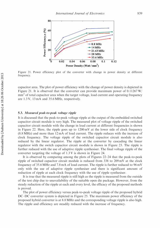
capacitor area. The plot of power efficiency with the change of power density is depicted inFigure 21. It is observed that the converter can provide maximum power of 0.11267W/mm2 of total capacitor area when the target voltage, load current and operating frequencyare 1.3V, 13mA and 35.6MHz, respectively.
5.3. Measured peak-to-peak voltage ripple
It is discussed that the peak-to-peak voltage ripple at the output of the embedded switchedcapacitor circuit module is very high. The measured plot of voltage ripple of the switchedcapacitor circuit module with the change in load current at different frequencies is shownin Figure 22. Here, the ripple goes up to 1200mV at the lower side of clock frequency(8.8MHz) and more than 12mA of load current. The ripple reduces with the increase ofclock frequency. The voltage ripple of the switched capacitor circuit module is alsoreduced by the linear regulator. The ripple at the converter by cascading the linearregulator with the switch capacitor circuit module is shown in Figure 23. The ripple isfurther reduced with the use of adaptive ripple synthesiser. The final voltage ripple of theconverter targeting the voltage of 1.3V is shown in Figure 24.
It is observed by comparing among the plots of Figures 22–24 that the peak-to-peakripple of switched capacitor circuit module is reduced from 338 to 209mV at the clockfrequency of 35.6MHz and 7.8mA of load current. The ripple is further reduced to 96mVonly with the use of adaptive ripple synthesiser and there is significant amount ofreduction of ripple at each clock frequency with the use of ripple synthesiser.
It is true that the measured ripple is still high as the ripple is measured from the outsideof the test chip due to unavailability of the suitable open die package. However, from thesteady reduction of the ripple at each and every level, the efficacy of the proposed methodsis proved.
The plot of power efficiency versus peak-to-peak voltage ripple of the proposed hybridDC–DC converter system is depicted in Figure 25. The maximum power efficiency of theproposed hybrid converter is at 8.8MHz and the corresponding voltage ripple is also high.The ripple and efficiency are steadily reduced with the increase of frequency.
Figure 21. Power efficiency plot of the converter with change in power density at differentfrequency.
International Journal of Electronics 839
Dow
nloa
ded
by [
Aub
urn
Uni
vers
ity]
at 1
8:26
06
Oct
ober
201
3
5.4. Measured DC line regulation
Figure 26 shows the measured DC line regulation of the converter for 1.3V at 13mAcurrent for a supply voltage varying from 3 to 3.6V. For input voltages more than 3.25V,good line regulation is observed. For input voltage less than 3.25V, due to the equivalent
Figure 22. Plot of voltage ripple of the switched capacitor circuit module with respect to the changein load current.
Figure 23. Plot of the voltage ripple at the converter output with respect to the change in loadcurrent when switched capacitor module is cascaded with linear regulator.
840 K. Bhattacharyya and P. Mandal
Dow
nloa
ded
by [
Aub
urn
Uni
vers
ity]
at 1
8:26
06
Oct
ober
201
3
series resistance of the flying capacitor, the voltage drop across the pass device and thedrop across the switching transistors the voltage is no more 1.3V. As expected, the voltagedrops with the input voltage after 3.25V. It is to be noted that, for load currents less than13mA, the line regulation range will be more.
Figure 24. Plot of voltage ripple at the converter output with respect to the change in load currentby cascading the linear regulator with the switched capacitor circuit module and with the use ofadaptive ripple synthesiser.
Figure 25. Plot of power efficiency with respect to the change in peak-to-peak voltage ripple of thehybrid converter.
International Journal of Electronics 841
Dow
nloa
ded
by [
Aub
urn
Uni
vers
ity]
at 1
8:26
06
Oct
ober
201
3
5.5. Measured load regulation
Figure 27 illustrates the load regulation of the regulated hybrid converter for voltage levelof 1.30V within the load current range of 1.6 to 8.2mA. Here, the switching frequency ofthe internal clock generator is 35.6MHz. The voltage is observed by changing the
Figure 27. Measured plot of regulated voltage with respect to the change in load resistance of thehybrid converter: the regulated voltage of the converter (top) and the periodic control signal(bottom) to change the load resistance.
Figure 26. Measured plot of regulated voltage with respect to the change in supply voltage of thehybrid converter.
842 K. Bhattacharyya and P. Mandal
Dow
nloa
ded
by [
Aub
urn
Uni
vers
ity]
at 1
8:26
06
Oct
ober
201
3
load resistors. The load resistance is changed by the application of a periodic control signalapplied from a function generator. The regulated voltage (top) and the control signal tochange the load resistor (bottom) are shown in Figure 27. When the control is at logic highlevel (Vdd), at that time, the load resistance is coming in parallel and the load current ofthe converter is increased (i.e. 8.2mA) otherwise the current is minimum (i.e. 1.6mA).The measured overshoot and undershoot are 282 and 355mV during switching transitionand the settling time is around 200 ns.
6. Performance comparison of simulation and measured results
The simulation of the proposed converter system is carried out to compare measuredperformance and simulated performance. It is expected that the simulated performance isthe better one but the trend of measured results are also matching with the trend ofsimulation results. Here, the plot on power efficiency and peak-to-peak voltage ripple withrespect to the change in load current of converter are depicted in Figures 28 and 29,respectively.
A noteworthy point is that the power efficiency of the measured plot in Figure 28 ishigher than the power efficiency of the simulated plot at 8.8MHz of clock frequency.It may be because of the internal load resistance with a specified value having changed dueto process variation. The trend of the rest of the measured data is consistent with itscorresponding simulation plots. The peak-to-peak average ripple of the measured plot inFigure 29 is also matching with the trend of voltage ripple achieved from the simulation.It is clear from the figure that in both simulation and the measured data, the ripple is highat the lower frequency but it is in lower side in higher frequency.
The supporting measured voltage profiles are given in Figures 30–32. Figure 30 showsthe measured ripples for 8.8MHz switching frequency and with a load current of 2.6mA.The ripple is reduced from 460 to 132mV by the use of the ripple reduction technique.Figures 31 and 32 show the ripples for 35.6MHz switching frequency and with loadcurrents of 7.8 and 13mA, respectively. Corresponding ripple reductions are from 338 to
Figure 28. Simulation and measured plot of power efficiency with respect to the change in loadcurrent of the hybrid converter.
International Journal of Electronics 843
Dow
nloa
ded
by [
Aub
urn
Uni
vers
ity]
at 1
8:26
06
Oct
ober
201
3
Figure 30. Measured plot on the steady state behaviour of the voltages at switched capacitor circuitmodule (bottom) and hybrid converter system (top) for 2.6mA of load current at 8.8MHz of clockfrequency.
Figure 29. Simulation and measured plot of peak-to-peak voltage ripple with respect to the changein load current of the hybrid converter.
844 K. Bhattacharyya and P. Mandal
Dow
nloa
ded
by [
Aub
urn
Uni
vers
ity]
at 1
8:26
06
Oct
ober
201
3
96mV and from 310 to 146mV. It may be noted that compared to simulated ripple valuesthe measured ripples are on the higher side due to board and pin parasitic. However, thetrend of ripple reduction in the simulation and that in the measurement remain similar andproves the utility of the proposed ripple reduction technique.
7. Performance comparison
As mentioned that there exists a literature (Patounakis et al. 2004) which is similar to theproposed hybrid DC–DC converter. A detailed performance comparison is done withrespect to that literature. The architecture reported in Patounakis et al. (2004) is alsoimplemented in the same 0.18mm n-well CMOS technology and the same amount ofcapacitor is used for the reported architecture and our proposed topology. The measuredcomparison is summarised in Table 1. It is transparent from this table that the DC–DCconverter system of Patounakis et al. (2004) designed in 0.18 mm CMOS technology withthe same criteria has higher ripple than that of the proposed DC–DC converter system inthis article. Here, the ripple reduction is done at the cost of maximum 0.950% reduction ofpower efficiency. Moreover, a detailed comparison is done with the existing article
Figure 31. Measured plots on the steady state behaviour of the voltages at switched capacitor circuitmodule (bottom) and hybrid converter system (top) for 7.8mA of load current at 35.6MHz of clockfrequency.
International Journal of Electronics 845
Dow
nloa
ded
by [
Aub
urn
Uni
vers
ity]
at 1
8:26
06
Oct
ober
201
3
(Patounakis et al. 2004) based on the reported performance. The comparative study of themeasured performance is presented in Table 2.
From the comparative study, it is seen that the measured power efficiency of theproposed converter is 5.55% higher than the existing literature. Although Patounakis et al.
Figure 32. Measured plots on the steady state behaviour of the voltages at switched capacitor circuitmodule (bottom) and hybrid converter system (top) for 13mA of load current at 35.6MHz of clockfrequency.
Table 1. Performance comparison of the measured results in the same technology.
Performance parameter Patounakis et al. (2004) This study
(2004) did not report the measured peak-to-peak voltage ripple of the converter system,the measured ripple of the proposed converter system is still lower than their reportedtheoretical value which is one of the major objectives of the proposed design. The value ofthe technology-independent parameter, maximum power density, is achieved by maxi-mum load power by the total capacitor area. Here, it is also observed that the powerdensity of the proposed DC–DC converter system is 0.06W/mm2 more than the reportedliterature.
8. Conclusion
In this article, an integrated hybrid DC–DC converter suitable for high dropout embeddedregulation is proposed. In the hybrid converter topology, along with a linear regulator twoswitched capacitors are used to store and recycle charge for better power efficiency.
A detailed description of the transistor-level design and major blocks which arerequired to implement the proposed converter is elaborated. Moreover, the physical designof the proposed embedded hybrid DC–DC converter system is presented. It also coverselaborate information and analysis of the measured results of the implemented embeddedhybrid DC–DC converter. The detailed measurement results are depicted to validate theidea in silicon.
The proposed converter circuit has been designed, implemented and tested in a 0.18mmCMOS process for 3.3–1.3V conversion. With two switching capacitors of 210 pF each,for more than 12mA load current and 100 pF load capacitor, measured peak-to-peakoutput voltage ripple and maximum power efficiency are 146mV and 64.97%, respec-tively. The performance comparison with the existing literature justifies the necessity of theproposed converter in embedded energy-conscious applications.
Table 2. Performance comparison of the measured results in different technology.
Performance parameter Patounakis et al. (2004) This study
Maximum clock frequency (MHz) 550 (Theoretical)ADC samplingrate: 40 (measured)
35.6
Input voltage (V) 2.5 3.3Output voltage (V) 0.65–2.5 1.26–1.36Total flying capacitor (pF) 2� 50¼ 100 2� 210¼ 420Load capacitor (pF) 100 100Maximum load current (mA) 11 13Peak-to-peak output voltage ripple (mV) 200mV (theoretical)
(measured valueis not reported)
146
Maximum power efficiency (%) 38 at 1.3V convertersystem output
43.55 at 1.3Vconverter system output
Total area (mm2) 0.42 2.72Total capacitor area (mm2) 0.32 0.15Maximum power density at 1.3Vconverter system output (W/mm2)
0.05 0.11
CMOS technology (mm) 0.25 0.18
International Journal of Electronics 847
Dow
nloa
ded
by [
Aub
urn
Uni
vers
ity]
at 1
8:26
06
Oct
ober
201
3
Acknowledgement
The authors thankfully acknowledge National Semiconductor (NSC), USA for providingFabrication support.
References
Banba, H., Shiga, H., Umezawa, A., Miyaba, T., Tanzawa, T., Atsumi, S., and Sakui, K. (1999), ‘ACMOS Bandgap Reference Circuit with Sub-1-V Operation’, IEEE Journal of Solid-State
Circuits, 34, 670–674.Bhattacharyya, K. (2011), ‘Design and Implementation of Switched Capacitor based Embedded DC-
DC Buck Converter’, Ph.D. dissertation, E&ECE Department, Indian Institute of Technology-Kharagpur.
Bhattacharyya, K., and Mandal, P. (2008), ‘A Low Voltage, Low Ripple, on Chip, Dual Switch-
Capacitor based Hybrid DC-DC Converter’, in Proceedings of the 21st International Conferenceon VLSI Design (VLSI Design 2008), Hyderabad, India, 4–8 January, pp. 661–666.
Hastings, A. (2001), The Art of Analog Layout, Englewood Cliffs, NJ: Prentice-Hall.Hazucha, P., Schrom, G., Jaehong Hahn, Bloechel, B.A., Hack, P., Dermer, G.E., Narendra, S.,
Gardner, D., Karnik, T., De, V., and Borkar, S. (2005), ‘A 233-MHz 80%-87% Efficient Four-Phase DC-DC Converter Utilizing Air-Core Inductors on Package’, IEEE Journal of Solid-
State Circuits, 40, 838–845.Lee, H., and Mok, P.K.T. (2005), ‘Switching Noise and Shoot-through Current Reduction
Techniques for Switched-Capacitor Voltage Doubler’, IEEE Journal of Solid-State Circuits, 40,
1136–1146.Lee, H., and Mok, P.K.T. (2007), ‘An SC Voltage Doubler with Pseudo-continuous Output
Regulation using a Three-stage Switchable Opamp’, IEEE Journal of Solid-State Circuits, 42,1216–1229.
Makowski, M.S., and Maksimovic, D. (1995), ‘Performance Limits of Switched-Capacitor DC-DCConverters’, in Proceedings of the 26th Annual IEEE Power Electronics Specialists Conference,
Atlanta, GA, Vol. 2, pp. 1215–1221.Milliken, R.J., Silva-Martinez, J., and Sanchez-Sinencio, E. (2007), ‘Full on Chip CMOS Low
Dropout Voltage Regulator’, IEEE Transactions on Circuits and Systems I: Regular Papers, 54,
LLP, 9.00� 9.00� 0.80mm body size’, www.national.com.Patounakis, G., Li, Y.W., and Shepard, K.L. (2004), ‘A Fully Integrated On-chip DC-DC
Conversion and Power Management System’, IEEE Journal of Solid-State Circuits, 39, 443–451.Ramadass, Y.K. (2009), ‘Energy Processing Circuits for Low-Power Applications’, Ph.D.
dissertation, Department of Electrical Engineering and Computer Science, Massachusetts
Institute of Technology, USA, pp. 3–90.Ramadass, Y.K., and Chandrakasan, A.P. (2007), ‘Voltage Scalable Switched Capacitor DC-DC
Converter for Ultra-low Power On-chip Applications’, in Proceedings of the IEEE 2007 PowerElectronics Specialists Conference, Orlando, FL, USA, 17–21 June, pp. 2353–2359.
Razavi, B. (2002), Design of Analog CMOS Integrated Circuits, New Delhi, India: Tata McGraw-
Hill Edition.Rincon-Mora, G.A., and Allen, P.E. (1998), ‘A Low-Voltage, Low Quiescent Current, Low Drop-
Out regulator’, IEEE Journal of Solid-State Circuits, 33, 36–44.Ryan, J.G., Carroll, K.J., and Pless, B.D. (1989), ‘A Four Chip Implantable Defibrillator/
Pacemaker Chipset’, in Proceedings of the Custom Integrated Circuits Conference, San Diego,CA, USA, 15–18 May, pp. 7.6/1–7.6/4.
Seeman, M.D. (2009), ‘A Design Methodology for Switched-Capacitor DC-DC Converters’, Ph.D.
dissertation, EECS Department, University of California, Berkeley, USA, pp. 158–160.
848 K. Bhattacharyya and P. Mandal
Dow
nloa
ded
by [
Aub
urn
Uni
vers
ity]
at 1
8:26
06
Oct
ober
201
3
Somasundaram, M.N., and Ma, D. (2006), ‘Low Ripple CMOS Switched-Capacitor PowerConverter with Closed-loop Interleaving Regulation’, in Proceedings of the IEEE 2006 CustomIntegrated Circuits Conference (CICC), San Jose, CA, 10–13 September, pp. 245–248.
Usami, K., and Horowitz, M. (1995), ‘Clustered Voltage Scaling Technique for Low Power Design’,
in Proceedings of the International Workshop on Low Power Design, 23–26 April, Dana Point,CA, pp. 3–8.