Design and Implementation of the Precision Personnel Locator Digital Transmitter System A Thesis submitted to the Faculty of the WORCESTER POLYTECHNIC INSTITUTE Worcester, Massachusetts, USA in partial fulfillment of the requirements of the Degree of Master of Science in Electrical and Computer Engineering by ___________________________________ Hauke C. Dämpfling December 2006 Approved: ___________________________________ Prof. R. James Duckworth, Major Advisor ___________________________________ Prof. David Cyganski, Committee Member ___________________________________ Prof. John A. Orr, Committee Member
Transcript
Design and Implementation of the Precision Personnel Locator Digital Transmitter System
A Thesis
submitted to the Faculty
of the
WORCESTER POLYTECHNIC INSTITUTE
Worcester, Massachusetts, USA
in partial fulfillment of the requirements of the
Degree of Master of Science
in
Electrical and Computer Engineering
by
___________________________________
Hauke C. Dämpfling
December 2006
Approved: ___________________________________ Prof. R. James Duckworth, Major Advisor ___________________________________ Prof. David Cyganski, Committee Member ___________________________________ Prof. John A. Orr, Committee Member
Design and Implementation of the Precision Personnel Locator Digital Transmitter System
Hauke Daempfling, WPI i
Abstract The Precision Personnel Locator project is an ongoing research project funded by the
Department of Justice, the goal of which is to provide sub-meter accuracy tracking and location
of first responders inside of buildings with no pre-existing infrastructure, especially in emergency
situations. The PPL system consists of wearable, battery-powered Locator devices that transmit a
multi-carrier “ranging signal” waveform and Reference Units that receive this ranging signal and
relay the information to a Base Station for location estimation processing and display.
This thesis describes the design and implementation of a subset of the Locator devices’
functionality, including: the digital generation of the ranging signal waveform; the coordination
of the transmissions of many Locator devices using time-sharing methods to prevent overlap of
the signals; and finally, the gathering of environmental data such as temperature and movement
of the wearer and the relaying of this data back to the Base Station.
To perform these tasks, two subsystems were designed and implemented as printed circuit
boards. The first of these is the Data Channel, which is a low power, general-purpose
communications platform that is capable of controlling the transmissions of the Locator devices
with support for up to 100 Locators transmitting every second, and it can control the power of the
Locator devices by switching portions of the system off when they are not in use. It also includes
sensors to measure the ambient temperature, movement of the device, and a “distress button” that
a first responder can press to trigger a distress signal to be transmitted to the outside of the
building. The second subsystem is the Digital Waveform Generator, which consists of a Field-
Programmable Gate Array (FPGA) and Digital-to-Analog Converter (DAC) that are capable of
generating waveforms of up to 200 MHz bandwidth. The new Locator hardware can operate on
battery power for many days.
The two subsystems were successfully tested and will serve as an important step towards
the goal of developing a deployable location and tracking system.
Design and Implementation of the Precision Personnel Locator Digital Transmitter System
Hauke Daempfling, WPI ii
Acknowledgements I would like to thank my advisor, Prof. James Duckworth, for his support and guidance
throughout my time as a graduate student and my work on this project, and especially for his
contributions and help reviewing this thesis. I would also like to thank Prof. John Orr and Prof.
David Cyganski for serving as my thesis committee members.
I am grateful to the many people who have directly contributed to my work on this thesis:
Robert Boisse, Jeffrey Cho, Jack Coyne, Gerry Harringon, Thomas Lui, Candemir Orsan, and
Hemish Parikh all assisted me greatly during the design and evaluation process.
I would like to thank the rest of the Precision Personnel Locator team for their support of
the overall project and their input to my work: Prof. Sergey Makarov, Prof. William Michalson,
Vincent Amendolare, Jason Farmer, David Holl, Jason Huang, Shashank Kulkarni and Benjamin
Woodacre have all greatly contributed to the success of the PPL project.
Finally, I would like to thank the National Institute of Justice at the Department of
Justice, who funded this research project.
Hauke Daempfling
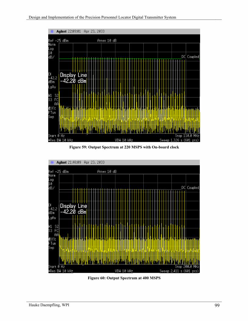
December 2006
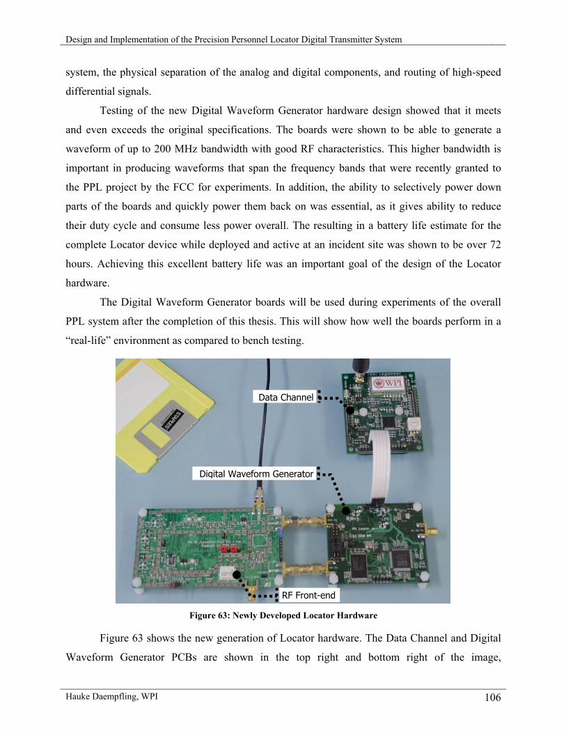
Design and Implementation of the Precision Personnel Locator Digital Transmitter System
Hauke Daempfling, WPI iii
Table of Contents Abstract .............................................................................................................................................i Acknowledgements ..........................................................................................................................ii List of Figures ..................................................................................................................................v List of Tables...................................................................................................................................vi Chapter 1. Introduction ....................................................................................................................1 Chapter 2. Background.....................................................................................................................6
2.1. Overall System Requirements...............................................................................................6 2.1.1. Meeting with Worcester Firefighters .............................................................................8 2.1.2. PPL Workshops..............................................................................................................9
Chapter 3. Data Channel and Communication Protocol ................................................................18 3.1. Multi-Transmitter Support ..................................................................................................18 3.2. Time-Division Multiplexing ...............................................................................................20 3.3. Free-Running Transmitter Calculations ..............................................................................23 3.4. Random Transmissions .......................................................................................................27
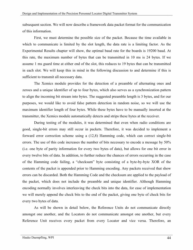
3.8.1. Data Format..................................................................................................................43 3.8.2. Communications Concept ............................................................................................46
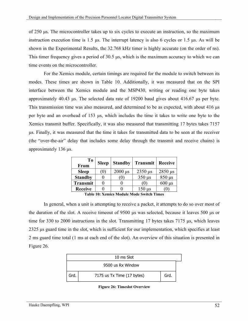
3.9. Protocol Implementation .....................................................................................................48 3.9.1. Synchronization and Timing ........................................................................................51
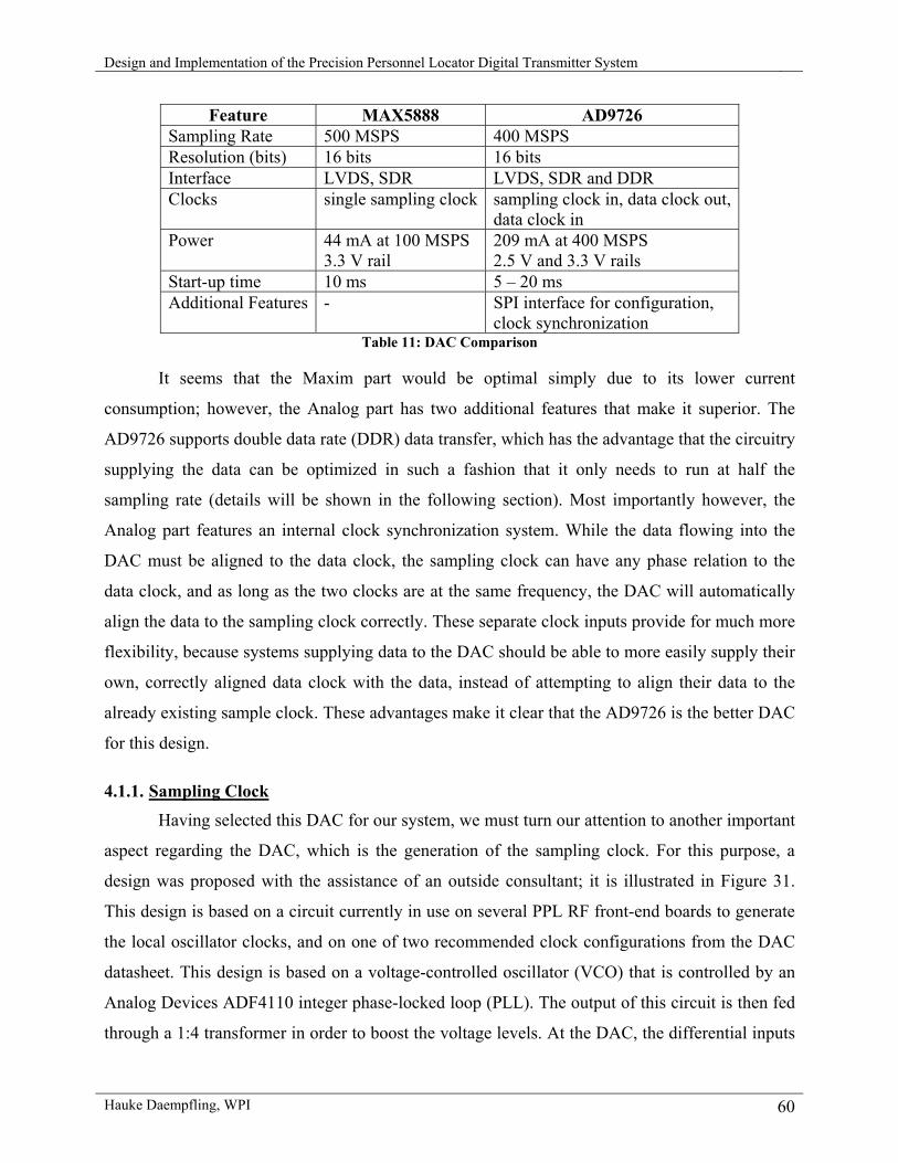
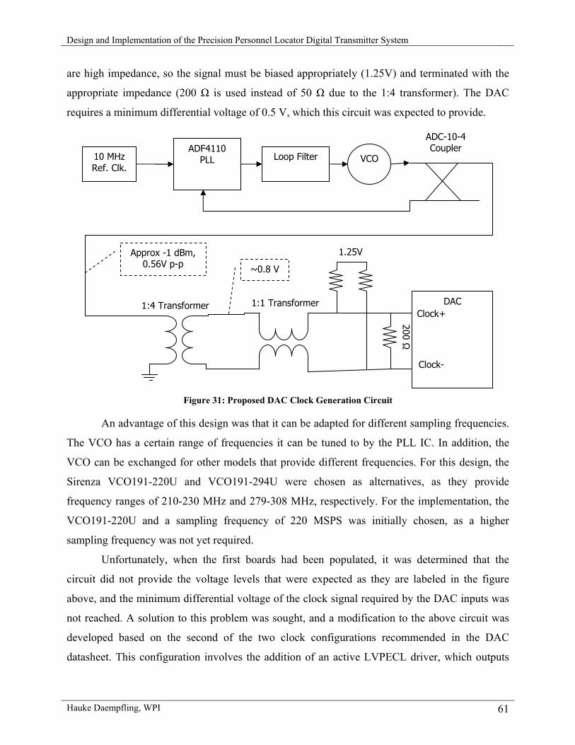
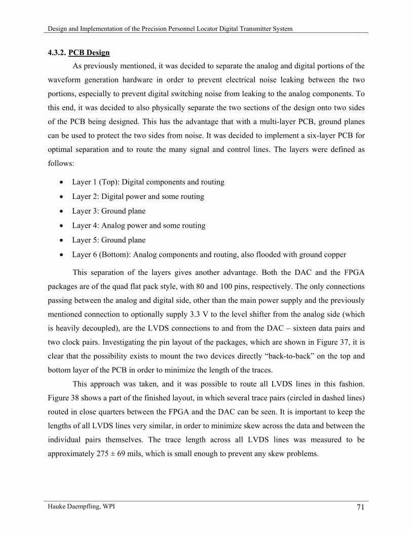
Chapter 4. Digital Waveform Generation ......................................................................................57 4.1. Digital-to-Analog Converter Design...................................................................................58
4.1.1. Sampling Clock ............................................................................................................60 4.2. Data Supplying System Design...........................................................................................62
4.2.1. High Speed Memory and CPLD ..................................................................................63 4.2.2. Field Programmable Gate Array ..................................................................................63 4.2.3. FPGA Configuration ....................................................................................................65 4.2.4. Package Selection.........................................................................................................66
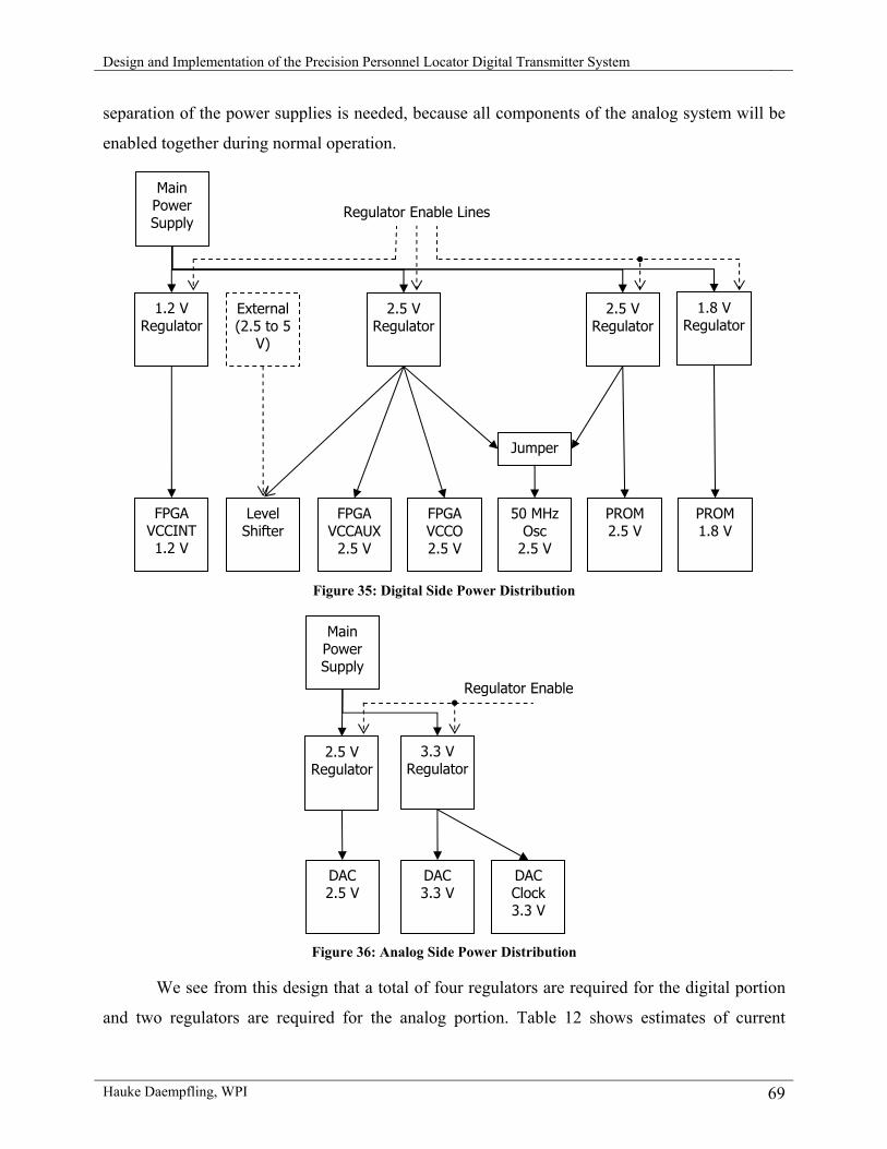
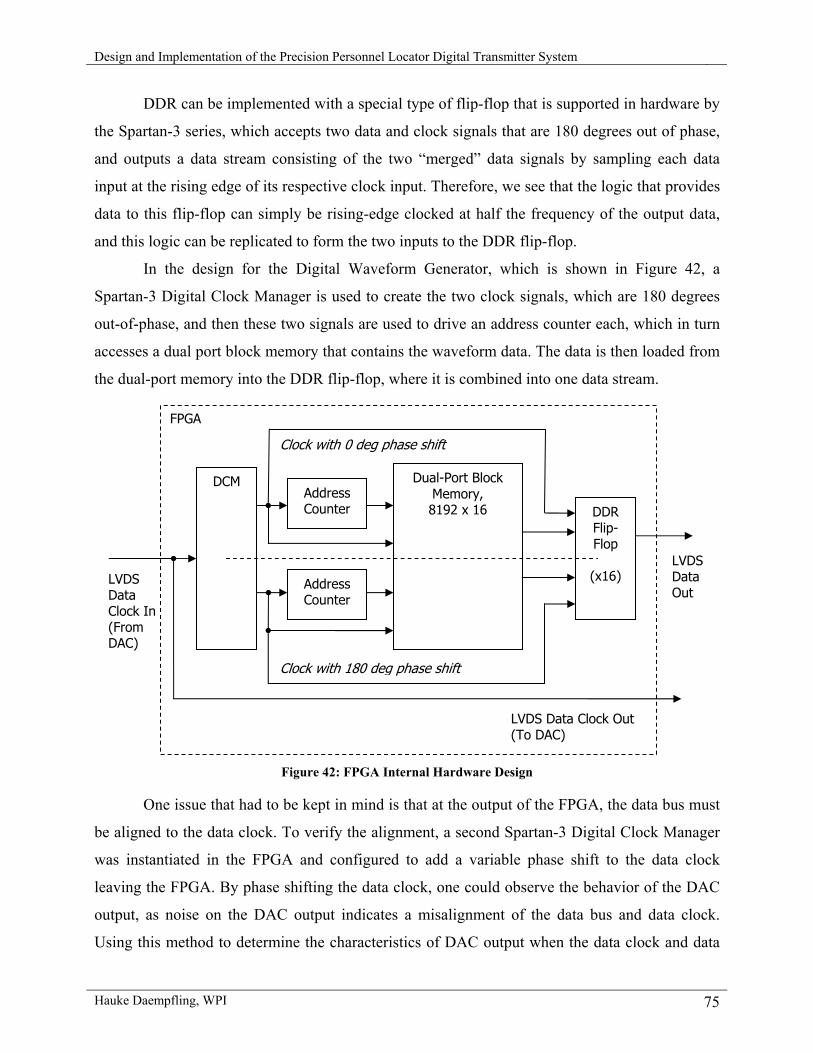
4.3. Hardware Implementation...................................................................................................67 4.3.1. Power Supply Design ...................................................................................................68 4.3.2. PCB Design ..................................................................................................................71 4.3.3. FPGA Digital Design ...................................................................................................74
Chapter 5. Experimental Results ....................................................................................................77 5.1. Data Channel .......................................................................................................................77
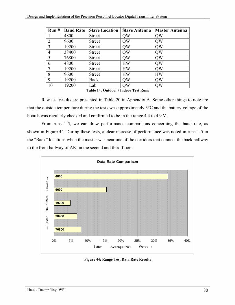
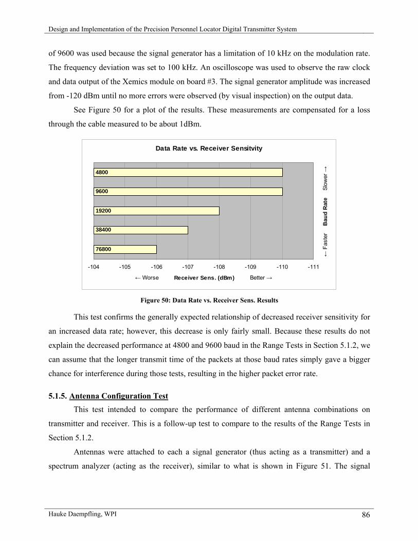
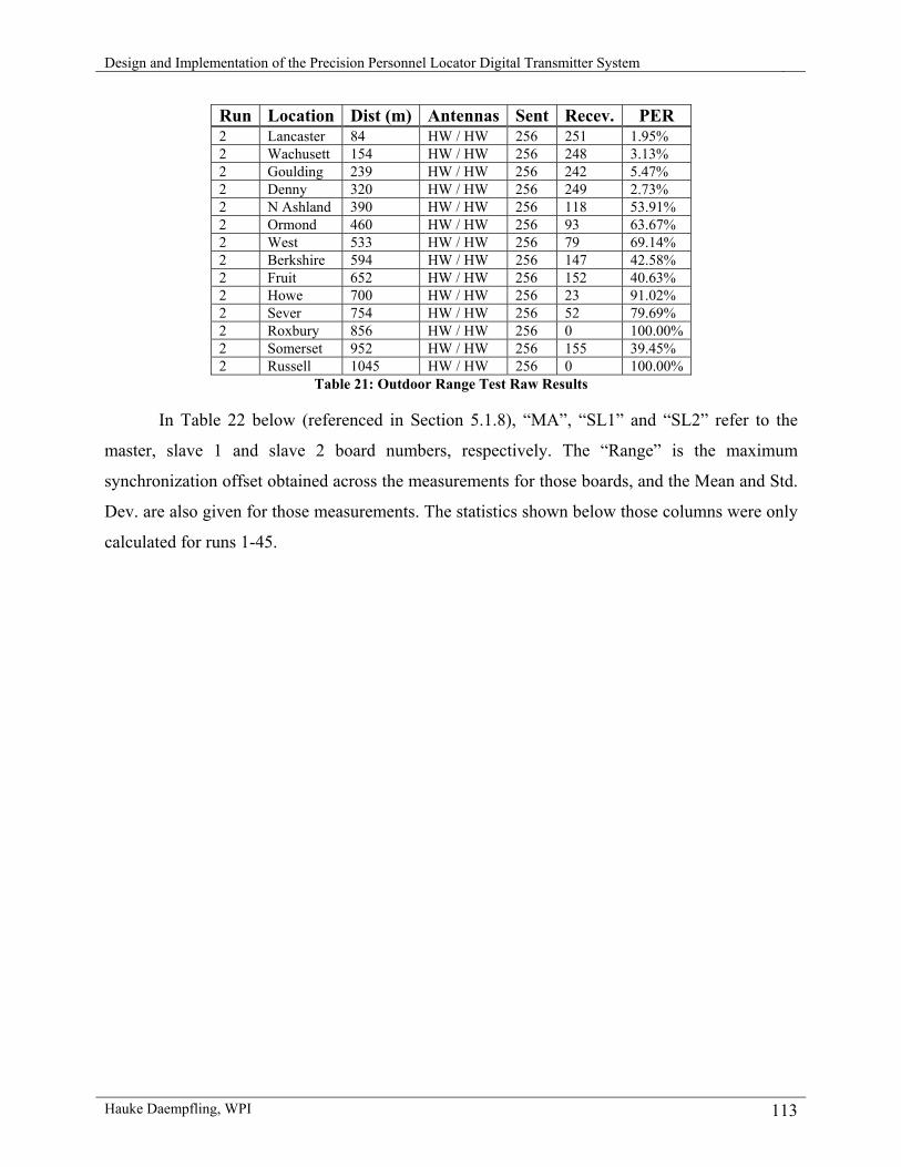
5.1.1. Hardware Performance.................................................................................................77 5.1.2. Outdoor / Indoor Range Tests ......................................................................................78 5.1.3. Outdoor Range Test .....................................................................................................84 5.1.4. Data Rate vs. Receiver Sensitivity Test .......................................................................85
Design and Implementation of the Precision Personnel Locator Digital Transmitter System
Hauke Daempfling, WPI iv
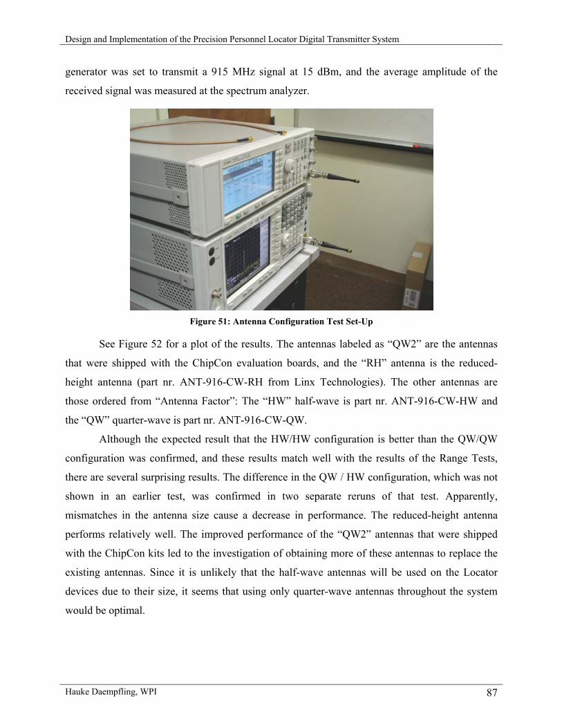
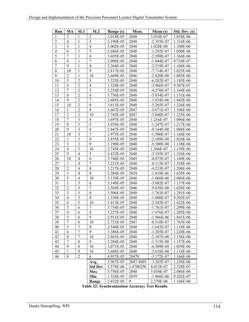
5.1.5. Antenna Configuration Test .........................................................................................86 5.1.6. Timer Accuracy Test ....................................................................................................88 5.1.7. Timer Drift Test ...........................................................................................................89 5.1.8. Synchronization Accuracy Test ...................................................................................90 5.1.9. Time Division Multiplexing Protocol ..........................................................................91
5.2. Digital Waveform Generator...............................................................................................94 5.2.1. RF Characterization......................................................................................................94 5.2.2. Power Analysis...........................................................................................................100
Chapter 6. Conclusion and Future Work......................................................................................104 6.1. Future Work ......................................................................................................................107
Chapter 7. References ..................................................................................................................108 Appendix A. Detailed Data Channel Experimental Results ........................................................111
Design and Implementation of the Precision Personnel Locator Digital Transmitter System
Hauke Daempfling, WPI v
List of Figures Figure 1: PPL System Concept ........................................................................................................2 Figure 2: Locator Unit Concept Drawings.......................................................................................3 Figure 3: Locator Overview .............................................................................................................4 Figure 4: PPL System Overview......................................................................................................7 Figure 5: Audio Proof-of-Concept System ....................................................................................10 Figure 6: RF Proof-of-Concept Receiver .......................................................................................11 Figure 7: Current Transmitter Hardware........................................................................................13 Figure 8: Multi-Carrier Signal........................................................................................................14 Figure 9: Previous Digital Waveform Generation Hardware.........................................................14 Figure 10: Overview of Locator Hardware Design........................................................................16 Figure 11: Data Channel as Part of Overall Locator Design..........................................................18 Figure 12: Time-Division Multiplexing.........................................................................................19 Figure 13: Frequency-Domain Multiplexing, Bands (left) vs. Interleaving (right) .......................19 Figure 14: TDM Overview.............................................................................................................23 Figure 15: Clock Drift ....................................................................................................................24 Figure 16: Sample Failure Times ...................................................................................................26 Figure 17: Random Transmission Scheme.....................................................................................28 Figure 18: General Locator Block Diagram...................................................................................35 Figure 19: Data Channel Hardware Block Diagram ......................................................................38 Figure 20: Completed Data Channel Hardware .............................................................................39 Figure 21: Data Channel Movement Detection Circuit .................................................................41 Figure 22: System Overview..........................................................................................................42 Figure 23: Packet Format ...............................................................................................................46 Figure 24: Protocol Overview........................................................................................................47 Figure 25: Basic Protocol Overview ..............................................................................................50 Figure 26: Timeslot Overview .......................................................................................................52 Figure 27: Synchronization ............................................................................................................54 Figure 28: Data Transmission ........................................................................................................55 Figure 29: Digital Waveform Generator as Part of Overall Locator Design .................................57 Figure 30: Digital Waveform Generator Concept..........................................................................58 Figure 31: Proposed DAC Clock Generation Circuit.....................................................................61 Figure 32: Modifications to Clock Circuit .....................................................................................62 Figure 33: Xilinx Spartan-3 Configuration Times (Source: Xilinx XAPP452).............................64 Figure 34: Digital Waveform Generator Block Diagram...............................................................68 Figure 35: Digital Side Power Distribution....................................................................................69 Figure 36: Analog Side Power Distribution...................................................................................69 Figure 37: DAC and FPGA Packages ............................................................................................72 Figure 38: Routed LVDS Data Lines.............................................................................................72 Figure 39: Completed Digital Waveform Generator Board, Top (Digital) Side ...........................73 Figure 40: Completed Digital Waveform Generator Board, Bottom (Analog) Side .....................74 Figure 41: DDR Timing Diagram (Source: AD9726 Data Sheet) .................................................74 Figure 42: FPGA Internal Hardware Design..................................................................................75 Figure 43: Slave “Street” (left) and “Back” (right) Location.........................................................79 Figure 44: Range Test Data Rate Results.......................................................................................80
Design and Implementation of the Precision Personnel Locator Digital Transmitter System
Hauke Daempfling, WPI vi
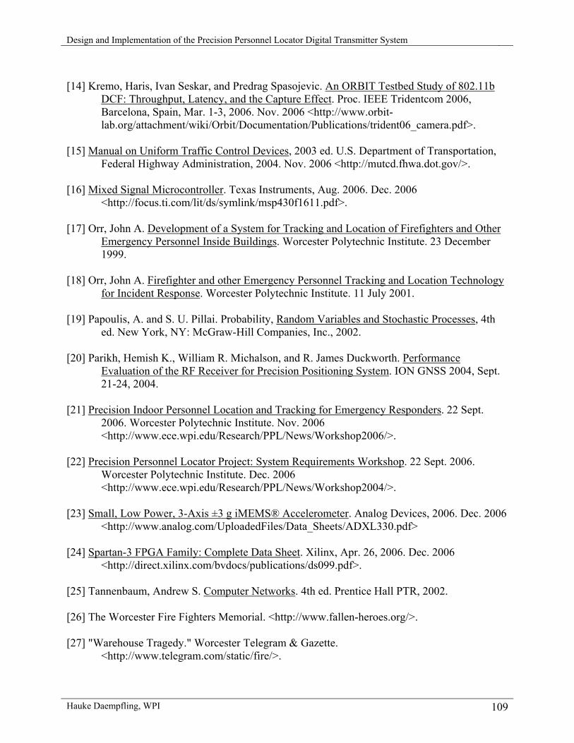
Figure 45: Range Test Distance Results ........................................................................................81 Figure 46: Range Test Antenna Results .........................................................................................82 Figure 47: Range Test Results Overview Map ..............................................................................83 Figure 48: Outdoor Range Test Locations .....................................................................................84 Figure 49: Outdoor Range Test Results .........................................................................................85 Figure 50: Data Rate vs. Receiver Sens. Results ...........................................................................86 Figure 51: Antenna Configuration Test Set-Up .............................................................................87 Figure 52: Antenna Configuration Test Results.............................................................................88 Figure 53: Actual Protocol Overview ............................................................................................92 Figure 54: Actual Synchronization ................................................................................................93 Figure 55: Actual Data Transmission.............................................................................................94 Figure 56: Multi-Carrier Test Waveform.......................................................................................95 Figure 57: Spurious Signal Comparison ........................................................................................97 Figure 58: Sampling Clock vs. Spurious Levels ............................................................................98 Figure 59: Output Spectrum at 220 MSPS with On-board clock...................................................99 Figure 60: Output Spectrum at 400 MSPS.....................................................................................99 Figure 61: Locator Power-Up Sequencing...................................................................................101 Figure 62: Power Consumption and Timing ................................................................................102 Figure 63: Newly Developed Locator Hardware .........................................................................106
List of Tables Table 1: Allotted Frequency Bands................................................................................................11 Table 2: Symbols Used ..................................................................................................................24 Table 3: Sample Failure Times (h:mm:ss) .....................................................................................27 Table 4: Required Frequency Stability for Specific Failure Times ...............................................27 Table 5: Simulation Verification Results .......................................................................................30 Table 6: Sample Probability Calculations......................................................................................31 Table 7: Transceiver Modules........................................................................................................34 Table 8: Data from Locator to Base Station...................................................................................45 Table 9: Data from Base Station to Locator...................................................................................45 Table 10: Xemics Module Mode Switch Times.............................................................................52 Table 11: DAC Comparison...........................................................................................................60 Table 12: Current Consumption Estimates ....................................................................................70 Table 13: Regulator Selection ........................................................................................................70 Table 14: Outdoor / Indoor Test Runs ...........................................................................................80 Table 15: Timer Drift Test Results ................................................................................................89 Table 16: SNR Comparison Results...............................................................................................95 Table 17: Harmonic Distortion Test...............................................................................................96 Table 18: Signal Power Levels.......................................................................................................96 Table 19: Battery Life Calculation...............................................................................................102 Table 20: Outdoor / Indoor Range Test Raw Results ..................................................................112 Table 21: Outdoor Range Test Raw Results ................................................................................113 Table 22: Synchronization Accuracy Test Results ......................................................................114
Design and Implementation of the Precision Personnel Locator Digital Transmitter System
Hauke Daempfling, WPI 1
Chapter 1. Introduction On December 3, 1999, six firefighters were killed in a disastrous fire at the Worcester
Cold Storage and Warehouse in Worcester, Massachusetts [3, 26, 27, 30]. Most, if not all, of
these deaths could possibly have been prevented if the firefighters had had some better way to
navigate inside the building despite the thick smoke and complicated layout of the corridors. This
event led to the authoring of a whitepaper by Prof. John Orr [17] outlining the basic requirements
for a system to locate and track first responders inside of buildings, and the subsequent launch of
the Precision Personnel Locator research project, or PPL, which has been funded with a total of
about $3 million by the US Department of Justice.
In general, precise location estimation of persons inside of buildings without preexisting
infrastructure for such purposes is a highly useful yet technically challenging problem. As will be
described in more detail later, this is due largely to the fact that radio signals reflect from metal
objects, creating multiple copies of the same signal and obscuring the direct path to the radio
transmitter. Currently, there are no commercially available systems that can accomplish precise
location and tracking. If such systems can be developed, the applications include uses for law
enforcement, correctional facilities, and emergency first responders, such as firefighters [28]. The
Precision Personnel Locator research project aims to develop technology for these applications
by building an RF-based location and tracking system.
The PPL system consists of wearable Locator devices that transmit a multi-carrier
“ranging signal” waveform that spans as much as a few hundred MHz and Reference Units that
receive this ranging signal and relay the information to a Base Station for processing and location
estimation. Figure 1 depicts this situation for the case of firefighters. The concept is that every
person to be tracked wears a Locator unit (in the figure these are referred to as “transmitter
badges”), most likely as part of their standard turnout gear. The Reference Units either are
mounted directly on the first responders’ vehicles or are deployed from them, allowing for a rapid
setup of the entire system. The incident commander has a tactical display as part of the Base
Station, most likely on their command vehicle, to view the positions of the persons being tracked.
This tactical display would have the capability to display the location of all or only a few selected
Locator units in real-time and the paths they have followed over time. Such information could in
turn be disseminated off-site or to hand-held units such as PDAs. The location and path
Design and Implementation of the Precision Personnel Locator Digital Transmitter System
Hauke Daempfling, WPI 2
information could then be used either to guide a lost user out on the path they entered the
building, or to guide a rescue team into the building and directly to the person in need of
assistance.
Figure 1: PPL System Concept
The figure above makes another important point, which is that the signal transmitted by
the Locator devices is reflected by metal objects and scatters. This effect is called multipath,
because each reflected signal that reaches the receiver is seen as a different “path” to the
transmitter. The receiver then has the difficult task of selecting the true path, which is usually the
shortest path, but not necessarily the strongest signal. Multipath effects can also cause certain
frequencies in the signal to be faded out and others to be amplified. This problem is solved by the
unique signal structure, algorithms and system architecture of the PPL system [6].
Design and Implementation of the Precision Personnel Locator Digital Transmitter System
Hauke Daempfling, WPI 3
The function of the Locator units is to transmit the “ranging signal”, consisting of many
carriers, at pre-determined time intervals, so that multiple units may time-share their
transmissions. Figure 2 shows a concept drawing of what a Locator device might look like. The
units would be hand-held, being the size of a cell phone or walkie-talkie. They feature a distress
button that can be used by a first responder to trigger a distress call to be sent to the outside of the
building in case of emergency, and a status display for information such as battery charge status.
As can be seen in the figure, there are two separate antennas – a PIFA-type antenna for the
ranging signal, and a monopole antenna for data communication. Note that the reasons for
implementing these two radio channels separately will be discussed in this thesis.
Figure 2: Locator Unit Concept Drawings
The ranging signal is generated on the Locators by a “software radio” type system.
Digital samples of the signal waveform are generated by a Field Programmable Gate Array
(FPGA) and provided to a Digital-to-Analog Converter (DAC) at a high speed – at least twice the
bandwidth of the signal, i.e. a few hundred MHz. The DAC passes the generated signal to a radio
frequency (RF) front-end, which up-converts the signal in the analog domain to the desired center
frequency. In addition, the entire Locator must be able to be switched off when it is not in use to
conserve power and in order to allow for the time-sharing of ranging signal transmissions. Figure
3 shows this system, in which the Locator has been divided into three subsystems: the digital
generation of the ranging signal waveform via the FPGA and DAC, the radio frequency front-end
that upconverts and transmits this signal, and lastly a control module that handles tasks such as
Status Display
Distress Button
Circuit Boards
Patch Antenna
Data Comm. Antenna
Design and Implementation of the Precision Personnel Locator Digital Transmitter System
Hauke Daempfling, WPI 4
powering the other two parts of the Locator on and off as necessary and communicating
commands and status data. This control module is known as the Data Channel.
Figure 3: Locator Overview
The focus of the work described in this thesis lies in the design, implementation and
testing of the digital portion of the Locator units, consisting of the power control, transmission
coordination, and digital waveform generation subsystems shown (shaded) above. Some
additional tasks of the Locator units are to monitor the status of the environment, the
physiological status of its wearer and to provide limited communication capabilities, such as a
“distress call” to the outside of the building. There are several challenges in these tasks. The
Locator units must be capable of running on battery power for several days. The waveform
generation system must be capable of supplying data to the DAC at a high speed and still have a
low power consumption, for example by enabling the circuit for only short periods of time. In
addition, the transmissions of multiple Locators must be coordinated, and the status information
and possible distress call must be communicated to the Base Station.
In order for the Locator to be modular for testing and to be able to better shield the
different systems from one another in case of problems, it was decided to implement the
subsystems shown above as three separate printed circuit boards (PCBs). The first PCB is the
“Data Channel” Power Control, Transmission Coordination, and
Environmental Status Data
Digital Waveform Generation
Radio Frequency Transmitter Front-end
Comm. Module
Micro-controller
Sensors
FPGA
DAC
LPF
Mixer
PA
BPF
LO
Clock
Design and Implementation of the Precision Personnel Locator Digital Transmitter System
Hauke Daempfling, WPI 5
Data Channel, which is intended to take over the power control, transmission control, status
monitoring, and general data communication tasks of the Locator, and the second PCB is the
Digital Waveform Generator, which is intended to replace the existing prototype waveform
generators and produce the ranging signal waveform for the RF front-end. Note that the RF front-
end is currently being developed as a third subsystem by other members of the PPL team.
The Data Channel subsystem was developed as a more general-purpose platform for two-
way wireless communications on an RF band separate from the ranging signals. It was
implemented as a small, battery powered printed circuit board (PCB). The PCB includes a low-
power microcontroller, a communications module capable of communications in the license-free
900 MHz “Industrial, Scientific and Medical” (ISM) radio band, and several peripherals such as
an accelerometer for movement detection and a temperature sensor. The hardware is capable of
operating on battery power for several days and has several interface ports to connect to other
parts of the Locator, such as for overall power control of the Locator device. Because the PCBs
operate on a wireless channel separate from the ranging signal, they could even be used as a
backup for basic communication in case the ranging signal fails, for example to communicate the
distress signal.
The Digital Waveform Generator subsystem is a redesign of an existing version of
waveform generator hardware and is intended to be used in conjunction with a new RF
transmitter front-end currently under development. It was implemented as a small PCB that
attaches directly to the new RF front-end. The boards’ major components are a Xilinx Spartan-3
FPGA and an Analog Devices DAC, accompanied by supporting circuitry such as clock
generation for the DAC. This new hardware was developed to better approximate a final product
in terms of size, power consumption, and sampling rate, as the previous generation of hardware
was larger, and the FPGA and DAC were not optimal compared to the required sampling rate,
and therefore also consumed more power.
This thesis presents the design, implementation and testing of the Data Channel and
Digital Waveform Generator subsystems. In the next chapter, the background of the PPL project
will be presented, including its history and the overall design requirements. Then, in the
following chapters, the design of each subsystem will be discussed, followed by the
implementation and testing of each.
Design and Implementation of the Precision Personnel Locator Digital Transmitter System
Hauke Daempfling, WPI 6
Chapter 2. Background In this chapter, the requirements for the different portions of the PPL system with a focus
on the Locator device will be presented, followed by a brief history of the PPL project. The
previous generation of Locator hardware is presented, followed by the design requirements for
the new Locator hardware, with a focus on the digital subsystems of the Locator.
2.1. Overall System Requirements At the beginnings of the PPL project in 1999 [17], several requirements for the system
were laid out, many of which evolved over time to meet the requirements of users and the
technical realities of implementing the system [18]. This section describes the system
requirements as they stood at the time of writing, with some mention to the origins of these
requirements. It should be noted that, in several cases, there were two sets of requirements for
two different goals: the theoretical “final production system” level requirements, and the
prototype system requirements that apply to the systems described in this thesis, which represent
a step towards the final requirements.
An overview of the PPL system is presented in Figure 4. The Locator units transmit the
ranging signal, which is received by the Reference Units, which in turn relay the data back to the
Base Station. For this reason, the Locators are often referred to simply as transmitters, and the
Reference Units as receivers. The Locator units are worn by the first responders entering the
building or structure, and the units collect environmental and psychological status information
and transmit it outside the building, in addition to transmitting the ranging signal. The Reference
Units could be mounted on a first responder vehicle (such as a fire truck), or they could be
deployed from the vehicles as mobile reference units. The Base Station could be mounted on, for
example, the vehicle of the incident commander. It is obvious that the Locator units must be
completely free to operate on their own, with “no wires attached” and powered by a battery.
It should be noted that many of the discussions of the PPL project are in the context of
firefighters, but the system is actually very general-purpose. Market studies and focus groups
were conducted [28] that showed that there is interest in this kind of technology from groups such
as law enforcement and correctional facilities as well. In some cases, the requirements differ, but
the basic work being done on the PPL systems and algorithms can be adapted to meet these
different needs.
Design and Implementation of the Precision Personnel Locator Digital Transmitter System
Hauke Daempfling, WPI 7
Figure 4: PPL System Overview
The most obvious requirements for the system are accuracy and reliability. The system
must be able to provide real-time location information in three dimensions for each separate user
of the system. The accuracy of the position should be good enough to let the users know which
side of a wall a person is on, to be able to direct a search and rescue team to the correct room, so
the positioning requirement calls for ±1 foot accuracy. The system must support up to 100 users
simultaneously, allowing for use in large-scale emergencies where this number of first responders
is likely.
The operating rage of the system was originally specified to be at least 2000 ft (about 610
m), so that it would be able to cover an entire city block. However, in order to stay within FCC
regulations and because such a range is not yet required for testing, the prototype system
specifications stated that a range of 100 m is enough. This range covers the Atwater-Kent
Locator Unit
Building or Structure
Reference Unit
Reference Unit
Reference Unit
Base Station
Locator Unit
Locator Unit
Ranging Signal & Status Data
Control Commands
Relayed Data
Design and Implementation of the Precision Personnel Locator Digital Transmitter System
Hauke Daempfling, WPI 8
building at WPI, which is often used for testing, and is representative of other large, commercial
buildings. In addition, it can be assumed that the existing transmitters would need to only be
modified for a higher transmission power to achieve a greater range.
The system should track the path users have taken over time by periodically recording
their location. In order to acquire this tracking information, and in order to provide real-time
location information to the users, the system must update the position of each Locator device at
least once a second. The path information that is gathered could be displayed on the Base Station,
and it could also be relayed to hand-held units, possibly even ones carried by the first responders
themselves. This would allow for a “self-rescue” type operation, where users who may have
become lost or disoriented could find their own way out.
Finally, the Locator devices should collect environmental and psychological information,
so that this information can be relayed to the Base Station and the status of the person inside the
building is better known. This should include a “distress signal” that a first responder can trigger
when in need of assistance in emergencies.
2.1.1. Meeting with Worcester Firefighters In October 2005, researchers from the WPI PPL project met with officials from the
Worcester Fire Department to discuss both system requirements and to get an idea of existing
firefighter equipment [29]. Several important insights into how the PPL system might integrate
into fire departments’ equipment and routines were gained. In general, one must realize that
typical fire departments may not have a great deal of funding and that most firefighters operate
without “high-tech gadgets” – the standard turnout gear includes only boots, pants, a jacket, a
helmet, a flashlight and possibly a radio. Other equipment, such as axes, is taken from the fire
truck only when needed. So-called “self contained breathing apparatuses” (SCBAs) are also part
of the equipment of a fire department, but there may not be enough for every firefighter. SCBAs
are also sometimes forgotten, or even abandoned by firefighters when they are out of air. The
SCBAs typically also include a “Personal Alert Safety System” (PASS), which is a device that
emits a loud beeping noise when it detects non-movement of the firefighter, allowing for other
firefighters to find a downed colleague.
The main theme that became apparent at this meeting was that the Locator devices must
be very simple to use, hard to lose or forget, and be robust. When arriving at the scene of an
incident, firefighters should not need to remember to pick up a Locator device (in case it is
Design and Implementation of the Precision Personnel Locator Digital Transmitter System
Hauke Daempfling, WPI 9
attached to some kind of charging station or something similar), or to turn it on. This means that
it would be preferable to be able to issue a Locator device to every firefighter so that it can be
worn at all times, or even that it is sewn into or otherwise securely attached to the firefighter’s
turnout gear, such as the jacket. This shows the need for two more requirements: The devices
must be low-cost, so that one could be issued for every firefighter in a department, and they must
be very low-power, preferably even with the ability to remotely turn off a device when it is not at
the scene of an incident. However, another important point is that if a device is so low-power that
it does not need to be recharged often, this might actually be a disadvantage, as it does not build a
habit for firefighters to regularly recharge their devices.
In respect to the possible “self-rescue” feature of the system, the point was made that
inside a burning building there is often very low or absolutely no visibility, due to thick smoke
and/or the power being cut off to the building. Therefore, it would be difficult for a firefighter to
see the screen of a device providing self-rescue information, or the device could be dropped and
easily lost. In addition, the environment can often be very noisy, making audio clues also
somewhat troublesome.
In summary, the meeting with the firefighters confirmed that the top priorities for the
Locator devices are small size, robustness, as well as low cost. In addition, the fact that every fire
is an “organized chaos” makes it clear that rapid deployment and ease-of-use are especially
important to the system as well.
2.1.2. PPL Workshops The first workshop concerning the PPL project was held in June of 2004 [22] and was
attended by representatives from government, fire departments, law enforcement offices, and
correctional facilities. At this workshop, the system requirements and priorities for the PPL
system were established; many of these requirements are reflected in the above sections.
In August 2006, a workshop entitled “Precision Indoor Personnel Location and Tracking
for Emergency Responders” was held at WPI [21]. At this workshop, representatives from
industry and research gathered to present their different approaches to the issue of indoor location
and tracking, and discussed common requirements for such systems. Through working group
sessions, several conclusions for requirements were reached [31]. Many of these conclusions
simply confirm the need for reliability, accuracy, etc. and underline the different requirements for
different end users. However, one point differs from the previous discussion here, which is that
Design and Implementation of the Precision Personnel Locator Digital Transmitter System
Hauke Daempfling, WPI 10
self-rescue could actually be a very important feature. This is because a firefighter is not always
in a zero-visibility environment, and may easily be in a situation where he or she must escape
from a building or structure, without the time for a rescue team to enter the building. So, although
for the design of the Locator devices, self-rescue was not deemed a required functionality, this
feature should not be eliminated from the list of general, future system requirements.
To summarize all these requirements for the focus of this thesis, which is on the Locator
devices, it is clear that the Locators must be small and low-power, able to reliably transmit the
ranging signal, and to communicate status information back to the Base Station.
2.2. PPL Project History The PPL project has benefited much from the work being done at WPI in the areas of
radio navigation, radar sensing, and super-resolution techniques. In a paper by Professors
Cyganski, Orr, and Michalson of WPI, a novel approach to range estimation is described [6]. This
approach uses a multi-carrier signal structure and a matrix decomposition algorithm to analyze
the relative phase shifts of each carrier to determine the time difference of arrival (TDOA) which
can in turn be used to calculate the distance to the transmitter from two receivers. In addition, this
algorithm allows for the separation of the direct-path and multipath signals, and its multi-carrier
structure allows it to be robust against frequency selective fading.
This algorithm was implemented in a proof-of-concept system that used audio waves
instead of RF frequencies [13]; this allowed for rapid prototyping with standard PC hardware.
The original signal consisted of 101 carriers generated at 44100 samples per second, and the
wavelengths of the kHz-range audio signals in air correspond to the wavelengths of an RF signal
in the GHz range. This system, shown in Figure 5, showed that this approach is feasible, and thus
paved the way for the next stage of the project, which was an RF-based prototype system.
Figure 5: Audio Proof-of-Concept System
Design and Implementation of the Precision Personnel Locator Digital Transmitter System
Hauke Daempfling, WPI 11
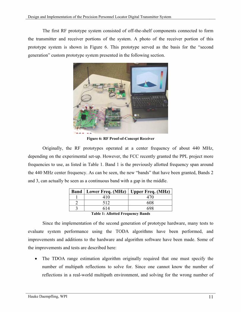
The first RF prototype system consisted of off-the-shelf components connected to form
the transmitter and receiver portions of the system. A photo of the receiver portion of this
prototype system is shown in Figure 6. This prototype served as the basis for the “second
generation” custom prototype system presented in the following section.
Figure 6: RF Proof-of-Concept Receiver
Originally, the RF prototypes operated at a center frequency of about 440 MHz,
depending on the experimental set-up. However, the FCC recently granted the PPL project more
frequencies to use, as listed in Table 1. Band 1 is the previously allotted frequency span around
the 440 MHz center frequency. As can be seen, the new “bands” that have been granted, Bands 2
and 3, can actually be seen as a continuous band with a gap in the middle.
Since the implementation of the second generation of prototype hardware, many tests to
evaluate system performance using the TODA algorithms have been performed, and
improvements and additions to the hardware and algorithm software have been made. Some of
the improvements and tests are described here:
• The TDOA range estimation algorithm originally required that one must specify the
number of multipath reflections to solve for. Since one cannot know the number of
reflections in a real-world multipath environment, and solving for the wrong number of
Design and Implementation of the Precision Personnel Locator Digital Transmitter System
Hauke Daempfling, WPI 12
signals may perturb the correct solution, an addition to the algorithm known as “auto-
Nsig” allowed for it to automatically determine the best number of signal paths to solve
for.
• The initial versions of the algorithms used only one of the sidebands of the received
signal. Algorithm improvements that allowed processing of both sidebands of the signal
meant a doubling of the bandwidth available for range estimation.
• A Windows-based GUI for data collection was developed. This had previously been done
with tedious manual editing and execution of MATLAB scripts. This GUI made the
process of collecting data during testing much more efficient, allowing more tests to be
performed.
An important point that is raised above is increasing the bandwidth. It has been shown [7,
20] that, generally speaking, increased bandwidth results in better range estimates. Therefore,
tests were performed in which the original transmitter bandwidth of 25 MHz was increased to 50
MHz and above, which allowed for better range estimation.
During the testing of the TDOA algorithm, some important benchmarks were reached, for
example, a first test was performed that showed that the TDOA algorithm could be used to
accurately locate a transmitter in two dimensions in an outdoor environment. An important
element of this test was that the transmitter did not share any clock signals with the receivers, i.e.
it was completely free-running “with no wires attached”, as a transmitter in the real world would
be.
2.3. Existing Digital Hardware Design The work described in this thesis involved improving the design of the Locator devices,
which was based on the previous generation of simple transmitter hardware described in [8].
Because this thesis focuses on the digital hardware of the Locator devices, we will describe this
portion of the previous version of hardware, a diagram of which is reproduced from [8] in Figure
7. The “Digital Controller” and “High Speed D/A” portions were completely redesigned as part
of the work on this thesis, and a redesign of the RF front-end is currently underway by other
members of the PPL team.
Design and Implementation of the Precision Personnel Locator Digital Transmitter System
Hauke Daempfling, WPI 13
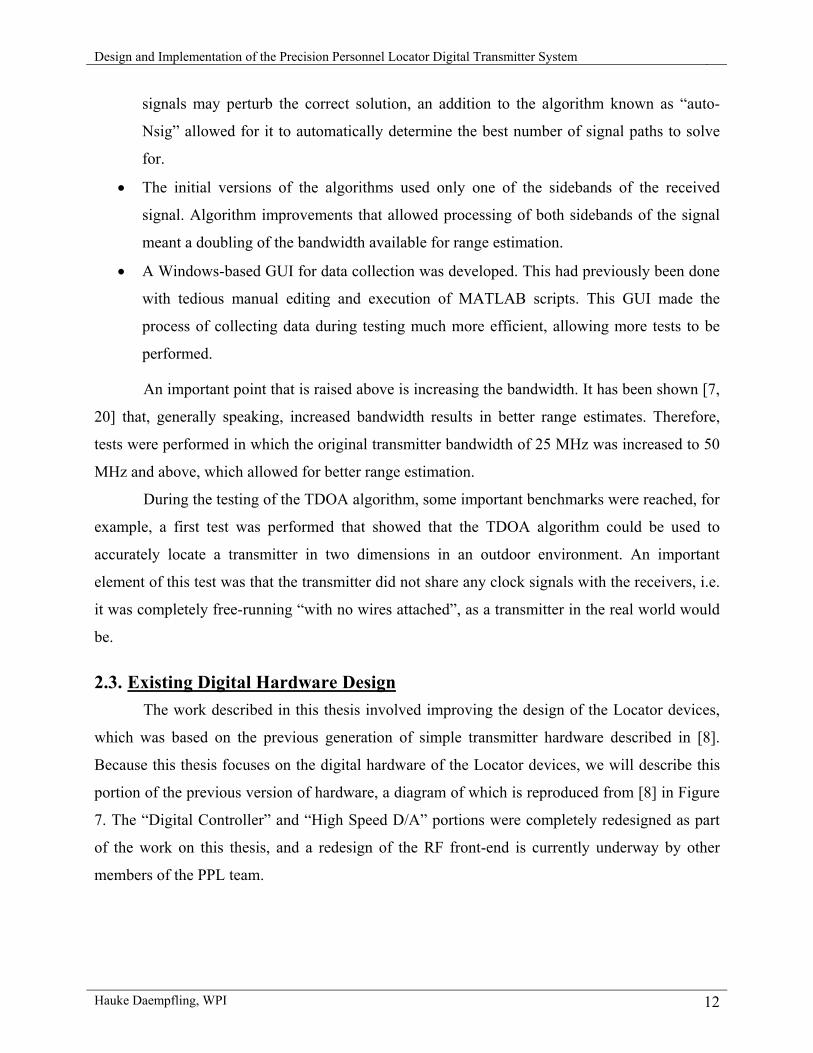
Figure 7: Current Transmitter Hardware
The digital portion of the previous transmitter prototype was responsible for generating a
100 MHz bandwidth signal that contains the multi-carrier waveform. This waveform normally is
adapted for different bandwidths in different experiments, but in general, it consists of 50 or 51
equally spaced carriers. In [8], 50 carriers are spaced 244 kHz apart, beginning at 2.44 MHz,
resulting in about 12.2 MHz total bandwidth (see Figure 8).
The transmitter hardware consists of two separate boards as shown in Figure 9, a general-
purpose digital controller board (bottom) that was also used on the receiver, and a digital-to-
analog conversion board (top). The digital controller board features a Xilinx Virtex-2 FPGA with
the required configuration PROM and power supplies. In addition, it has a 64 MB SDRAM, an
Ethernet transceiver, and an RS232 interface. A number of FPGA pins are present on pin headers
to provide for up to 16 bits of data or 14 bits of data and two clock signals using the low-voltage
differential signaling (LVDS) standard to interface to the DAC board.
The digital-to-analog conversion board contains an Analog Devices AD9736 DAC, which
is capable of sampling rates of up to 1.2 GSPS with 14 bits of resolution. The DAC receives its
sampling clock from either an external clock via an SMA connector or a clock from the digital
controller board. The DAC features an LVDS interface, and expects an input of 14 bits of data
together with an additional data clock signal from the FPGA. In addition, the DAC can optionally
provide a clock signal to the FPGA.
Design and Implementation of the Precision Personnel Locator Digital Transmitter System
Hauke Daempfling, WPI 14
Figure 8: Multi-Carrier Signal
Figure 9: Previous Digital Waveform Generation Hardware
The ranging signal generated by these boards consisted of 8192 samples, making up a
symbol, that were sampled at 200 MSPS, giving a symbol duration of 40.96 µs. The samples were
stored in the FPGA’s block memory and were provided to the DAC using double data rate (DDR)
transfer, in which data is sampled on both the rising and falling clock edge, allowing for a clock
frequency of half the data rate. The signal generated by this digital waveform generation system
High-Speed D/A
Digital Controller
Design and Implementation of the Precision Personnel Locator Digital Transmitter System
Hauke Daempfling, WPI 15
was passed along to the RF front-end, which upconverted the signal to a center frequency
depending on the experimental set-up.
The disadvantage of this previous version of hardware was that it was unnecessarily
powerful for a deployable system, because it was intended as a general-purpose platform. For
example, the digital controller board contains features such as a large SDRAM and an Ethernet
controller, which are not necessary for the final Locator device. Also, the FPGA contains much
more logic than is actually needed to generate the waveform (only 1% of its logic resources were
actually used, and only 17% of its Block RAM), and the entire design had not been tested for use
with higher bandwidths than 100 MHz. In addition, the boards are large and do not show what a
final Locator device might look like in terms of size.
Another large disadvantage was that the previous version of the hardware was not
optimized in terms of current consumption. The hardware was not designed to enable easy or fast
power control, meaning that the boards were powered either completely on or completely off. In
addition, as will be shown in a later chapter, supporting multiple Locators requires time-sharing
of the transmission of the ranging signal. This means that the Locator should be switched off
when it is not needed, both to prevent overlap of two transmitters’ signals, and to conserve
power. However, the previous design required too much time to power on and off, effectively
preventing duty cycling of the hardware and preventing support for multiple transmitters.
One should note that the previous generation of hardware was purely a transmitter for the
ranging signal and did not include any provisions for several of the features that have been
described as requirements in the previous sections, such as environmental status information, or
any other kind of data communication ability that would allow for implementation of a time-
sharing scheme. This was one of the reasons for developing a new version of the hardware, with
the requirements as set forth in the following section.
2.4. Locator Design Requirements In late 2005, the existing prototype transmitter and receiver hardware worked well and
many tests had been performed with it. However, this hardware had several shortcomings, as
described in the previous sections. Therefore, it was decided to develop the new Locator
hardware described in this thesis. This section presents the specifications for this new generation
of hardware.
Design and Implementation of the Precision Personnel Locator Digital Transmitter System
Hauke Daempfling, WPI 16
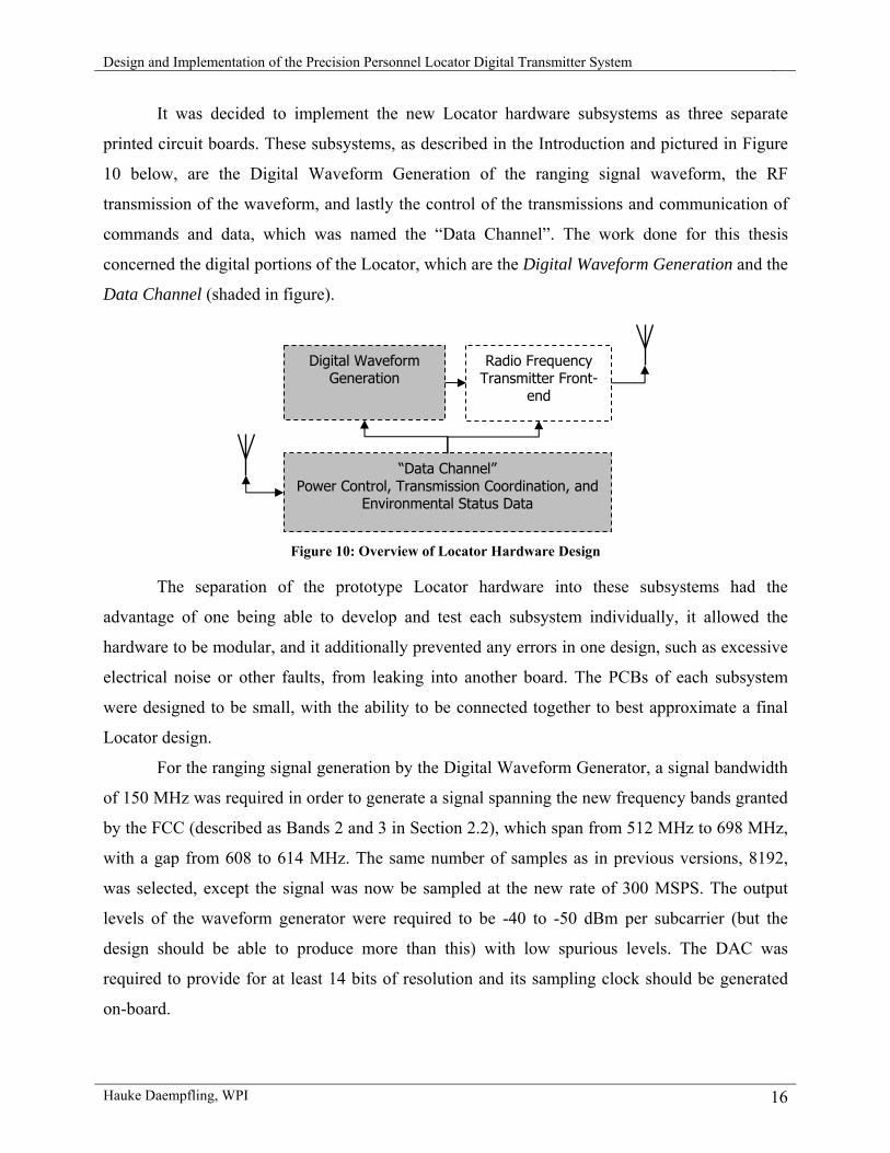
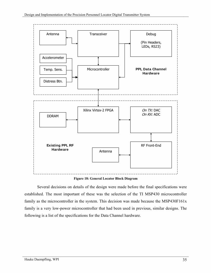
It was decided to implement the new Locator hardware subsystems as three separate
printed circuit boards. These subsystems, as described in the Introduction and pictured in Figure
10 below, are the Digital Waveform Generation of the ranging signal waveform, the RF
transmission of the waveform, and lastly the control of the transmissions and communication of
commands and data, which was named the “Data Channel”. The work done for this thesis
concerned the digital portions of the Locator, which are the Digital Waveform Generation and the
Data Channel (shaded in figure).
Figure 10: Overview of Locator Hardware Design
The separation of the prototype Locator hardware into these subsystems had the
advantage of one being able to develop and test each subsystem individually, it allowed the
hardware to be modular, and it additionally prevented any errors in one design, such as excessive
electrical noise or other faults, from leaking into another board. The PCBs of each subsystem
were designed to be small, with the ability to be connected together to best approximate a final
Locator design.
For the ranging signal generation by the Digital Waveform Generator, a signal bandwidth
of 150 MHz was required in order to generate a signal spanning the new frequency bands granted
by the FCC (described as Bands 2 and 3 in Section 2.2), which span from 512 MHz to 698 MHz,
with a gap from 608 to 614 MHz. The same number of samples as in previous versions, 8192,
was selected, except the signal was now be sampled at the new rate of 300 MSPS. The output
levels of the waveform generator were required to be -40 to -50 dBm per subcarrier (but the
design should be able to produce more than this) with low spurious levels. The DAC was
required to provide for at least 14 bits of resolution and its sampling clock should be generated
on-board.
“Data Channel” Power Control, Transmission Coordination, and
Environmental Status Data
Digital Waveform Generation
Radio Frequency Transmitter Front-
end
Design and Implementation of the Precision Personnel Locator Digital Transmitter System
Hauke Daempfling, WPI 17
The system had to support up to 100 simultaneous users, giving location updates at least
once a second. In addition, the Locators were required to be low-power, consuming as little
power as possible when running, to provide detailed power control for individual portions of the
circuits, and to have rapid turn-on times for power saving through duty cycle reduction. The
system was required be able to operate continually on battery power for at least several (on the
order of 6-12) hours. Some additional requirements were that the Locator must be able to
measure ambient temperature and detect non-movement of the device, and be able to transmit a
user-triggered “distress signal” to the Base Station (via the Reference Units). The minimum
communication range was at specified to be least 100 m.
In the following two chapters, we will show how these design requirements were
implemented in the Data Channel, followed by the Digital Waveform Generation.
Design and Implementation of the Precision Personnel Locator Digital Transmitter System
Hauke Daempfling, WPI 18
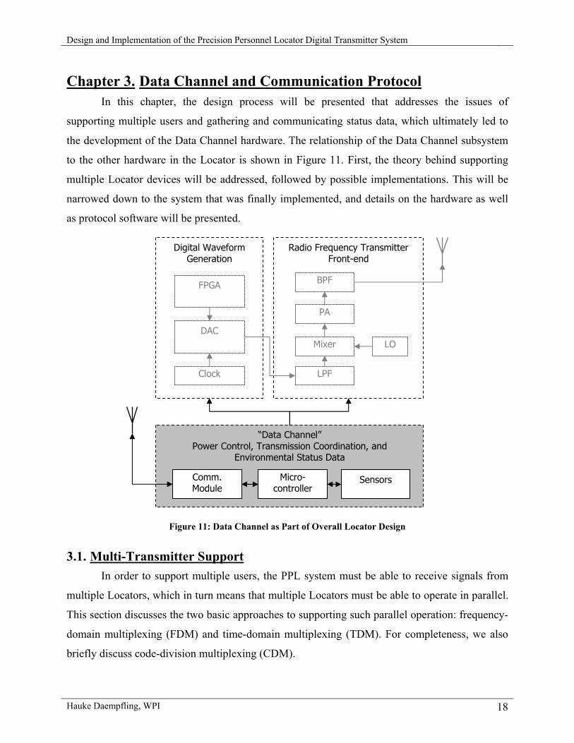
Chapter 3. Data Channel and Communication Protocol In this chapter, the design process will be presented that addresses the issues of
supporting multiple users and gathering and communicating status data, which ultimately led to
the development of the Data Channel hardware. The relationship of the Data Channel subsystem
to the other hardware in the Locator is shown in Figure 11. First, the theory behind supporting
multiple Locator devices will be addressed, followed by possible implementations. This will be
narrowed down to the system that was finally implemented, and details on the hardware as well
as protocol software will be presented.
Figure 11: Data Channel as Part of Overall Locator Design
3.1. Multi-Transmitter Support In order to support multiple users, the PPL system must be able to receive signals from
multiple Locators, which in turn means that multiple Locators must be able to operate in parallel.
This section discusses the two basic approaches to supporting such parallel operation: frequency-
domain multiplexing (FDM) and time-domain multiplexing (TDM). For completeness, we also
briefly discuss code-division multiplexing (CDM).
“Data Channel” Power Control, Transmission Coordination, and
Environmental Status Data
Digital Waveform Generation
Radio Frequency Transmitter Front-end
Comm. Module
Micro-controller
Sensors
FPGA
DAC
LPF
Mixer
PA
BPF
LO
Clock
Design and Implementation of the Precision Personnel Locator Digital Transmitter System
Hauke Daempfling, WPI 19
In TDM, the Locators, or simply transmitters (as their main function is to transmit the
ranging signal), do not actually transmit in parallel, but a “virtual parallelism” is achieved by
having the transmitters transmit for short durations in rapid succession. An overview of this
situation with four transmitters, T1 through T4, is shown in Figure 12. The major advantage of
this approach is that it is very straightforward to implement, and can be used to conserve power
as well, as the transmitter’s duty cycle is much reduced. However, this requires the circuitry to be
able to power on and off quickly, otherwise this power-saving advantage disappears. In addition,
a trade-off must be made between the minimum time to transmit for each transmitter, number of
transmitters in the system, and messaging frequency. This means that this approach may require
the active coordination of the transmitters, depending on the restrictions on clock drift, which will
be discussed in detail in later sections.
Figure 12: Time-Division Multiplexing
In FDM, the different transmitters transmit at different frequencies, allowing for
concurrent operation. This is theoretically possible because the PPL signal consists of individual
carriers, each of which takes theoretically zero bandwidth. Figure 13 shows two approaches: on
the left, the different transmitters’ carriers are consecutive and use completely different frequency
bands; on the right, the different transmitters’ carriers are interleaved.
Figure 13: Frequency-Domain Multiplexing, Bands (left) vs. Interleaving (right)
T1
T2
T3
T4
t
f f
Design and Implementation of the Precision Personnel Locator Digital Transmitter System
Hauke Daempfling, WPI 20
The advantage to this approach is that one does not have to worry about turning a
transmitter on and off and coordinating between different transmitters, so no control hardware is
needed for these tasks. However, there are also several disadvantages. This approach is harder to
implement on both the transmitter and receiver: The transmitter has to span a larger number of
possible transmission frequencies, while the receiver has the added task of dissembling the
received signal into its different transmitter components. Also, and most importantly,
implementing such a system for a large number of transmitters (up to 100) with the current
waveform (at least 50 carriers) means that five thousand carriers would have to fit in a frequency
range limited by the bandwidth of the receiver, which may only be a few hundred MHz. Such
tight packing of the waveform carriers may lead to other problems, such as a reduction of the
multipath-resistant characteristics of the ranging signal due to the chance of different transmitters
interfering with each other (for example through clock drift or harmonics). Hence, it may be that
in order to support the targeted number of transmitters (100), the system would have to employ
some kind of control hardware to manipulate the transmitted signals to prevent interference,
similar to what is needed for TDM, which eliminates this advantage of FDM and raises the
question of whether it would not just be simpler to only implement TDM.
A final approach that is used for multiplexing data together is CDM (also known as
CDMA, or code-division multiple access), the very basic idea of which is that two transmitters
transmit at the same time and on the same frequencies, and only by a special encoding scheme
can a receiver recover the data transmitted from each source. One of the disadvantages of this
scheme is that the transmit power of each unit must be closely controlled, otherwise one
transmitter might “drown out” another. However, the major disadvantage is that for our purposes,
it is unacceptable to overlap two different carriers, as this disrupts the phase information that is
required for the range estimation. Therefore, it is clear the CDM is useful only for binary data
transmission and not for our system.
In conclusion, while FDM may offer advantages for systems with a smaller number of
transmitters, it is clear that TDM is the best approach due to its simplicity. The following section
investigates this multiplexing method.
3.2. Time-Division Multiplexing In time-division multiplexing, it is clear that the transmitter’s emissions must be
controlled so that no two transmitter’s transmissions overlap. For example, the system
Design and Implementation of the Precision Personnel Locator Digital Transmitter System
Hauke Daempfling, WPI 21
specifications state that 100 transmitters should be able to provide location updates once a
second, so each transmitter has only 10 ms to transmit. In this section, we will verify that TDM is
indeed feasible in this situation, and then discuss different schemes that allow this kind of control.
We will verify that our goal of multiplexing 100 transmitter units to provide updates once
a second is realistic, considering that each transmitter only has 10 ms to transmit. There are
several factors to keep in mind: whether this time allows for enough of the ranging waveform to
be transmitted, how much data can be transmitted during this time (assuming some kind of data
communication is taking place), and whether this provides a tight enough resolution for tracking.
The current signal consists of “symbols” of 8192 samples, sampled at 200 MSPS, which
gives a symbol period of 40.96 µs. This allows for 244 symbols to be transmitted in a 10 ms
period. Although the capture of a single symbol is sufficient for range estimation, multiple
symbols can be “time fused” to provide better SNR: each doubling of the number of symbols
gives a SNR boost of about 3 dB. However, one must keep in mind that clock drift might cause
transmitters to drift, which means a guard time should be implemented in the beginning and end
of the 10 ms period – this will be discussed in detail in the following section. Therefore, while a
balance between the number of symbols transmitted and the required guard time has to be found,
we can assume that 10 ms is sufficient time to transmit a ranging signal.
Assuming that some kind of data communication other than the transmitters’ ranging
signal waveforms is implemented, we can quickly calculate that at a relatively slow baud rate of
19.2 kbits/second, 24 bytes could be transferred in a 10 ms period. For a simple control/command
protocol, this may be sufficient, but may not be if larger amounts of data needed to be transferred.
This issue will be discussed in more detail in a later section, but one can see that this time period
does allow for a transfer of a small amount of data.
Finally, we would like to know what resolution an update rate of once per second gives.
A human walks at a normal rate of about 1.2 m/s [15] (for reference, the fastest human running
speed is about 10 m/s [10], while a human falling at terminal velocity is about 60 m/s [9]), and
we can assume that a firefighter who is loaded down by heavy gear may not walk as quickly. In
addition, firefighters often crawl along the floor, below any smoke that may be in the air, further
reducing their rate of movement. So, we can see that a position update of once per second should
give a resolution of better than one meter. In addition, we can imagine that a future system might
be able to dynamically adjust the number of updates per second depending on the actual number
Design and Implementation of the Precision Personnel Locator Digital Transmitter System
Hauke Daempfling, WPI 22
of users that require accurate tracking. This would mean that certain users’ positions (such as
those who are outside the building or who are not moving often) could be updated less frequently,
resulting in a higher resolution for other users. Similar variations on this scheme to further
increase accuracy could also be implemented, but in general, a tracking resolution of typically
better than one meter is on the order of the overall system accuracy and is therefore sufficient.
We must now discuss methods with which to implement a TDM scheme. There are many
medium access control schemes in existence for communications on shared mediums, such as
ALOHA, Slotted Time (with beacons or shared clocks), Carrier Sense Multiple Access (CSMA)
with Collision Avoidance or Detection, Bit-Map or Binary Countdown protocols, and so on [25].
Current widely used communications standards such as Wireless LAN (802.11 [12]), Bluetooth
(802.15.1 [5]) or ZigBee (802.15.4 [33]) all use variations of the previously listed medium access
control methods. However, these protocols all have one thing in common that make them
unsuited for direct application to the current system: they assume that every station is a
transceiver, or at the very least a transmitter with the capability to detect communications or
collisions on the medium.
The previous generation of transmitter/receiver hardware allowed only for one-way
communication. The multi-carrier waveforms were generated on the transmitter by feeding data
from a static memory inside an FPGA into a DAC, and on the receiver end, the waveforms were
digitized by an ADC and FPGA and transferred to a MATLAB script to extract the range
information. This means that modulating or in any way actively manipulating the generated
waveform on the transmitter side would involve complex calculations and therefore complex
hardware on the transmitter FPGA. Another issue is the power question: the transmitter chain of
FPGA plus DAC plus RF front-end consumed on the order of many hundred milliamps, and
constantly running this system would require a large battery or the run time would be reduced to
unacceptably. Similarly, the receivers in this system required a large amount of hardware (RF
front-end, ADC, etc.) that make it unfeasible to add receiver hardware to each transmitter.
Therefore, it is clear that the previous version of transmitter hardware was only fitting to generate
a ranging signal waveform and not for bi-directional or data communication.
Therefore, in the following two sections, we will investigate the question of how a system
in which the transmitters have no receive capability might function.
Design and Implementation of the Precision Personnel Locator Digital Transmitter System
Hauke Daempfling, WPI 23
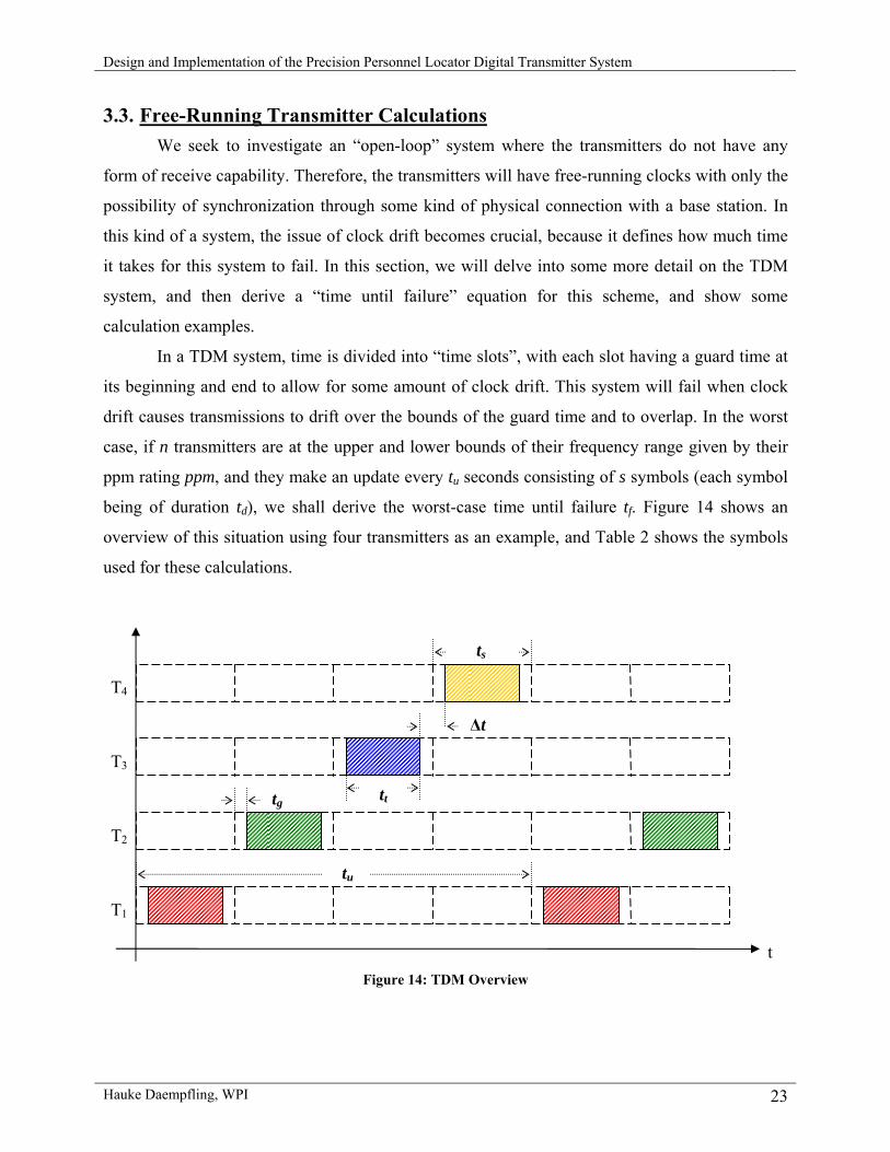
3.3. Free-Running Transmitter Calculations We seek to investigate an “open-loop” system where the transmitters do not have any
form of receive capability. Therefore, the transmitters will have free-running clocks with only the
possibility of synchronization through some kind of physical connection with a base station. In
this kind of a system, the issue of clock drift becomes crucial, because it defines how much time
it takes for this system to fail. In this section, we will delve into some more detail on the TDM
system, and then derive a “time until failure” equation for this scheme, and show some
calculation examples.
In a TDM system, time is divided into “time slots”, with each slot having a guard time at
its beginning and end to allow for some amount of clock drift. This system will fail when clock
drift causes transmissions to drift over the bounds of the guard time and to overlap. In the worst
case, if n transmitters are at the upper and lower bounds of their frequency range given by their
ppm rating ppm, and they make an update every tu seconds consisting of s symbols (each symbol
being of duration td), we shall derive the worst-case time until failure tf. Figure 14 shows an
overview of this situation using four transmitters as an example, and Table 2 shows the symbols
used for these calculations.
Figure 14: TDM Overview
T1
T2
T3
T4
t
tu
tg tt
∆t
ts
Design and Implementation of the Precision Personnel Locator Digital Transmitter System
Hauke Daempfling, WPI 24
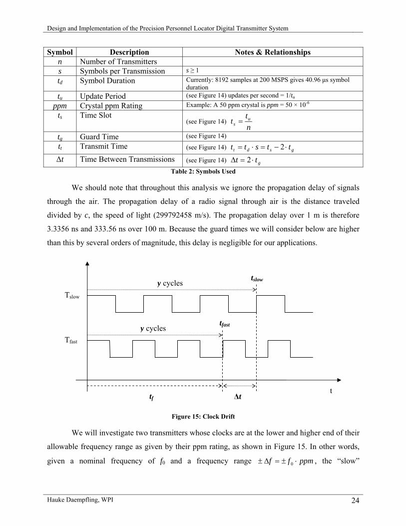
Symbol Description Notes & Relationships n Number of Transmitters s Symbols per Transmission s ≥ 1 td Symbol Duration Currently: 8192 samples at 200 MSPS gives 40.96 µs symbol
duration tu Update Period (see Figure 14) updates per second = 1/tu
ppm Crystal ppm Rating Example: A 50 ppm crystal is ppm = 50 × 10-6 ts Time Slot
(see Figure 14) nt
t us =
tg Guard Time (see Figure 14) tt Transmit Time (see Figure 14) gsdt ttstt ⋅−=⋅= 2
∆t Time Between Transmissions (see Figure 14) gtt ⋅=∆ 2
Table 2: Symbols Used
We should note that throughout this analysis we ignore the propagation delay of signals
through the air. The propagation delay of a radio signal through air is the distance traveled
divided by c, the speed of light (299792458 m/s). The propagation delay over 1 m is therefore
3.3356 ns and 333.56 ns over 100 m. Because the guard times we will consider below are higher
than this by several orders of magnitude, this delay is negligible for our applications.
Figure 15: Clock Drift
We will investigate two transmitters whose clocks are at the lower and higher end of their
allowable frequency range as given by their ppm rating, as shown in Figure 15. In other words,
given a nominal frequency of f0 and a frequency range ppmff ⋅±=∆± 0 , the “slow”
t
tslow
tfast
∆t
Tfast
Tslow y cycles
y cycles
tf
Design and Implementation of the Precision Personnel Locator Digital Transmitter System
Hauke Daempfling, WPI 25
transmitter’s (Tslow) clock frequency is fslow = f0 – ∆f and the “fast” transmitter’s (Tfast) clock
frequency is ffast = f0 + ∆f.
After y clock cycles, Tslow and Tfast will “think” they are at the same point in time,
however their actual times (the times at which they actually complete y clock cycles) are,
respectively, ff
ytslow ∆−=
0
and ff
yt fast ∆+=
0
. We are interested in the point in time when the
difference in these two times, ∆t = tslow – tfast, grows too large, because at this time the guard time
will be overstepped and transmissions will begin to overlap. Since the “fast” transmitter will
cause an error (overlapping transmission) first, this point in time is tfast, and we shall call this the
time until failure, tf.
Using the above information, we derive tf as follows. First, we will combine the above
equations for the difference in the two clocks:
ppmffy
ppmffyt
⋅+−
⋅−=∆
0000
Solving ppmff
ytt fastf ⋅+==
00
for y and substituting:
( ) ( )ppmff
ppmfftppmff
ppmfftt ff
⋅+
⋅+⋅−
⋅−
⋅+⋅=∆
00
00
00
00
Simplifying and solving for tf:
ppmppmtt f ⋅
−⋅∆=
21 Equation 1
Now we would like to express this time until failure in terms of the system parameters
ppm, n, s, td, and tu (see Table 2). We can derive an expression for ∆t using the relationships
given in Table 2 as follows:
Solving gsd ttst ⋅−=⋅ 2 for gt⋅2 and substituting into gtt ⋅=∆ 2 :
sttt ds ⋅−=∆
Substituting the given equation for ts:
sttn
t du ⋅−⋅=∆1
Finally, inserting this into the above equation for tf:
Design and Implementation of the Precision Personnel Locator Digital Transmitter System
Hauke Daempfling, WPI 26
ppmppmstt
nt duf ⋅
−⋅⎟⎠⎞
⎜⎝⎛ ⋅−⋅=
211 Equation 2
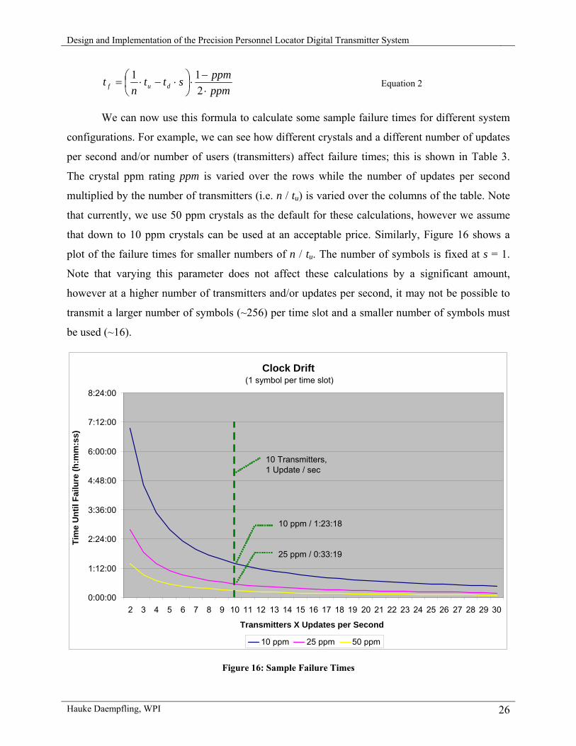
We can now use this formula to calculate some sample failure times for different system
configurations. For example, we can see how different crystals and a different number of updates
per second and/or number of users (transmitters) affect failure times; this is shown in Table 3.
The crystal ppm rating ppm is varied over the rows while the number of updates per second
multiplied by the number of transmitters (i.e. n / tu) is varied over the columns of the table. Note
that currently, we use 50 ppm crystals as the default for these calculations, however we assume
that down to 10 ppm crystals can be used at an acceptable price. Similarly, Figure 16 shows a
plot of the failure times for smaller numbers of n / tu. The number of symbols is fixed at s = 1.
Note that varying this parameter does not affect these calculations by a significant amount,
however at a higher number of transmitters and/or updates per second, it may not be possible to
transmit a larger number of symbols (~256) per time slot and a smaller number of symbols must
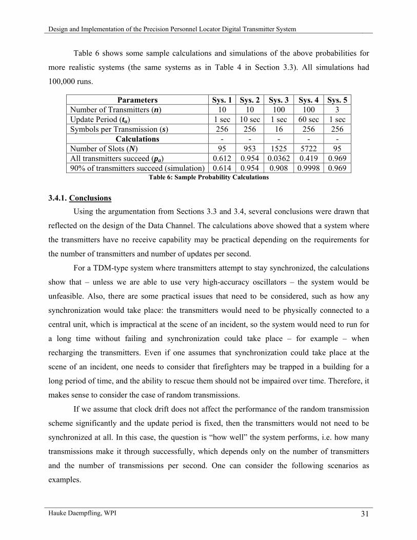
Calculations - - - - - Number of Slots (N) 95 953 1525 5722 95 All transmitters succeed (pa) 0.612 0.954 0.0362 0.419 0.969 90% of transmitters succeed (simulation) 0.614 0.954 0.908 0.9998 0.969
Table 6: Sample Probability Calculations
3.4.1. Conclusions
Using the argumentation from Sections 3.3 and 3.4, several conclusions were drawn that
reflected on the design of the Data Channel. The calculations above showed that a system where
the transmitters have no receive capability may be practical depending on the requirements for
the number of transmitters and number of updates per second.
For a TDM-type system where transmitters attempt to stay synchronized, the calculations
show that – unless we are able to use very high-accuracy oscillators – the system would be
unfeasible. Also, there are some practical issues that need to be considered, such as how any
synchronization would take place: the transmitters would need to be physically connected to a
central unit, which is impractical at the scene of an incident, so the system would need to run for
a long time without failing and synchronization could take place – for example – when
recharging the transmitters. Even if one assumes that synchronization could take place at the
scene of an incident, one needs to consider that firefighters may be trapped in a building for a
long period of time, and the ability to rescue them should not be impaired over time. Therefore, it
makes sense to consider the case of random transmissions.
If we assume that clock drift does not affect the performance of the random transmission
scheme significantly and the update period is fixed, then the transmitters would not need to be
synchronized at all. In this case, the question is “how well” the system performs, i.e. how many
transmissions make it through successfully, which depends only on the number of transmitters
and the number of transmissions per second. One can consider the following scenarios as
examples.
Design and Implementation of the Precision Personnel Locator Digital Transmitter System
Hauke Daempfling, WPI 32
In a live demonstration version of the system, it would be desirable to have a fairly high
update rate (once per second), but a large number of transmitters would not be required. In this
case, the calculations show that it seems feasible to have free-running transmitters.
For a production-level system, a higher number of transmitters is required (100). The
calculations show that a system with a high number of updates (once per second) would not
perform very well. The possibility exists of offering a lower-cost version with, for example, a
lower number of updates (such as every 60 seconds), but this does not meet the production level
system requirements of providing real-time tracking of Locator units. In any case, the random
transmission scheme would always involve some transmissions colliding.
From these arguments, it became clear that to be able to coordinate a large number of
transmitters and updates per second, only a system where the transmitters can be coordinated
wirelessly in some kind of TDM scheme gives a high reliability. There are several advantages to
designing transmitters with added receiver or transceiver capability, including the fact that such a
capability could always be dropped later to offer a lower-cost and lower-performance version of
the system as discussed above.
Other advantages of such a system are, for example, that a higher level of control is
possible over the transmitters. Transmitters could be turned off remotely to conserve power when
not at the scene of an incident, and the number of updates per second and number of transmitters
could be reconfigured on-the-fly. Transmitters would not need to encode a unique ID into their
transmitted signal and receivers would not need to be able to detect overlapping transmissions. In
addition, other data could be transmitted over the extra communication channel, such as device
status or environment or physiological information.
It was clear from these arguments that the realization of the Data Channel was justified.
In the following sections, we will discuss the implementation of the Data Channel.
3.5. Bi-Directional Communication As we can see from the previous sections, in order to achieve the full functionality of the
Locator units, a system capable of communicating on a channel separate from the ranging
waveforms had to be designed. First, the option of a “receive only” functionality on the Locator
units was investigated, which would reduce the cost of the units. Then, both standardized and
custom different bi-directional communications systems were investigated. This section discusses
these design decisions.
Design and Implementation of the Precision Personnel Locator Digital Transmitter System
Hauke Daempfling, WPI 33
In order to keep the Locator units simple and therefore cheaper, we can imagine a system
where each Locator unit is equipped only with a transmitter for the ranging signals and a receiver
for the command and control communications. While such a system would provide enough
functionality for basic TDM operation and power control, there would be no direct way for the
Locator to relay data back to the Base Station, such as status information or at the very least a
device ID. However, this information could theoretically be “piggybacked” onto the transmitted
ranging waveform. Since the ranging signal follows a traditional OFDM structure, data could be
modulated onto this signal (a common technique in communications systems). However, it is
clear that adding a system that modulates the transmitted ranging waveform would add a
relatively large amount of complexity, as compared to simply giving the Locators a separate, bi-
directional communications channel via a separate transceiver module, as we will see below.
There are several existing, widely used communications standards that were briefly
considered. Wi-Fi (IEEE 802.11, [12]) has an average (indoor) range of about 30 m, and latencies
in the tens of ms [4, 14]. Bluetooth (IEEE 802.15.1, [5]) is a protocol for “personal area
networks”, and with a maximum output power of 100 mW, can theoretically cover distances of
100 m. However, one of the downsides of both these communications standards is that they
require relatively large protocol stacks and are in most cases not suitable for prototype
implementation. Finally, ZigBee (IEEE 802.15.4, [33]) is a relatively new protocol for close-
range communications (10-75 m), which may not be enough for our purposes. In addition, at the
time this system was being designed, there was not yet a wide selection of ZigBee transceivers
and stack implementations available, indicating that the technology might not be mature yet.
For our applications, it seemed that using these existing communications standards would
be “overkill”, so simpler transceiver IC’s and modules were investigated. A broad search of
different vendors’ offerings showed that there are several similar products available that operate
in the license-free 433 MHz and/or 900 MHz bands. Table 7 shows a summary of the most
promising modules.
The ChipCon CC1100 seemed the most advanced of the chips as it supports internal
buffers, automatic generation of checksums, automatic receive polling, received signal strength
indicator (RSSI), and a standardized SPI interface to communicate with the chip. However, the
maximum transmit power it supports is 10 dBm, and there was concern that this would not be
able to cover enough distance. Initial tests with evaluation boards showed that the coverage from
Design and Implementation of the Precision Personnel Locator Digital Transmitter System
Hauke Daempfling, WPI 34
a vehicle parked outside a large building (such as Atwater Kent Laboratories at WPI) may not be
able to cover the full building (a range of about 100m).
Product Freq. Range (MHz)
Data Rate
Output Power
Receiver Sens. Interface Notes
ChipCon CC1020
402-408, 804-940
153.6 kbps
-20 to 10 dBm
-118 dBm Sync. Digital
ChipCon CC1100
300-348, 400-464, 800-928
500 kbit/s -30 to 10 dBm
-110 dBm SPI & Others
with buffers, CRC, etc.
Atmel AT86RF211S
400-480, 800-950
100 kbps 15 dBm -107 dBm Sync. Digital
better documentation than ChipCon
Xemics DP1205
868-870, 902-928
152.3 kbit/s
15 dBm -113 dBm Sync. Digital
Complete module with external components
Micrel MICRF505
850-950 200 kbps 10 dBm -97 dBm Sync. Digital
Table 7: Transceiver Modules
There are two transceivers with a higher output power than the ChipCon transceivers, and
one of these, the Xemics DP1205, stood out because it is a complete solution in a small, shielded
module that includes the Xemics XE1205 transceiver IC and all necessary passive components. It
does not support all the advanced features of the CC1100, but still includes a smaller buffer (16-
byte, vs. 64-byte buffer in the CC1100) for burst transmissions and support for automatic
transmission detection and synchronization with the incoming bit stream. While this module is
not as advanced as the ChipCon variant, it supports all the basic necessary features and supports a
higher output power, so it was decided that this module should be used in the design.
3.6. Hardware Specifications The Data Channel Hardware development began in late 2005. At the time, a functioning
TDM control hardware was required to be completed for a demonstration of a multi-transmitter
system in mid-2006, so outside contractors were hired to speed the development and design the
details of the Data Channel hardware and provide basic firmware. This section describes the
specifications for the PPL Data Channel hardware that were used to develop the new hardware.
Figure 18 shows a conceptual block diagram of the transmitter as it existed at the time (before the
development of the new Digital Waveform Generator hardware also described in this thesis) and
the proposed Data Channel hardware.
Design and Implementation of the Precision Personnel Locator Digital Transmitter System
Hauke Daempfling, WPI 35
Figure 18: General Locator Block Diagram
Several decisions on details of the design were made before the final specifications were
established. The most important of these was the selection of the TI MSP430 microcontroller
family as the microcontroller in the system. This decision was made because the MSP430F161x
family is a very low-power microcontroller that had been used in previous, similar designs. The
following is a list of the specifications for the Data Channel hardware.
Transceiver
Microcontroller
Accelerometer
Debug
(Pin Headers, LEDs, RS23)
Antenna
Xilinx Virtex-2 FPGA On TX: DAC On RX: ADC DDRAM
RF Front-End
Antenna
Existing PPL RF Hardware
PPL Data Channel Hardware
Temp. Sens.
Distress Btn.
Design and Implementation of the Precision Personnel Locator Digital Transmitter System
Hauke Daempfling, WPI 36
• Conceptual Tasks
o Coordinate and control TDM of Locator transmissions
o Manage power of entire Locator device
o Monitor and communicate “environmental data” (movement, temperature, distress
button)
• PCB Layout
o System should fit on a PCB with dimensions of 2.5 x 3 inches.
o Mounting holes must be compatible with existing boards.
• Power
o System should include a low-power voltage regulator that provides 3.3 V to power
the entire Data Channel hardware.
o System should have the capability of being powered from a DC power supply or
conventional batteries (AA/AAA).
o The components in this system must either be low-power (<1mA), have the ability
to be put into a low-power “sleep mode”, or to be powered off in some other
fashion.
• Wireless
o System must support wireless communication with a Xemics DP1205 module.
o Minimum Range: 100m indoors
o Minimum Data Rate: approx. 10 kbps
o Must be FCC compliant and support Frequency Hopping Spread Spectrum
(FHSS)
o Interface of transceiver must provide for low-latency communications – i.e.
interrupts generated on reception of packets and streaming data output
• Microcontroller
o System must include Texas Instruments MSP430F1611 microcontroller
o Must include JTAG interface for programming
• Accelerometer
o System must include an accelerometer to detect non-movement of device
o Accelerometer should be at least two-axis for better general movement
measurement
Design and Implementation of the Precision Personnel Locator Digital Transmitter System
Hauke Daempfling, WPI 37
• Distress Button
o System must include a pushbutton connected to the microcontroller (to trigger
transmission of a distress signal)
o Suggested to connect to a microcontroller port capable of generating interrupts
(MSP430 ports P1 and P2)
• Temperature Sensor
o System must be able to measure ambient temperature
• Interface
o System must be able to interface to existing hardware (operates at 3.3 V)
o Several pin headers (about 16) connected to microcontroller ports required;
suggested: MSP430 ports P1 and P4. These pin headers should be laid out as
groups of eight pin headers with a ground connection at each end (ten pins to a
row).
o System must have a way to configure a board ID (such as through a rotary DIP
switch), can be shared with microcontroller ports
• Debugging
o System must provide RS232 interface
o System must provide test points, pin headers and status LEDs
o Suggested to include an additional pushbutton for user input
• Firmware
o Code must be written in C, compatible with IAR compiler
o Low-level drivers for interfacing to the Xemics DP1205 and the Accelerometer
will be provided.
Figure 19 shows a block diagram that represents many of these specifications, and shows
how the components of the Data Channel system were connected. Note that in addition to the
items listed here, a simple graphical user interface (GUI) on a PC for test and debug of the units
was implemented.
Design and Implementation of the Precision Personnel Locator Digital Transmitter System
Hauke Daempfling, WPI 38
Figure 19: Data Channel Hardware Block Diagram
3.7. Hardware Implementation The Data Channel boards were designed, ordered and populated during February and
March 2006. Although parts of the circuit design, the schematic entry and PCB layout were done
by outside consultants, all other tasks were done at WPI. The WPI tasks included the overall
design as described in the previous section, selection of the major parts in the system, basic
circuit design, parts ordering, board assembly and testing. A total of ten boards were completed
and tested to be functional (please see the Experimental Results chapter for details). Figure 20
shows a completed Data Channel board. In this section, some of the elements of the Data
Channel hardware will be described.
TI MSP430 Microcontroller
Xemics DP1205 Transceiver
Module
Analog Devices Accelerometer
(w/ conditioning interface)
LEDs
Temperature Sensor
Pin Headers & Rotary DIP
Antenna SMA Connector
Voltage Regulator (3.3V, powers all
blocks shown here)
Battery DC Power Supply
RS232 Interface
Distress Button
Antenna
PPL RF HW (3.3V)
Test & Debug
Design and Implementation of the Precision Personnel Locator Digital Transmitter System
Hauke Daempfling, WPI 39
Figure 20: Completed Data Channel Hardware
In general, the design of the Data Channel hardware corresponds to the block diagram
shown in the previous section (Figure 19). The functionality of the Xemics module [32] is
described in Section 3.9 on the implementation of the protocol, and in this section, we will
describe some of the other noteworthy features of the boards.
The MSP430F1611 microcontroller [16] has a total of six I/O ports, many of which are
shared with other functions, such as USARTs or a built-in analog-to-digital converter. Along with
three pin headers that connect directly to three different MSP430 ports, the microcontroller also
interfaces to the Xemics module through one of its USARTs in SPI mode, to an RS232 level
shifter through the second USART, and to the temperature sensor through an SPI interface that is
implemented with general-purpose I/O. In addition, the battery voltage is applied to one of the
pins of the built-in ADC through a voltage divider (so as not to overload the input pin) so that the
code on the MSP430 is capable of determining the current battery voltage.
The only crystal on the board is a 32.768 kHz crystal, which drives the MSP430. The
MSP430 features a “digitally controlled oscillator” (DCO), which is a digital PLL that multiplies
the basic clock up to a much higher frequency, so it can be used as a fast instruction clock. In our
implementations, we chose a 4 MHz instruction clock to allow for near-maximum speeds.
However, we chose to operate the timers, which are also an important feature of the MSP430, to
Distress Button
Acceler-ometer
Transceiver Module
PC Interface
Temperature Sensor
Micro-controller
Interfaceto other
Hardware
Design and Implementation of the Precision Personnel Locator Digital Transmitter System
Hauke Daempfling, WPI 40
run of the 32.768 kHz crystal, to avoid any problems with PLL jitter and to be able keep the CPU
timers operating while the CPU is put into a low-power mode. The timers operate by running a
counter to which a number of “capture and compare” modules are connected. In essence, these
modules trigger an interrupt when certain timer values are reached (a “tick”), and they can
therefore be used to time multiple different events off a single, continually running timer.
The MSP430 supports several different low-power modes that allow for disabling of
different parts of the CPU such as the DCO, the CPU core itself, and other oscillators in the
system. These modes can be entered from software, and can be exited by different events such as
a timer tick (if the timers are enabled during the low power mode) or an event on the RS232
receive line. Note that the boards are typically powered by three AA batteries that can be installed
in a batter holder in the back of the PCB.
The movement detection circuitry (also referred to simply as the “analog” circuitry
because it is the only analog circuitry on the board) features an Analog Devices ADXL330
accelerometer [23]. A special movement detection circuit was designed; it is shown in Figure 21.
This circuit takes the output of each of the axes of the accelerometer, which is a voltage that is
proportional to the acceleration of the IC and first low-pass, then sums and high-pass filters it.
The effect of this circuit is that the voltage at the “ACC” output generally rests at about 1.5V,
except when there is movement, in which case the output voltage changes, but still quickly settles
back to the nominal output if there is no more acceleration. As a result, one must merely watch
the output of this circuit, which feeds directly into one of the microcontroller ADC pins, for
changes, and if any changes are observed, this indicates movement. This circuitry has the ability
to be powered down via a control signal from the microcontroller, to conserve power when it is
not in use.
As the boards were being completed, development on the firmware that was provided by
the outside contractors was continued. Several of the drivers that had been provided had to be
rewritten for efficiency and bug fixes, such as the drivers to interface for the Xemics radio
module, and the driver for RS232 communication with the PC. The firmware was written and
compiled in IAR Systems Embedded Workbench for the TI MSP430.
Because the Data Channel is actually a very general platform, providing wireless
communications, a low-power microcontroller, expansion ports, and a PC interface, it was also
used for several other purposes in supporting the PPL system and experiments. For example,
Design and Implementation of the Precision Personnel Locator Digital Transmitter System
Hauke Daempfling, WPI 41
code was written that interfaces it to a variable gain amplifier on the PPL receiver boards; to an
Analog Devices PLL chip, and to analog switches that control RF input from multiple antennas.
Most notably however, the Data Channel was also interfaced to the newly built Digital Waveform
Generators in order to test the functionality of the power control of those boards, and eventually
the entire Locator device.
Figure 21: Data Channel Movement Detection Circuit
Having built this hardware as described in the previous sections, we will now describe
protocol that provides the Time-Division Multiplexing scheme described earlier.
3.8. Communications Protocol In order for the Data Channel units to communicate amongst one another and accomplish
the tasks set forth in the previous sections, a wireless communications protocol must be
developed. It is important to note that the focus of the project work changed after the Data
Channel hardware development had been completed in mid-2006, and supporting multiple
transmitters received a lower priority than other developments. Because, among other things,
using the Data Channel as a general platform for supporting the PPL project became more
important than a full protocol implementation, note that only a proof-of-concept of the protocol
framework described in this section was implemented, as is described in the subsequent section.
Design and Implementation of the Precision Personnel Locator Digital Transmitter System
Hauke Daempfling, WPI 42
Although the Data Channel hardware will eventually be merged with the hardware of the
entire Locator device, the boards were designed separately from the other prototype parts of the
system. Figure 22 shows an overview of the concept of how the Data Channel units fit into the
system. Both Locator units (LU) and Reference Units (RU) are each given a Data Channel board
(DC). The first “layer” of communication is the Reference Units communicating with the
Locators. The second layer of communication is the Base Station communicating with the
Reference Units. In the future, this second layer can be implemented through a high-speed link,
such as 802.11. However, in the proof-of-concept implementation, the major goal was to show
that the “time slot” TDM system is functional, so only one layer of communications was
implemented and only one Data Channel board is present at the Base Station, instead of one at
each Reference Unit. This concept can then be extended, as the Reference Units only function as
a “relay” or “repeater” for the data that is communicated between the Locators and the Base
Station, as will be described below.
Figure 22: System Overview
RU DC
RU DC
RU DC
BS
LUDC
802.11
OFDM
DCP
BS = Base Station RU = Reference Unit LU = Locator Unit DC = Data Channel
DCP = Data Channel Protocol
LUDC
LUDC
LUDC
Design and Implementation of the Precision Personnel Locator Digital Transmitter System
Hauke Daempfling, WPI 43
Because the correct functioning of the ranging signal transmission is essential, the Data
Channel’s main responsibility is providing TDM control for the Locator devices. This is achieved
by receiving time-synchronizing information from the units outside the building. The other data,
namely commands for the Locator units and status information, is included with the time
synchronization.
As we have seen in the previous sections, 100 Locator units in the system communicating
once a second gives each unit a 10 ms time slot within which to communicate, both for their Data
Channel and for their ranging signal transmission, although these do not necessarily need to
happen in the same slot. In the proof-of-concept system, only sixteen time slots were
implemented, because only ten Data Channel boards were built initially and the rotary DIP switch
used to encode the board ID has only sixteen positions. However, the slot length was kept at 10
ms, and the number of slots can easily be increased by adjusting the configuration of the
firmware.
Because it is important for the Locators to conserve power, an important feature for the
Data Channel units is to be able to be wirelessly commanded to power down. As we have seen
from the hardware description, the Data Channel boards have the ability to go into a very low-
power sleep mode out of which they can be awakened by timer interrupts. We can assume that
the Data Channel is capable of powering on and off the rest of the Locator sections and
controlling ranging signal transmissions through its expansion ports with the same accuracy as it
can control its own timings and power. We will assume that this “sleep mode” feature can be
implemented by programming the Data Channel to regularly wake up and listen for any wireless
commands to power itself up and return to normal operations.
3.8.1. Data Format In order to describe the protocol, we must first know what data we are communicating.
The data that needs to be sent from the Locators to the Base Station (via the Reference Units) are:
distress signal, movement data, temperature, diagnostics, and acknowledge for previously sent
commands. Data from the Base Station to the Locators would be mainly power commands. In
addition, we will assume that a Data Channel board can synchronize its timer to the reception of a
packet, which we will refer to as a synchronization packet or synchronization signal. Note that
this packet can include regular data as well. The implementation details are described in the
Design and Implementation of the Precision Personnel Locator Digital Transmitter System
Hauke Daempfling, WPI 44
subsequent section. We will now describe a framework data packet format for the communication
of this information.
First, we must determine the possible size of the packet. Because the time available in
which to communicate is limited by the slot length, the data rate is a limiting factor. As the
Experimental Results chapter will show, the optimal baud rate for the boards is 19200 baud. At
this rate, the maximum number of bytes that can be transmitted in 10 ms is 24 bytes. If we
assume 1 ms guard time at either end of the slot, this reduces to 19 bytes that can be transmitted
in each slot. We will keep this in mind in the following discussion to and determine if this is
sufficient to transmit all necessary data.
The Xemics module provides for the detection of a preamble of alternating ones and
zeroes and a unique identifier of up to four bytes, which also serves as a synchronization pattern
to align the incoming bit stream into bytes. The suggested preamble length is 3 bytes, and for our
purposes, we would like to avoid false pattern detection in random noise, so we will use the
maximum identifier length of four bytes. While these bytes have to be manually inserted at the
transmitter, the Xemics module automatically detects and strips these bytes at the receiver.
During testing of the modules, it was determined that even when radio conditions are
good, single-bit errors may still occur in packets. Therefore, it was decided to implement a
forward error correction scheme using a (12,8) Hamming code, which can correct single-bit
errors. The use of this code increases the number of bits necessary to encode a message by 50%
(i.e. one byte of parity information for every two bytes of data), but allows for one bit error in
every twelve bits of data. In addition, to further reduce the chances of errors occurring in the case
of the Hamming code failing, a “checksum” byte consisting of a byte-by-byte XOR of the
contents of the packet is appended prior to Hamming encoding. Any packets received that show
errors can be discarded. Both the Hamming Code and the checksum are applied to the payload of
the packet, which does not include the preamble and unique identifier. Although Hamming
encoding normally involves interleaving the check bits into the data, for ease of implementation
we will merely append the check bits to the end of the packet, giving one byte of check bits for
every two bytes of data.
As will be shown in detail below, the Reference Units do not communicate directly
amongst one another, and the Locators do not communicate amongst one another, but every
Reference Unit receives every packet from every Locator and vice versa. Therefore, an
Design and Implementation of the Precision Personnel Locator Digital Transmitter System
Hauke Daempfling, WPI 45
addressing scheme to uniquely identify each unit only requires a “source” address, which can be
a single byte consisting of the board’s unique ID. Furthermore, the unique identifier implemented
in the Xemics module can differ for transmissions from Locators to Reference Units and vice
versa, so that accidental communication amongst Reference Units and amongst Locators can be
avoided. Therefore, the destination of a packet is always clear.
Finally, we must encode the data into the remaining bytes of the packet. Table 8 shows
the data that must be transmitted from Locator to Base Station, and Table 9 shows the data that
must be transmitted from Base Station to Locator. As we can see, the communications require
only three bytes of payload for either communication in addition to the one-byte address, the one-
byte checksum and the Hamming parity data. Because the Hamming code is more efficient for an
even number of bytes to encode, an additional “reserved” byte can be added to the payload,
which could later be used for other psychological status or other data. Figure 23 shows the
resulting packet, which is 16 bytes long and can be transmitted in 6.67 ms. One should note that
if required, two more payload bytes could be added, resulting in one more Hamming byte and a
total packet length of 19 bytes, which can be transmitted in 7.92 ms. Therefore, our assumptions
on baud rate being fast enough and the length of the guard time are shown to be acceptable.
Field Size Description User Distress Signal 1 bit Distress signal triggered by user Temperature Alert 1 bit Automatic distress for high temperature Non-Movement Alert 1 bit Auto. distress on non-movement detection Low Battery Alert 1 bit Warning for low battery voltage Diagnostics 3 bits Reserved for diagnostic codes to indicate
other hardware problems Acknowledge 1 bit Acknowledges the receipt of a command Ack. Packet Identifier 1 byte Packet identifier of the packet which
contained the command being ack’ed Temperature 1 byte Temperature value in Celsius
(-40 to 150 deg C) Table 8: Data from Locator to Base Station
Field Size Description Packet Identifier 1 byte Unique packet identifier Target Locator ID 1 byte The ID to which a command is being
sent (if any) Power Up Command 1 bit Tells a sleeping Locator to power up Power Down Command 1 bit Tells a Locator to go to sleep Alert/Distress Ack. 1 bit Acknowledges reception of alerts
Table 9: Data from Base Station to Locator
Design and Implementation of the Precision Personnel Locator Digital Transmitter System
In general, when a unit is attempting to receive a packet, it attempts to do so over most of
the duration of the slot. A receive timeout of 9500 µs was selected, because it leaves 500 µs or
time for 330 to 2000 instructions in the slot. Transmitting 17 bytes takes 7175 µs, which leaves
2325 µs guard time in the slot, which is sufficient for our implementation, which specifies at least
2 ms guard time total (1 ms at each end of the slot). An overview of this situation is presented in
Figure 26.
Figure 26: Timeslot Overview
10 ms Slot
9500 us Rx Window
7175 us Tx Time (17 bytes)Grd. Grd.
Design and Implementation of the Precision Personnel Locator Digital Transmitter System
Hauke Daempfling, WPI 53
The board that is acting as the Reference Unit remains in receive mode for most of the
duration of a “cycle” of 16 times 10 ms, or 160 ms. This also means that for most slots, there is
no switching penalty from the Xemics module mode switching because the module can simply
stay in receive mode. Reception can be timed to begin exactly at the beginning of the slot, and the
transmitting board can implement the 1 ms guard time. Every time a reception is initiated, the
Xemics firmware drivers must write to the Xemics module registers, which takes about 160 µs,
so the timer must be set to tick 160 µs early for all slots except slot 0.
In slot 0, the synchronization signal transmitted by the Reference Unit must arrive at the
Locators at the exact time of the beginning of slot 0 – this of course means that the actual time
that the timer ticks on the Reference Unit must be adjusted so that it begins transmitting early.
The timings, which are as follows, are illustrated in Figure 27.
• Xemics mode switch from receive to transmit (labeled “Rx to Tx” in figure) = 150 µs
(timed exactly by MSP430 timers)
• Time to initialize transmission = 80 µs (estimated time to write 2 bytes to Xemics buffer);
included in figure together with the switching time above
• Time to transmit pattern and unique identifier bytes (“Sync”) = 3270 µs (measured)
• Over-the-air delay (“Air”) = 136 µs (measured)
This gives a total time of 3636 µs – this is how much earlier the Reference Unit must
begin its transmission process compared to the beginning of slot 0. This means that, as previously
mentioned, no communication can happen in slot F; however, a workaround to this limitation is
described later. After the Reference Unit has transmitted the synchronization signal, the
following things will happen in the beginning of slot 0:
• Transmit remaining 10 bytes of packet (“Data”) = 3905 µs (measured and calculated)
• Time to switch Xemics module back to receive mode (“Tx to Rx”) = 600 µs (timed
exactly) – this is so that at the beginning of slot 1, the Reference Unit is already in receive
mode and there is no mode switching penalty.
• Total time used in slot 0: 4505 µs – this leaves 5495 µs in the slot, which could even be
used for additional data from the Reference Unit to the Locators.
Design and Implementation of the Precision Personnel Locator Digital Transmitter System
Hauke Daempfling, WPI 54
Figure 27: Synchronization
Figure 27 also shows the implementation of the Locator Units’ timings. One must keep in
mind that as opposed to the Reference Unit, the Locator spends most of its time in sleep mode to
conserve power, so one must take into account the longer Xemics module mode switching times.
In slot 0, the Locator knows that it can expect a synchronization signal at the beginning of the
slot. In order to receive this signal, the Locator must wake up early, during what is actually slot F,
to prepare to receive the synchronization and data packet. These timings are as follows:
• Wake-up time to receive (labeled “to Rx” in figure) = 2850 µs (timed exactly by MSP430
timers)
• Time to initialize reception = 160 µs (estimated time to write 4 bytes to Xemics buffer);
included in figure together with the switching time above
• Guard time in case Reference Unit transmission starts early (“Guard”) = 1000 µs (timed)
• Time to receive 7 bytes of pattern plus unique identifier (“Sync”) = 3270 µs (measured)
• Over-the-air delay = 136 µs (measured); not shown in figure
This means the Locator needs to wake up a total of 7416 µs before the beginning of slot 0.
Logically, this also means that slot 0 is extended by 7416 us, which the Locator needs to adjust
for when resetting its timer. As with the Reference Unit, in slot 0, the time it takes to receive 10
bytes is 3905 us (measured), leaving 6095 us in the slot (no mode switch time to sleep). Again,
one should note that no communication can take place in slot F, since all boards will be busy
mode-switching.
RU:
Slot F (10 ms) Slot 0 (10 ms)
Sync DataIdle (Rx) Idle (Rx)
Rx to Tx
AirTx to Rx
Sleep to Rx Sync Data Sleep
Guard
LU:
Design and Implementation of the Precision Personnel Locator Digital Transmitter System
Hauke Daempfling, WPI 55
When a Locator unit needs to transmit data in its slot, it should begin transmitting 1 ms
into the slot to implement the guard time. However, to wake up from sleep it takes a total of 2430
µs; therefore, it must actually wake up from sleep and initialize transmission 1430 µs before the
beginning of the slot it should transmit in. With a transmit time of 7175 µs for 17 bytes of data,
that means the Locator will be done transmitting 8175 µs into the slot – which should give it
enough time (1325 µs) before the Reference Unit times out on the previously described 9500 µs
receive timeout. This situation is shown in Figure 28.
Figure 28: Data Transmission
As previously mentioned, this protocol implementation is limited in that it does not allow
transmissions in the final slot; this is due to the Reference Unit having to switch from receive to
transmit mode and then transmitting a synchronization packet, which cuts into the time available
in that slot. One can see that with this implementation, this problem would still exist even when
expanded to 100 Locators. However, there are several approaches to solving this problem. For
example, one might note that, considering the results of the Data Channel boards’ timing
accuracy, the guard time of 1 ms could be reduced by a slight amount without impacting the
performance of the system, and this could be used to allow for enough time for mode switching.
Alternatively, one could imagine a system where there are 101 slots for the Data Channel, and
only 100 for ranging signal transmissions, meaning that although the Data Channel and ranging
signal transmissions would not be aligned for most of the time, the ranging signal transmissions
would still allow for updates to be provided once a second. The impact of increasing the Data
Channel cycle time to 1.001 s should not be noticeable to the user.
RU:
LU:
Slot N-1 (10 ms) Slot N (10 ms)
Sleep to Tx Tx
Sleep
Idle (Rx) Idle (Rx)To Rx
Rx Rx
Design and Implementation of the Precision Personnel Locator Digital Transmitter System
Hauke Daempfling, WPI 56
Finally, it should be mentioned that this “time shifting” of the 10 ms time slot timer ticks
is not the only method for synchronizing all units. An alternative that was tested and confirmed
to work is using yet another Data Channel board as a dedicated “beacon”, the only task of which
is to provide regular synchronization packets for all boards in the system. This method works
well for experimental setups, but one must consider that in a real-life scenario such a beacon
would have to be able to communicate with all Data Channel boards in the system (both on
Reference Units and in Locators inside the building), which does not match with assumptions
previously made about Locators not always being in range of all units outside the building.
Overall, and as the Experimental Results chapter will confirm, this proof-of-concept
implementation of the protocol showed that the time-division multiplexing of Locator’s ranging
signal transmissions can be managed by the Data Channel boards.
Design and Implementation of the Precision Personnel Locator Digital Transmitter System
Hauke Daempfling, WPI 57
Chapter 4. Digital Waveform Generation The waveform used for the ranging signals in the PPL project is one that is not practical
to produce using analog methods; therefore, it is clear that a digital approach to generating this
waveform must be taken. This approach has the added benefit that new waveforms can be created
and generated without any hardware changes, and in theory, this approach could even be used to
dynamically modify waveforms on the fly. Figure 29 shows the relationship of the waveform
generation subsystem to the rest of the Locator device.
Figure 29: Digital Waveform Generator as Part of Overall Locator Design
The previous version of waveform generation hardware (see Section 2.3 for details) used
a Xilinx Viretx-2 field programmable gate array (FPGA) and an Analog Devices AD9736 digital
to analog converter (DAC), with an FPGA storing the waveform in its block RAM and providing
a data clock and the data to the DAC over LVDS lines using DDR clocking. Although this
method may be appropriate, the prototype boards that implemented it are relatively large because
they feature extra components, take too much power and are in general “overkill” for the current
requirements.
“Data Channel” Power Control, Transmission Coordination, and
Environmental Status Data
Digital Waveform Generation
Radio Frequency Transmitter Front-end
Comm. Module
Micro-controller
Sensors
FPGA
DAC
LPF
Mixer
PA
BPF
LO
Clock
Design and Implementation of the Precision Personnel Locator Digital Transmitter System
Hauke Daempfling, WPI 58
To design new waveform generation hardware, several design decisions had to be made.
The major ones were that new DAC was selected and a way to provide it with data was devised,
and these decisions must be made with size, power control, and other factors such as low turn-on
times (for time-division multiplexing) in mind. Figure 30 shows a block diagram of the concept
of this hardware.
Figure 30: Digital Waveform Generator Concept
This chapter presents the redesign of the Digital Waveform Generator hardware. The
following sections will discuss the selection and design of these parts of the system. This is
followed by details on the implementation of the new generation of hardware.
4.1. Digital-to-Analog Converter Design The selection of an appropriate DAC is crucial because it is one of the two major
components of the waveform generator system, and must fit the specifications as well as possible.
The DAC to be used on the new boards had to be capable of generating signals of a bandwidth of
up to 150 MHz, meaning a 300 MSPS sampling rate, at a resolution the same as or, optimally,
better than the current DAC, which supports 14 bits. Other criteria were a low noise profile and
enough output power to provide at least -40 dBm per subcarrier. In addition, the data interface
was an important selection criterion, as it determines the range of different data generation
circuits that the DAC can be connected to.
The two major vendors for DACs that were investigated were Maxim and Analog
Devices, as they are both known for their large selection of analog parts, and the parts had
DAC
Clock Generation
Data Supplying System
to RF Front-end
“Analog” Section“Digital” Section
Digital Ranging Signal
Waveform Data
Design and Implementation of the Precision Personnel Locator Digital Transmitter System
Hauke Daempfling, WPI 59
previously been used by members of the PPL team. Other vendors (such as Macom or National)
were also investigated but no suitable parts were found.
Maxim offers only a handful of DACs within the desired sampling frequency range. The
only DACs with sampling rates at 300 MSPS or above were specified as 500 and 600 MSPS,
available in both 14 and 16-bit variety, with an LVDS interface. Of these, the DAC that best fits
the parameters is the MAX5888, a 16-bit, 500 MSPS DAC with an LVDS data interface, good
analog performance characteristics, and a relatively low power consumption of about 44 mA at
100 MSPS sampling rate [2].
Analog Devices offers a larger range of higher-frequency DACs, however again there is
only a smaller number of DACs available that match the given parameters. For example, the
AD9755 is a 14-bit, 300 MSPS DAC, with the advantage of having two data ports that accept
data at half the sampling rate, which allows for much easier interfacing. However, it is
recommended to select a DAC that has a somewhat higher sampling frequency than the one
needed to produce the bandwidth for the desired signal, as this will avoid any problems with
running the part at its nominal top speed, and will avoid spurious components from the clock
signal on the output. Another possible part was the AD9726 [1], which is a 400 MSPS, 16-bit
DAC with an LVDS data interface, and very similar analog performance characteristics as the
MAX5888. We will compare this part to its Maxim counterpart in more detail.
The Maxim part has a relatively simple interface; it has only one clock input and single
data rate data inputs, which means they sample their data at each rising edge of the clock signal.
The Analog part has a more involved interface, with two clock inputs, one for the overall DAC
sampling clock and one for the DAC data, and one clock output, which can be used to feed the
device that is providing the data. In addition, it features a serial peripheral interface (SPI) that
gives access to some internal configuration registers, such as the DAC calibration. In terms of
current consumption, the Maxim part is clearly better with only about 44 mA drawn from a single
3.3 V supply (at 100 MSPS sampling rate), while the Analog part requires a 2.5 V and a 3.3 V
rail, and it draws a total of about 209 mA (at 400 MSPS sampling rate). See Table 11 for a
summary of the DAC comparison to this point.
Design and Implementation of the Precision Personnel Locator Digital Transmitter System
Hauke Daempfling, WPI 60
Feature MAX5888 AD9726 Sampling Rate 500 MSPS 400 MSPS Resolution (bits) 16 bits 16 bits Interface LVDS, SDR LVDS, SDR and DDR Clocks single sampling clock sampling clock in, data clock out,
data clock in Power 44 mA at 100 MSPS
3.3 V rail 209 mA at 400 MSPS 2.5 V and 3.3 V rails
Start-up time 10 ms 5 – 20 ms Additional Features - SPI interface for configuration,
clock synchronization Table 11: DAC Comparison
It seems that the Maxim part would be optimal simply due to its lower current
consumption; however, the Analog part has two additional features that make it superior. The
AD9726 supports double data rate (DDR) data transfer, which has the advantage that the circuitry
supplying the data can be optimized in such a fashion that it only needs to run at half the
sampling rate (details will be shown in the following section). Most importantly however, the
Analog part features an internal clock synchronization system. While the data flowing into the
DAC must be aligned to the data clock, the sampling clock can have any phase relation to the
data clock, and as long as the two clocks are at the same frequency, the DAC will automatically
align the data to the sampling clock correctly. These separate clock inputs provide for much more
flexibility, because systems supplying data to the DAC should be able to more easily supply their
own, correctly aligned data clock with the data, instead of attempting to align their data to the
already existing sample clock. These advantages make it clear that the AD9726 is the better DAC
for this design.
4.1.1. Sampling Clock Having selected this DAC for our system, we must turn our attention to another important
aspect regarding the DAC, which is the generation of the sampling clock. For this purpose, a
design was proposed with the assistance of an outside consultant; it is illustrated in Figure 31.
This design is based on a circuit currently in use on several PPL RF front-end boards to generate
the local oscillator clocks, and on one of two recommended clock configurations from the DAC
datasheet. This design is based on a voltage-controlled oscillator (VCO) that is controlled by an
Analog Devices ADF4110 integer phase-locked loop (PLL). The output of this circuit is then fed
through a 1:4 transformer in order to boost the voltage levels. At the DAC, the differential inputs
Design and Implementation of the Precision Personnel Locator Digital Transmitter System
Hauke Daempfling, WPI 61
are high impedance, so the signal must be biased appropriately (1.25V) and terminated with the
appropriate impedance (200 Ω is used instead of 50 Ω due to the 1:4 transformer). The DAC
requires a minimum differential voltage of 0.5 V, which this circuit was expected to provide.
Figure 31: Proposed DAC Clock Generation Circuit
An advantage of this design was that it can be adapted for different sampling frequencies.
The VCO has a certain range of frequencies it can be tuned to by the PLL IC. In addition, the
VCO can be exchanged for other models that provide different frequencies. For this design, the
Sirenza VCO191-220U and VCO191-294U were chosen as alternatives, as they provide
frequency ranges of 210-230 MHz and 279-308 MHz, respectively. For the implementation, the
VCO191-220U and a sampling frequency of 220 MSPS was initially chosen, as a higher
sampling frequency was not yet required.
Unfortunately, when the first boards had been populated, it was determined that the
circuit did not provide the voltage levels that were expected as they are labeled in the figure
above, and the minimum differential voltage of the clock signal required by the DAC inputs was
not reached. A solution to this problem was sought, and a modification to the above circuit was
developed based on the second of the two clock configurations recommended in the DAC
datasheet. This configuration involves the addition of an active LVPECL driver, which outputs
ADF4110 PLL Loop Filter VCO10 MHz
Ref. Clk.
ADC-10-4 Coupler
Approx -1 dBm, 0.56V p-p
1:4 Transformer 1:1 Transformer
~0.8 V
DAC
200 Ω
1.25V
Clock+
Clock-
Design and Implementation of the Precision Personnel Locator Digital Transmitter System
Hauke Daempfling, WPI 62
voltage levels appropriate for the DAC. Luckily, this modification could be implemented using a
MAX9375 “Anything-to-LVPECL Translator”, which accepts differential or single-ended signals
with as little as 100 mV swing and up to 2 GHz frequency. This IC could be mounted on the
board in place of the 1:1 transformer, as shown in Figure 32, and with some modifications to the
associated passive components, the clock circuit was made fully operational. These modifications
can be included in a new revision of the hardware.
Figure 32: Modifications to Clock Circuit
The DAC and the supporting clock generation circuitry represent the “analog” portion of
the Digital Waveform Generator, and we will now turn our attention to the purely digital portion
of the system.
4.2. Data Supplying System Design In designing a system to supply data to the digital-to-analog converter, there were several
factors that had to be kept in mind. The most important of these was speed and power – the
circuitry needed to provide data at up to 300 MSPS while still consuming less power than the
current hardware. A factor in conserving power was for the circuit to have low turn-on and turn-
off times, as this allows for a lower duty cycle. Two possible designs were considered. The first
was to use the existing design idea of an FPGA providing the data. The second alternative was to
use a high-speed memory combined by a small amount of logic, for example a CPLD, to control
the memory. This section describes the selection process for this part of the design.
FPGAs are generally regarded as problematic in low-power applications because they are
perceived to have long turn-on times and high current consumption. Most larger FPGAs are
LVPECL Driver
1:4 Transformer
DAC Clock Inputs
Design and Implementation of the Precision Personnel Locator Digital Transmitter System
Hauke Daempfling, WPI 63
volatile, meaning they do not store their configuration when powered down, which in turn means
that they require external PROM chips that they must load their configuration from whenever
they are powered on, which can take a relatively long time (on the order of several hundred
milliseconds or more). In addition, FPGAs can draw on the order of several hundred mA or more
while running. Therefore, an alternative solution was sought.
4.2.1. High Speed Memory and CPLD The major alternative to FPGA-based designs was a system in which data is supplied
directly from a non-volatile random-access memory. In such a system, some kind of address
counter would be needed to control the address lines of the RAM, and a way to load a waveform
into the RAM would be needed as well. This makes it clear that a smaller custom logic device
such as a CPLD would be necessary. CPLDs have the additional advantage that they are usually
nonvolatile, meaning they stay configured even when power is turned off and they power on very
quickly. However, research into existing CPLD devices shows that despite these advantages,
suitable devices are not available. A search across manufacturers such as Xilinx, Altera, Atmel,
Cypress, Lattice Semi, Actel and Quicklogic showed that CPLDs offered generally have an I/O to
speed tradeoff, the limits of which are just under the requirements for this system. This is due in
part by the fact that the CPLDs researched do not support DDR, which means they must run at
the full system speed of 300 MSPS. In addition, most common standalone memories, such as
those available from Cypress or Micron, are not available in a size/speed combination that is
appropriate for our applications. For example, the faster synchronous SRAMs offered by Cypress
are available only at a minimum size of 9 MB, and a maximum speed of 250 MHz. The amount
of data that needs to be supplied is small compared to this: 8192 16-bit samples give a total size
of 131072 bits or 16 kilobytes. Finally, most of these SRAMs require on the order of several
hundred milliamps while running, very similar to what an FPGA would consume. Therefore, it
becomes clear that a “CPLD and RAM” solution may be too impractical and inflexible, and an
FPGA solution would be optimal if its shortcomings can be overcome.
4.2.2. Field Programmable Gate Array At WPI, the most experience has been gathered with FPGAs from Xilinx, and available
support and experience are a large factor in deciding what vendor to choose. However, a search
of some of the same manufacturers listed above, such as Altera, Lattice Semi and Quicklogic,
Design and Implementation of the Precision Personnel Locator Digital Transmitter System
Hauke Daempfling, WPI 64
was made in order to determine what alternatives are offered by other manufacturers. In general,
it appeared that the two manufacturers with the largest selection of FPGAs, Xilinx and Altera,
actually have very similar offerings. For example, the Altera Cyclone series is very similar to the
Xilinx Spartan series, and the Altera Stratix is similar to the Xilinx Virtex family in terms of size
and speed, and most other features. Because of these similarities, it was appropriate to choose the
Xilinx families, as they were already well-supported at WPI. These parts were investigated with
respect to size, power, and speed.
As mentioned earlier, the major problem perceived with volatile FPGAs their
configuration time when powered up. This is because most FPGAs are configured to use a serial
configuration interface, and are commonly not run at their maximum possible configuration rate.
However, most Xilinx FPGAs support an 8-bit parallel configuration interface called
“SelectMAP” which can operate at speeds of up to 50 MHz. If we select a relatively small FPGA
so that the configuration bitstream is kept small, such as from the Spartan-3 family, we can
reduce the configuration times to acceptable rates. Figure 33 shows a table of configuration times
for different Xilinx parts. Referring to the Spartan-3 datasheet [24], we see that the smallest
FPGA that supports enough Block RAM for our purposes is the part XC3S200, with 216 Kbits.
This FPGA can be configured in as little as 2.62 ms, which suits our purposes very well. Some
work was done to confirm these configuration rates by measuring configuration times on a
Spartan-3 demo board, which showed that at a 5 MHz configuration clock, serial configuration
took 209 ms, which matches well with the times given in the table, which show configuration
times at 50 MHz clock speed.
Figure 33: Xilinx Spartan-3 Configuration Times (Source: Xilinx XAPP452)
Design and Implementation of the Precision Personnel Locator Digital Transmitter System
Hauke Daempfling, WPI 65
Next, it was investigated whether the XC3S200 is capable of operating at speeds fast
enough to support our 300 MSPS operation. A test design for logic to supply waveform data was
implemented in the Xilinx design environment based on the final design that is described in
Section 4.3.3. This design operates using double data rate transmission, requiring the maximum
clock speed in the design to be only half the sampling rate. Using the Spartan-3 datasheet and the
Xilinx design tools, it was determined that the maximum speed that the design could run at was
212 MHz. This shows that the Spartan-3 is indeed capable of operating fast enough, if we assume
DDR operation. In fact, we see that theoretically, operation of up to 400 MSPS (the limit of the
DAC), or 200 MHz DDR clock rate, would be supported by this design, which is much more than
the required 300 MSPS. As the Experimental Results chapter will show, this was indeed possible.
Finally, the expected current draw by this design was considered. Using a combination of
the datasheets and the Xilinx XPower tool, we the design used for testing above was analyzed.
For this design, the XC3S200 was estimated to draw about 329 mA. While this value seems high,
one must consider that due to the short configuration times of the FPGA, a low duty cycle can be
achieved. If we assume that we will be using the “10 ms time slot” system developed in Chapter
3, and we estimate a start-up time of the digital section of about 5 ms (which includes the FPGA
configuration time of 2.62 ms), we see that the duty cycle of the FPGA circuitry can be reduced
to as little as 1.5%. This will be discussed in detail in Section 5.2.2.
One should note that Xilinx offers a “low-power” version of their Spartan-3 FPGAs,
known as Spartan-3L, which generally are very similar to the Spartan-3 series except that they
draw somewhat lower currents, and have a special “hibernate” mode. However, if one reads the
datasheets in detail, the advertised “hibernate” mode is nothing more than actually powering off
the FPGA. The smallest device in this series is the XC3S1000L, which has five times the logic
resources of the XC3S200, resulting in a longer configuration time, and some of the current-
saving advantages are lost. In addition, these devices are only available as ball grid array
packages, which we would like to avoid, as we will see below. Therefore, it seems that the
XC3S200 was indeed the optimal choice.
4.2.3. FPGA Configuration In order to support the SelectMAP parallel configuration, the Xilinx XCF-P series
PROMs must be used. The smallest of these is the XCF08P, which can hold up to 8 Mbits of
configuration information. Although this is relatively large compared to the required bitstream
Design and Implementation of the Precision Personnel Locator Digital Transmitter System
Hauke Daempfling, WPI 66
size of about 1 Mbit, it is the smallest available PROM that supports SelectMAP configuration
and therefore the advantage of faster configuration is greater than that of some wasted resources.
New designs can be programmed into this PROM using the provided JTAG programming
interface, which is also supported by the FPGA and the Xilinx tools. Although the PROM
features the ability to generate a configuration clock, in order to achieve the highest possible
configuration rate of 50 MHz, an external oscillator must be used to drive the PROM (which in
turn provides the configuration clock to the FPGA). Adding a 50 MHz oscillator also has the
advantage of being able to route this clock signal to the FPGA for use as a system clock in cases
where the DAC’s clock is not functional.
4.2.4. Package Selection The XC3S200 is available in four different package options, ranging from a 100-pin quad
flat pack to a 256-pin ball grid array package. While the larger packages generally support a
higher package density and a higher user I/O count, the have the disadvantage that one cannot
mount them by hand, or debug or modify them without difficulties. Therefore, it was decided that
the smallest possible package should be used. Two limiting factors in this case are the number of
available I/O pins, and the support for simultaneously switching outputs (SSO). SSO guidelines
state that in order to prevent large ground bounce, the number of simultaneously switching pins
per pair of VCCO-GND connections on the package must be limited. For the smallest available
package, known as VQ100, and the LVDS standard, this limit is seven switching pin pairs per I/O
bank. As the banks of the VQ100 package only support three or four pairs of LVDS pins, this
limitation should not affect this package. However, one must take care when judging the total
number of I/O pins available. The VQ100 package has many pins with dual functions, such as
some pins for “digitally controlled impedance” (DCI), or for reference voltages for specific I/O
standards, or for configuration. Although our design uses no DCI or I/O standards that require
reference voltages, we must keep in mind that by using the parallel SelectMAP configuration, we
are occupying more pins than a serial configuration would. Subtracting the pins needed for
configuration and the power supply and ground pins, there are 51 user I/O pins remaining. In our
design, we require at least 18 differential pairs to connect to the DAC (16 data and two clock
lines), and we see that this requirement is satisfied. Finally, it is important to note that because
the design will be operating close to the speed limitations of the FPGA, one should select the
latest revision of the FPGA (Rev. E) and the highest available speed grade (-5) for best
Design and Implementation of the Precision Personnel Locator Digital Transmitter System
Hauke Daempfling, WPI 67
performance in terms of items such as slew rate, DCM performance, and LVDS I/O standard
performance.
Having selected the major components of the system, the FPGA and the DAC, details of
the design of the Digital Waveform Generator hardware will now be presented.
4.3. Hardware Implementation In this section, some of the details of the hardware design of the Digital Waveform
Generator boards will be presented, including issues such as power control, interfaces, PCB
layout, and FPGA design.
Figure 34 shows an overview of the components in the Digital Waveform Generator. The
most important of these, i.e. the FPGA, configuration PROM, DAC, and DAC clock generation,
have already been discussed in previous sections. As is apparent from this diagram, the power
distribution for this board is somewhat complex, as there are several different supply voltages
required by the DAC and FPGA. In addition, it was decided to separate the power supplies of the
analog and digital portions of the board in order to avoid noise passing between these parts of the
board; these will be referred to as the “analog” and “digital” portions of the system, as shown in
the figure. The power system will be discussed in more detail below.
An element of this diagram that has not previously been mentioned is the level shifter. It
was decided to include a MAX3001E bi-directional level shifter because the FPGA’s I/O banks
are operating on 2.5 V, and it will most likely be necessary to interface to hardware that operates
on higher voltage levels, such as the Data Channel hardware or the digital interfaces of the DAC
and PLL, which all operate on 3.3 V. The level shifter is connected to a total of eight free pins on
the FPGA. A 3.3 V supply line can even be passed from the analog power supply to the level
shifter. This has the advantage that the FPGA can program registers as necessary on the DAC and
the PLL without the need for an external board, such as the Data Channel, performing this task.
Design and Implementation of the Precision Personnel Locator Digital Transmitter System
Hauke Daempfling, WPI 68
Figure 34: Digital Waveform Generator Block Diagram
4.3.1. Power Supply Design
An important feature of the waveform generation hardware is to save power by shutting
down when it is not needed. Therefore, special attention must be paid to the power distribution
system of the board. There are several voltages required by the different components of the
board: the FPGA requires 1.2 V and 2.5 V, the PROM requires 1.8 V and 2.5 V, and the DAC
and various other components require 2.5 V and 3.3 V. We would like to be able to power down
the PROM separately from the FPGA when it is not needed. In addition, the 50 MHz oscillator
that supplies the configuration clock to the PROM should optionally stay enabled when the
PROM is powered down, in case it is being used as a system clock for the FPGA as well. Figure
35 shows a distribution system for the digital components of the system that accommodates these
requirements. For the analog components in the system, shown in Figure 36, no special
Xilinx Spartan-3 XC3S200 FPGA
VQ100 Rev E
-5
XCF08P Config. PROM
JTAG
SelectMAP
Power 1.2 V, 1.8 V,
2.5 V
AD9726 DACPower 2.5 V, 3.3 V
300 MHz Clock
LVDS Data
Transformer
SMA to RF
SPI
LEDs
Pin Header
LVDS Clk
Level Shifter
2.5 – 5 V
SPI
8 Data
LPF (optional)
50 MHz Clock
“Digital” portion
“Analog” portion
Design and Implementation of the Precision Personnel Locator Digital Transmitter System
Hauke Daempfling, WPI 69
separation of the power supplies is needed, because all components of the analog system will be
enabled together during normal operation.
Figure 35: Digital Side Power Distribution
Figure 36: Analog Side Power Distribution
We see from this design that a total of four regulators are required for the digital portion
and two regulators are required for the analog portion. Table 12 shows estimates of current
50 MHz Osc
2.5 V
FPGA VCCINT 1.2 V
FPGA VCCO 2.5 V
PROM 1.8 V
PROM 2.5 V
Level Shifter
1.2 V Regulator
2.5 V Regulator
External (2.5 to 5
V)
Jumper
FPGA VCCAUX
2.5 V
2.5 V Regulator
1.8 V Regulator
Main Power Supply
Regulator Enable Lines
2.5 V Regulator
Main Power Supply
3.3 V Regulator
DAC 2.5 V
DAC 3.3 V
DAC Clock 3.3 V
Regulator Enable
Design and Implementation of the Precision Personnel Locator Digital Transmitter System
Hauke Daempfling, WPI 70
consumption values that we can use to judge what current flow these regulators must support.
Note that some elements of the system were not included, such as debug LEDs, or the level
shifter (which consumes only about 1 mA). In addition, some of the estimates in this table are
based on tools such as the Xilinx XPower analysis tool, and may change as the design is changed.
Therefore, we must design with a safety margin in mind in case a component draws more current
than expected.
Device Voltage Typ. (mA) Max. (mA)FPGA 1.2 V 57 80 FPGA 2.5 V 272
50 MHz Osc. 2.5 V 30 PROM 1.8 V 10 PROM 2.5 V 40
DAC Clock 3.3 V 15 18 DAC 2.5 V 141 158 DAC 3.3 V 68 78
Table 12: Current Consumption Estimates
Table 13 shows the regulators that were chosen based on these requirements. Each of
these regulators features an individual enable line. It was decided to tie together the enable lines
for the analog section, as all components will be powered on together, as previously mentioned.
In addition, the enable lines for the PROM were tied together. The FPGA enable lines were left
separate because one of the regulators has an active high enable line, while the other has an active
low enable line. In addition, it is recommended to enable the FPGA’s 2.5 V supply before
enabling the 1.2 V supply to prevent current surges [24]. The four resulting enable lines are
brought out on a pin header to allow the required power sequencing to be generated by an
external source, such as the Data Channel board.
Power Supply Regulator Max. CurrentFPGA 1.2 V TI TPS76912 100 mA FPGA 2.5 V TI TPS79525 500 mA PROM 1.8 V TI TPS76918 100 mA PROM 2.5 V TI TPS76925 100 mA Analog 2.5 V Analog 3.3 V
TI TPS71202 (dual-channel)
250 mA (each channel)
Table 13: Regulator Selection
Design and Implementation of the Precision Personnel Locator Digital Transmitter System
Hauke Daempfling, WPI 71
4.3.2. PCB Design As previously mentioned, it was decided to separate the analog and digital portions of the
waveform generation hardware in order to prevent electrical noise leaking between the two
portions, especially to prevent digital switching noise from leaking to the analog components. To
this end, it was decided to also physically separate the two sections of the design onto two sides
of the PCB being designed. This has the advantage that with a multi-layer PCB, ground planes
can be used to protect the two sides from noise. It was decided to implement a six-layer PCB for
optimal separation and to route the many signal and control lines. The layers were defined as
follows:
• Layer 1 (Top): Digital components and routing
• Layer 2: Digital power and some routing
• Layer 3: Ground plane
• Layer 4: Analog power and some routing
• Layer 5: Ground plane
• Layer 6 (Bottom): Analog components and routing, also flooded with ground copper
This separation of the layers gives another advantage. Both the DAC and the FPGA
packages are of the quad flat pack style, with 80 and 100 pins, respectively. The only connections
passing between the analog and digital side, other than the main power supply and the previously
mentioned connection to optionally supply 3.3 V to the level shifter from the analog side (which
is heavily decoupled), are the LVDS connections to and from the DAC – sixteen data pairs and
two clock pairs. Investigating the pin layout of the packages, which are shown in Figure 37, it is
clear that the possibility exists to mount the two devices directly “back-to-back” on the top and
bottom layer of the PCB in order to minimize the length of the traces.
This approach was taken, and it was possible to route all LVDS lines in this fashion.
Figure 38 shows a part of the finished layout, in which several trace pairs (circled in dashed lines)
routed in close quarters between the FPGA and the DAC can be seen. It is important to keep the
lengths of all LVDS lines very similar, in order to minimize skew across the data and between the
individual pairs themselves. The trace length across all LVDS lines was measured to be
approximately 275 ± 69 mils, which is small enough to prevent any skew problems.
Design and Implementation of the Precision Personnel Locator Digital Transmitter System
Hauke Daempfling, WPI 72
Figure 37: DAC and FPGA Packages
Figure 38: Routed LVDS Data Lines
The only downside to choosing this layout is that placing decoupling capacitors close to
the pins of the FPGA and DAC was more difficult because of the large number of traces that
must be routed away from the IC’s pins before any capacitors can be placed. Under normal
circumstances, the decoupling capacitors would be placed on the underside of the board as close
LVDS
LVDS
Clocks
Clocks
Output
Config.
DAC FPGA
Design and Implementation of the Precision Personnel Locator Digital Transmitter System
Hauke Daempfling, WPI 73
to the pins as possible, but with this design that is clearly not possible. However, care was taken
to place the decoupling capacitors as close to their power and ground pins as possible.
Figure 39 shows the top “digital” side of a completed Digital Waveform Generator PCB.
One can see the FPGA in the bottom right and the PROM in the bottom left portion of the board.
The three SMA connectors are connections for supplying an external 10 MHz reference for the
PLL, supplying an alternative input for the DAC clock (such as via a signal generator), and the
DAC output. The pin headers on the board interface to such things as the PLL and DAC’s SPI
ports, the board’s JTAG chain, and the level shifter, which is connected to the FPGA.
Connections from the FPGA to the SPI interfaces of the PLL and DAC can be established simply
by placing a jumper cap on the respective pins of the two ten-pin headers that can be seen at the
left of the board.
Figure 39: Completed Digital Waveform Generator Board, Top (Digital) Side
Figure 40 shows the bottom “analog” side of a completed Digital Waveform Generator
PCB. One can see the DAC is on the lower left, with the clock generation circuitry occupying the
upper half of the board.
FPGA PROM
Level Shifter
Power Control Interface
Design and Implementation of the Precision Personnel Locator Digital Transmitter System
Hauke Daempfling, WPI 74
Figure 40: Completed Digital Waveform Generator Board, Bottom (Analog) Side
4.3.3. FPGA Digital Design Finally, we will describe the design of the hardware that is instantiated inside the FPGA
that generates the waveform data for the DAC. The basic principle of the hardware is that the
waveform data is loaded from a block memory, which is controlled by an address counter that is
simply an up counter. However, we must support speeds of up to 300 MSPS, and this requires
DDR operation in the FPGA. In this type of data transfer, data is provided on both the rising and
the falling edge of the clock signal, which therefore has half the frequency of the sampling rate.
This is illustrated in Figure 41.
Figure 41: DDR Timing Diagram (Source: AD9726 Data Sheet)
DAC
DAC Clock Generation
DAC Output
Design and Implementation of the Precision Personnel Locator Digital Transmitter System
Hauke Daempfling, WPI 75
DDR can be implemented with a special type of flip-flop that is supported in hardware by
the Spartan-3 series, which accepts two data and clock signals that are 180 degrees out of phase,
and outputs a data stream consisting of the two “merged” data signals by sampling each data
input at the rising edge of its respective clock input. Therefore, we see that the logic that provides
data to this flip-flop can simply be rising-edge clocked at half the frequency of the output data,
and this logic can be replicated to form the two inputs to the DDR flip-flop.
In the design for the Digital Waveform Generator, which is shown in Figure 42, a
Spartan-3 Digital Clock Manager is used to create the two clock signals, which are 180 degrees
out-of-phase, and then these two signals are used to drive an address counter each, which in turn
accesses a dual port block memory that contains the waveform data. The data is then loaded from
the dual-port memory into the DDR flip-flop, where it is combined into one data stream.
Figure 42: FPGA Internal Hardware Design
One issue that had to be kept in mind is that at the output of the FPGA, the data bus must
be aligned to the data clock. To verify the alignment, a second Spartan-3 Digital Clock Manager
was instantiated in the FPGA and configured to add a variable phase shift to the data clock
leaving the FPGA. By phase shifting the data clock, one could observe the behavior of the DAC
output, as noise on the DAC output indicates a misalignment of the data bus and data clock.
Using this method to determine the characteristics of DAC output when the data clock and data
DDR Flip-Flop
(x16)
DCM
LVDS Data Clock Out (To DAC)
Dual-Port Block Memory, 8192 x 16
Address Counter
Address Counter
Clock with 0 deg phase shift
Clock with 180 deg phase shift
LVDS Data Clock In (From DAC)
LVDS Data Out
FPGA
Design and Implementation of the Precision Personnel Locator Digital Transmitter System
Hauke Daempfling, WPI 76
bus are aligned showed that in the above design the signals were indeed well aligned, as there
was no additional noise on the DAC output.
As will be shown in the Experimental Results chapter, this design works successfully,
both in terms of power consumption and waveform generation, at speeds of up to 400 MSPS,
thereby exceeding the required sampling rate and allowing for generation of signals of up to 200
MHz bandwidth.
Design and Implementation of the Precision Personnel Locator Digital Transmitter System
Hauke Daempfling, WPI 77
Chapter 5. Experimental Results This chapter presents the results of tests that were performed to confirm the functionality
and characterize the performance of both the Data Channel and Digital Waveform Generator
printed circuit boards. The Data Channel boards were designed to provide wireless, bi-directional
communications in order to implement a time-division multiplexing protocol that allows for
multiple Locators to be used in the PPL system at once and that communicates commands and
status information. The Digital Waveform Generator boards were designed to generate the
custom ranging signal waveform with 150 MHz bandwidth while consuming as little power as
possible. The tests described in this chapter verify that the design of this hardware, as described
in the previous chapters, was successful.
5.1. Data Channel Tests were performed on the Data Channel boards to verify that they are functioning
correctly, to characterize their performance with respect to factors such as baud rate and antenna
configuration, and to verify that they can indeed be used to implement the TDM system for
supporting multiple Locators. First, the characterization of the hardware performance will be
described. Then, extensive tests that measure both the performance of the RF communications
and the accuracy of the microcontroller’s timers are presented, followed by the results of the
proof-of-concept implementation of the Data Channel TDM protocol.
5.1.1. Hardware Performance During February and March 2006, a total of ten Data Channel boards were populated and
tested, and all were shown to function within expected parameters. The boards were numbered #1
through #10, and each board was characterized with respect to current consumption and RF
characteristics. The following characteristics were measured, averaged across all boards, and
verified against expected values from part datasheets. Note that all current measurements were
performed at the main power supply input, so some approximations regarding the contributions
of different modules had to be made.
• Basic Current: 3 mA (only MSP430 running at 4 MHz)
o Analog Circuitry (accelerometer and conditioning circuit): 0.6 mA
o Each LED: 4.1 mA
Design and Implementation of the Precision Personnel Locator Digital Transmitter System
Hauke Daempfling, WPI 78
o Xemics module in Transmit mode (15 dBm): 62 mA
o Xemics module in Receive mode: 15 mA
• Transceiver Module (tested at a nominal center frequency of 915.05 MHz and 4800 baud)
o TX Power: 14.3 dBm
o RX Sensitivity: -111.2 dBm
• Other Specifications
o Voltage References confirmed at nominal voltages of 3.3 and 3 V
o Estimated Lifetime of three Energizer EN91 batteries: 600 hrs at 10mA, 150 hrs at
30 mA, 60 hrs at 70 mA
o Weight: 4.6 oz including batteries and antenna
In addition, the functioning of the accelerometer was tested both by measuring different
test points on the board, as well as by using code on the MSP430 to read the output of the
movement detection circuit and display it on a PC via the RS232 interface. A similar test
involving the serial interface was performed with the temperature sensor and the battery voltage
reading.
In terms of battery life, one should note that when the entire board is in “sleep mode”, i.e.
all hardware except for the 32.768 kHz crystal is powered down, it should consume only on the
order of a few µA. The crystal must stay enabled in order to keep the timers on the MSP430
running, because only the timers can trigger an automatic wake-up of the microcontroller and
therefore the rest of the board. Using the battery life values given above, one can see that even if
the board were to be operated at full transmit power constantly (~65mA), it can run for several
days, and if the radio communications are reduced and power-saving modes are used, the boards
can even run for months on one set of batteries.
5.1.2. Outdoor / Indoor Range Tests The goal of this test was to compare Packet Error Rates (PERs) at different data rates and
antenna configurations when communicating from outside a building to the inside. This test was
also used to confirm coverage of a building in the indoors-only environment.
The firmware for this test operates the boards in one of two modes, “master” or “slave”.
The master board transmits a configurable number of packets each time the distress button is
pressed (for this test 128), and waits for a response from the slave for each packet sent. Each
Design and Implementation of the Precision Personnel Locator Digital Transmitter System
Hauke Daempfling, WPI 79
packet has a known format: it begins with a single ID byte that is used to keep track of which
packets were transmitted during each run (in this test, a different ID was used for each location
tested), and then contains a configurable number of bytes with the same pattern (for this test, 9
bytes of 0xAA were used). The slave board continuously attempts to receive packets (for 0.1 s at
a time, with a very brief delay on the order of microseconds in between each receive attempt).
For each received packet, it analyzes the packet for correctness, and if the packet is correct, it
sends an identical packet as a response.
Board #3 was used as the master, and board #4 was used as the slave. The slave board
was placed inside a cardboard box in the back window of a car. The car was parked in various
locations around the Atwater-Kent building (see Figure 43), once on Salisbury Street (the
“Street” location), and once behind the building (the “Back” location). For the indoors-only
variation of this test, the slave was left on a desk in AK301a (the “Lab” location). The master was
carried throughout the building. In the measurements for this test, “Front” indicates the hallway
in AK that is parallel to and closest to Salisbury St., and “Back” indicates the corresponding
hallway in the back of AK. All tests were done with the board in motion (normal to fast walking
speeds), and the board was walked almost the entire length of each hallway with measurements
being taken almost continually.
Figure 43: Slave “Street” (left) and “Back” (right) Location
The antenna configuration for this test was varied among half-wave (HW) and quarter-
wave (QW) antennas, as was the data rate (4800, 9600, 19200, 38400, and 76800 baud). No
attenuators were used for the antennas to achieve maximum range. A total of ten runs were
performed, with the configurations shown in Table 14.
Design and Implementation of the Precision Personnel Locator Digital Transmitter System
Hauke Daempfling, WPI 80
Run # Baud Rate Slave Location Slave Antenna Master Antenna 1 4800 Street QW QW 2 9600 Street QW QW 3 19200 Street QW QW 4 38400 Street QW QW 5 76800 Street QW QW 6 4800 Street HW QW 7 19200 Street HW QW 8 9600 Street HW HW 9 19200 Back QW QW 10 19200 Lab QW QW
Table 14: Outdoor / Indoor Test Runs
Raw test results are presented in Table 20 in Appendix A. Some other things to note are
that the outside temperature during the tests was approximately 3°C and the battery voltage of the
boards was regularly checked and confirmed to be in the range 4.4 to 4.9 V.
From runs 1-5, we can draw performance comparisons concerning the baud rate, as
shown in Figure 44. During these tests, a clear increase of performance was noted in runs 1-5 in
the “Back” locations when the master was near one of the corridors that connect the back hallway
to the front hallway of AK on the second and third floors.
Data Rate Comparison
76800
38400
19200
9600
4800
0% 5% 10% 15% 20% 25% 30% 35% 40%
← F
aste
r
Bau
d R
ate
S
low
er →
← Better Average PER Worse →
Figure 44: Range Test Data Rate Results
Design and Implementation of the Precision Personnel Locator Digital Transmitter System
Hauke Daempfling, WPI 81
The relatively poor performance at 4800 and 9600 baud is surprising (compare to Section
5.1.4). However, one should keep in mind these tests measured packet error rate, as compared to
bit error rate, meaning that a single bit error in a packet would cause the entire packet to be
recorded as invalid. Therefore, it is possible that at lower data rates, because time to transmit one
packet is longer, the chance for interference simply is higher. At the higher data rates, the
behavior is as expected, with the performance decreasing slightly for the higher data rates. The
optimal data rate is clearly 19200 baud.
Because runs 3-5 exhibited the expected data rate vs. PER relationship, we will use those
runs to compare PER vs. distance, as shown in Figure 45. One should note that although this was
not recorded in detail, communication was confirmed to be possible to the back entrance of AK
during all test runs; this was especially confirmed during run 8 (HW/HW) from the “Street” to
the “Back” location – therefore verifying that two units, both outside the building, would be able
to communicate with each other.
Average PER vs. Location
0.00% 5.00% 10.00% 15.00% 20.00%
Basement
1st Front
2nd Front
3rd Front
1st Back
2nd Back
3rd Back
← C
lose
r
Loca
tion
F
urth
er →
← Better Average PER Worse →
19200 baud 38400 baud 76800 baud
Figure 45: Range Test Distance Results
The performance decrease versus increasing distance is as would be expected, although
the weaker performance on the second floor back hallway at higher data rates is somewhat
surprising; it is possible that it may be due to the configuration of the building.
Design and Implementation of the Precision Personnel Locator Digital Transmitter System
Hauke Daempfling, WPI 82
During runs 6-8, the antenna configuration was varied, and the results of this comparison
are shown in Figure 46. Note that the graph bars are labeled in the order “Master / Slave”, and
that this plot is intended to show a comparison of three pairs of antenna configurations. The
QW/QW vs. QW/HW comparisons were performed for the worst and best-case data rates. The
QW/QW vs. HW/HW comparison was performed at data rate of 9600 baud; this was selected
because it is neither very good (because it may be difficult to see an increase in performance) or
the worst (to avoid the possibility of the worst-case actually being due to some kind of system
problem). In addition to these tests, a subjective but clear increase in performance was noted in a
quick check of the HW/HW configuration at 19200 baud from the street to the third floor back
hallway. A full HW/HW test at 19200 baud was not run because this antenna configuration is
unlikely.
In-System Antenna Comparison
QW / QW
QW / QW
QW / QW
QW / HW
QW / HW
HW / HW
0% 5% 10% 15% 20% 25% 30% 35% 40%
4800
9600
19200
← S
low
er
B
aud
Rat
e
Fa
ster
→
← Better Average PER Worse →
Figure 46: Range Test Antenna Results
In terms of antenna configuration, the results – although the decreased performance of
HW/QW vs. QW/QW is surprising – match well with those of the Antenna Configuration Test
(see Section 5.1.5).
Runs 9 and 10 were intended to show coverage of the Atwater-Kent building at the
optimal data rate and antenna configuration of 19200 baud and QW/QW antennas. Figure 47
shows an overview map of the building and surrounding area, with the “Front” and “Back”
Design and Implementation of the Precision Personnel Locator Digital Transmitter System
Hauke Daempfling, WPI 83
locations plotted. The arches in the plot indicate the coverage of the entire building. Note that
although this test only confirms a total distance of 90 m, several separate tests were performed to
confirm a coverage range of up to 100 m.
Figure 47: Range Test Results Overview Map
This test shows that the entire Atwater-Kent building can be covered at 19200 baud (and
most likely at higher rates) with the QW antennas from Salisbury Street, the Salisbury Labs
building, and from inside the building (AK301a).
In general, this series of tests confirms expected behavior of the boards, except in a few
cases as noted. One should note that these tests consisted of measurements of the packet error
rate, meaning that absolutely no bit errors were allowed in each packet, and each packet had to
make a full round-trip. Therefore, the addition of forward error correction to the protocol should
result in a better test result with more robust communications, which is an item that should be
performed as future work.
Design and Implementation of the Precision Personnel Locator Digital Transmitter System
Hauke Daempfling, WPI 84
5.1.3. Outdoor Range Test This test intended to confirm that the boards could communicate over a minimum of
about 800 m (½ mile) outdoors, with the units being within line-of-sight of each other.
The set-up for this test was very similar to the Outdoor / Indoor Range Tests (Section
5.1.2). The same firmware and boards were used, with the slave placed in the same way in the
back window of a car and the master carried in the same manner. The car with the slave board
was parked in a parking lot on a hill on Highland St. between Lancaster and Tuckerman (aka.
Harvard) St., this gives a more or less straight-line view down Highland St. to the west for over 1
km, as shown in Figure 48. The distances were measured using Google Earth [11] from the
parking lot to the far sidewalk corner of each street, where the master was located during each
measurement. This test used different quarter-wave antennas, which were shipped with the
ChipCon evaluation boards. The same half-wave antennas were used as in the previous range
test, and again no attenuators were used. The data rate was fixed at 19200 baud.
Figure 48: Outdoor Range Test Locations
Raw results are shown in Table 21 in Appendix A; these results are plotted in Figure 49
below. One should note that because the QW/QW configuration was showing a continuously
dropping performance, the test was aborted before reaching the full test range. During all tests,
the parking lot was in line-of-sight of the board, however, there may have been parked cars,
lampposts and traffic lights in the path. There was intermittent traffic on Highland St. during the
test, although, subjectively, it did not seem that passing traffic affected communications.
~1 km
Design and Implementation of the Precision Personnel Locator Digital Transmitter System
Hauke Daempfling, WPI 85
PER vs. Distance Outdoors
0.00%
10.00%
20.00%
30.00%
40.00%
50.00%
60.00%
70.00%
80.00%
90.00%
100.00%
0 100 200 300 400 500 600 700 800 900 1000 1100
← Closer Distance (m) Further →
← B
ette
r
PER
Wor
se →
QW / QW HW / HW
Figure 49: Outdoor Range Test Results
The results of this test show that with the QW/QW configuration, the boards can
communicate over about 600 m, and in the HW/HW configuration apparently for almost a full
km. In the latter configuration, the drop in performance between about 400 and 550 m may be
explained by more parked cars and larger buildings around West Street, and the reason for
sudden increase in performance at about 950 m (or, conversely, the drop in performance before
this location) is not quite clear. Overall, these results show that the boards are able to
communicate outdoors over a range of at least 600 m. As in the previous section, one should keep
in mind that these tests were performed without any kind of error correction, so the addition of
this feature will most likely cause a decrease in the packet error rates that were measured in this
experiment.
5.1.4. Data Rate vs. Receiver Sensitivity Test
This test intended to measure receiver sensitivity at different baud rates as a follow-up
test to compare to the results of the Range Tests. This test is similar to that performed to measure
the receiver sensitivity of the boards after they were populated, except that the data rates were
varied.
A signal generator was set to a center frequency of 915 MHz with FM modulation and a
modulation rate of half the baud rate, except at 38400 and 76800 baud, where a modulation rate
Design and Implementation of the Precision Personnel Locator Digital Transmitter System
Hauke Daempfling, WPI 86
of 9600 was used because the signal generator has a limitation of 10 kHz on the modulation rate.
The frequency deviation was set to 100 kHz. An oscilloscope was used to observe the raw clock
and data output of the Xemics module on board #3. The signal generator amplitude was increased
from -120 dBm until no more errors were observed (by visual inspection) on the output data.
See Figure 50 for a plot of the results. These measurements are compensated for a loss
through the cable measured to be about 1dBm.
Data Rate vs. Receiver Sensitvity
76800
38400
19200
9600
4800
-111-110-109-108-107-106-105-104
← F
aste
r
Bau
d R
ate
S
low
er →
← Worse Receiver Sens. (dBm) Better →
Figure 50: Data Rate vs. Receiver Sens. Results
This test confirms the generally expected relationship of decreased receiver sensitivity for
an increased data rate; however, this decrease is only fairly small. Because these results do not
explain the decreased performance at 4800 and 9600 baud in the Range Tests in Section 5.1.2, we
can assume that the longer transmit time of the packets at those baud rates simply gave a bigger
chance for interference during those tests, resulting in the higher packet error rate.
5.1.5. Antenna Configuration Test This test intended to compare the performance of different antenna combinations on
transmitter and receiver. This is a follow-up test to compare to the results of the Range Tests in
Section 5.1.2.
Antennas were attached to each a signal generator (thus acting as a transmitter) and a
spectrum analyzer (acting as the receiver), similar to what is shown in Figure 51. The signal
Design and Implementation of the Precision Personnel Locator Digital Transmitter System
Hauke Daempfling, WPI 87
generator was set to transmit a 915 MHz signal at 15 dBm, and the average amplitude of the
received signal was measured at the spectrum analyzer.
Figure 51: Antenna Configuration Test Set-Up
See Figure 52 for a plot of the results. The antennas labeled as “QW2” are the antennas
that were shipped with the ChipCon evaluation boards, and the “RH” antenna is the reduced-
height antenna (part nr. ANT-916-CW-RH from Linx Technologies). The other antennas are
those ordered from “Antenna Factor”: The “HW” half-wave is part nr. ANT-916-CW-HW and
the “QW” quarter-wave is part nr. ANT-916-CW-QW.
Although the expected result that the HW/HW configuration is better than the QW/QW
configuration was confirmed, and these results match well with the results of the Range Tests,
there are several surprising results. The difference in the QW / HW configuration, which was not
shown in an earlier test, was confirmed in two separate reruns of that test. Apparently,
mismatches in the antenna size cause a decrease in performance. The reduced-height antenna
performs relatively well. The improved performance of the “QW2” antennas that were shipped
with the ChipCon kits led to the investigation of obtaining more of these antennas to replace the
existing antennas. Since it is unlikely that the half-wave antennas will be used on the Locator
devices due to their size, it seems that using only quarter-wave antennas throughout the system
would be optimal.
Design and Implementation of the Precision Personnel Locator Digital Transmitter System
Hauke Daempfling, WPI 88
Antenna Configuration Comparison
QW2 / RH
QW / QW2
QW / RH
QW2 / HW
RH / HW
QW / HW
QW2 / RH
QW / QW2
QW / RH
QW2 / HW
RH / HW
QW / HW
HW / HW
QW2 / QW2
QW / QW
-35-30-25-20-15-10-50
Ant
enna
Con
figur
atio
n
← Better Received Power (dBm) Worse →
RX / TX TX / RX
Figure 52: Antenna Configuration Test Results
5.1.6. Timer Accuracy Test The goal of this test was to evaluate the accuracy of the MSP430 microcontroller timers
by measuring a 10 ms period generated by the timers, as it would be in the implementation of the
Locator TDM system.
Custom test firmware was used that toggles a pin on the board (in this test, board #3)
every time the timer, which is run off a 32.768 kHz crystal, reaches its 10 ms tick time; the width
of a positive pulse of this signal was measured using an oscilloscope. Due to not being able to set
the timer ticks to an exact 10ms, 327 ticks of the 32.768 kHz crystal were used, giving an
expected period of about 9.97924805 ms.
Design and Implementation of the Precision Personnel Locator Digital Transmitter System
Hauke Daempfling, WPI 89
The worst-case period fluctuation ∆T over multiple clock cycles is
( ) ( ) ( ) ( )112
11 +⋅−⋅⋅⋅−
=+⋅
−−⋅
=∆ppf
nppmppmf
nppmf
nT where n is the number of clock cycles at f
Hz over the period and ppm is the rating of the crystal. At 20 ppm (actual value of crystals on
board) and 32.768 kHz over 327 cycles, the maximum fluctuation should be 399.2 ns.
It is important to note that under normal operating circumstances, other interrupts may
block execution of the Timer interrupt, delaying the interrupt for up to around ten clock cycles (6
cycles latency plus execution of any other code before interrupts are re-enabled), or longer in
case interrupt nesting is not enabled (as is the case in a few of the shorter interrupt handlers).
However, in practice this should not have a large impact because the instruction cycle time is
only 250 ns. In the code used in this test, the only other interrupts are for the distress button, the
Xemics module, and the RS232 UART, and none of these peripherals were used, so there should
be no such disturbances of this kind.
Almost 24,000 measurements were taken over a time of about 30 minutes. In short, the
results show a mean period of 9.97899347 ms with a deviation range of 166.7 ns. With this
fluctuation, one can calculate the accuracy to be 8.35 ppm. This shows that the accuracy of the
system is within the expected oscillator accuracy.
5.1.7. Timer Drift Test The goal of this test was to evaluate the accuracy of the MSP430 timers by measuring
how fast two boards’ clocks drift apart. This test is very similar to the Timer Accuracy Test in
Section 5.1.6, but two boards’ 10 ms signals were compared, and the time it takes for those
signals to drift about 1 ms apart from their original offset was measured. The boards (#3 and #7)
were placed directly next to one another so it is safe to assume they were both at room
temperature. This test was run three times. Note that the drift time was measured manually using
a stopwatch so this might introduce a slight error, but care was taken to reduce this to as little as
possible. See Table 15 for a summary of results.
Run Time Taken Actual Drift Calc. Accuracy One 493.63 s 1.000328 ms 1.0132 ppm Two 455.81 s 1.000448 ms 1.0974 ppm Three 443.59 s 1.000690 ms 1.1279 ppm Average 464.34 s 1.000489 ms 1.0795 ppm
Table 15: Timer Drift Test Results
Design and Implementation of the Precision Personnel Locator Digital Transmitter System
Hauke Daempfling, WPI 90
Using the Equation 1 from Section 3.3 for worst-case time until failure ∆t with ppm = 20
ppm, which was the actual value of crystals on board, and ∆t = 1 ms, we can see that the worst-
case time until failure tf is 25 s. The results of this test show that the accuracy of the system is
well within the expected oscillator accuracy. However, because these tests only compared two
boards at room temperature, one should always use the calculated worst-case time until failure
values for protocol implementations.
5.1.8. Synchronization Accuracy Test
The goal of this test was to determine how accurately two boards can be synchronized by
sending a synchronization signal from a third board. This is important because it determines,
among other things, what the minimum guard time in the TDM protocol must be, and how well
two boards can be synchronized for other purposes, such as synchronizing Reference Units to
sample the received ranging signal at the same time. Although this latter function is not specified
as part of the Data Channel’s tasks, it was at one point during developments considered as a
possibility, which is part of the reason why these extensive tests were performed.
The firmware for this test used a version of the Xemics drivers that utilized the Xemics
modules’ “pattern match” interrupt that triggers at the very beginning of a packet, when the
preamble and pattern bytes are recognized (3 and 4 bytes, respectively). When this interrupt is
seen, the board pulses one of its pins. The code has some similarities to the Range Test code
(Section 5.1.2), as the boards can be placed into a master and slave mode, and the master
transmits the same 10-byte packet. However, since the synchronization interrupt is triggered
before the entire packet is received; the received packet is not verified for correctness at the slave
and not echoed back. In this version of the code, the slave stays in continuous receive (with very
brief interruptions) and the master transmits a fixed number of sync packets (2048) at 19200
baud, with a brief delay between each packet, giving approx. 3 minutes for one run.
For this test, one board is configured as the master, and two slave boards are placed into
receive mode and their pins measured with the automatic measurement capabilities of a two-
channel oscilloscope to determine the average and maximum time offsets between when the
boards receive the synchronization signal. The slave boards were each about two feet away from
the master. This test was run on all possible permutations of two slave boards, plus some
additional tests, giving a total of over 46 runs.
Design and Implementation of the Precision Personnel Locator Digital Transmitter System
Hauke Daempfling, WPI 91
See Table 22 in Appendix A for raw data. The first 45 runs cover all permutations of
master/slave board combinations. From these runs, the average across all maximum offsets was
29.7 µs and the average of the standard deviation of all offsets was 1.24 µs.
Because no large variances were noticed across the boards, the board combination for the
final run (46) was selected from run 13 because it exhibited the worst-case accuracy, but the other
parameters were within normal range. For this test, the master board’s transmissions were
initiated ten times, giving 20480 packets sent. The results for this test are within the expected
ranges, and they give a worst-case offset of about 41 µs.
A test for spurious interrupts was also performed. One board (#7) was put into receive
mode with no other board transmitting for about 10 minutes on two separate occasions, to verify
that the pattern match could not be easily triggered by noise or other transmissions. No false-
positive interrupts were triggered during this time. In addition, no spurious interrupts were
observed during the entire test.
A final test was run at a later time in the same configuration as Run 13, except that 4096
packets were sent. In this test, the temperature of slave 1 (board #2) was increased to
approximately 42°C using a heat gun, as compared to a normal board temperature of about 27°C.
The results of this test are very similar to all other tests.
In summary, we can see that typically (meaning three times the standard deviation,
averaged across all tests or, assuming a normal distribution, over 99% of the time), one can
expect two boards to be synchronized to within 7.5µs, with a worst-case (from over 100,000
measurements) of 41µs. This performance does not seem to depend on the board combination
used or on temperature. As this is much lower than the previously selected guard time of 1 ms,
we see that this synchronization method is clearly suited for our purposes.
This test series was followed up with a test that used the synchronization interrupt to reset
the boards’ 10 ms timers. The results of this test showed that this method of synchronizing the
boards’ timers is indeed successful, and is as accurate as predicted by the results above. This test
showed that the stage is set for implementing the Data Channel communications protocol.
5.1.9. Time Division Multiplexing Protocol This section shows the results of the implementation of the proof-of-concept Data
Channel protocol described in Section 3.9. Please refer to that section on details of the
implementation. This protocol was tested to be functional by using three Data Channel boards,
Design and Implementation of the Precision Personnel Locator Digital Transmitter System
Hauke Daempfling, WPI 92
with one acting as the Reference Unit and two other boards acting as Locator units LU0 and LU1,
configured to IDs 4 and 8, respectively. The results shown here are three sets of digital traces
showing debug codes generated on the pins of the Data Channel Boards. The various codes are
explained in the figures and in this text.
Figure 53 shows an overview of one 160 ms communications cycle with all 16 slots
(compare to Figure 25 in Section 3.9). For this trace, one can see that in slot 0, the Reference Unit
transmits a synchronization signal, which is received by both Locator units. One can see that each
Locator unit wakes up at the correct time with respect to the slot it has been configured for, and
transmits its data to the Reference Unit, which successfully receives it.
Figure 53: Actual Protocol Overview
Figure 54 shows the details of a synchronization procedure (compare to Figure 27 in
Section 3.9.1). One can clearly see both the Reference Unit and Locator units wake up early,
during slot F, to transmit resp. receive the synchronization signal.
RU
(A)
LU
0 (B
) LU
1 (C
)
20 ms / div
Slot: F 0 1 2 3 4 5 6 7 8 9 A B C D E F 0
LU0 Tx in Slot 4
LU1 Tx in Slot 8
RU Tx in Slot 0
Design and Implementation of the Precision Personnel Locator Digital Transmitter System
Hauke Daempfling, WPI 93
Figure 54: Actual Synchronization
Figure 55 shows how LU1, which is configured to slot 8, wakes up early in slot 7 to begin
transmitting data and how this transmission is received by the Reference Unit (compare to Figure
28 in Section 3.9.1).
The version of the protocol used in these tests was fairly simple, for example with no
support for forward error correction. However, as these tests were intended to show that the “10
ms time slot” system works in general, these tests were successful. In addition, it is important to
note that the protocol shown in this section was used as the basis for a general-purpose
communications system between one “master” Data Channel board and several “slave” boards,
and this system was used in supporting PPL experiments for over half a year.
RU
(A)
LU
0 (B
) LU
1 (C
)
Slot F
Switch to Rx
Begin Rx
Sync Rx’d
Rx Done
Slot 1
Slot F
Switch to Tx
Begin Tx
Sync Sent
Tx Done Slot 1
Rx
5 ms / div
Design and Implementation of the Precision Personnel Locator Digital Transmitter System
Hauke Daempfling, WPI 94
Figure 55: Actual Data Transmission
5.2. Digital Waveform Generator This section describes tests that were performed to show the correct functioning of the
new Digital Waveform Generation hardware. At the time of writing, a total of three boards were
completed to final specifications, which included the update to the clock generation circuit. An
additional completed board without this modification was used for applying an externally
generated sampling clock to test a larger range of sampling frequencies. After the boards were
verified to be functional, a series of tests to characterize the performance of the boards was
performed; these will be described here. In addition, an analysis of the power consumption of this
board is presented.
5.2.1. RF Characterization
This series of tests was intended to compare the previous generation of hardware to the
new design, to compare performance at different sampling frequencies. Throughout these tests,
2 ms / div
RU
(A)
LU
0 (B
) LU
1 (C
) RU Rx
(Slot 8) Pattern Rx’d Rx Done
Wake-up to Tx
Begin Tx Tx Done Pattern Sent
Slot 9
Design and Implementation of the Precision Personnel Locator Digital Transmitter System
Hauke Daempfling, WPI 95
the new Digital Waveform Generation hardware is referred to as the “new” and the previous
generation is referred to as the “old” hardware. One should note that because power levels per
subcarrier required for the new Locator RF front-end hardware currently under development is -
40 to -50 dBm, the full-scale range output of the DAC on the new boards was reduced to
accommodate for these levels.
Two waveforms were used for these tests: a single tone 10 MHz waveform and a multi-
carrier waveform consisting of 50 carriers spread equally across the bandwidth, beginning at
about 10% of the bandwidth and spanning to about 90% of the bandwidth. This waveform is
shown in Figure 56 in the frequency domain for the case of 200 MSPS; the first carrier is at 10.01
MHz and the last carrier is at 88.97 MHz.
0 1 2 3 4 5 6 7 8 9 10
x 107
102
104
106
108
1010Frequency Domain
f in Hz Figure 56: Multi-Carrier Test Waveform
The first test performed compared the per-carrier signal-to-noise ratio (SNR) of the old
vs. the new hardware. This test involved measuring the noise floor of the signal and comparing it
to the average power per subcarrier of the multi-carrier waveform. This test was performed
before the full-scale range output power of the new boards was reduced from its maximum level,
and the old board was left at its default output level. Table 16 shows the results of this test.
Board Noise Floor Average Powerper Subcarrier SNR
Old -123 dBm -33.8 dBm 89.2 dBNew -119 dBm -27.8 dBm 91.2 dB
Table 16: SNR Comparison Results
While this test shows that the new hardware has a higher output level in this
configuration, the output power needed to be reduced so that the performance of the boards could
be characterized at the output levels that they will be operating at in the final system.
The first measurements presented show a comparison of the harmonic distortion for the
different board and clock combinations. This test was performed by loading a waveform onto the
Design and Implementation of the Precision Personnel Locator Digital Transmitter System
Hauke Daempfling, WPI 96
boards that consisted of a single 10 MHz carrier, and then using the automatic measurement
capabilities of a spectrum analyzer to measure the power level of the harmonics. The carrier and
first two harmonics are presented in Table 17.
Board Sampling Clock
Clock Source
10 MHz Carrier Power (dBm)
First Harmonic (dBc)
Second Harmonic (dBc)
Old 200 MSPS Sig. Gen. -8.23 -71.11 -88.84 New 200 MSPS Sig. Gen. -16.42 -78.20 -92.75 New 220 MSPS Sig. Gen. -16.42 -78.12 -92.51 New 300 MSPS Sig. Gen. -16.41 -78.20 -92.79 New 400 MSPS Sig. Gen. -16.41 -79.69 -90.54 New 220 MSPS Onboard -16.41 -75.84 -83.51
Table 17: Harmonic Distortion Test
Taking into consideration the fact that the carrier power of the old board was slightly
higher than that of the new boards, this test shows that the new boards perform as well or better
than the old boards in terms of harmonic distortion, even when operating with the on-board clock.
The next test performed consisted of a visual inspection of several regions of the multi-
carrier waveform. These regions included the first and last 10% of the bandwidth of the signal
(where there are no carriers), and the space in between three pairs of carriers at the beginning,
middle and end of the signal. In addition, the overall output levels of all carriers was inspected for
flatness. During these tests, statistics on the average carrier power and the difference between the
first and last carrier power (to illustrate flatness) were gathered and are shown in Table 18.
Board Sampling Clock Clock Source Average Power per Carrier (dBm)
Diff. First to LastCarrier (dB)
Old 200 MSPS Sig. Gen. 33.963 3.13 New 200 MSPS Sig. Gen. 42.093 3.00 New 220 MSPS Sig. Gen. 42.087 3.01 New 300 MSPS Sig. Gen. 42.070 2.92 New 400 MSPS Sig. Gen. 42.050 2.89 New 220 MSPS Onboard 42.093 3.06
Table 18: Signal Power Levels
Design and Implementation of the Precision Personnel Locator Digital Transmitter System
Hauke Daempfling, WPI 97
As before, these results show that the new boards operate within their required
specifications, and their flatness is slightly better than that of the old boards. Several screen
captures will now be presented to compare the noise levels in different waveforms. Figure 57
shows a comparison of four different signals, captured at the center of the multi-carrier waveform
(the 25th and 26th carrier are shown). One can see that, except at a sampling frequency of 400
MSPS, the new boards perform as well as the old boards, with almost no spurious carriers visible
above the noise floor.
(a) Old Board, 200 MSPS
(b) New Board, 200 MSPS
(c) New Board, 400 MSPS
(d) New Board, 220 MSPS onboard
Figure 57: Spurious Signal Comparison
Design and Implementation of the Precision Personnel Locator Digital Transmitter System
Hauke Daempfling, WPI 98
Figure 58 shows a comparison of different sampling rates on the new boards using the
lower 10% of the bandwidth of the signal as examples. As in the previous results, we see that
these images show the effect of increasing sampling frequency on the spurious levels. However,
one should note that the original specifications only called for a maximum sampling frequency of
300 MSPS, and at this sampling frequency, relatively few artifacts were observed within the
limits of signal itself.
(a) New Board, 200 MSPS
(b) New Board, 220 MSPS
(c) New Board, 300 MSPS
(d) New Board, 400 MSPS
Figure 58: Sampling Clock vs. Spurious Levels
Finally, Figure 59 and Figure 60 show the full spectrum of the Digital Waveform
Generator board operating at 220 MSPS with the onboard clock and 400 MSPS, respectively. As
has been shown in the previous discussion, the new boards can be evaluated as being fully
operational and a replacement for the previous generation of waveform generation hardware.
Design and Implementation of the Precision Personnel Locator Digital Transmitter System
Hauke Daempfling, WPI 99
Figure 59: Output Spectrum at 220 MSPS with On-board clock
Figure 60: Output Spectrum at 400 MSPS
Design and Implementation of the Precision Personnel Locator Digital Transmitter System
Hauke Daempfling, WPI 100
5.2.2. Power Analysis The previous section showed that the new generation of Digital Waveform Generation
hardware provides twice the sampling rate of the previous generation of hardware, with
approximately the same or slightly better RF characteristics. Next to the size reduction
accomplished by this new version of the hardware, another major achievement was the reduction
in power consumption. In this section, we will compare the old and new waveform generation
hardware in terms of their power consumption, and will estimate the battery life of the new
Locator hardware.
Measurements performed on the previous generation hardware show that the boards take
approximately 1.28 seconds from the application of power to the main supply until the output of
the DAC is seen. While running, the hardware takes about 509 mA. It can be assumed that most
of the start-up time is dedicated to FPGA configuration, which is done in a serial fashion, and
therefore the hardware is limited to a high start-up time. With this high start-up time, it is clear
that with respect to the previously described “10 ms time slot” protocol, no kind of duty cycle
reduction can be accomplished. Even if it were possible to rapidly enable and disable the RF
front-end in order to implement such a protocol, the waveform generation hardware would still
consume a constant 509 mA, and this kind of a current draw is completely impractical in a small,
battery-powered system. From this we see that the ability of the new Digital Waveform Generator
to be able to turn on and off different sections of the circuitry and to be able to power up rapidly
were important aspects of the design.
The new waveform generation hardware was also measured in terms of current
consumption. These measurements were performed by using a Data Channel board to control the
enable lines of the regulators on the Digital Waveform Generation boards, as they would be in a
final system. The results are as follows:
• All disabled: 0 mA
• PROM Enabled: 1.4 mA
• FPGA
o Unconfigured (i.e. static current consumption): 65.3 mA
o With simple counter (50 MHz clock): 144 mA
o With full waveform generation implementation (220 MSPS): 343 mA
• DAC and Clock Generation enabled (220 MSPS): 67.5 mA
Design and Implementation of the Precision Personnel Locator Digital Transmitter System
Hauke Daempfling, WPI 101
We see from these results that at a speed of 220 MSPS (the frequency of the on-board
clock), the system draws approximately 411 mA total. At higher sampling rates up to 400 MSPS,
the current consumption has only been observed to be marginally higher, by approximately 50
mA. One should note that the current consumption of the PROM while active cannot be
measured directly because the FPGA needs to be active as well, but the datasheet specifies a
maximum of 50 mA. We must also take note of how long each of these parts of the board stays
active. As expected, the FPGA’s configuration time was measured to be slightly less than 3 ms.
The DAC has a start-up time of about 20 ms. The reference oscillator for the DAC clock takes
approximately 10 ms to stabilize, and the settling time of the PLL IC is specified to be within
several hundred µs, so we can assume that the DAC clock will have stabilized by the time the
DAC is active. At the time of writing, the new RF transmitter front-end is still under
development, so only estimates of its start-up time and current consumption exist. We will
assume the RF Front-end consumes about 368 mA and is capable of starting up within 20 ms.
The sequencing for all these timings is represented in Figure 61. Finally, another point to make is
that research into different battery vendors shows that cell phone sized batteries, which are
realistic for a Locator type device, usually have capacities of up to 1400 mAh.
Figure 61: Locator Power-Up Sequencing
Using these numbers, we can now estimate what the average power consumption of the
Locator device would be. For this calculation, we will assume that the hardware is active for a 10
ms time slot out of one second, and that the DAC, clock generation hardware, and RF front-end
hardware are enabled 20 ms prior to this, while the FPGA is enabled 5 ms prior to the slot. In
addition, we assume the Data Channel is active in transmit mode for 10 ms and in receive mode
Start-Up of Locator (20 ms) Transmission (10 ms)
DAC Start-UpDAC Clock Start-Up DAC Clock Stable
DAC Active
RF Front-End Start-Up RF Front-End Active
FPGA Conf. FPGA Active
t
Design and Implementation of the Precision Personnel Locator Digital Transmitter System
Hauke Daempfling, WPI 102
for 10 ms out of one second. Figure 62 shows a graphical representation of the power
consumption with these timings. Using this information, we can now estimate the possible battery
life of the entire Locator device. The calculations are shown in Table 19, from which we can see
that we can project the battery life to be at least 72 hours.
Locator Estimated Current Consumption
0
100
200
300
400
500
600
700
800
900
RF Start-Up15 ms
FPGA+RFStart-Up - 5 ms
Active Transmit10 ms
DC Tx10 ms
DC Rx10 ms
Mode
mA
PROM DAC FPGA RF HW DC Tx DC Rx
Figure 62: Power Consumption and Timing
Mode Current Time Duty Cycle Equivalent Current RF Start-Up 436 mA 15 ms 1.5% 6.54 mA FPGA+RF Start-Up 829 mA 5 ms 0.5% 4.145 mA Active Transmit 779 mA 10 ms 1% 7.79 mA DC Tx 65 mA 10 ms 1% 0.65 mA DC Rx 17 mA 10 ms 1% 0.17 mA Total: 19.295 mA
Battery Life with 1400 mAh Battery: 72.56 hrs Table 19: Battery Life Calculation
These battery life estimates are calculated for a system that is fully active, i.e. providing
location updates once a second. If a longer battery life is desired, one could sacrifice the update
frequency to even further reduce the duty cycle. In addition, as has been described, the Data
Channel gives the Locator the ability to power down completely into a “sleep mode”, so that only
Design and Implementation of the Precision Personnel Locator Digital Transmitter System
Hauke Daempfling, WPI 103
a very small amount of current is consumed. The Locator devices should be able to remain in this
sleep mode for very long periods of time, on the order of weeks, or even months. In such a sleep
mode, the Data Channel could regularly wake up for short periods of time in order to listen for a
command to power back on, as could be issued when the Locator device arrives at the scene of an
incident.
One can clearly see from these results that the new generation of Digital Waveform
Generator hardware is superior to the previous generation. Although testing of the boards in a
“real-life” experimental situation has not occurred yet, given the results of this testing, one can be
confident that they will perform well as replacements for their predecessors.
Design and Implementation of the Precision Personnel Locator Digital Transmitter System
Hauke Daempfling, WPI 104
Chapter 6. Conclusion and Future Work The research described in this thesis involved the design, implementation and testing of
the Data Channel and the Digital Waveform Generation subsystems of the Locator units of
Precision Personnel Locator project. The first chapters of this thesis presented a brief history of
the PPL project and the design requirements for these subsystems, which were derived from the
overall project requirements. This was followed by a description of the design of each subsystem,
including some background theory, discussions of the design alternatives and the rationale for the
design decisions made. Then, the details of the implementation of the subsystems were explained,
followed by the results of performance testing and characterization.
The Data Channel hardware was successfully implemented as a small printed circuit
board and tested to be able to serve its purpose of being a low-power communications platform
capable of accurately controlling the transmissions and power usage of the Locator devices, in
addition to collecting and communicating environmental status data. The rationale behind the
decision to implement a bi-directional communications channel separate from the existing
ranging signal transmissions was presented.
Another goal that prompted the development of the Data Channel hardware was
requirement to support multiple Locator devices. An investigation into various methods for
implementing this functionality was carried out, including a brief comparison of Frequency
Domain Multiplexing and Time Division Multiplexing. Alternative designs were also considered,
such as a scheme in which Locators transmit in a completely random fashion.
To achieve these goals, the Data Channel subsystem was designed to include a low-power
microcontroller, a bi-directional wireless communications module capable of operating in the 900
MHz ISM band, and sensors to measure ambient temperature and detect non-movement of the
device. A distress button was also added that can be pressed by the user to trigger a distress signal
to be sent to the outside of the building. The Data Channel hardware is capable of interfacing to
various other hardware, such as the Digital Waveform Generator.
A proof-of-concept version of a specialized communications protocol that allows up to
100 Locators to provide location updates once a second via time-division multiplexing was
implemented in firmware on the Data Channel boards. This protocol functions by synchronizing
the boards to a common time base, thereby giving them the ability to direct each Locator device
to transmit its ranging signal waveform for 10 ms out of every second. In addition, this protocol
Design and Implementation of the Precision Personnel Locator Digital Transmitter System
Hauke Daempfling, WPI 105
provides for the communication of commands and the reporting of status information, such as
temperature and movement data, back to the Base Station.
Lastly, the Data Channel hardware was extensively tested with respect to many different
parameters, such as communication range, timing accuracy, and the ability to synchronize to a
common time base in order to implement the communications protocol.
Because the Data Channel printed circuit boards are also useful as a general-purpose
microcontroller and wireless communications platform, they are actively being used for several
tasks outside of their original specifications. These additions include interfacing to a variable-
gain amplifier on the receiver units, to a phase-locked loop IC used for the local oscillator of the
current transmitter and receiver, to an analog switch allowing for multiple antennas to be
multiplexed to on receiver, and lastly, controlling all these functions wirelessly through the
communication protocol that was developed. The Data Channel boards have proven to be a useful
addition to the PPL project.
The second of the two subsystems, the Digital Waveform Generator, was also
implemented as a small printed circuit board and tested in its function of generating the ranging
signal waveforms while consuming a relatively low amount of power. These boards replace and
offer more features than an earlier version of waveform generation hardware, which was only
specified for bandwidths of up to 100 MHz and which had no power reduction capability. The
specifications for the new hardware included the ability to generate waveforms of up to 150 MHz
bandwidth, to consume less power, and to be smaller in size than the previous hardware, thereby
making them more suited for implementation in an actual, hand-held, battery-powered Locator
device.
The design process of the Digital Waveform Generator hardware began with a discussion
on the selection of a digital-to-analog converter and how its clock signal can be generated. An
Analog Devices DAC was selected, and a phase-locked-loop based circuit capable of generating
a clock signal for the DAC was designed. Alternative means to supplying the DAC with ranging
waveform data were reviewed, which led to the selection of the Xilinx Spartan-3 FPGA for this
purpose. It was shown that this design is suited for a low-power application because of the ability
to rapidly configure the FPGA through a parallel interface at a high clock frequency. Careful
attention was paid to details of the printed circuit board layout including the power distribution
Design and Implementation of the Precision Personnel Locator Digital Transmitter System
Hauke Daempfling, WPI 106
system, the physical separation of the analog and digital components, and routing of high-speed
differential signals.
Testing of the new Digital Waveform Generator hardware design showed that it meets
and even exceeds the original specifications. The boards were shown to be able to generate a
waveform of up to 200 MHz bandwidth with good RF characteristics. This higher bandwidth is
important in producing waveforms that span the frequency bands that were recently granted to
the PPL project by the FCC for experiments. In addition, the ability to selectively power down
parts of the boards and quickly power them back on was essential, as it gives ability to reduce
their duty cycle and consume less power overall. The resulting in a battery life estimate for the
complete Locator device while deployed and active at an incident site was shown to be over 72
hours. Achieving this excellent battery life was an important goal of the design of the Locator
hardware.
The Digital Waveform Generator boards will be used during experiments of the overall
PPL system after the completion of this thesis. This will show how well the boards perform in a
“real-life” environment as compared to bench testing.
Figure 63: Newly Developed Locator Hardware
Figure 63 shows the new generation of Locator hardware. The Data Channel and Digital
Waveform Generator PCBs are shown in the top right and bottom right of the image,
Data Channel
Digital Waveform Generator
RF Front-end
Design and Implementation of the Precision Personnel Locator Digital Transmitter System
Hauke Daempfling, WPI 107
respectively. The waveform generator hardware is shown linked directly to a new RF Front-end
transmitter, which is currently under development by other members of the PPL team. One
should note that these boards are shown in their evaluation configuration; the boards are designed
to be stacked together to be able to fit in a smaller package.
6.1. Future Work As the PPL project continues to evolve, additional hardware will be developed and
improvements to the existing systems will be made. It is likely that another generation of
prototype Locator hardware will eventually be developed, and the work presented in this thesis
can serve as a basis for that design. In addition, there are several areas where more developments
can be made.
Although the Data Channel boards have proven to be a reliable communications platform,
so far only a proof-of-concept version of the full protocol described in this thesis has been
implemented. This is due in part to the fact that it had not yet been necessary to support multiple
transmitters. In addition, there had been no need for a support of multiple Reference Units,
because all boards have generally been within communication range of one another.
As the PPL system is further improved, one can also expect to see larger-scale
experiments, in which it may become necessary to begin supporting multiple Reference Units.
Other improvements to the Data Channel protocol include the support for frequency hopping, or
the ability to dynamically configure Locators into specific slots, which would useful in a situation
with a large number of users. Lastly, extensive tests, such as the range tests described in this
thesis, need to be repeated with improvements such as the addition of forward error correction.
The Digital Waveform Generator boards have so far only been tested on the laboratory
bench using spectrum analyzers and oscilloscopes. A next step for these boards is to be combined
with the new RF Front-end hardware, so that these boards can be used in a “real-life” experiment
that compares them to the existing transmitter hardware they will be replacing. The accuracy of
the location estimates produced by the PPL algorithms when applied to the data from the old and
new hardware would serve as the best indicator of their performance. Lastly, once the full set of
new Locator hardware is completed, the support of multiple Locator devices using time-division
multiplexing can be tested.
The Precision Personnel Locator project will continue to strive for the goal of precise
indoor location tracking, and the work presented in this thesis represents a step towards this goal.
Design and Implementation of the Precision Personnel Locator Digital Transmitter System
<http://www.analog.com/UploadedFiles/Data_Sheets/AD9726.pdf>. [2] 3.3V, 16-Bit, 500Msps High Dynamic Performance DAC with Differential LVDS Inputs.
Maxim, Dec. 2003. Dec. 2005 <http://datasheets.maxim-ic.com/en/ds/MAX5888.pdf>. [3] Anderson, John R. United States Fire Administration. Department of Homeland Security.
[4] Bicket, John, Daniel Aguayo, Sanjit Biswas, and Robert Morris. Architecture and Evaluation
of an Unplanned 802.11b Mesh Network. Proc. MobilCom ’05, Cologne, Germany, Aug. 28 –Sept. 2, 2005. Nov. 2006 <http://pdos.csail.mit.edu/papers/roofnet:mobicom05/roofnet-mobicom05.pdf>
[5] "Bluetooth." The Official Bluetooth® Wireless Info Site. Dec. 2006
<http://www.bluetooth.com/bluetooth/>. [6] Cyganski, David, John Orr, and William R. Michalson. A Multi-Carrier Technique for
Precision Geolocation for Indoor/Multipath Environments. Proc. ION GPS/GNNS, Sept. 9-12, 2003.
[7] Cyganski, David, John Orr, Ryan Angilly, and Benjamin Woodacre. Performance Limitations
of a Precision Indoor Positioning System Using a Multi-Carrier Approach. ION NTM 2005, Jan 24-26, 2005.
[8] Duckworth, James, Hemish K. Parikh, and William R. Michalson. Radio Design and
Performance Analysis of Multi Carrier-Ultrawideband (MC-UWB) Positioning System. ION NTM 2005, Jan. 24-26, 2005.
[9] Elert, Glenn, ed. "Speed of a Skydiver (Terminal Velocity)." The Physics Factbook. Nov.
2006 <http://hypertextbook.com/facts/JianHuang.shtml>. [10] Elert, Glenn, ed. "Speed of the Fastest Human, Running." The Physics Factbook. Nov. 2006
<http://hypertextbook.com/facts/2000/KatarzynaJanuszkiewicz.shtml>. [11] Google Earth. <http://earth.google.com/>. [12] IEEE 802.11 Working Group. Dec. 2006 <http://www.ieee802.org/11/>. [13] Kazemi, Frederick D. Platform for Precision Personnel Location System. Worcester
Polytechnic Institute. 2004.
Design and Implementation of the Precision Personnel Locator Digital Transmitter System
Hauke Daempfling, WPI 109
[14] Kremo, Haris, Ivan Seskar, and Predrag Spasojevic. An ORBIT Testbed Study of 802.11b
DCF: Throughput, Latency, and the Capture Effect. Proc. IEEE Tridentcom 2006, Barcelona, Spain, Mar. 1-3, 2006. Nov. 2006 <http://www.orbit-lab.org/attachment/wiki/Orbit/Documentation/Publications/trident06_camera.pdf>.
[15] Manual on Uniform Traffic Control Devices, 2003 ed. U.S. Department of Transportation,
Federal Highway Administration, 2004. Nov. 2006 <http://mutcd.fhwa.dot.gov/>. [16] Mixed Signal Microcontroller. Texas Instruments, Aug. 2006. Dec. 2006
<http://focus.ti.com/lit/ds/symlink/msp430f1611.pdf>. [17] Orr, John A. Development of a System for Tracking and Location of Firefighters and Other
Emergency Personnel Inside Buildings. Worcester Polytechnic Institute. 23 December 1999.
[18] Orr, John A. Firefighter and other Emergency Personnel Tracking and Location Technology
for Incident Response. Worcester Polytechnic Institute. 11 July 2001. [19] Papoulis, A. and S. U. Pillai. Probability, Random Variables and Stochastic Processes, 4th
ed. New York, NY: McGraw-Hill Companies, Inc., 2002. [20] Parikh, Hemish K., William R. Michalson, and R. James Duckworth. Performance
Evaluation of the RF Receiver for Precision Positioning System. ION GNSS 2004, Sept. 21-24, 2004.
[21] Precision Indoor Personnel Location and Tracking for Emergency Responders. 22 Sept.
2006. Worcester Polytechnic Institute. Nov. 2006 <http://www.ece.wpi.edu/Research/PPL/News/Workshop2006/>.
<http://direct.xilinx.com/bvdocs/publications/ds099.pdf>. [25] Tannenbaum, Andrew S. Computer Networks. 4th ed. Prentice Hall PTR, 2002. [26] The Worcester Fire Fighters Memorial. <http://www.fallen-heroes.org/>. [27] "Warehouse Tragedy." Worcester Telegram & Gazette.
<http://www.telegram.com/static/fire/>.
Design and Implementation of the Precision Personnel Locator Digital Transmitter System
Hauke Daempfling, WPI 110
[28] Wireless Personnel Locator Requirements Assessment. Worcester Polytechnic Institute. Center for Technology Commercialization, Inc., 2004.
[29] Worcester Fire Department. Group interview. 25 Oct. 2005. [30] Worcester Fire Department. Worcester Cold Storage and Warehouse Fire Board of Inquiry