Progress In Electromagnetics Research C, Vol. 27, 1–13, 2012 DESIGN AND INTEGRATION OF COMPACT K-BAND BALUNS USING IMPEDANCE TUNING APPROACH T. Zhang * and V. Subramanian Microwave Engineering Laboratory, Berlin Institute of Technology, Berlin, Germany Abstract—Compact K-Band CMOS baluns are designed, fabricated and characterized in a 130nm CMOS technology. These baluns include a tunable active balun, a L-C lumped element balun, and two asymmetric planar transformer baluns. The detailed design processes are presented, including the topology selection, the transistor, inductor and transformer sizing, and the layout considerations. These topologies are compared in various aspects such as insertion loss, phase and amplitude imbalance, bandwidth, chip area, power consumption, and the difficulty to design and integration. An impedance tuning approach is implemented to chose the proper balun topology and to simply the balun integration. The baluns are on-wafer characterized and the measurement results compare the state-of-the-art realizations. 1. INTRODUCTION The balun is an important component in RF and microwave circuits and is implemented in many circuits such as balanced mixers [1–3], frequency dividers [4, 5] and differential amplifiers [6, 7]. In hybrid circuits passive baluns are commonly used [8–11], while in RFIC and MMIC designs both active baluns and passive baluns are widely implemented. For ICs work below 4GHz, since the passive baluns are too bulky to realize on chip, usually active baluns are implemented [12– 14]. For ICs work above 4 GHz, compared with active baluns [15, 16], passive baluns are more intensively studied, such as lumped-element baluns [17], transformer baluns [18–20] and Marchand-type baluns [21– 24]. Since there are a lot of choices for baluns operating at higher frequencies, the selection of the proper balun topology for integration Received 2 December 2011, Accepted 18 January 2012, Scheduled 23 January 2012 * Corresponding author: Tao Zhang ([email protected]).
Transcript
Progress In Electromagnetics Research C, Vol. 27, 1–13, 2012
DESIGN AND INTEGRATION OF COMPACT K-BANDBALUNS USING IMPEDANCE TUNING APPROACH
T. Zhang* and V. Subramanian
Microwave Engineering Laboratory, Berlin Institute of Technology,Berlin, Germany
Abstract—Compact K-Band CMOS baluns are designed, fabricatedand characterized in a 130 nm CMOS technology. These balunsinclude a tunable active balun, a L-C lumped element balun, and twoasymmetric planar transformer baluns. The detailed design processesare presented, including the topology selection, the transistor, inductorand transformer sizing, and the layout considerations. These topologiesare compared in various aspects such as insertion loss, phase andamplitude imbalance, bandwidth, chip area, power consumption, andthe difficulty to design and integration. An impedance tuning approachis implemented to chose the proper balun topology and to simplythe balun integration. The baluns are on-wafer characterized and themeasurement results compare the state-of-the-art realizations.
1. INTRODUCTION
The balun is an important component in RF and microwave circuitsand is implemented in many circuits such as balanced mixers [1–3],frequency dividers [4, 5] and differential amplifiers [6, 7]. In hybridcircuits passive baluns are commonly used [8–11], while in RFICand MMIC designs both active baluns and passive baluns are widelyimplemented. For ICs work below 4 GHz, since the passive baluns aretoo bulky to realize on chip, usually active baluns are implemented [12–14]. For ICs work above 4 GHz, compared with active baluns [15, 16],passive baluns are more intensively studied, such as lumped-elementbaluns [17], transformer baluns [18–20] and Marchand-type baluns [21–24].
Since there are a lot of choices for baluns operating at higherfrequencies, the selection of the proper balun topology for integration
Received 2 December 2011, Accepted 18 January 2012, Scheduled 23 January 2012* Corresponding author: Tao Zhang ([email protected]).
2 Zhang and Subramanian
becomes complex. This paper focuses on the design and integrationof K-band CMOS baluns, while different topologies are analyzedand compared with each other. The design processes of an activebalun, a lumped-element balun and transformer baluns are presented.Various figures of merit are compared, such as insertion loss, phaseimbalance, amplitude imbalance, bandwidth, and chip area. Basedon the analysis, the case-dependent optimum topology for specificapplications is discussed.
The balun integration is also a popular topic. Usually the loadimpedance of the balun is not at 50 Ω, such as for mixer integrationwhere the balun load is capacitive [1–3]. Therefore, re-design of thebalun is required. In this paper an impedance tuning approach isproposed to simplify the integration process. The insertion loss (IL),amplitude imbalance (∆A) and phase imbalance (∆φ) of the baluns aresimulated while the load impedance is tuned at a particular frequencyand the performance contours are plotted on the smith chart. Basedon the results the proper balun topology could be chosen, while there-design and integration process could be simplified.
This paper is organized as below. The design aspects of thebaluns of various topologies will be discussed in Section 2. Section 3discusses the impedance tuning approach and its application in balunintegration. The measurement results and discussions are presented inSection 4. Section 5 concludes the article.
2. BALUN DESIGN AND COMPARISON
2.1. Active Balun
Among the various topologies of active baluns [12–14], the commonlyused topology is the differential amplifier topology. As shown inFigure 1(a), a conventional differential amplifier can be used as anactive balun. The RF input is the gate of M1, while the gate ofM2 is connected to the RF ground. The common source transistorM1 produces 180 degree phase shift and the common gate transistorM2 does not produce any phase shift. This topology suffers fromseveral problems when frequency goes higher. Firstly, the 180 degreephase shift of M1 and 0 degree phase shift of M2 becomes inaccurate.Secondly, M1 and M2 can not produce the same gain. When thecurrent density is equal, the common source transistor has much highergain than common gate transistor. Therefore, the active balun suffersfrom both phase imbalance and amplitude imbalance.
In order to overcome these problems, the active balun is re-designed and the schematic is shown in Figure 1(b). A cross coupledtransistor pair is added between the transistor drains and balun
Progress In Electromagnetics Research C, Vol. 27, 2012 3
(a) (b)
Figure 1. Schematics of (a) a conventional active balun; (b) theproposed active balun.
outputs. Varactor pairs C1 and C2 are inserted between the gateand source of the cross coupled transistors to control the power splitratio. By tuning the varactor capacitance, the coupling between thetwo branches varies. Therefore, the RF power can be re-distributedbetween the two branches, and the power imbalance is tunable. Inorder to tune the phase imbalance, a varactor pair C3 is shunted withthe series capacitor used in the output matching network of one branch.To maintain low insertion loss, C3 capacitance is much less than theseries MIM capacitor. Tuning the varactor C3 results a phase change.
The transistor sizes are optimized for gain and NF. The currentsource transistor M3 is designed with 8×12.5µm transistor width and1µm transistor length. The voltage drop acorss the current source isminimized to around 0.1V. The M1 and M2 transistor size is 16×4µm,while the M4 and M5 transistor size is 16 × 6.25 µm. The length ofthese transistors are minimized to 130 nm.
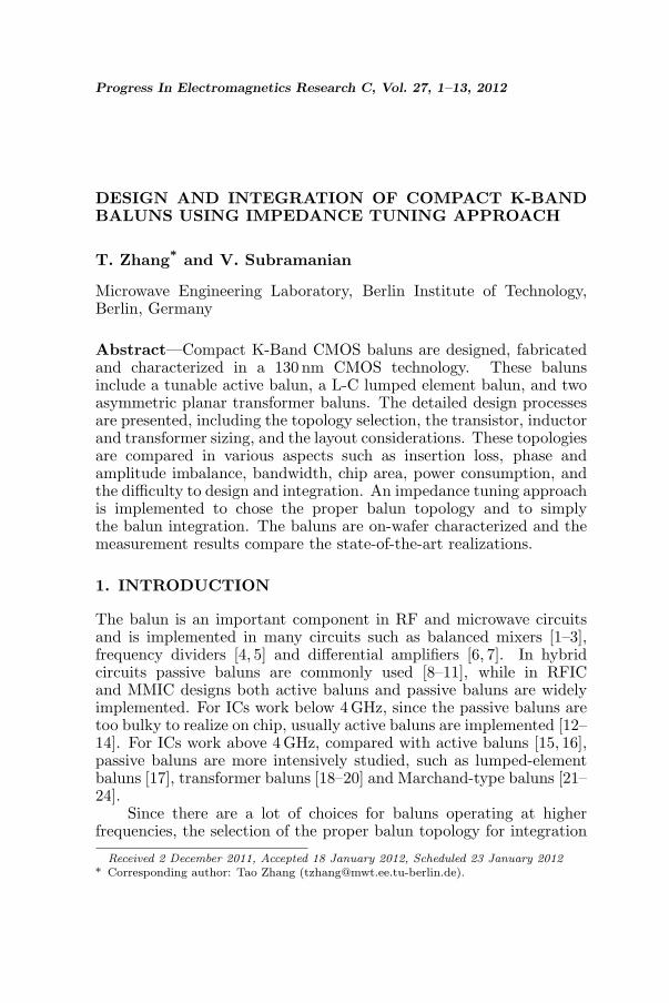
Figure 2 shows the simulated amplitude and phase imbalanceversus C1 and C3 capacitance. The simulation frequency is 24 GHz.The default capacitances of C1 ∼ C3 are 0.1 pF, 0.3 pF, 0.06 pF,respectively. The Q-factors of the varactors are set to 5. It can beseen that C3 has a large influence on ∆φ and C1 has a large influenceon ∆A. By changing the biasing voltage of the varactors, ∆A variesby ±2 dB and ∆φ varies by ±10 degree.
2.2. Lumped-element Balun
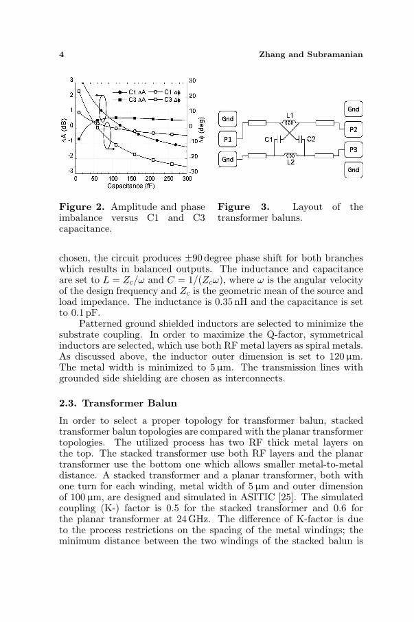
The lattice-type L-C balun shown in Figure 3 consists of two capacitorsand inductors. When the inductor and capacitor values are carefully
4 Zhang and Subramanian
Figure 2. Amplitude and phaseimbalance versus C1 and C3capacitance.
Figure 3. Layout of thetransformer baluns.
chosen, the circuit produces ±90 degree phase shift for both brancheswhich results in balanced outputs. The inductance and capacitanceare set to L = Zc/ω and C = 1/(Zcω), where ω is the angular velocityof the design frequency and Zc is the geometric mean of the source andload impedance. The inductance is 0.35 nH and the capacitance is setto 0.1 pF.
Patterned ground shielded inductors are selected to minimize thesubstrate coupling. In order to maximize the Q-factor, symmetricalinductors are selected, which use both RF metal layers as spiral metals.As discussed above, the inductor outer dimension is set to 120µm.The metal width is minimized to 5µm. The transmission lines withgrounded side shielding are chosen as interconnects.
2.3. Transformer Balun
In order to select a proper topology for transformer balun, stackedtransformer balun topologies are compared with the planar transformertopologies. The utilized process has two RF thick metal layers onthe top. The stacked transformer use both RF layers and the planartransformer use the bottom one which allows smaller metal-to-metaldistance. A stacked transformer and a planar transformer, both withone turn for each winding, metal width of 5µm and outer dimensionof 100 µm, are designed and simulated in ASITIC [25]. The simulatedcoupling (K-) factor is 0.5 for the stacked transformer and 0.6 forthe planar transformer at 24 GHz. The difference of K-factor is dueto the process restrictions on the spacing of the metal windings; theminimum distance between the two windings of the stacked balun is
Progress In Electromagnetics Research C, Vol. 27, 2012 5
4µm, while for the planar balun is only 2µm. Because the planartransformer balun has larger K-factor than the stacked transformerbalun under constant Q-factor of the windings in both the cases, itcan be mentioned that the planar balun has smaller IL. EM simulationusing ADS Momentum shows that the planar balun has 0.15 dB highergain than the stacked balun at 24 GHz.
In order to design the planar transformer baluns, the outerdimension and number of turns should be optimized first. The peakQ frequency of the windings should be at K-Band. Figure 4 showsthe peak Q frequency of the inductors versus the outer dimensionand number of turns. The inductors are rectangular planar inductorswith 5µm metal width. If the inductor outer dimension is between100µm and 120µm, and the number of turns is between 1 and 2, the
Figure 4. Inductor peak Q frequency versus the outer dimension andnumber of turns.
(a) (b)
Figure 5. Layout of the transformer baluns.
6 Zhang and Subramanian
peak frequency is near K-Band. The number of turns in the primarywinding is selected as 2, while in the secondary winding is 1.5. Theouter dimension of the balun is 100µm.
The layout of the two transformer baluns is shown in Figure 5.These two baluns is designed differently to integrate with differentcircuits. The patterned bottom metal acts as ground shielding. Theimplementation of patterned ground avoids the eddy current loss in thesubstrate and ensures high Q-factor of the windings. The input portP1 is matched to 50 Ω at 24 GHz by adding a 0.1 pF series capacitor.The balun outer dimension is slightly modified to tune the windinginductance and improve the input matching. The output ports arenot connected with capacitors since by simulation a series capacitorincreases the IL. The return loss of P2 and P3 are −5 dB with 50Ωload impedance at 24 GHz.
The transformer topology ensures the phase balance [18], but theamplitude balance is still a problem. To solve this problem, the positionof the center-tap on the secondary winding is moved along the winding.By moving the center-tap position, the coupling of the primary windingwith one branch of the secondary winding increases, while the couplingwith the other branch decreases and hence the amplitude imbalancecould be compensated. It should be notice that the phase imbalancealso slightly alters.
2.4. Topology Comparison
Table 1 compares the performances of the three balun topologies. Theadvantages and disadvantages of all topologies are illustrated in thistable. The active balun is good for their gain and wide bandwidth, butsuffers from chip size and linearity. The lumped-element balun is goodfor their low loss and easy to design, the disadvantage is their narrowbandwidth. Although the lumped-element balun might be improvedto overcome the narrow bandwidth, the chip size also becomes largersince more inductors will be implemented. The transformer baluns isthe best choice for most cases for the wide bandwidth, small chip sizeand simplicity to integration.
Table 1. Comparison of the balun topologies at K-band.
Topology IL B.W. Chip Size Design Integration
Active With Gain Wide Large Normal Normal
L-C Low Narrow Large Easy Normal
Transformer Medium Wide Small Normal Easy
Progress In Electromagnetics Research C, Vol. 27, 2012 7
(a) (b)
(c) (d)
Figure 6. Load impedance tuning for (a) active balun; (b) L-C balun;(c) transformer balun T1; (d) transformer balun T2.
3. IMPEDANCE TUNING APPROACH
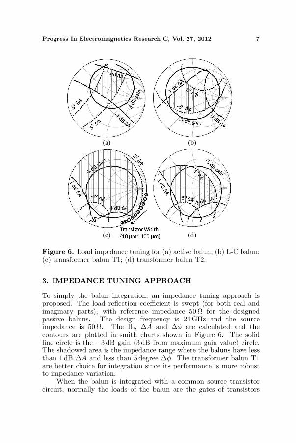
To simply the balun integration, an impedance tuning approach isproposed. The load reflection coefficient is swept (for both real andimaginary parts), with reference impedance 50 Ω for the designedpassive baluns. The design frequency is 24 GHz and the sourceimpedance is 50 Ω. The IL, ∆A and ∆φ are calculated and thecontours are plotted in smith charts shown in Figure 6. The solidline circle is the −3 dB gain (3 dB from maximum gain value) circle.The shadowed area is the impedance range where the baluns have lessthan 1 dB ∆A and less than 5 degree ∆φ. The transformer balun T1are better choice for integration since its performance is more robustto impedance variation.
When the balun is integrated with a common source transistorcircuit, normally the loads of the balun are the gates of transistors
8 Zhang and Subramanian
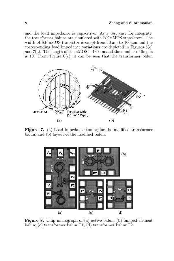
and the load impedance is capacitive. As a test case for integrate,the transformer baluns are simulated with RF nMOS transistors. Thewidth of RF nMOS transistor is swept from 10µm to 100µm and thecorresponding load impedance variations are depicted in Figures 6(c)and 7(a). The length of the nMOS is 130 nm and the number of fingersis 10. From Figure 6(c), it can be seen that the transformer balun
(a) (b)
Figure 7. (a) Load impedance tuning for the modified transformerbalun; and (b) layout of the modified balun.
(a)
(b)
(c) (d)
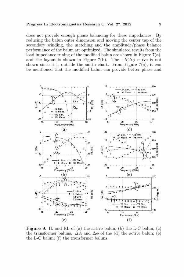
Figure 8. Chip micrograph of (a) active balun; (b) lumped-elementbalun; (c) transformer balun T1; (d) transformer balun T2.
Progress In Electromagnetics Research C, Vol. 27, 2012 9
does not provide enough phase balancing for these impedances. Byreducing the balun outer dimension and moving the center tap of thesecondary winding, the matching and the amplitude/phase balanceperformance of the balun are optimized. The simulated results from theload impedance tuning of the modified balun are shown in Figure 7(a),and the layout is shown in Figure 7(b). The +5∆φ curve is notshown since it is outside the smith chart. From Figure 7(a), it canbe mentioned that the modified balun can provide better phase and
(a)
(b)
(c)
(d)
(e)
(f)
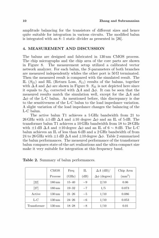
Figure 9. IL and RL of (a) the active balun; (b) the L-C balun; (c)the transformer baluns. ∆A and ∆φ of the (d) the active balun; (e)the L-C balun; (f) the transformer baluns.
10 Zhang and Subramanian
amplitude balancing for the transistors of different sizes and hencequite suitable for integration in various circuits. The modified balunis integrated with an 8 : 1 static divider as presented in [26].
4. MEASUREMENT AND DISCUSSION
The baluns are designed and fabricated in 130 nm CMOS process.The chip micrographs and the chip area of the core parts are shownin Figure 8. The measurement setup utilized a calibrated vectornetwork analyzer. For each balun, the S-parameters of both branchesare measured independently whiles the other port is 50 Ω terminated.Then the measured result is compared with the simulated result. TheIL (S21) and RL (Return Loss, S11) results of the baluns, togetherwith ∆A and ∆φ are shown in Figure 9. S31 is not depicted here sinceit equals to S21 corrected with ∆A and ∆φ. It can be seen that themeasured results match the simulation well, except for the ∆A and∆φ of the L-C balun. As mentioned before, this discrepancy is dueto the sensitiveness of the L-C balun to the load impedance variation.A slight variation of the load impedance changes the balancing of theL-C balun.
The active balun T1 achieves a 5 GHz bandwidth from 21 to26GHz with ±1 dB ∆A and ±10 degree ∆φ and an IL of 5 dB. Thetransformer balun T1 achieves a 10 GHz bandwidth from 18 to 28 GHzwith ±1 dB ∆A and ±10 degree ∆φ and an IL of 6 ∼ 8 dB. The L-Cbalun achieves an IL of less than 6 dB and a 2 GHz bandwidth of from24 to 26GHz with ±1 dB ∆A and ±10 degree ∆φ. Table 2 summarizedthe balun performances. The measured performance of the transformerbalun compares state-of-the-art realizations and the ultra-compact sizemake it very suitable for integration at this frequency band.
Table 2. Summary of balun performances.
CMOS
Process
Freq
(GHz)
IL
(dB)
∆A (dB)/
∆φ (degree)
Chip Area
(mm2)
[22] 180 nm 15–40 −9 2/10 0.06
[27] 180 nm 19–32 −7 1/5 0.073
Active 130 nm 21–26 −5 1/10 0.086
L-C 130 nm 24–26 −6 1/10 0.053
Transformer 130 nm 18–28 −8 1/10 0.01
Progress In Electromagnetics Research C, Vol. 27, 2012 11
5. CONCLUSION
Three balun topologies, active balun, lumped element balun andtransformer balun are compared for CMOS K-Band applications. It isfound that the active balun is a suitable choice when the balun requiresa high gain, while the transformer balun is the right choice when thebalun needs to be broadband and miniature. The impedance tuningmethod is implemented to characterize the balun performance and tosimplify the integration. The measurement results show that designedbalun compares with the state of the art realizations in K-Band.
ACKNOWLEDGMENT
This work is part of the LOWILO project (BMBF ProjectNo. 16SV3654). The authors wish to acknowledge BMBF forsponsoring and other project partners for their support.
REFERENCES
1. Rao, P. Z., T. Y. Chang, C. P. Liang, and S. J. Chung, “An ultra-wideband high-linearity CMOS mixer with new wideband activebaluns,” IEEE Microw. Theory Tech., Vol. 57, No. 9, 2184–2192,2009.
2. Wei, C. C., H. C. Chiu, H. C. Hsu, W. S. Feng, and J. S. Fu, “Fullyintegrated 24 GHz differential active sub-harmonic mixer locatedin CMOS multi-layer Marchand baluns,” IET Microw. AntennaProp., Vol. 4, No. 11, 1789–1798, 2010.
3. Jeong, J. C., I. B. Yom, and K. W. Yeom, “An active IF balun for adoubly balanced resistive mixer,” IEEE Microw. Wirel. Compon.Lett., Vol. 19, No. 4, 224–226, 2009.
4. Trotta, S., H. Li, V. P. Trivedi, and J. John, “A tunable flipflop-based frequency divider up to 113GHz and a fully differential77GHz push-push VCO in SiGe BiCMOS technology,” IEEERFIC Symposium 2009 , 47–50, 2009.
5. Chen, H. K., H. J. Chen, D. C. Chang, Y. Z. Juang, Y. C. Yang,and S. S. Lu, “A mm-wave CMOS multimode frequency divider,”IEEE ISSCC 2009 , 280–281, 2009.
6. Afsahi, A., A. Behzad, V. Magoon, and L. E. Larson, “Fullyintegrated dual-band power amplifiers with on-chip baluns in65 nm CMOS for an 802.11n MIMO WLAN SoC,” IEEE RFICSymposium 2009 , 365–368, 2009.
12 Zhang and Subramanian
7. Kidwai, A. A., A. Nazimov, Y. Eilat, and O. Degani, “Fullyintegrated 23 dBm transmit chain with on-chip power amplifierand balun for 802.11a application in standard 45 nm CMOSprocess,” IEEE RFIC Symposium 2009 , 273–276, 2009.
8. Lin, C.-M., C.-C. Su, S.-H. Hung, and Y.-H. Wang, “A compactbalun based on microstrip EBG cell and interdigital capacitor,”Progress In Electromagnetics Research Letters, Vol. 12, 111–118,2009.
9. Yeh, Z.-Y. and Y.-C. Chiang, “A miniature CPW balunconstructed with length-reduced 3 dB couples and a shortredundant transmission line,” Progress In ElectromagneticsResearch, Vol. 117, 195–208, 2011.
10. Persico, R., N. Romano, and F. Soldovieri, “Design of a balunfor a bow tie antenna in reconfigurable ground penetrating radarsystems,” Progress In Electromagnetics Research C , Vol. 18, 123–135, 2011.
11. Shao, J., H. C. Zhang, C. Chen, S. Tan, and K. J. Chen, “Acompact dual-band coupled-line balun with tapped open-endedstubs,” Progress In Electromagnetics Research C , Vol. 22, 109–122, 2011.
12. Ji, Y., C. Wang, J. Liu, and H. Liao, “1.8 dB NF 3.6 mW CMOSactive balun low noise amplifier for GPS,” Electronics Letters,Vol. 46, No. 3, 251–252, 2010.
13. Mastantuono, D. and D. Manstretta, “A low-noise active balunwith IM2 cancellation for multiband portable DVB-H receivers,”IEEE ISSCC 2009 , 216–217, 2009.
14. Godara, B. and A. Fabre, “A highly compact active widebandbalun with impedance transformation in SiGe BiCMOS,” IEEEMicrow. Theory Tech., Vol. 56, No. 1, 22–30, 2008.
15. Jung, K., W. R. Eisenstadt, R. M. Fox, A. W. Ogden, andJ. Yoon, “Broadband active balun using combined cascode-cascade configuration,” IEEE Microw. Theory Tech., Vol. 56,No. 8, 1790–1796, 2008.
16. Huang, B. J., B. J. Huang, K. Y. Lin, and H. Wang, “A 2–40 GHzactive balun using 0.13µm CMOS process,” IEEE Microw. Wirel.Compon. Lett., Vol. 19, No. 3, 164–166, 2009.
17. Chiou, H. K., H. H. Lin, and C. Y. Chang, “Lumped-elementcompensated high/low-pass balun design for MMIC double-balanced mixer,” IEEE Microw. and Guided Wave Letters, Vol. 7,No. 8, 248–250, 1997.
Progress In Electromagnetics Research C, Vol. 27, 2012 13
18. Long, J. R., “Monolithic transformers for silicon RF IC design,”IEEE J. Solid-State Circuits, Vol. 35, No. 9, 1368–1382, 2000.
19. Hsu, H. M., J. S. Huang, S. Y. Chen, and S. H. Lai, “Design ofan on-chip balun with a minimum amplitude imbalance using asymmetric stack layout,” IEEE Microw. Theory Tech., Vol. 58,No. 4, 814–819, 2010.
20. Chiou, H. K. and T. Y. Yang, “Low-loss and broadbandasymmetric broadside-coupled balun for mixer design in 0.18µmCMOS technology,” IEEE Microw. Theory Tech., Vol. 56, No. 4,835–848, 2008.
21. Huang, C. H., C. H. Chen, and T. S. Horng, “Design of integratedplanar Marchand balun using physical transformer model,” AsiaPacific Microw. Conf. 2009 , 1004–1007, 2009.
22. Chiang, M. J., H. S. Wu, and C. K. C. Tzuang, “A compactCMOS Marchand balun incorporating meandered multilayer edge-coupled transmission lines,” Microwave Symposium Digest 2009 ,125–128, 2009.
23. Yang, Z. Q., T. Yang, and Y. Liu, “Analysis and design of areduced-size marchand balun,” Journal of Electromagnetic Wavesand Applications, Vol. 21, No. 9, 1169–1175, 2007.
24. Ercoli, M., M. Kraemer, D. Dragomirescu, and R. Plana, “Anultra small passive balun for 60 GHz applications in CMOS 65 nmtechnology,” NEWCAS Conference 2010 , 329–332, 2010.
25. Niknejad, A. M., “Modeling of passive elements with ASITIC,”Microwave Symposium Digest 2002 , 149–152, 2002.
26. Shu, R., V. Subramanian, and G. Boeck, “Millimeter-wavestatic frequency divider in 0.13-m CMOS technology,” NEWCASConference 2011 , 2011.
27. Yu, H. Y., S. S. Choi, S. H. Kim, and Y. H. Kim, “K-Band balunwith slot pattern ground for wide operation using 0.18µm CMOStechnology,” Electronics Letters, Vol. 43, No. 5, 51–52, 2007.