Page 1
i
Design and Modeling of I2C Bus Controller A Thesis Submitted in Partial Fulfillment of the Requirements
for the Master of Technology
By
Debasis Behera
Regd No:209ec2121
VLSI Design & Embedded System
Under the supervision
of
Prof. D.P.Acharya
Department of Electronics & Communication Engineering
National Institute of Technology, Rourkela
Rourkela – 769008
May-2011
Page 2
ii
DedicatedDedicatedDedicatedDedicated
TTTToooo
MMMMyyyy ParentsParentsParentsParents
Page 3
iii
ACKNOWLEDGEMENT
I would like to thank my mentor Prof. D.P. Acharya for his constant
support, encouragement, and valuable guidance throughout this project.
I express my deep gratitude to Prof. S.K. Patra (HOD, Department of
Electronics & Communication Engineering) and Prof. K.K. Mahapatra for their
active coordination and support to complete the project.
I would also like to thank my senior fellow researchers in the VLSI
Design Lab, especially Mr. Ayaskanta Swain.
Finally, I would like to extend my appreciation to my family members
and my friends who are always beside me and help me in the most difficult
times inside or outside the laboratory.
Page 4
iv
ABSTRACT This thesis is concerned with the design of I2C bus controller and the interface between the
I2C devices i.e. microcontroller (AT89C51) and EEPROM (AT24C16). The I2C is a two wire
serial protocol. Hence I2C components can be interfaced by using only two lines. First one is
serial data (SDA) line and second is serial clock (SCL) line. The design architecture consists
of a master controller and a slave. The master generates the START condition when SCL is
HIGH and SDA is having a transition from HIGH to LOW. Master also generates STOP
condition when SCL is in HIGH and SDA is having a transition from LOW to HIGH. Beside
these two functions master also transfers and receives data to/from different slave devices.
When master transmits data to slave receiver then it is known as WRITE mode of operation
and when master receives data from slave transmitter then it is known as READ mode of
operation. The microcontroller and EEPROM are interfaced through I2C bus. Data send, read
and write particularly these operations are carried out and the behavior of I2C protocol is
examined. In later section the I2C master controller is designed in verilg HDL. By describing
the design in HDL, functional verification of the design can be done early in the design cycle.
Since designers work at the high level language, they can optimize and modify the design
module until it meets the desired functionality. The test bench program has to be developed
to test the design module. The test bench gives the input to the design module & verifies the
outputs. The test bench has to be written in such way to check the design module in all
possible conditions.
Page 5
v
Contents
ACKNOWLEDGEMENT ................................................................................................................ iii
ABSTRACT .................................................................................................................................... iv
LIST OF FIGURES ........................................................................................................................ vii
LIST OF TABLES ......................................................................................................................... viii
CHAPTER-1 ..................................................................................................................................... 1
INTRODUCTION ............................................................................................................................ 1
1.1 Object and Scope of Thesis: ..................................................................................................... 2
1.2 Need for I2C Bus: .................................................................................................................... 2
CHAPTER-2 ..................................................................................................................................... 3
OVERVIEW OF I2C BUS PROTOCOL ............................................................................................ 3
2.1 Introduction to I2C Bus Protocol System: ................................................................................. 4
2.2 I2C Bus Terminology: .............................................................................................................. 4
2.3 Master and Slave: .................................................................................................................... 5
2.4 Data Validity: .......................................................................................................................... 6
2.5 START and STOP condition: .................................................................................................. 6
2.6 Byte format Data Transfer: ...................................................................................................... 7
2.7 Device Addressing: ................................................................................................................. 8
2.8 Acknowledge (ACK) and Not Acknowledge (NACK) ............................................................. 8
2.9 Read and write operation: ........................................................................................................ 9
2.9.1 Write operation: .............................................................................................................. 10
2.9.2 Read operation: ............................................................................................................... 10
2.10 Clock synchronization: ........................................................................................................ 11
2.11 Arbitration ........................................................................................................................... 12
2.12 Summary ............................................................................................................................. 13
CHAPTER-3 ................................................................................................................................... 14
INTERFACING SERIAL EEPROM (AT24C16) WITH 8051 MICROCONTROLLER (AT89C51) USING I2C BUS ............................................................................................................................. 14
3.1 Introduction: .......................................................................................................................... 15
3.2 I2C Experimental Board: ........................................................................................................ 15
3.3 AT24C16 Pin configuration: .................................................................................................. 16
Page 6
vi
3.4 Device Addressing: ............................................................................................................... 17
3.5 Start condition: ...................................................................................................................... 18
3.6 Transfer a bit of a word to/from EEPROM: ............................................................................ 18
3.7 Transfer of a word to/from EEPROM: ................................................................................... 19
3.8 Monitoring Acknowledgement bit: ........................................................................................ 20
3.9 Read/write operation:............................................................................................................. 20
3.10 Stop condition: .................................................................................................................... 20
3.11 Memory addressing: ............................................................................................................ 21
3.12 Clocking: ............................................................................................................................. 21
3.13 Byte write operation: ........................................................................................................... 21
3.14 Random read operation: ....................................................................................................... 22
3.15 KEIL Micro vision Logic Analyzer output: .......................................................................... 23
3.16 Summary: ............................................................................................................................ 24
CHAPTER-4 ................................................................................................................................... 25
I2C BUS CONTROLLER DESIGN ................................................................................................. 25
4.1 Introduction: .......................................................................................................................... 26
4.2 I2C Protocol: .......................................................................................................................... 26
4.3 Design steps: ......................................................................................................................... 27
4.4 Design Goals and Limitation: ................................................................................................ 27
4.5 I2C Bus Architecture: ............................................................................................................. 28
4.6 Top-Level Signal Descriptions: .............................................................................................. 28
4.7 Register Definitions: .............................................................................................................. 30
4.8 Flowchart: ............................................................................................................................. 31
4.8 Simulation Results: ................................................................................................................ 31
4.9 Summary: .............................................................................................................................. 37
CHAPTER- 5 .................................................................................................................................. 38
CONCLUSION AND SUGGESTS FUTURE WORK ..................................................................... 38
5.1 Conclusion: ........................................................................................................................... 39
5.2 Future work: .......................................................................................................................... 39
References: ................................................................................................................................. 40
Page 7
vii
LIST OF FIGURES Figure2.1 I2C bus configuration using masters and slaves .................................................................. 4
Figure2.2 Data validity condition ...................................................................................................... 6
Figure2.3 Start and stop condition ..................................................................................................... 7
Figure2.4 Data transfer on the I2C bus ............................................................................................... 7
Figure2.5 Slave address ..................................................................................................................... 8
Figure2.6 Acknowledgement of I2C bus ............................................................................................ 9
Figure2.7 Master transmits to slave receiver (WRITE) mode ........................................................... 10
Figure2.8 Master read after setting the word address (READ) mode ................................................ 11
Figure3.1 Architecture of AT89C51 microcontroller and AT24C16 EEPROM Interfacing............... 16
Figure3.2 Device addressing of 24C16 ............................................................................................ 17
Figure3.3 EEPROM start condition ................................................................................................. 18
Figure3.4 Transfer a bit of a word to/from EEPROM....................................................................... 19
Figure3.5 Transfer of a word to/from EEPROM .............................................................................. 19
Figure3.6 Read/write operation of EEPROM ................................................................................... 20
Figure3.7 Stop condition of EEPROM ............................................................................................. 20
Figure3.8 Memory addressing of EEPROM..................................................................................... 21
Figure3.9 Clocking condition .......................................................................................................... 21
Figure3.10 START & Single write byte ........................................................................................... 23
Figure3.11 STOP & Single read byte ............................................................................................... 23
Figure3.12 After read (FF) .............................................................................................................. 24
Figure4.1 I2C master controller pin level architecture ...................................................................... 28
Figure4.2 Communication application flowchart ............................................................................. 31
Figure4.3 START condition ............................................................................................................ 31
Figure4.4 Master transmits to slave receiver (WRITE). ................................................................... 32
Figure4.5 Master transmits to slave receiver (WRITE). ................................................................... 32
Figure4.6 Acknowledgement condition ........................................................................................... 33
Figure4.7 Master transmits to slave receiver (WRITE). ................................................................... 33
Figure4.8 Master transmits to slave receiver (WRITE). ................................................................... 34
Figure4.9 Repeated start condition .................................................................................................. 34
Figure4.10 Master reads slave (READ) ........................................................................................... 35
Figure4.11 Master reads slave (READ) ........................................................................................... 35
Figure4.12 Master reads slave (READ) ........................................................................................... 36
Figure4.13 Master reads slave (READ) ........................................................................................... 36
Figure4.14 STOP condition ............................................................................................................. 37
Page 8
viii
LIST OF TABLES Table4.1 Signal Description of I2C Master Controller ...................................................................... 29
Table4.2 Register Description of I2C Master Controller ................................................................... 30
Page 9
1
CHAPTER-1
INTRODUCTION
Page 10
2
1.1 Object and Scope of Thesis: The object of this thesis is to design an I2C bus protocol controller by using verilog
HDL language and match the waveform or output generated by the software Questasim
(Questa 64 6.5b) with our desired I2C bus controller output. Specifically, this thesis
describes in detail an I2C Master connected to I 2C Slave using an I2C bus. The I2C Master
can be a Microcontroller (89C51). The Microcontroller board in turn is connected to a host
computer by a RS232 link. Finally, software (keil microvision) running on the host computer,
which is capable of establishing a serial port connection and drawing waveforms based on
received data, will be discussed. The I2C Interface is operating in 7-bit address mode,
meaning one master is able to manage 27 or 128 slaves.
There are five chapters in this thesis. In Chapter 2, I will discuss the I2C bus protocol to
provide readers a basic knowledge of the I2C bus. In Chapter 3, a prototype system for fully
testing the I2C Interface is described. The prototype system includes one Slave (EEPROM)
with its address and a Master, a serial communication link (RS232) between the Master and a
host computer, and software running on the host computer for display purposes. Chapter 4,
describes, in detail, the design of the I2C Master Controller using verilog HDL and how it
behaves after running in the software. Finally, Chapter 5 provides a conclusion and suggests
possible future work.
1.2 Need for I2C Bus: The on-chip RAM (EEPROM), Oscillator (RTC), ADC and I2C Interface will be
integrated for the purpose to Communicate between them. The presence of a RTC and an on-
chip RAM introduces an immediate need for a data communication between the chip and a
host computer to send data on the RAM. To minimize the system-level interconnect, I
propose to transmit the contents of the RAM storing the results back to a host computer via a
serial bus, the I2C Interface. This greatly simplifies the system level design and in particular
the design of the mother-board and associated chip-boards. Moreover, storing data in a
digital format on-chip before transmittal to a host computer over the I2C Interface will result
in an improved system performance since the transmission of digital data is much less
susceptible to interference from environmental noise sources.
Page 11
3
CHAPTER-2
OVERVIEW OF I 2C BUS PROTOCOL
Page 12
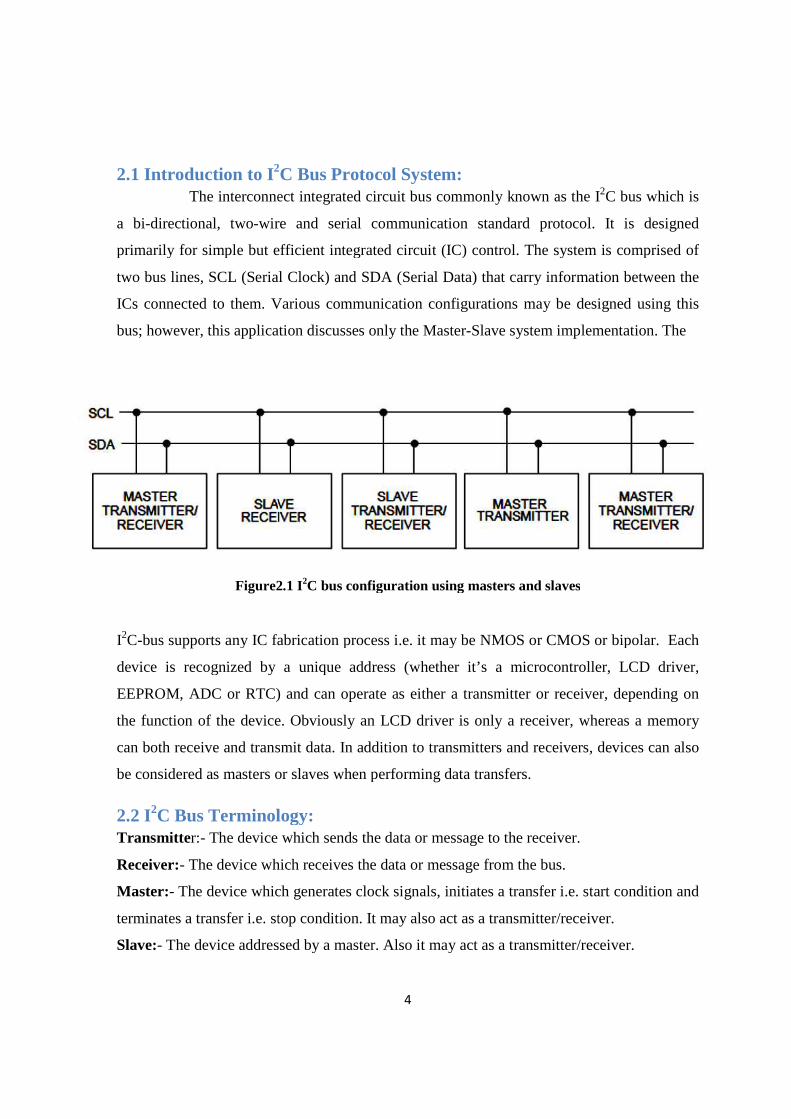
2.1 Introduction to I2
The interconnect
a bi-directional, two-wire
primarily for simple but efficient integrated circuit (IC) control. The system is comprised of
two bus lines, SCL (Serial Clock) and
ICs connected to them. Various communication configurations may be designed using this
bus; however, this application
Figure2
I2C-bus supports any IC fabrication process i.e. it may be NMOS or CMOS or bip
device is recognized by a unique address (whether it’s a microcontroller, LCD driv
EEPROM, ADC or RTC) and can
the function of the device. Obviously an LCD driver is only a receiver, whereas a memory
can both receive and transmit data. In addition to transmitters and receivers, devices can also
be considered as masters or slaves when perform
2.2 I2C Bus Terminology:Transmitter:- The device w
Receiver:- The device which receives the data or message from the bus.
Master:- The device which
terminates a transfer i.e. stop condition. It may also act as a transmitter/receiver.
Slave:- The device addressed by a master. Also it may act as a transmitter/receiver.
4
2C Bus Protocol System: nterconnect integrated circuit bus commonly known as
wire and serial communication standard protocol
primarily for simple but efficient integrated circuit (IC) control. The system is comprised of
two bus lines, SCL (Serial Clock) and SDA (Serial Data) that carry information between the
ICs connected to them. Various communication configurations may be designed using this
application discusses only the Master-Slave system implementation
2.1 I2C bus configuration using masters and slaves
ny IC fabrication process i.e. it may be NMOS or CMOS or bip
device is recognized by a unique address (whether it’s a microcontroller, LCD driv
) and can operate as either a transmitter or receiver, depending on
the function of the device. Obviously an LCD driver is only a receiver, whereas a memory
can both receive and transmit data. In addition to transmitters and receivers, devices can also
as masters or slaves when performing data transfers.
erminology: The device which sends the data or message to the receiver.
hich receives the data or message from the bus.
The device which generates clock signals, initiates a transfer i.e. start condition and
terminates a transfer i.e. stop condition. It may also act as a transmitter/receiver.
The device addressed by a master. Also it may act as a transmitter/receiver.
us commonly known as the I2C bus which is
rotocol. It is designed
primarily for simple but efficient integrated circuit (IC) control. The system is comprised of
) that carry information between the
ICs connected to them. Various communication configurations may be designed using this
Slave system implementation. The
C bus configuration using masters and slaves
ny IC fabrication process i.e. it may be NMOS or CMOS or bipolar. Each
device is recognized by a unique address (whether it’s a microcontroller, LCD driver,
operate as either a transmitter or receiver, depending on
the function of the device. Obviously an LCD driver is only a receiver, whereas a memory
can both receive and transmit data. In addition to transmitters and receivers, devices can also
hich sends the data or message to the receiver.
hich receives the data or message from the bus.
generates clock signals, initiates a transfer i.e. start condition and
terminates a transfer i.e. stop condition. It may also act as a transmitter/receiver.
The device addressed by a master. Also it may act as a transmitter/receiver.
Page 13
5
Multi master: - More than one master can attempt control the bus at the same time without
demeaning the data/message.
Arbitration: - It is a procedure to ensure that, if more than one master simultaneously tries to
control the bus, only one is allowed to do so and the data is not corrupted.
Synchronization:- It is a procedure to synchronize the clock signals of two or more devices.
2.3 Master and Slave: A master is the device which initiates a data transfer on the bus and generates the
clock signals to permit that transfer. At that time, any device addressed is considered a slave.
Both lines are connected to a positive supply via a pull-up resistor, and remain HIGH when
the bus is not busy. Each device is recognized by a unique address—whether it is a
microcomputer, LCD driver, memory or keyboard interface—and can operate as either a
transmitter or receiver, depending on the function of the device. A device generating a
message or data is a transmitter, and a device receiving the message or data is a receiver.
Obviously, a passive function like an LCD driver could only be a receiver, while a
microcontroller or a memory can both transmit and receive data. When a data transfer takes
place on the bus, a device can either be a master or a slave. The device which initiates the
transfer, and generates the clock signals for this transfer, is the master. At that time any
device addressed is considered a slave. It is important to note that a master could either be a
transmitter or a receiver; a master microcontroller may send data to a RAM acting as a
transmitter, and then interrogate the RAM for its contents acting as a receiver in both cases
performing as the master initiating the transfer. In the same manner, a slave could be both a
receiver and a transmitter. The I2C is a multimaster bus. It is possible to have, in one system,
more than one device capable of initiating transfers and controlling the bus. A
microcontroller may act as a master for one transfer, and then be the slave for another
transfer, initiated by another processor on the network. The master/slave relationships on the
bus are not permanent, and may change on each transfer.
As more than one master may be connected to the bus, it is possible that two
devices will try to initiate a transfer at the same time. Obviously, in order to eliminate bus
collisions and communications chaos, an arbitration procedure is necessary. The I2C design
has an inherent arbitration and clock synchronization procedure relying on the wired-AND
Page 14
connection of the devices on the bus. In a typical multimaster system, a microcontroller
program should allow it to gracefully switch between master and slave modes and preserve
data integrity upon loss of arbitration.
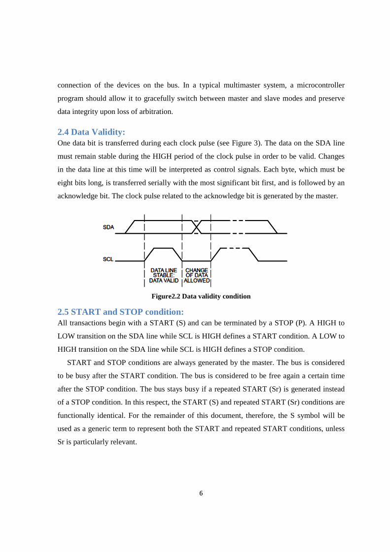
2.4 Data Validity: One data bit is transferred
must remain stable during the HIGH period of the clock pulse in order to be valid. Changes
in the data line at this time will be interpreted a
eight bits long, is transferred serially with the most significant bit first, and is followed by an
acknowledge bit. The clock pulse related to the acknowledge bit is generated by the mas
2.5 START and STOP conditionAll transactions begin with a START (S) and can be terminated by a STOP (P). A HIGH to
LOW transition on the SDA line while SCL is HIGH defines a START condition. A LOW to
HIGH transition on the SDA line while SCL is HIGH defines
START and STOP conditions are always generated by the master. The bus is considered
to be busy after the START condition. The bus is considered to be free again a certain time
after the STOP condition. The bus stays busy if a repeate
of a STOP condition. In this respect, the START (S) and repeated START (Sr) conditions are
functionally identical. For the remainder of this document, therefore, the S symbol will be
used as a generic term to represent bot
Sr is particularly relevant.
6
f the devices on the bus. In a typical multimaster system, a microcontroller
program should allow it to gracefully switch between master and slave modes and preserve
rity upon loss of arbitration.
One data bit is transferred during each clock pulse (see Figure 3). The data on the SDA line
must remain stable during the HIGH period of the clock pulse in order to be valid. Changes
in the data line at this time will be interpreted as control signals. Each byte, which must be
bits long, is transferred serially with the most significant bit first, and is followed by an
. The clock pulse related to the acknowledge bit is generated by the mas
Figure2.2 Data validity condition
START and STOP condition: All transactions begin with a START (S) and can be terminated by a STOP (P). A HIGH to
LOW transition on the SDA line while SCL is HIGH defines a START condition. A LOW to
HIGH transition on the SDA line while SCL is HIGH defines a STOP condition.
START and STOP conditions are always generated by the master. The bus is considered
to be busy after the START condition. The bus is considered to be free again a certain time
after the STOP condition. The bus stays busy if a repeated START (Sr) is generated instead
of a STOP condition. In this respect, the START (S) and repeated START (Sr) conditions are
functionally identical. For the remainder of this document, therefore, the S symbol will be
used as a generic term to represent both the START and repeated START conditions, unless
f the devices on the bus. In a typical multimaster system, a microcontroller
program should allow it to gracefully switch between master and slave modes and preserve
during each clock pulse (see Figure 3). The data on the SDA line
must remain stable during the HIGH period of the clock pulse in order to be valid. Changes
. Each byte, which must be
bits long, is transferred serially with the most significant bit first, and is followed by an
. The clock pulse related to the acknowledge bit is generated by the master.
All transactions begin with a START (S) and can be terminated by a STOP (P). A HIGH to
LOW transition on the SDA line while SCL is HIGH defines a START condition. A LOW to
a STOP condition.
START and STOP conditions are always generated by the master. The bus is considered
to be busy after the START condition. The bus is considered to be free again a certain time
d START (Sr) is generated instead
of a STOP condition. In this respect, the START (S) and repeated START (Sr) conditions are
functionally identical. For the remainder of this document, therefore, the S symbol will be
h the START and repeated START conditions, unless
Page 15
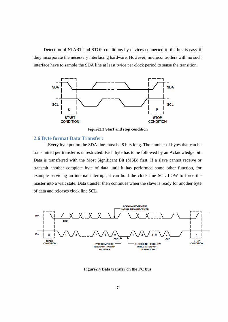
Detection of START and STOP conditions by devices connected to the bus is easy if
they incorporate the necessary interfacing hardware. However, microcontrollers with n
interface have to sample the SDA line at least twice per clock period to sense the transition.
2.6 Byte format Data Transfer Every byte put on the SDA line must be 8 bits
transmitted per transfer is unrestricted. Each byte has to be followed by an Acknowledge bit.
Data is transferred with the Most Significant Bit (MSB) first. If a slave cannot receive or
transmit another complete byte o
example servicing an internal interrupt, it can hold the clock line SCL LOW to force the
master into a wait state. Data transfer then continues when the slave is ready for another byte
of data and releases clock line SCL.
7
Detection of START and STOP conditions by devices connected to the bus is easy if
they incorporate the necessary interfacing hardware. However, microcontrollers with n
interface have to sample the SDA line at least twice per clock period to sense the transition.
Figure2.3 Start and stop condition
Byte format Data Transfer: Every byte put on the SDA line must be 8 bits long. The number of bytes that can be
transmitted per transfer is unrestricted. Each byte has to be followed by an Acknowledge bit.
Data is transferred with the Most Significant Bit (MSB) first. If a slave cannot receive or
transmit another complete byte of data until it has performed some other function, for
example servicing an internal interrupt, it can hold the clock line SCL LOW to force the
master into a wait state. Data transfer then continues when the slave is ready for another byte
ases clock line SCL.
Figure2.4 Data transfer on the I2C bus
Detection of START and STOP conditions by devices connected to the bus is easy if
they incorporate the necessary interfacing hardware. However, microcontrollers with no such
interface have to sample the SDA line at least twice per clock period to sense the transition.
long. The number of bytes that can be
transmitted per transfer is unrestricted. Each byte has to be followed by an Acknowledge bit.
Data is transferred with the Most Significant Bit (MSB) first. If a slave cannot receive or
f data until it has performed some other function, for
example servicing an internal interrupt, it can hold the clock line SCL LOW to force the
master into a wait state. Data transfer then continues when the slave is ready for another byte
Page 16
2.7 Device Addressing The addressing procedure for the I
condition usually determines which slave
The first seven bits of the first byte make up the slave address (see Fig.). The eighth
bit is the LSB (least significant bit). It determines the direction
the least significant position of the first byte means that the master will write information to a
selected slave. A ‘one’ in this position means that the master will read information from the
slave.
When an address is sent, each device in a system compares the first seven bits after the
START condition with its address. If they match, the device considers itself addressed by the
master as a slave-receiver or slave
A slave address can be ma
that there will be several identical devices in a system, the programmable part of the slave
address enables the maximum possible number of such devices to be connected to
bus. The number of programmable address bits of a device depends on the number of pins
available. For example, if a device has 4 fixed and 3 programmable address bits, a total of
identical devices can be connected to the same bus.
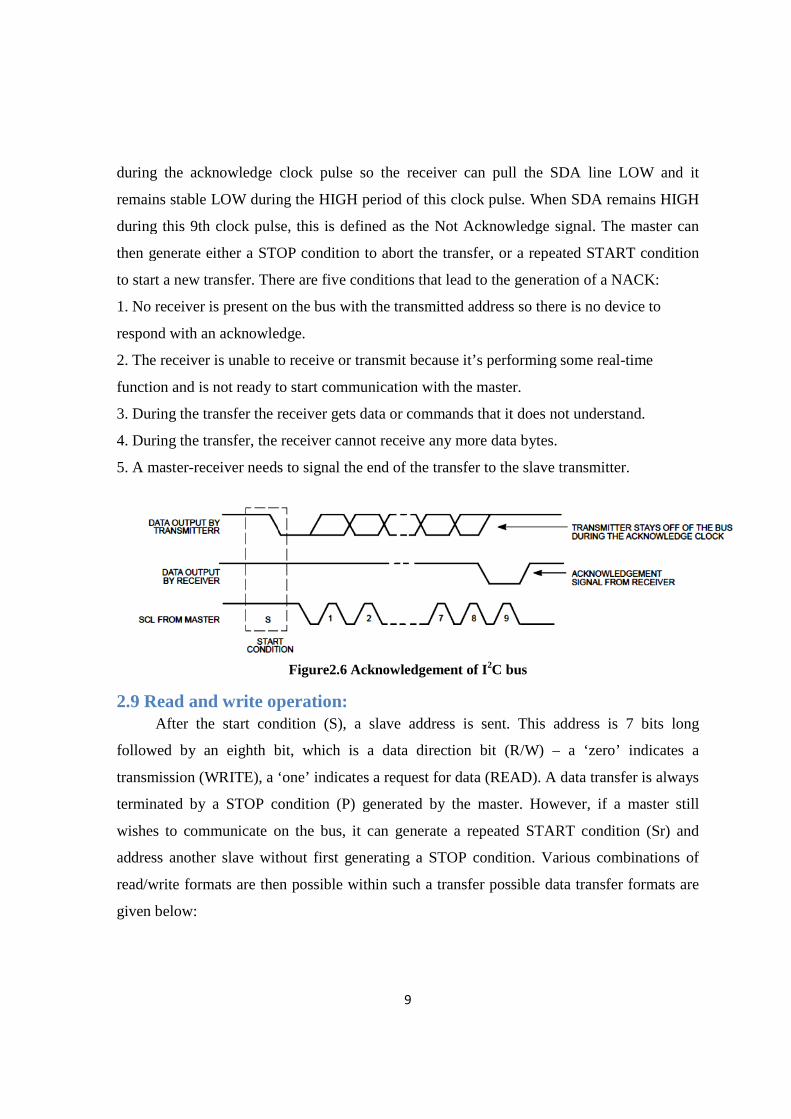
2.8 Acknowledge (ACK) and Not Acknowledge (NACK) The acknowledge takes place after every byte. The acknowledge bit allows the
receiver to signal the transmitter that the byte was successfully received and another byte
may be sent. All clock pulses including the acknowledge 9th clock pulse are generated b
master. The Acknowledge signal is defined as follows: the transmitter releases the SDA line
8
Device Addressing: The addressing procedure for the I2C bus is such that the first byte after the START
condition usually determines which slave will be selected by the master.
Figure2.5 Slave address
seven bits of the first byte make up the slave address (see Fig.). The eighth
bit is the LSB (least significant bit). It determines the direction of the message. A ’zero’ in
the least significant position of the first byte means that the master will write information to a
selected slave. A ‘one’ in this position means that the master will read information from the
s sent, each device in a system compares the first seven bits after the
START condition with its address. If they match, the device considers itself addressed by the
receiver or slave-transmitter, depending on the R/W bit.
slave address can be made-up of a fixed and a programmable part. Since it is likely
that there will be several identical devices in a system, the programmable part of the slave
address enables the maximum possible number of such devices to be connected to
bus. The number of programmable address bits of a device depends on the number of pins
available. For example, if a device has 4 fixed and 3 programmable address bits, a total of
devices can be connected to the same bus.
(ACK) and Not Acknowledge (NACK) The acknowledge takes place after every byte. The acknowledge bit allows the
receiver to signal the transmitter that the byte was successfully received and another byte
may be sent. All clock pulses including the acknowledge 9th clock pulse are generated b
master. The Acknowledge signal is defined as follows: the transmitter releases the SDA line
C bus is such that the first byte after the START
will be selected by the master.
seven bits of the first byte make up the slave address (see Fig.). The eighth
of the message. A ’zero’ in
the least significant position of the first byte means that the master will write information to a
selected slave. A ‘one’ in this position means that the master will read information from the
s sent, each device in a system compares the first seven bits after the
START condition with its address. If they match, the device considers itself addressed by the
transmitter, depending on the R/W bit.
up of a fixed and a programmable part. Since it is likely
that there will be several identical devices in a system, the programmable part of the slave
address enables the maximum possible number of such devices to be connected to the I2C
bus. The number of programmable address bits of a device depends on the number of pins
available. For example, if a device has 4 fixed and 3 programmable address bits, a total of 8
The acknowledge takes place after every byte. The acknowledge bit allows the
receiver to signal the transmitter that the byte was successfully received and another byte
may be sent. All clock pulses including the acknowledge 9th clock pulse are generated by the
master. The Acknowledge signal is defined as follows: the transmitter releases the SDA line
Page 17
during the acknowledge clock pulse so the receiver can pull the SDA line LOW and it
remains stable LOW during the HIGH period
during this 9th clock pulse, this is defined as the Not Acknowledge signal. The master can
then generate either a STOP condition to abort the transfer, or a repeated START condition
to start a new transfer. There are five conditions that lead to
1. No receiver is present on the bus with the transmitted address so there is no device to
respond with an acknowledge.
2. The receiver is unable to receive or transmit because it’s performing some real
function and is not ready to start communication with the master.
3. During the transfer the receiver gets data or commands that it does not understand.
4. During the transfer, the receiver cannot receive any more data bytes.
5. A master-receiver needs to signal the end of th
2.9 Read and write operation: After the start condition (S), a slave address is sent. This address is 7 bits long
followed by an eighth bit, which is a data direction bit (R/W)
transmission (WRITE), a ‘one’ indicates a request for data (
terminated by a STOP condition (P) generated by the master. However, if a master still
wishes to communicate on the bus, it can generate a repeated START condition (Sr) and
address another slave without first generating a STOP condition. Various
read/write formats are then possible within such a transfer possible data transfer formats are
given below:
9
during the acknowledge clock pulse so the receiver can pull the SDA line LOW and it
remains stable LOW during the HIGH period of this clock pulse. When SDA re
during this 9th clock pulse, this is defined as the Not Acknowledge signal. The master can
then generate either a STOP condition to abort the transfer, or a repeated START condition
to start a new transfer. There are five conditions that lead to the generation of a NACK:
1. No receiver is present on the bus with the transmitted address so there is no device to
respond with an acknowledge.
2. The receiver is unable to receive or transmit because it’s performing some real
eady to start communication with the master.
3. During the transfer the receiver gets data or commands that it does not understand.
4. During the transfer, the receiver cannot receive any more data bytes.
receiver needs to signal the end of the transfer to the slave transmitter.
Figure2.6 Acknowledgement of I2C bus
Read and write operation: the start condition (S), a slave address is sent. This address is 7 bits long
followed by an eighth bit, which is a data direction bit (R/W) –
(WRITE), a ‘one’ indicates a request for data (READ). A data transfer is always
terminated by a STOP condition (P) generated by the master. However, if a master still
wishes to communicate on the bus, it can generate a repeated START condition (Sr) and
address another slave without first generating a STOP condition. Various
read/write formats are then possible within such a transfer possible data transfer formats are
during the acknowledge clock pulse so the receiver can pull the SDA line LOW and it
. When SDA remains HIGH
during this 9th clock pulse, this is defined as the Not Acknowledge signal. The master can
then generate either a STOP condition to abort the transfer, or a repeated START condition
the generation of a NACK:
1. No receiver is present on the bus with the transmitted address so there is no device to
2. The receiver is unable to receive or transmit because it’s performing some real-time
3. During the transfer the receiver gets data or commands that it does not understand.
4. During the transfer, the receiver cannot receive any more data bytes.
e transfer to the slave transmitter.
the start condition (S), a slave address is sent. This address is 7 bits long
– a ‘zero’ indicates a
A data transfer is always
terminated by a STOP condition (P) generated by the master. However, if a master still
wishes to communicate on the bus, it can generate a repeated START condition (Sr) and
address another slave without first generating a STOP condition. Various combinations of
read/write formats are then possible within such a transfer possible data transfer formats are
Page 18
2.9.1 Write operation: Master transmitter transmits data to the slave receiver in this mode. Here as shown in figure
slave address is immediately after the START condition where last bit of slave address is
zero for write operation. Addressed device then send the acknowledgement during the ninth
pulse of SCL. After getting the acknowledgement master can transmit data of 8 bi
continuously. Each data byte also should be acknowledged. At the end there is a STOP
condition.
Figure2.7
2.9.2 Read operation: In the read operation last bit of slave address is 1. Master
setting word address or directly by the first location. In the first method master first write the
word address then become receiver to read the data send by slave. Here note that master is
generating SCL while reading th
10
Master transmitter transmits data to the slave receiver in this mode. Here as shown in figure
immediately after the START condition where last bit of slave address is
zero for write operation. Addressed device then send the acknowledgement during the ninth
pulse of SCL. After getting the acknowledgement master can transmit data of 8 bi
y. Each data byte also should be acknowledged. At the end there is a STOP
7 Master transmits to slave receiver (WRITE) mode
In the read operation last bit of slave address is 1. Master can read the slave data either by
setting word address or directly by the first location. In the first method master first write the
word address then become receiver to read the data send by slave. Here note that master is
generating SCL while reading the data.
Master transmitter transmits data to the slave receiver in this mode. Here as shown in figure
immediately after the START condition where last bit of slave address is
zero for write operation. Addressed device then send the acknowledgement during the ninth
pulse of SCL. After getting the acknowledgement master can transmit data of 8 bit
y. Each data byte also should be acknowledged. At the end there is a STOP
(WRITE) mode
can read the slave data either by
setting word address or directly by the first location. In the first method master first write the
word address then become receiver to read the data send by slave. Here note that master is
Page 19
Figure2.8 Master read after setting the word address
2.10 Clock synchronization:Two masters can begin transmitting on an idle bus at the same time and there needs to be a
method for deciding which will take
done by clock synchronization and arbitration. In single master systems, clock
synchronization and arbitration are not needed.
Clock synchronization is performed usin
SCL line. This means that a HIGH to LOW transition on the SCL line will cause the masters
concerned to start counting off their LOW period and, once a master clock has gone LOW, it
will hold the SCL line in that state until the clock HIGH state is reached. However, the LOW
to HIGH transition of this clock may not change the state of the SCL line if another clock is
still within its LOW period. The SCL line will therefore be held LOW by the master with the
longest LOW period. Masters with shorter LOW periods
time
When all masters concerned have counted off their LOW period, the clock line will be
released and go HIGH. There will then be no difference between the master clo
state of the SCL line, and all the masters will start counting their HIGH periods. The first
master to complete its HIGH period will again pull the SCL line LOW.
11
Master read after setting the word address (READ) mode
2.10 Clock synchronization: Two masters can begin transmitting on an idle bus at the same time and there needs to be a
od for deciding which will take control of the bus and complete its transmission. This is
done by clock synchronization and arbitration. In single master systems, clock
synchronization and arbitration are not needed.
Clock synchronization is performed using the wired-AND connection of I2C interfaces to the
SCL line. This means that a HIGH to LOW transition on the SCL line will cause the masters
concerned to start counting off their LOW period and, once a master clock has gone LOW, it
in that state until the clock HIGH state is reached. However, the LOW
to HIGH transition of this clock may not change the state of the SCL line if another clock is
still within its LOW period. The SCL line will therefore be held LOW by the master with the
longest LOW period. Masters with shorter LOW periods enter a HIGH wait
When all masters concerned have counted off their LOW period, the clock line will be
released and go HIGH. There will then be no difference between the master clo
state of the SCL line, and all the masters will start counting their HIGH periods. The first
master to complete its HIGH period will again pull the SCL line LOW.
(READ) mode
Two masters can begin transmitting on an idle bus at the same time and there needs to be a
control of the bus and complete its transmission. This is
done by clock synchronization and arbitration. In single master systems, clock
AND connection of I2C interfaces to the
SCL line. This means that a HIGH to LOW transition on the SCL line will cause the masters
concerned to start counting off their LOW period and, once a master clock has gone LOW, it
in that state until the clock HIGH state is reached. However, the LOW
to HIGH transition of this clock may not change the state of the SCL line if another clock is
still within its LOW period. The SCL line will therefore be held LOW by the master with the
enter a HIGH wait-state during this
When all masters concerned have counted off their LOW period, the clock line will be
released and go HIGH. There will then be no difference between the master clocks and the
state of the SCL line, and all the masters will start counting their HIGH periods. The first
master to complete its HIGH period will again pull the SCL line LOW.
Page 20
12
In this way, a synchronized SCL clock is generated with its LOW period determined by the
master with the longest clock LOW period, and its HIGH period determined by the one with
the shortest clock HIGH period.
2.11 Arbitration Arbitration, like synchronization, refers to a portion of the protocol required only if more
than one master will be used in the system. Slaves are not involved in the arbitration
procedure. A master may start a transfer only if the bus is free. Two masters may generate a
START condition within the minimum hold time of the START condition which results in a
valid START condition on the bus. Arbitration is then required to determine which master
will complete its transmission. Arbitration proceeds bit by bit. During every bit, while SCL is
HIGH, each master checks to see if the SDA level matches what it has sent. This process
may take many bits. Two masters can actually complete an entire transaction without error,
as long as the transmissions are identical. The first time a master tries to send a HIGH, but
detects that the SDA level is LOW, the master knows that it has lost the arbitration and will
turn off its SDA output driver. The other master goes on to complete its transaction. No
information is lost during the arbitration process. A master that loses the arbitration can
generate clock pulses until the end of the byte in which it loses the arbitration and must
restart its transaction when the bus is idle. If a master also incorporates a slave function and it
loses arbitration during the addressing stage, it is possible that the winning master is trying to
address it. The losing master must therefore switch over immediately to its slave mode. Of
course, more may be involved depending on how many masters are connected to the bus. The
moment there is a difference between the internal data level of the master generating DATA1
and the actual level on the SDA line, the DATA1 output is switched off. This will not affect
the data transfer initiated by the winning master. Since control of the I2C-bus is decided
solely on the address and data sent by competing masters, there is no central master, nor any
order of priority on the bus. There is an undefined condition if the arbitration procedure is
still in progress at the moment when one master sends a repeated START or a STOP
condition while the other master is still sending data. In other words, the following
combinations result in an undefined condition:
• Master 1 sends a repeated START condition and master 2 sends a data bit.
Page 21
13
• Master 1 sends a STOP condition and master 2 sends a data bit.
• Master 1 sends a repeated START condition and master 2 sends a STOP condition.
2.12 Summary:
From this general overview of I2C bus protocol, the various characteristics and situations
are known to me to proceed further in my project work.
Page 22
14
CHAPTER-3
INTERFACING SERIAL EEPROM (AT24C16) WITH 8051
MICROCONTROLLER (AT89C51) USING I2C BUS
Page 23
15
3.1 Introduction: EEPROM stands for electrically erasable read only memory. It is a secondary storage
device that once written (programmed) can hold data even when the power is removed.
AT24C16 is 16Kbits serial EEPROM by Atmel. For programming the data and control
signals are provided serially along with clock signals from the other wire. The read-write
operations are accomplished by sending a set of control signals including the address and/or
data bits. The control signals must be accompanied with proper clock signals.
The AT24C16 has hard wire addressing of 3-bits length. This facilitates interfacing of a
maximum of eight (23) 24C16 devices to a system thereby incorporating a maximum 16Kbits
memory. Multiple 24C16 devices can be connected to a microcontroller/microprocessor
based system using I2C interface.
This thesis demonstrates interfacing of a single 24C16 IC with AT89C51 (8051)
microcontroller. The microcontroller is programmed to perform write operation of a single
byte and read the same. The byte written and read is displayed on a LCD display.
3.2 I2C Experimental Board: The I2C board designed includes I2C IC & I/O components. It has RTC (PCF8583), ADC
& DAC (PCF8591), EEPROM (AT24C16) as well as input output components like LCD and
keys. This board has connected to microcontroller kit with cables by connector given on
board itself. So it is easy to use.
I have taken only EEPROM as slave and Microcontroller as master. The LCD
read the data that I have given in my code.
Page 24
Figure3.1 Architecture of AT89C51 microcontroller and AT24C16 EEPROM Interfacing
3.3 AT24C16 Pin configuration:A0-A2: Pins 1-3 are the ad
connected to a system, they require addressing. These devices are hard wire addressed i.e. the
address pins are permanently grounded and/or connected to Vcc. It is notable that in other
two-wire serial EEPROMs from Atmel,
In this circuit all address pins are grounded, so the device will have an address 000.
WP: Pin7 is the Write Protect pin. When it is kept low (ground), normal read and write
operations are allowed. When it is given a
In the circuit WP pin has been grounded to allow write operation.
Vcc: A 5V DC supply is required to power the AT24C16
of the microcontroller. So
GND: Pin4 is Ground pin (0V)
SDA: Pin5 is serial data pin. The data and control bits are read and write serially from this
bidirectional pin.
16
Architecture of AT89C51 microcontroller and AT24C16 EEPROM Interfacing
Pin configuration: 3 are the address pins. Since multiple 24C16 and other similar devices can be
connected to a system, they require addressing. These devices are hard wire addressed i.e. the
address pins are permanently grounded and/or connected to Vcc. It is notable that in other
wire serial EEPROMs from Atmel, all the address pins may not be used.
all address pins are grounded, so the device will have an address 000.
Pin7 is the Write Protect pin. When it is kept low (ground), normal read and write
. When it is given a high, 24C16 is protected from any write operation.
WP pin has been grounded to allow write operation.
is required to power the AT24C16. This is same as the power supply
of the microcontroller. So a separate supply to power 24C16 is not required.
Pin4 is Ground pin (0V)
Pin5 is serial data pin. The data and control bits are read and write serially from this
Architecture of AT89C51 microcontroller and AT24C16 EEPROM Interfacing
and other similar devices can be
connected to a system, they require addressing. These devices are hard wire addressed i.e. the
address pins are permanently grounded and/or connected to Vcc. It is notable that in other
all the address pins may not be used.
all address pins are grounded, so the device will have an address 000.
Pin7 is the Write Protect pin. When it is kept low (ground), normal read and write
protected from any write operation.
. This is same as the power supply
is not required.
Pin5 is serial data pin. The data and control bits are read and write serially from this
Page 25
17
SCL: Pin6 is serial clock pin. A clock signal is required every time a bit is transferred to or
from the SDA pin. A positive edge clock, i.e., a low to high, transfers data to the EEPROM
and a negative edge trigger, i.e., a high to low, carries data from the EEPROM.
In the circuit SDA and SCL are connected to bits 0 and 1 of port P1, respectively.
The data pins of the LCD are connected to port 2 of the microcontroller. The RS, RW and
enable pins of the LCD are interfaced to bit 0, 1 and 6 of port P3, respectively.
3.4 Device Addressing: As many 24C16 devices can be used in a system using a two wire serial (I2C) interface.
The controller needs to send a device address to select a particular 24C16 device. Also
whether a read or write operation is to be done must be specified. This is done by device
addressing.
Figure3.2 Device addressing of 24C16
Since 24C16 devices understand 8 bit words the device addresses are also single byte
long. The first four MSBs are a fixed sequence of high and low (1010). The next three bits
are the device address bits which must match with the hard wire address of the 24C16 device.
The LSB specifies whether a write or read operation is to be done. If this bit is high (1), a
read operation is initiated; and if it is low (0), write is initiated.
Any read or write operation in 24C16 requires a sequence of interaction with the
controller . This involves the following steps:
1. To set start condition to initiate any read or write operation.
2. To transfer a bit to/from EEPROM.
3. A superset of these used to transfer a word to/from EEPROM.
Page 26
4. To monitor acknowledgements for the receipt or transfer of each word.
5. A superset of signals for transferring words perform read or write operations.
6. Setting the stop condition to terminate the operation.
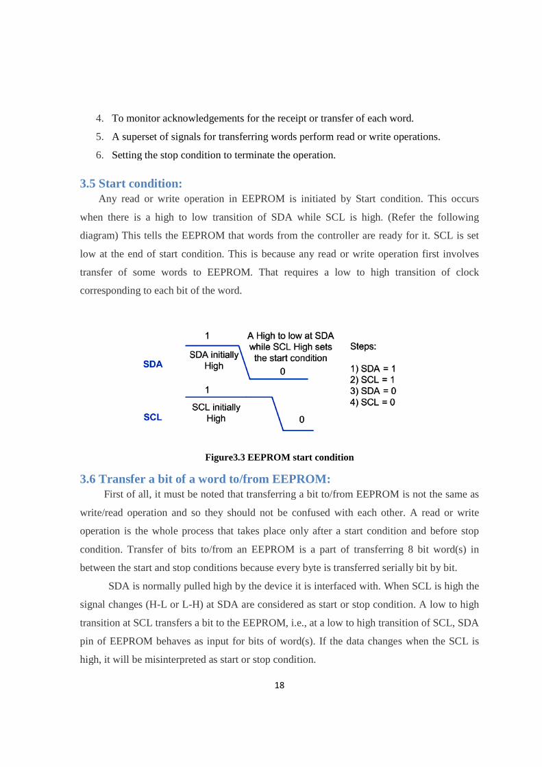
3.5 Start condition: Any read or write operation in EEPROM is initiated by Start condition. This occurs
when there is a high to low transition of SDA while SCL is high. (Refer the following
diagram) This tells the EEPROM that words from the controller are ready for it.
low at the end of start condition. This is because any read or write operation first involves
transfer of some words to EEPROM. That requires a low to high transition of clock
corresponding to each bit of the word.
3.6 Transfer a bit of a word to/from EEPROM: First of all, it must be noted that transferring a bit to/from EEPROM is not the same as
write/read operation and so they should not be confused
operation is the whole process that takes place only after a start condition and before stop
condition. Transfer of bits to/from an EEPROM is a part of transferring 8 bit word(s) in
between the start and stop conditions bec
SDA is normally pulled high by the device it is interfaced with. When SCL is high the
signal changes (H-L or L-
transition at SCL transfers a bit to the EEPROM
pin of EEPROM behaves as
high, it will be misinterpreted as start or stop condition.
18
To monitor acknowledgements for the receipt or transfer of each word.
A superset of signals for transferring words perform read or write operations.
Setting the stop condition to terminate the operation.
Any read or write operation in EEPROM is initiated by Start condition. This occurs
when there is a high to low transition of SDA while SCL is high. (Refer the following
diagram) This tells the EEPROM that words from the controller are ready for it.
low at the end of start condition. This is because any read or write operation first involves
transfer of some words to EEPROM. That requires a low to high transition of clock
corresponding to each bit of the word.
Figure3.3 EEPROM start condition
Transfer a bit of a word to/from EEPROM: First of all, it must be noted that transferring a bit to/from EEPROM is not the same as
write/read operation and so they should not be confused with each other. A read or write
operation is the whole process that takes place only after a start condition and before stop
condition. Transfer of bits to/from an EEPROM is a part of transferring 8 bit word(s) in
between the start and stop conditions because every byte is transferred serially bit by bit.
SDA is normally pulled high by the device it is interfaced with. When SCL is high the
-H) at SDA are considered as start or stop condition.
L transfers a bit to the EEPROM, i.e., at a low to high transition of SCL,
of EEPROM behaves as input for bits of word(s). If the data changes when the SCL is
high, it will be misinterpreted as start or stop condition.
To monitor acknowledgements for the receipt or transfer of each word.
A superset of signals for transferring words perform read or write operations.
Any read or write operation in EEPROM is initiated by Start condition. This occurs
when there is a high to low transition of SDA while SCL is high. (Refer the following
diagram) This tells the EEPROM that words from the controller are ready for it. SCL is set
low at the end of start condition. This is because any read or write operation first involves
transfer of some words to EEPROM. That requires a low to high transition of clock
First of all, it must be noted that transferring a bit to/from EEPROM is not the same as
with each other. A read or write
operation is the whole process that takes place only after a start condition and before stop
condition. Transfer of bits to/from an EEPROM is a part of transferring 8 bit word(s) in
ause every byte is transferred serially bit by bit.
SDA is normally pulled high by the device it is interfaced with. When SCL is high the
H) at SDA are considered as start or stop condition. A low to high
, i.e., at a low to high transition of SCL, SDA
for bits of word(s). If the data changes when the SCL is
Page 27
Figure
At high to low transition of SCL a bit is transferred from the EEPROM
behaves as output for bits of word(s) or acknowledg
SCL. When SCL is low again the data change is valid, i.e., when bits of a word are to be read
or write, they are differentiated by the low of the SCL.
3.7 Transfer of a word to/from EEPROM: By sending or receiving eight bits, a complete word is sent to or received by the
EEPROM. When sending a word, the acknowledgement from the EEPROM must be
checked. There should a clock (high to low transition from an initial low) between two
words.
Figure
19
Figure3.4 Transfer a bit of a word to/from EEPROM
At high to low transition of SCL a bit is transferred from the EEPROM
for bits of word(s) or acknowledgement at high to low transition
SCL. When SCL is low again the data change is valid, i.e., when bits of a word are to be read
or write, they are differentiated by the low of the SCL.
Transfer of a word to/from EEPROM: By sending or receiving eight bits, a complete word is sent to or received by the
EEPROM. When sending a word, the acknowledgement from the EEPROM must be
checked. There should a clock (high to low transition from an initial low) between two
igure3.5 Transfer of a word to/from EEPROM
Transfer a bit of a word to/from EEPROM
At high to low transition of SCL a bit is transferred from the EEPROM i.e. the SDA pin
ement at high to low transition of the
SCL. When SCL is low again the data change is valid, i.e., when bits of a word are to be read
By sending or receiving eight bits, a complete word is sent to or received by the
EEPROM. When sending a word, the acknowledgement from the EEPROM must be
checked. There should a clock (high to low transition from an initial low) between two
Page 28
3.8 Monitoring Acknowledgement bit: When a word is sent to the EEPROM, it sends back a zero (0) to tell the controller that
the word has been received successfully by it. The
by sending a high to low transition at SCL. Acknowledgement bit must be checked every
time a word is sent to the EEPROM.
3.9 Read/write operation: A sequential transfer of words from/to the EEPROM constitu
read or write operation supported by the EEPROM can be accomplished by sending and/or
receiving a sequence of words to/from the EEPROM. There is a fixed set of words which
need to be sent to and/or received by the EEPROM corres
operation.
Figure
3.10 Stop condition: A stop condition is provided to terminate a read or write operation. A low to high
SDA when SCL is high
20
Monitoring Acknowledgement bit: When a word is sent to the EEPROM, it sends back a zero (0) to tell the controller that
the word has been received successfully by it. The controller reads this acknowledgement bit
by sending a high to low transition at SCL. Acknowledgement bit must be checked every
time a word is sent to the EEPROM.
Read/write operation: A sequential transfer of words from/to the EEPROM constitutes the read/write. Thus any
read or write operation supported by the EEPROM can be accomplished by sending and/or
receiving a sequence of words to/from the EEPROM. There is a fixed set of words which
need to be sent to and/or received by the EEPROM corresponding to each read and write
Figure3.6 Read/write operation of EEPROM
A stop condition is provided to terminate a read or write operation. A low to high
SDA when SCL is high sets the stop condition.
Figure3.7 Stop condition of EEPROM
When a word is sent to the EEPROM, it sends back a zero (0) to tell the controller that
controller reads this acknowledgement bit
by sending a high to low transition at SCL. Acknowledgement bit must be checked every
tes the read/write. Thus any
read or write operation supported by the EEPROM can be accomplished by sending and/or
receiving a sequence of words to/from the EEPROM. There is a fixed set of words which
ponding to each read and write
A stop condition is provided to terminate a read or write operation. A low to high transition of
Page 29
3.11 Memory addressing: In 24C16, the 8 bit words are arranged in 32 pages of 8 bytes each. The word/page
address should be sent to the EEPROM to identify the location of memory to be read or
written. The word location is specified by three bits since the total number of
words/bytes is 8 (23). Similarly, the page location is given by five bits since the total number
of available pages is 32 (2
word location in a page, while the higher five bytes (D
Figure
3.12 Clocking: When a sequence of words is transferred to EEPROM, a clock is needed to be sent by
the controller after transmission of each word. This is required so that the controller can
receive its acknowledgement. Clock is just a high transition followed by a
SCL when the initial clock signal is low
3.13 Byte write operation: The Byte Write operation programs a single byte of the EEPROM memory. It
involves following sequences of instructions to be sent to the EEPROM by the
microcontroller:
21
Memory addressing: In 24C16, the 8 bit words are arranged in 32 pages of 8 bytes each. The word/page
address should be sent to the EEPROM to identify the location of memory to be read or
written. The word location is specified by three bits since the total number of
). Similarly, the page location is given by five bits since the total number
of available pages is 32 (25). The lower three bits (D0-D2) of the word address identify the
word location in a page, while the higher five bytes (D3-D7) identify the page location.
Figure3.8 Memory addressing of EEPROM
When a sequence of words is transferred to EEPROM, a clock is needed to be sent by
the controller after transmission of each word. This is required so that the controller can
receive its acknowledgement. Clock is just a high transition followed by a
SCL when the initial clock signal is low.
Figure3.9 Clocking condition
Byte write operation: The Byte Write operation programs a single byte of the EEPROM memory. It
sequences of instructions to be sent to the EEPROM by the
In 24C16, the 8 bit words are arranged in 32 pages of 8 bytes each. The word/page
address should be sent to the EEPROM to identify the location of memory to be read or
written. The word location is specified by three bits since the total number of available
). Similarly, the page location is given by five bits since the total number
D2) of the word address identify the
D7) identify the page location.
When a sequence of words is transferred to EEPROM, a clock is needed to be sent by
the controller after transmission of each word. This is required so that the controller can
receive its acknowledgement. Clock is just a high transition followed by a low transition of
The Byte Write operation programs a single byte of the EEPROM memory. It
sequences of instructions to be sent to the EEPROM by the
Page 30
22
1. Set start condition
2. Send device address byte (specify write operation)
3. Clock
4. Send word address
5. Clock
6. Send data byte
7. Clock
8. Send stop condition
9. clock
3.14 Random read operation: The random read operation reads the data from a word address clocked in by the
following sequence of instructions to be sent to/from the EEPROM by/to the controller.
1. Set start condition
2. Send device address byte (specify write operation)
3. Clock
4. Send word address
5. Clock
6. Set start condition
7. Send device address byte (specify read operation)
8. Clock
9. Read data byte
10. Clock
11. Stop condition
Page 31
23
3.15 KEIL Micro vision Logic Analyzer output:
Figure3.10 START & Single write byte
Figure3.11 STOP & Single read byte
Page 32
24
Figure3.12 After read (FF)
3.16 Summary: The interfacing between microcontroller (AT89C51) and EEPROM (AT24C16) through I2C
bus gives a brief idea of I2C protocol system. The microcontroller acts as master and
EEPROM acts as a slave device of I2C components. The program written in C language is
simulated in KEIL Micro vision 3 software tool by linking with the microcontroller board
and the output for data sent (READ) and receive (WRITE) has verified.
Page 33
25
CHAPTER-4
I 2C BUS CONTROLLER DESIGN
Page 34
26
4.1 Introduction: This thesis is aimed at designing of a Master controller for I2C bus using the Verilog
Hardware Description Language (HDL). I2C is a two-wire, bi-directional serial bus that
provides a simple and efficient method of data exchange between devices. It is most suitable
for applications requiring occasional communication over a short distance between many
devices. The I2C standard is a true multi-master bus including collision detection and
arbitration that prevents data corruption if two or more masters attempt to control the bus
simultaneously. This core, however, supports only single master operations, in which the
core is the master. The I2C interface uses a serial data line (SDA) and a serial clock line
(SCL) for data transfers.
The use of Verilog HDL has many advantage compared to the traditional schematic based
design
• Designs can be described at very abstract level using HDL. Designer can write his
design description without choosing any specific fabrication technology. If a new
technology emerges, designers do not need to redesign the circuit. He simply input
the design program to the logic synthesis tool and create a new gate level netlist using
the new fabrication technology. The logic synthesis tool will optimize the circuit in
area and timing for the new technology.
• By describing the design in HDL, functional verification of the design can be done
early in the design cycle. Since designers work at the high level language, they can
optimize and modify the design module until it meets the desired functionality. Most
of the design bugs are eliminated at this point.
4.2 I2C Protocol: Normally, a standard communication protocol consists of four parts:
1) START signal generation
2) Slave address transfer
3) Data transfer
4) STOP signal generation
Page 35
27
4.3 Design steps: � The functional description of I2C master has to be described in the Verilog HDL. That
is called design module / core.
� The test bench program has to be developed to test the design module. The test bench
gives the input to the design module & verifies the outputs. The test bench has to be
written in such way to check the design module in all possible conditions.
� Verilog simulator tool is used to verify the design functioning. (Simulation).
4.4 Design Goals and Limitation: The following goals were considered during this design:
• I2C bus speeds of 100kbits/sec and 400kbits/sec
• I2C 7-bit addressing
• Multiple I2C masters on one I2C bus
• Up to 256-byte I2C transactions
• Compatible with any number of slaves
• Operates wide range of input frequencies
• Programmable configuration registers
• Hierarchical HDL design for simple user modification
• Fully automated, self-checking HDL test bench for ease of verification.
The I2C Bus Master Controller does not support the following features:
• High speed mode 3.4 Mbps
• Mixed speed modes on one bus
• 10-bit addressing
• Master Controller cannot be used as an I2C slave device
Page 36
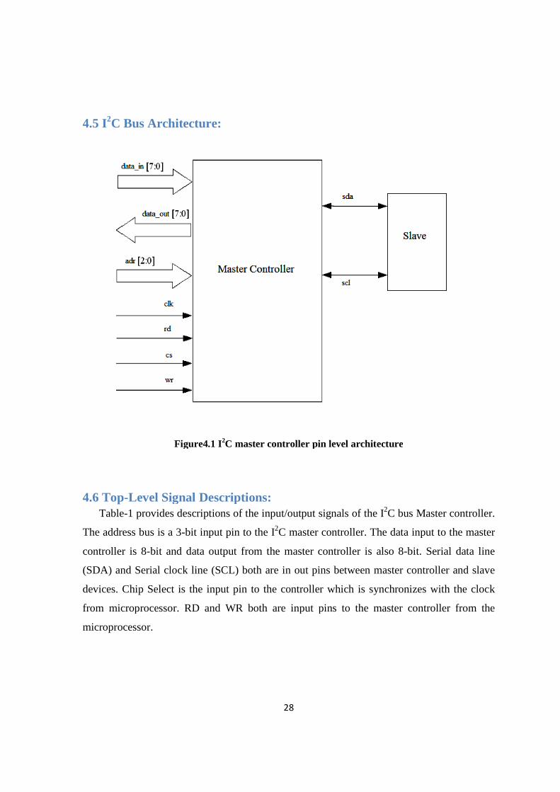
4.5 I2C Bus Architecture:
Figure
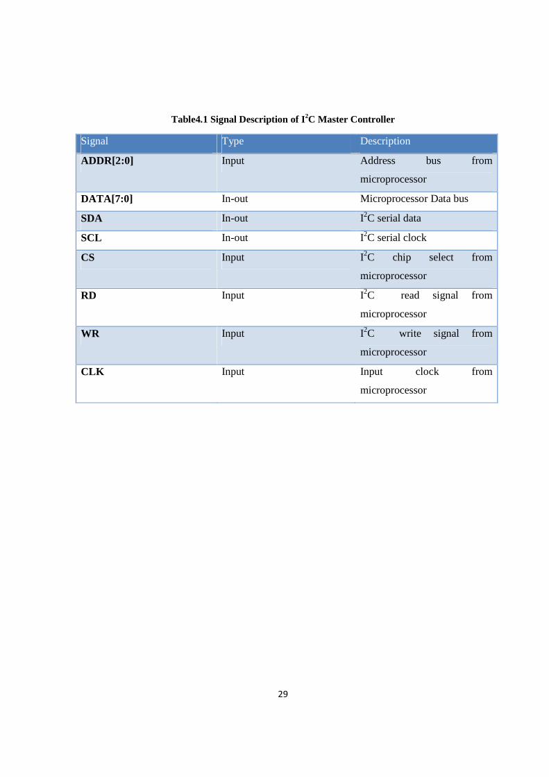
4.6 Top-Level Signal Descriptions: Table-1 provides descriptions of the input/output signals of the I
The address bus is a 3-bit inpu
controller is 8-bit and data output from the master controller is also 8
(SDA) and Serial clock line (SCL) both are in out pins between master controller and slave
devices. Chip Select is the
from microprocessor. RD and WR both are input pins to
microprocessor.
28
C Bus Architecture:
Figure4.1 I2C master controller pin level architecture
Level Signal Descriptions: provides descriptions of the input/output signals of the I2C bus Master controller.
bit input pin to the I2C master controller. The data input to the master
bit and data output from the master controller is also 8
(SDA) and Serial clock line (SCL) both are in out pins between master controller and slave
Chip Select is the input pin to the controller which is synchronizes
from microprocessor. RD and WR both are input pins to the master controller from the
C master controller pin level architecture
C bus Master controller.
The data input to the master
bit and data output from the master controller is also 8-bit. Serial data line
(SDA) and Serial clock line (SCL) both are in out pins between master controller and slave
synchronizes with the clock
the master controller from the
Page 37
29
Table4.1 Signal Description of I2C Master Controller
Signal Type Description
ADDR[2:0] Input Address bus from
microprocessor
DATA[7:0] In-out Microprocessor Data bus
SDA In-out I2C serial data
SCL In-out I2C serial clock
CS Input I2C chip select from
microprocessor
RD Input I2C read signal from
microprocessor
WR Input I2C write signal from
microprocessor
CLK Input Input clock from
microprocessor
Page 38
30
4.7 Register Definitions: This I2C Master Controller core uses the following registers:
Table4.2 Register Description of I2C Master Controller
Register No. of Bit Description
out_sda 1 Sda output
Out_scl 1 Scl output
In_buffer 8[7:0] Input buffer
Buffer 8[7:0] Buffer out_data
Ack 1 Acknowledgement bit
Speed 1 Speed of bus
(400kbps/100kbps)
I 2C_clk 1 I2C master controller clock
Clk_count 7[6:0] Clock counts by master
state 3[2:0] State of data
Next state 3[2:0] Next state of data
State_count 6[5:0] Number of states for
transaction
Bit_count 3[2:0] Number of data bits for
transaction
Page 39
31
4.8 Flowchart:
Figure4.2 Communication application flowchart
4.8 Simulation Results: The verilog code for I2C master controller is compiled in the Mentor Graphics Questa 64 6.5b software tool. The test bench of this module is simulated and followings are the results.
Here in all the cases I have taken clock frequency of 20MHZ that is time period of 50ns and duty cycle of 50%.
Figure4.3 START condition
Page 40
32
Figure4.4 Master transmits to slave receiver (WRITE).
Figure4.5 Master transmits to slave receiver (WRITE).
Page 41
33
Figure4.6 Acknowledgement condition
Figure4.7 Master transmits to slave receiver (WRITE).
Page 42
34
Figure4.8 Master transmits to slave receiver (WRITE).
Figure4.9 Repeated start condition
Page 43
35
Figure4.10 Master reads slave (READ)
Figure4.11 Master reads slave (READ)
Page 44
36
Figure4.12 Master reads slave (READ)
Figure4.13 Master reads slave (READ)
Page 45
37
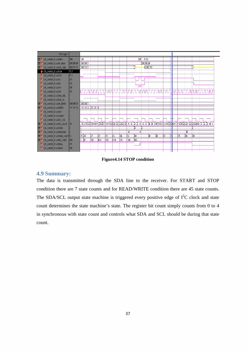
Figure4.14 STOP condition
4.9 Summary: The data is transmitted through the SDA line to the receiver. For START and STOP
condition there are 7 state counts and for READ/WRITE condition there are 45 state counts.
The SDA/SCL output state machine is triggered every positive edge of I2C clock and state
count determines the state machine’s state. The register bit count simply counts from 0 to 4
in synchronous with state count and controls what SDA and SCL should be during that state
count.
Page 46
38
CHAPTER- 5
CONCLUSION AND SUGGESTS FUTURE WORK
Page 47
39
5.1 Conclusion: The results of simulation and desired behavior of the I2C bus controller agree. The
interfacing of microcontroller (master) and serial EEPROM (slave) has done by using I2C
bus which elaborates that I2C components are working as our desired conditions. The design
of I2C controller using verilog HDL, simplifies the design process. The designer can write his
design description without choosing any specific fabrication technology. If a new technology
emerges, designers do not need to redesign the circuit. He simply input the design program to
the logic synthesis tool and creates a new gate level netlist using the new fabrication
technology. The logic synthesis tool will optimize the circuit in area and timing for the new
technology.
5.2 Future work: � Dumping of Verilog code to FPGA to realize the exact hardware of the circuit.
� Verification of I2C bus using system verilog based open verification methodology.
� Interfacing of different I2C components like ADC/DAC, RTC & EEPROM with
Microcontroller through I2C bus at a time and the result to be displayed on LCD.
Page 48
40
References: [1] The I2C -Bus specifications version 2.1 January 2000
http://www.semiconductors.philips.com/buses/i2c
[2] UM10204 I2C -bus specification and user manual Rev. 03 — 19 June 2007
[3] I2C bus Inter Integrated Circuits bus by Philips Semiconductors
[4] Embedded Platform Excalibur Altera, http://www.altera.com
[5]PCF 8584, I2C bus controller datasheet,
http://www.semiconductor.philips.com
[6] The 8051 Microcontroller and Embedded Systems, using Assembly and C
by Muhammed Ali Mazidi, Janice Gillispie Mazidi & Rolin D. Mckinlay,
second Edition, Pearson Education.
[7] A Verilog HDL Primer, by J. Bhaskar, second Edition, BSP.
[8] www.latticesemi.com, I2C Master Controller reference design,
[9] www.mentor.com, Concise Manual for the Questasim simulator.
[10] D. Paret: Le bus I2C, de la théorie à la pratique, ISBN2100017179, ed.
DUNOD, Paris 1993
[11] SAA1064, 4-digit Led-driver with I2C bus interface datasheet,
http://www.semicondutors.philips.com
[12] M. D. Ciletti. Advanced Digital Design with the Verilog HDL, Publishing
House of Electronics Industry, 2004.4
[13] IEEE Computer Society. IEEE Standard Verilog® Hardware Description
Language, IEEE Std 1364-2001, The Institute of Electrical and Electronics
Engineers, Inc,28 September 2001
[14] R. Herveille. I2C-Master Core Specification, Rev. 0.9,
2003.7
Page 49
41
[15]http://www.engineersgarage.com/microcontroller/8051projects/interface-
serial-eeprom-24c02-AT89C51-circuit.
[16]http://www.charmedlabs.com/index.php?option=com_smf&Itemid=36&top
ic=640.0.