93
March 2018
Design and Optimisation of Gap Waveguide
Components through Space Mapping
by
Cliord Sibanda
Thesis presented in partial fullment of the requirements forthe degree of Master of Engineering (Electronic) in the
Faculty of Engineering at Stellenbosch University
Supervisor: Prof. D. I. L. De Villiers
March 2018
Declaration
By submitting this thesis electronically, I declare that the entirety of the workcontained therein is my own, original work, that I am the sole author thereof(save to the extent explicitly otherwise stated), that reproduction and pub-lication thereof by Stellenbosch University will not infringe any third partyrights and that I have not previously in its entirety or in part submitted it forobtaining any qualication.
March 2018Date: . . . . . . . . . . . . . . . . . . . . . . . . . . . . . . .
Copyright© 2018 Stellenbosch UniversityAll rights reserved.
i
Stellenbosch University https://scholar.sun.ac.za

Abstract
Design and Optimisation of Gap Waveguide Componentsthrough Space Mapping
C. Sibanda
Department of Electrical and Electronic Engineering,
University of Stellenbosch,
Private Bag X1, Matieland 7602, South Africa.
Thesis: MEng (Elec)
January 2018
This thesis presents a detailed approach and method to design and optimiseridge and groove gap waveguide components using input space mapping. Gapwaveguides are expected to contribute signicantly towards the implementa-tion of microwave components especially for the millimetre and sub-millimetrewavelengths. This is due to their manufacturing exibility, low loss andgood power handling capabilities when compared to conventional rectangularwaveguides and transmission lines.
The application of the space mapping technique to speed up the design andoptimisation of gap waveguide components, which traditionally rely heavilyon slower full wave simulations of the structures, is demonstrated through theuse of simple circuit models. The application of a stripline model to designand optimise ridge gap waveguide components through space mapping ispresented. Input space mapping, which is the most basic and original versionof space mapping, is successfully applied in the optimisation of a 3-dB ridgegap waveguide power divider and hybrid coupler using a computationallycheap but faster stripline model.
A transmission line model is also used in the design and optimisation ofthird and fth order narrow band ridge and groove gap waveguide coupledresonator Chebychev bandpass lters using an in-house input space mappingcode. The bandpass lters are successfully designed and optimised in arelatively short time through the use of input space mapping with convergentresults after only a few computational electromagnetic (CEM) simulations.
ii
Stellenbosch University https://scholar.sun.ac.za

ABSTRACT iii
The results show that using the calculated design parameter values in lters,and generally in gap waveguide component designs, in most cases doesnot give an optimum design. The design parameters need to be tuned oroptimised to meet the design specications. The transmission line model isshown to give accurate results for the narrow band Chebychev bandpass lters.
The lter examples are directly optimised using a built-in computer sim-ulation technology (CST) optimiser and the results are compared with thoseof input space mapping. The input space mapping technique is shown to giveconvergent results which meet the design specications and is signicantlyfaster than the conventional full-wave optimisation approach.
Stellenbosch University https://scholar.sun.ac.za

Opsomming
Ontwerp en Optimering van Gaping-GoleierKomponente deur Ruimtekartering
(Design and Optimisation of Gap Waveguide Components through Space Mapping)
C. Sibanda
Departement Elektriese en Elektroniese Ingenieurswese,
Universiteit van Stellenbosch,
Privaatsak X1, Matieland 7602, Suid Afrika.
Tesis: MIng (Elec)
Januarie 2018
Hierdie tesis bied 'n gedetailleerde benadering en metode aan vir die ontwerpen optimering van rif en gleuf gaping-goleier komponente deur intree ruim-tekartering. Daar word verwag dat gaping-goleiers 'n beduidende bydra salmaak in die implementering van mikrogolf komponente - veral in die millime-ter en sub-millimeter golengte bande. Dit is te danke aan die vervaardigingstegniek buigbaarheid, lae verliese en goeie drywing hanterings vermoë invergelyking met konvensionele reghoekige goleiers en transmissielyne.
Die toepassing van die ruimtekarteringstegniek op die versnelde ontwerpen optimering van gaping-goleier komponente, wat tradisioneel swaar steunop volgolf numeriese elektromagnetiese simulasies in hulle ontwerp, word deurdie gebruik van eenvoudige stroombaan modelle geïllustreer. Die toepassingvan 'n strooklyn model om rif gaping goleier komponente te ontwerp enoptimeer word voorgehou. Intree ruimte kartering, wat die eenvoudigste enoorspronklike weergawe van ruimtekartering is, word suksesvol toegepas indie optimering van 'n 3-dB rif gaping-goleier drywingsverdeler en hibriedekoppelaar deur van 'n numeries goedkoop en vinniger strooklyn model gebruikte maak.
'n Transmissielyn model word ook gebruik in die ontwerp en optimeringvan derde en vyfde orde nouband rif en gleuf gaping-goleier gekoppelderesoneerder Chebyshev banddeurlaatlters deur van 'n in-huis ruimtekarteringkode gebruik te maak. Die banddeurlaatlters word in 'n relatiewe kort
iv
Stellenbosch University https://scholar.sun.ac.za

OPSOMMING v
tydperk ontwerp en geoptimeer deur van intree ruimtekartering gebruikte maak, en gekonvergeerde resultate word na slegs 'n paar numerieseelektromagnetiese simulasie lopies verkry. Die resultate toon dat om dieoorspronklike ontwerpsparameters te gebruik in lters, en in die algemeen ingaping-goleier komponente, in meeste gevalle nie die optimum resultate totgevolg het nie. Die ontwerpsparameters moet ingestem en geoptimeer wordom die ontwerpspesikasies te haal. Daar word getoon dat die transmissielynmodelle redelike akkurate resultate vir die nouband Chebychev lters lewer.
Die lter voorbeelde word ook direk geoptimeer deur van die ingeboude op-timeerder in CST gebruik te maak, en die resultate word vergelyk met die vandie intree ruimtekartering. Daar word sodoende getoon dat die intree ruim-tekarterings tegniek konvergente resultate lewer, wat die ontwerp spesikasiehaal, en dat dit beduidend vinniger is as die konvensionele volgolf optimeringstegniek.
Stellenbosch University https://scholar.sun.ac.za

Contents
Declaration i
Abstract ii
Opsomming iv
Contents vi
List of Figures viii
List of Tables xi
Nomenclature xii
1 Introduction 1
1.1 Introduction . . . . . . . . . . . . . . . . . . . . . . . . . . . . . 1
2 Gap Waveguide Technology 5
2.1 Introduction . . . . . . . . . . . . . . . . . . . . . . . . . . . . . 5
3 Space Mapping 11
3.1 Introduction . . . . . . . . . . . . . . . . . . . . . . . . . . . . . 113.2 Input Space Mapping . . . . . . . . . . . . . . . . . . . . . . . . 143.3 Design of Microstrip Bandstop Stub Filter Using Space Mapping 15
4 Optimisation of Gap Waveguide Components through Space
Mapping 20
4.1 Introduction . . . . . . . . . . . . . . . . . . . . . . . . . . . . . 204.2 T-Junction Power Divider . . . . . . . . . . . . . . . . . . . . . 284.3 Optimisation of 3-dB Ridge Gap Waveguide T-Junction Power
Divider Using Input Space Mapping . . . . . . . . . . . . . . . . 294.4 Design and Optimisation of a 3-dB Ridge Gap Waveguide Hy-
brid Coupler Using Input Space Mapping . . . . . . . . . . . . 34
5 Optimisation of Microwave Gap Waveguide Bandpass Fil-
ters Using Space Mapping 41
vi
Stellenbosch University https://scholar.sun.ac.za

CONTENTS vii
5.1 Bandpass Filter Basics . . . . . . . . . . . . . . . . . . . . . . . 415.2 Narrow Band Microwave Groove Gap Waveguide Coupled Res-
onator Bandpass Filters . . . . . . . . . . . . . . . . . . . . . . 485.3 Third Order Narrow Band Microwave Ridge Gap Waveguide
Coupled Resonators Bandpass Filter . . . . . . . . . . . . . . . 66
6 Conclusion 75
List of References 78
Stellenbosch University https://scholar.sun.ac.za

List of Figures
2.1 Ridge gap waveguide dimensions and propagation regions . . . . . . 62.2 Groove gap waveguide propagation regions . . . . . . . . . . . . . . 62.3 Unit cell . . . . . . . . . . . . . . . . . . . . . . . . . . . . . . . . . 72.4 Dispersion graph for a double transition unit cell . . . . . . . . . . 82.5 Double transition ridge gap waveguide . . . . . . . . . . . . . . . . 82.6 S-parameter results for double transition ridge gap waveguide . . . 92.7 E-eld total amplitudes for double transition for 9 - 16 GHz . . . . 102.8 E-eld amplitudes for double transition for 17 - 22 GHz . . . . . . . 10
3.1 MWO stopband lter coarse model 3-D diagram . . . . . . . . . . 163.2 MWO |S21| coarse model response curve . . . . . . . . . . . . . . . 163.3 CST 3-D diagram of the microstrip lter . . . . . . . . . . . . . . . 173.4 CST |S21| ne model response curve . . . . . . . . . . . . . . . . . 173.5 Coarse, ne and aligned surrogate models . . . . . . . . . . . . . . 183.6 CST |S21| ne model response curve . . . . . . . . . . . . . . . . . 19
4.1 Ideal stripline and TEM propagation mode . . . . . . . . . . . . . . 214.2 Half stripline . . . . . . . . . . . . . . . . . . . . . . . . . . . . . . 214.3 Gap waveguides and their equivalent rectangular waveguides . . . 244.4 Ridge gap/ridged rectangular waveguides dispersion graphs for h
= 0.5 . . . . . . . . . . . . . . . . . . . . . . . . . . . . . . . . . . 254.5 Ridge gap/ridged rectangular waveguides dispersion graphs for h
= 1 . . . . . . . . . . . . . . . . . . . . . . . . . . . . . . . . . . . 254.6 Ridge gap/ridged rectangular waveguides dispersion graphs for h
= 2 . . . . . . . . . . . . . . . . . . . . . . . . . . . . . . . . . . . 264.7 Ridge gap/ridged rectangular waveguides dispersion graphs for h
= 3 . . . . . . . . . . . . . . . . . . . . . . . . . . . . . . . . . . . 264.8 Groove/hollow waveguide dispersion graphs . . . . . . . . . . . . . 274.9 (a) Groove waveguide port arrangement and (b )ridge waveguide
port arrangement . . . . . . . . . . . . . . . . . . . . . . . . . . . 274.10 Best waveguide port conguration and dimensions . . . . . . . . . 284.11 Transmission line model of a power divider . . . . . . . . . . . . . . 294.12 MWO stripline coarse model schematic . . . . . . . . . . . . . . . 314.13 MWO stripline coarse model response . . . . . . . . . . . . . . . . 31
viii
Stellenbosch University https://scholar.sun.ac.za
LIST OF FIGURES ix
4.14 CST 3-D ne model diagram . . . . . . . . . . . . . . . . . . . . . 324.15 Cross sectional dimensions of double and single ridged waveguides . 334.16 CST ne model rst iteration . . . . . . . . . . . . . . . . . . . . . 344.17 CST ne model second iteration . . . . . . . . . . . . . . . . . . . 354.18 Hybrid coupler schematic diagram . . . . . . . . . . . . . . . . . . 364.19 MWO coupler coarse model schematic diagram . . . . . . . . . . . 374.20 MWO coupler coarse model S-parameters . . . . . . . . . . . . . . 384.21 CST coupler 3-D ne model . . . . . . . . . . . . . . . . . . . . . . 384.22 CST coupler ne model initial S-parameters . . . . . . . . . . . . . 394.23 Alignment step and the aligned models . . . . . . . . . . . . . . . 394.24 Second iteration and the ne model S-parameters response . . . . . 40
5.1 Chebyshev transmission function response . . . . . . . . . . . . . . 425.2 Lumped element lowpass lter circuit . . . . . . . . . . . . . . . . 445.3 Impedance Inverter model for Chebyshev bandpass lter . . . . . . 455.4 K-Inverter equivalent lumped elements circuit . . . . . . . . . . . . 455.5 Electric wall and magnetic wall symmetry method . . . . . . . . . 465.6 Two resonator arrangement for the S-parameter method . . . . . . 495.7 Main-line coupling S-parameters . . . . . . . . . . . . . . . . . . . 495.8 Approximated graph of K and inter-resonator distance s (mm) . . 505.9 Eiegemmode solver method . . . . . . . . . . . . . . . . . . . . . . 515.10 Mode 1 . . . . . . . . . . . . . . . . . . . . . . . . . . . . . . . . . 525.11 Mode 2 . . . . . . . . . . . . . . . . . . . . . . . . . . . . . . . . . 525.12 Eigenmode solver method for K and s . . . . . . . . . . . . . . . . 535.13 Group delay method with resonator and SMA port distance x . . . 545.14 Typical circuit model of source and rst resonator . . . . . . . . . 545.15 Group delay of the S11 Phase . . . . . . . . . . . . . . . . . . . . . 565.16 Group delay values and distance x . . . . . . . . . . . . . . . . . . 575.17 Group delay frequency and distance x . . . . . . . . . . . . . . . . 575.18 External quality factor Qex and SMA port position x . . . . . . . . 585.19 Third order bandpass lter coarse model . . . . . . . . . . . . . . . 595.20 Third order bandpass lter coarse model S-parameters . . . . . . . 595.21 Fine model and design parameters . . . . . . . . . . . . . . . . . . 605.22 Third order rst iteration . . . . . . . . . . . . . . . . . . . . . . . 615.23 Third order last iteration . . . . . . . . . . . . . . . . . . . . . . . 615.24 Space mapping and Direct optimisation Fine model S-parameters . 625.25 Fifth order coarse model schematic . . . . . . . . . . . . . . . . . . 635.26 Fifth order coarse model S-parameters . . . . . . . . . . . . . . . . 635.27 Fifth order ne model . . . . . . . . . . . . . . . . . . . . . . . . . 645.28 First iteration evaluation response of the ne model . . . . . . . . . 645.29 Last iteration response of the ne model . . . . . . . . . . . . . . . 655.30 Space mapping and Direct optimisation ne model S-parameters . . 655.31 Ridge gap waveguide view and dimensions . . . . . . . . . . . . . . 675.32 Ridge gap waveguide resonators for main-line coupling . . . . . . . 68
Stellenbosch University https://scholar.sun.ac.za

LIST OF FIGURES x
5.33 Eigenmode solver method for K and s . . . . . . . . . . . . . . . . 685.34 Group delay method for Qex and distance x . . . . . . . . . . . . . 695.35 External quality factor Qex and distance x . . . . . . . . . . . . . . 705.36 Coarse model schematic diagram . . . . . . . . . . . . . . . . . . . 715.37 Coarse model S-parameters . . . . . . . . . . . . . . . . . . . . . . 715.38 Fine model and design parameters . . . . . . . . . . . . . . . . . . 725.39 S-parameters for the rst iteration . . . . . . . . . . . . . . . . . . 735.40 S-parameters for the last iteration . . . . . . . . . . . . . . . . . . 735.41 Space mapping and Direct optimisation ne model S-parameters . 74
Stellenbosch University https://scholar.sun.ac.za

List of Tables
3.1 Alignment between coarse and ne models using Rs = Rc + c . . . . 183.2 New stub length design value . . . . . . . . . . . . . . . . . . . . . 18
4.1 Alignment step . . . . . . . . . . . . . . . . . . . . . . . . . . . . . 374.2 New coarse model design values . . . . . . . . . . . . . . . . . . . . 39
5.1 Coupling K and corresponding inter-resonator distance s . . . . . . 505.2 Filter initial and optimum design parameter values . . . . . . . . . 625.3 Filter initial and nal design parameter values . . . . . . . . . . . . 665.4 Filter initial and optimum design parameter values . . . . . . . . . 72
xi
Stellenbosch University https://scholar.sun.ac.za

Nomenclature
Abbreviations
CEM Computational Electromagnetic
CST Computer Simulation Technology
E Electric
EM Electromagnetic
MWO Microwave Oce
PEC Perfect Electric Conductor
PMC Perfect Magnetic Conductor
TE Transverse Electric
TEM Transverse Electromagnetic
xii
Stellenbosch University https://scholar.sun.ac.za

Chapter 1
Introduction
1.1 Introduction
The main objective of this thesis, is the application of space mapping in thedesign and optimisation of microwave gap waveguide components. Most micro-wave components and circuits are mainly based on conventional waveguidesand transmission lines. However, for the millimetre and sub-millimetre wave-lengths, the above-mentioned technologies have high losses, are dicult tofabricate and their production cost can be high. For example, microstrip trans-mission line based microwave components and devices for the millimetre andsub-millimetre wavelengths have high losses due to the presence of dielectricin microstrip.
1.1.1 Hollow Rectangular Waveguides
At millimetre and sub-millimetre waves range, the fabrication of hollow rect-angular waveguides can be very dicult. Often joint imperfections may re-sult from joining of plates in the fabrication process. These mechanical jointimperfections can result in eld leaks, poor electrical contact and can alsocompromise the waterproong, leading to oxidation of the waveguide compo-nent which may degrade its performance. Poor electrical contact between theplates in rectangular waveguide is one of the common sources of passive inter-modulation [1]. Hence high precision machining techniques and good align-ment of metal plates are required for fabrication and mechanical assemble ofconventional hollow waveguides for millimetre and sub-millimetre wavelengthmicrowave applications. This often leads to high production cost and de-lays if large volumes are to be produced. Therefore, the use of conventionalwaveguides may not be a good economic option for the millimetre and sub-millimetre microwave frequency range.
1
Stellenbosch University https://scholar.sun.ac.za

CHAPTER 1. INTRODUCTION 2
1.1.2 Gap Waveguide Technology
This thesis will look at application of space mapping for the design andoptimisation of new gap waveguide microwave components. Gap waveguideis a new technology that is mainly used to make low-loss components andcircuits at millimetre and sub-millimetre waves. There are three mainmajor gap waveguides types. These are the ridge, groove and microstripwaveguides [2]. This thesis will only cover the ridge and groove gap waveguides.
The gap waveguides are expected to contribute signicantly towards themicrowave system components especially for the millimetre and sub-millimetrewavelengths. This is due to their manufacturing exibility, low loss and goodpower handling capabilities. There are gap waveguide components thathave already been designed, measured and veried. These include the ridgegap waveguide power divider [3, 4] and the groove gap waveguide coupledresonator lters with high Q resonators [5]. Other designed componentsinclude a V-band groove gap waveguide diplexer [6], wide band slot antennaarray with single layer corporate feed network with ridge gap waveguidetechnology [7] and a 76 GHz multi-layered phased array antenna using anon-metal contact metamaterial waveguide [8]. The gap waveguide technologycan also be used for packaging of the microstrip line circuits for suppressingthe unwanted radiations with no cavity resonance over a wide bandwidth[9]. Active components like ampliers and microwave monolithic integratedcircuits (MMICs) can be included within the gap waveguide packaging withself-cooling and shielding instead of using the normal metal for shielding [10].
The design and optimisation of microwave gap waveguide components ismainly dependant on full wave microwave solvers. Most available commercialfull wave electromagnetic (EM) microwave solvers like Computer SimulationTechnology (CST) have a built-in optimiser which can also be used foroptimisation of gap waveguide components. However these direct optimisersusually take a long time due to the large number of function evaluations (fullwave simulations) required.
1.1.3 Space Mapping
As already stated in the gap waveguide section the design and optimisationof microwave gap waveguide components is mainly dependant on full wavemicrowave solvers. The full wave solution is the most accurate we can nd,and thus optimisation of the full wave solution provides the most accuratedesign (if the optimisation converges). However, to optimise these gapwaveguide components using full wave microwave solvers takes a long time.Alternatively, we can nd and use a simple circuit model approximations
Stellenbosch University https://scholar.sun.ac.za

CHAPTER 1. INTRODUCTION 3
of the structure to do the optimisation much quicker. These simple circuitmodels are fast and computationally cheap, but unfortunately they are notalways accurate and it is often very dicult to model all the relations betweenphysical dimensions and circuit model electrical properties.
The properties and attributes of the two can be combined to speed up thedesign and optimisation process. Space Mapping bridges the gap between thetwo by shifting the optimisation burden onto the circuit model of the deviceunder design, while the full wave solvers are used to augment the circuitmodel somehow to make it more accurate.
Space mapping is a universal and a faster computer aided design andoptimisation method which can be used for faster design and optimisation inmany engineering disciplines. This optimisation technique can be applied inthe design and optimisation of simple to complex microwave electromagneticcircuits. The application and advantages of space mapping in a number ofengineering disciplines have been widely demonstrated like in aero-engine de-sign and optimisation [11], vehicle structural optimisation of crashworthinessproblems [12] and design and optimisation of electromagnetic systems [13].
In space mapping, the actual component to be optimised is referred toas the ne model. The equivalent circuit model is referred to as the coarsemodel. The transformed or mapped coarse model to align it with ne modelis referred to as the surrogate model.
There are many dierent types of space mapping optimisation techniques.A brief description of some of them will be given. Input space mapping is themost basic and original version of space mapping. In input space mapping,the design parameters are used for the alignment of the coarse and ne modelsand for optimisation of the resultant surrogate to get new design parameters[14]. Implicit Space Mapping (ISM) is one of the most common. It uses thepre-assigned parameters for matching of the ne and coarse models instead ofthe design parameters [15]. The pre-assigned parameters are the non-designparameters which include physical-based parameters like relative dielectricconstant and substrate height. In Output Space Mapping (OSM) the surrogatemodel is updated according to the dierence between the coarse and ne modelresponses at each iteration [16] where the responses are the output functions ofthe two models. In Frequency Space Mapping, the frequency axis of the coarsemodel is shifted and stretched (in a linear fashion) to nd a surrogate modelthat best ts the ne model [16]. Input space mapping will be used for designand optimisation of all the microwave gap waveguide components in this thesis.
Stellenbosch University https://scholar.sun.ac.za

CHAPTER 1. INTRODUCTION 4
1.1.4 Thesis Outline
This thesis will start by explaining the general gap waveguide theory. Thiswill be followed by the denition of the space mapping optimisation technique.The coarse and ne models and their roles in space mapping will explained.Input space mapping will be manually applied in the optimisation of a basicbandstop lter example which has one design parameter to demonstrate theconcept. Space mapping will then be extended to optimisation of a 3-dBridge gap waveguide power divider and a hybrid coupler with many designparameters.
The use of a stripline to model ridge gap waveguide components will beanalysed and discussed. The equivalence between ridge/groove gap waveguidesand ridged/rectangular waveguides in the operating band (normally calledstopband in gap waveguides) will be analysed through plots of dispersiondiagrams. The stripline model will be used in the design and optimisation ofa 3-dB ridge gap waveguide power divider and a 3-dB ridge gap waveguidehybrid coupler using an in-house input space mapping code.
A Chebychev bandpass lter will be dened in terms of its transfer functionresponse in the passband and stopband regions. This will be followed by ageneral description of a narrow band coupled resonator bandpass lter and itsimplementation. The impedance inverter K model of a Chebychev bandpasslter will be discussed. The coupling factorK between two adjacent resonatorsand the external quality factor Qex of the rst and last resonators and the needto translate these two electrical parameters into some physical dimensions forrealisation of actual bandpass lters will be explored. The methods to analyse,calculate and translate the two electrical parameters into physical dimensionsfor realisation of a third order and fth order narrow band microwavegroove gap waveguide coupled resonator Chebyshev bandpass lters will beanalysed. The same methods will be applied for realisation of a third ordernarrow band microwave ridge gap waveguide coupled resonator bandpass lter.
The use of half wavelength transmission lines to model both groove andridge gap waveguide resonators will be explored. The transmission line modelwill be applied in the design and optimisation of the three above mentionedgap waveguide Chebyshev bandpass lters through an in-house input spacemapping code. The results of space mapping optimisation will be analysedand for comparison all the three lter examples will be directly optimisedusing CST optimiser. The results of the two methods will be analysed anddiscussed.
Stellenbosch University https://scholar.sun.ac.za

Chapter 2
Gap Waveguide Technology
2.1 Introduction
Gap waveguide is a new technology that is mainly used to make low-losscomponents and circuits at millimetre and sub-millimetre wavelengths. Thisnew non-planar microwave circuit technology was rst proposed by P.-S.Kildal and others [17, 2, 18, 19]. Two parallel plates with no physical contactsare used to realise a gap waveguide. The lower plate has some periodic metalpins machined onto it, with a central continuous ridge or a groove in betweenthe pins. The guide can be completely open on the sides. There are three gapwaveguide types. This thesis will mainly focus on ridge and groove waveguides.
The region between the ridge's upper surface and the smooth electricperfect conductor (PEC) plate above it, normally referred to as gap, is vacuumand should be smaller than a quarter wavelength (< λ
4) of the propagating
mode. The height of the pins should be about a quarter wavelength. At thisheight the pins act like an articial perfect magnetic conductor(PMC) mate-rial. Above the pins there is a smooth PEC plate, with the two seperated byvacuum gap. In the PMC-PEC (pin-plate) region, all the global parallel platewaveguide propagating modes will be stopped in all directions. However atransverse electromagnetic (TEM)-like mode will propagate along the centralridge in the ridge gap waveguide. This mode propagates in the vacuum gapbetween the ridge upper surface and PEC plate above it. A transverse electric(TE) mode will propagate in the groove gap waveguide along the groove [20].The groove gap waveguide will be discussed later. However all the conditionsand dimensions discussed above also apply to the groove gap waveguide. Theschematic diagram of propagation and non-propagation regions of a ridge andgroove gap waveguides are shown in Figs. 2.1 and 2.2. The following sectionwill discuss the stopband of the gap waveguide.
5
Stellenbosch University https://scholar.sun.ac.za

CHAPTER 2. GAP WAVEGUIDE TECHNOLOGY 6
Figure 2.1: Ridge gap waveguide dimensions and propagation regions
Figure 2.2: Groove gap waveguide propagation regions
2.1.1 Gap Waveguide Stopband
The propagation bandwidth in the gap waveguides is called the stopband.The stopband stops all the parallel plate waveguide modes in the pin regions,and only allow a single mode in the ridge/groove region. The stopband is avery important parameter in the operation of the gap waveguide. It is realisedwhen the above stated waveguide dimensions are implemented.
The main parameters that determine the stopband of the gap waveguideare pin height d which should be about a quarter wavelength, pin width a,distance between the pins p and vacuum gap height h. The gap height should
Stellenbosch University https://scholar.sun.ac.za

CHAPTER 2. GAP WAVEGUIDE TECHNOLOGY 7
be less than a quarter wavelength. The sum of pin height d and gap height hshould be less than half wavelength of the propagating mode frequency andthis determines the upper frequency bound. The lower frequency bound isdetermined by pin height d which should a quarter wavelength high.
A dispersion diagram was plotted using the eigenmode solver in CST for aunit cell of the double transition demonstrator which will be discussed later.The unit cell 3-D diagram is shown in Fig. 2.3 and all the dimensions arein mm. The dispersion plot results are shown in Fig. 2.4. The stopbandis shown in Fig. 2.4 and is between 10.5 - 21.5 GHz. The propagatingmode in the stopband is also shown. The other parallel waveguide globalmodes are also shown in Fig. 2.4 in relation to the stopband as discussed above.
Figure 2.3: Unit cell
Some of the gap waveguide design examples discussed in this thesis will bebased on a 10 - 20 GHz stopband realised from square metal pins. The typicalpin and structure dimensions for this stopband are as shown in the unit cellof Fig. 2.3 [9].
2.1.2 Demonstrator With Two 90 Bends and CoaxialTransitions
The connement of propagation along the ridge and the distribution ofthe electric (E)-eld in and outside the stopband in a ridge gap waveguidewas investigated. A demonstrator with two 90 bends and two SMA porttransitions [18] was used and simulated in CST for the reection coecientS11 and transmission coecient S21. The dimensions are similar to those ofthe unit in Fig. 2.3. The demonstrator is shown in Fig. 2.5. Open boundaries
Stellenbosch University https://scholar.sun.ac.za

CHAPTER 2. GAP WAVEGUIDE TECHNOLOGY 8
Figure 2.4: Dispersion graph for a double transition unit cell
were used in this simulation. The demonstrator was fed through SMA portswhich were capacitively coupled through holes in the ridge. Waveguideports could have been used in the feed line of the demonstrator. The use ofSMA ports and waveguide ports in the feed lines of both ridge and groovewaveguides will be discussed in Chapter 5.
Figure 2.5: Double transition ridge gap waveguide
The S-parameter results of the demonstrator are shown in Fig. 2.6.The total E-eld plots for the demonstrator were also done for the 9 - 22GHz frequency range and the results are shown in Figs. 2.7 and 2.8 withthe eld magnitude scale also shown. The total E-eld distribution in the
Stellenbosch University https://scholar.sun.ac.za

CHAPTER 2. GAP WAVEGUIDE TECHNOLOGY 9
Figure 2.6: S-parameter results for double transition ridge gap waveguide
whole component was analysed. Within the stopband the E-eld is large andconned along the ridge and also follow the ridge. The E- eld connement isclearly dened along the ridge for 12 - 18 GHz frequency bandwidth. This isin agreement with S-parameter results of Fig. 2.6. For frequencies below 10GHz the elds are all over the structure as there are now multiple propagatingmodes in the pins region (from the dispersion diagram), so the eld is nolonger conned to a single propagating mode along the ridge. For 19 - 21GHz frequencies, the eld amplitude becomes smaller and very weak as the20 GHz upper bound frequency mark is approached. Higher order modesstart propagating here, changing the apparent characteristic impedance of theridge gap waveguide. The E-eld magnitude and distribution plots show theeect of the stopband, the connement of propagation along the ridge andthis tallies with the results of Fig. 2.6 and the dispersion diagram.
2.1.3 Groove Gap Waveguide
The groove gap waveguides have two parallel plates with no physical contactsjust like the ridge gap waveguide. All the structure dimensions of the ridgegap waveguide discussed above also apply to the groove waveguide. However,for the groove gap waveguide the propagation is along the groove which isin between the pins rows. Also the propagating mode in the groove gapwaveguide is a TE mode. The schematic diagram of the propagation andnon-propagation regions of a groove gap waveguide is shown in Fig. 2.2.
Stellenbosch University https://scholar.sun.ac.za

CHAPTER 2. GAP WAVEGUIDE TECHNOLOGY 10
Figure 2.7: E-eld total amplitudes for double transition for 9 - 16 GHz
Figure 2.8: E-eld amplitudes for double transition for 17 - 22 GHz
Stellenbosch University https://scholar.sun.ac.za

Chapter 3
Space Mapping
3.1 Introduction
Direct optimisation of microwave components using EM microwave simulatorsis usually a time-consuming procedure. Although direct optimisation ofmicrowave ne model components is very accurate, it is computationallyexpensive. It usually takes many design iterations to determine the optimaldesign parameters. As the design parameters increase and for complexmicrowave circuits, full wave EM microwave simulators intensely increaseusage of the computer's CPU.
Instead of direct optimisation of slower, computationally expensive butaccurate ne model, space mapping is based on the use of a faster, computa-tionally cheap but less accurate coarse model. The coarse model is typicallyan equivalent circuit model of the actual component structure - the ne model.The coarse model should have same physical attributes and properties as thene model. There are several ecient space mapping optimisation techniquesfor electromagnetic circuits [21, 22, 15, 16]. Space mapping techniques makeuse of the knowledge and properties of the inaccurate but less expensive andsimple coarse model for optimisation. The ne model is only evaluated at theposition in the parameter space where the coarse model is at an optimum andthe data of the ne model is used to align the coarse model to the ne modeland thus get an improved surrogate model at the current point in the designspace. The surrogate model is the transformed or mapped coarse model toalign it with ne model.
3.1.1 Basic Space Mapping Procedure
In space mapping, the coarse model is optimised rst to obtain the designparameters that satisfy the design specications. The resultant optimal coarsemodel design parameters are then used to evaluate the ne model. The rstevaluation iteration of the ne model will typically give a response that does
11
Stellenbosch University https://scholar.sun.ac.za

CHAPTER 3. SPACE MAPPING 12
not satisfy the design specications. The two responses of the coarse andne models are then matched through a parameter extraction. Parameterextraction is the mapping or transformation of the coarse model to match itwith the ne model. The initial dierence or misalignment between the twomodel responses should be reasonably small for application of space mapping.
The coarse model which has been transformed or mapped to match thene model response is called the surrogate model. The surrogate model isthen optimised to obtain new design parameters values. The new designparameters values are used to evaluate the ne model, usually resulting inan improved response in terms of design specications. The ne model isthus only used to evaluate and validate whether specication goal has beenmet and to provide data for the next iteration as explained above. Theabove-mentioned cycle is repeated and only stopped when the ne modelresponse meets the design specications, or the shift in the design spacebecomes smaller than a specied tolerance.
3.1.2 Space Mapping Algorithm
The design objective is to calculate an optimal solution for the ne model asfollows :
x∗f = arg minxU (Rf (x)) (3.1)
where U is some suitable objective function, x∗f is the desired optimal designgoal, x denotes the ne model design parameters and Rf is the ne modelresponse vector. In microwave circuits, U is usually a min-max function withlower and upper specications [23]. The ne model response vector, Rf , couldbe for example be reection coecient |S11| at selected frequency points. Aniterative procedure is used by general space mapping to solve equation (3.1)through:
x(k+1) = arg minxU(Rs(x, p
k))
(3.2)
whereRs (x, p) refers to the surrogate model's space mapping response vectorwith x representing design parameters and p is the coarse model extractedparameters. The parameter extraction procedure for calculating the value ofpk at the k-th iteration in which we try to match the coarse and the ne modelsis:
pk = arg minx
k∑j=0
wj||Rf (xk)−Rs(x
k, p)|| (3.3)
Stellenbosch University https://scholar.sun.ac.za
CHAPTER 3. SPACE MAPPING 13
where wj are the scaling factors which determine the contribution of the pre-vious iteration points to the parameter extraction procedure. The term
||Rf (xk)−Rs(x
k, p)||
indicates a norm, and we use the complex functions Rf and Rs in the align-ment. The alignments thus involves minimising the distance between the neand the surrogate model responses in the complex plane. Composing the coarsemodel, Rc with suitable transformations to match it with ne model gives riseto a surrogate model, Rs.
3.1.3 Space Mapping Steps
There are several ecient space mapping optimisation techniques for electro-magnetic microwave circuits. All the space mapping optimisation techniquesbroadly follow the listed steps:
Step (1): Select a mapping function (Linear, Non-linear)
Step (2): Select an approach (for example - explicit, implicit)
Step (3): Optimise the coarse/surrogate model with respect to designparameters
Step (4): Simulate the ne model using coarse/surrogate model's optimumvalues
Step (5): End if design specication (e.g. transmission coecient |S21|response specications) is satised, if not go to step (6)
Step (6): Depending on approach type used in step (2), the coarse modelis mapped or matched to the ne model. For example, in implicit spacemapping, the non-design and xed coarse model parameters normally referredto as preassigned parameters are used to align the ne and coarse modelsinstead of the design parameters. The coarse model plus the mapping functionto match it with ne model will result in a surrogate model.
Step (7): Repeat steps (3), (4) and (5)
3.1.4 Implicit Space Mapping
Implicit space mapping (ISM) use preassigned and non-design parametersfor matching of the ne and the coarse/surrogate models. These non design
Stellenbosch University https://scholar.sun.ac.za

CHAPTER 3. SPACE MAPPING 14
parameters are called preassigned parameters. The preassigned parametersare tuned to match the coarse and ne model responses instead of the designparameters as already stated above. The non-design parameters may includephysical-based parameters like relative dielectric constant and substrateheight. Implicit spacing mapping steps are as same as those discussed insection 3.2.
3.2 Input Space Mapping
Input space mapping use the design parameters for matching between neand coarse models and optimisation of the coarse/surrogate model. In inputspace mapping, the surrogate model is dened as a linear transformation ofthe coarse model [14]. Using scalar quantities for simplicity the surrogatemodel can be expressed as:
Rs(x, p) = Rs(x,B, c) = Rc(Bx+ c). (3.4)
The simplied form of (3.4) with a B scaling factor of 1, can be written as:
Rs = Rc + c (3.5)
where
Rs is the surrogate model,
Rc is the coarse model and
c is the extracted parameter.Equation (3.5) is used for alignment of the coarse and ne models in theparameter extraction step. The resultant surrogate is optimised to get newdesign variable values. If by design an optimum coarse model is used, theoptimisation step becomes redundant and this is the case with some designexamples in this thesis. To get new coarse model design parameters, (3.5) isre-arranged as follows:
Rc = Rs − c. (3.6)
The new coarse model design parameter values are used to evaluate the nemodel for validation of design specication. If ne model evaluation does
Stellenbosch University https://scholar.sun.ac.za

CHAPTER 3. SPACE MAPPING 15
not meet the design specication, the alignment step is repeated and onlyterminated after the design specication is met or when the change in thedesign variables in successive iterations becomes smaller than a speciedtolerance. Input space mapping will be used in this thesis for the design andoptimisation of the microstrip stopband lter in the following section. Theoptimisation step was redundant in this example because an optimum coarsemodel by design was used.
3.3 Design of Microstrip Bandstop Stub Filter
Using Space Mapping
This section will highlight the application of the input space mapping methodfor design and optimisation of a basic microstrip bandstop lter. The designand optimisation of the bandstop lter with one design parameter will beused to illustrate the space mapping concept. Input space mapping will thenbe used for the optimisation of a 3-dB T-junction ridge gap waveguide powerdivider and hybrid coupler with multiple design parameters in Chapter 4.The application of space mapping for design and optimisation of groove andridge gap waveguide lters with multiple design parameters will be done inChapter 5 using an in-house input space mapping code.
The microstrip bandstop lter [14] was used in this example. The goalwas to nd the optimum stub line length L2 of the microstrip bandstoplter for a centre frequency of 5 GHz. The design line length L2 is themiddle section line in Fig. 3.1. The microstrip had a substrate of rela-tive permittivity εr = 2.2, substrate height H = 0.5 mm and strip thicknessT = 0.0035 mm. A line width of 1.6 mm was set and xed for all the three lines.
Microstrip transmission line was used for coarse modelling the bandstoplter. The schematic diagram of the microstrip lter and the design parameterline length L2 is shown in Fig. 3.1. NI AWR microwave oce (MWO) wasused for microstrip coarse model simulation. The initial design line length ofL2 is 10.679 mm. The coarse model transmission coecient S21 was chosen asthe design goal type. The coarse model response is shown in Fig. 3.2.
The initial optimum design line length value of the coarse model was usedto evaluate the ne model. The microstrip bandstop lter ne model wassimulated using computer simulation technology (CST) microwave studio.The CST ne model 3-D diagram and the design length is shown in Fig. 3.3and its initial response is shown in Fig. 3.4.
From Fig. 3.4, the CST ne model transmission coecient S21 evaluated
Stellenbosch University https://scholar.sun.ac.za

CHAPTER 3. SPACE MAPPING 16
Figure 3.1: MWO stopband lter coarse model 3-D diagram
Figure 3.2: MWO |S21| coarse model response curve
using the initial design stub length value has a centre frequency of 4.953 GHz.This is o the 5 GHz design specication centre frequency.
The next step was to align the coarse model and the the ne models.The alignment of coarse and ne models step was done manually using theembedded tuner in MWO. This alignment step, though was manually done, is
Stellenbosch University https://scholar.sun.ac.za

CHAPTER 3. SPACE MAPPING 17
Figure 3.3: CST 3-D diagram of the microstrip lter
Figure 3.4: CST |S21| ne model response curve
normally implemented through application of (3.5) in input space mapping.
The transformation of the coarse model for alignment with the ne modelresulted in a surrogate model. The aligned surrogate model had a line lengthL2 value of 10.777 mm and hence the extracted parameter c value was(10.777-10.679) = 0.098 mm. The values of the surrogate model, coarse model
Stellenbosch University https://scholar.sun.ac.za

CHAPTER 3. SPACE MAPPING 18
Design Variable Surrogate (Rs) Coarse (Rc) Parameter c
L2 10.777 10.679 0.098
Table 3.1: Alignment between coarse and ne models using Rs = Rc + c
Design Variable Surrogate (Rs) New value (Rc) Parameter c
L2 10.679 10.679− 0.098 0.098
Table 3.2: New stub length design value
and extracted parameter for the alignment step are summarised in Table 3.1.The three S21 responses for the coarse model, ne model and the alignedsurrogate model are shown in Fig. 3.5.
Figure 3.5: Coarse, ne and aligned surrogate models
The surrogate model was optimised to get the new design value of linelength L2. This optimisation step was redundant in this example becausean optimum coarse model by design was used as already stated. The newline length design value was calculated using (3.6). The surrogate modelvalue, new coarse model design value and the unchanged extracted parametervalue are summarised in Table 3.2. The new design stub length L2 valueof (10.679-0.098) mm was used to evaluate the CST ne model. The S21
simulation response with this new stub length value is shown in Fig. 3.6
From Fig. 3.6, a nearly accurate and optimised microstrip bandstop lterdesign with a centre frequency of 4.996 GHz was realised in one space mappingiteration step. Therefore, it took only one iteration step involving evaluation
Stellenbosch University https://scholar.sun.ac.za

CHAPTER 3. SPACE MAPPING 19
Figure 3.6: CST |S21| ne model response curve
of the ne model twice, to get an almost optimum microstrip bandstop lterfor the stated design specication.
Stellenbosch University https://scholar.sun.ac.za

Chapter 4
Optimisation of Gap Waveguide
Components through Space
Mapping
4.1 Introduction
As already explained in Chapter 3, direct optimisation of microwave compo-nents using full wave EM microwave simulators is usually a time-consumingprocedure. This procedure can be simplied by use of space mapping. Spacemapping use the knowledge and properties of the simple, computationallycheap but less accurate coarse model for the bulk of the optimisation process.The computationally expensive ne model is only used to supply data forthe alignment of the coarse model response to get a surrogate model whichis a better representation of the actual ne model. For application of spacemapping to optimise gap waveguide ne models, one should nd coarse modelswhich have similar physical attributes and properties as the gap waveguidene model structures.
This chapter will analyse the approximate coarse models for both ridgeand groove gap waveguides. Using the identied suitable ridge gap waveguidecoarse models, space mapping will then be used for optimisation of the3-dB ridge gap waveguide power divider and hybrid coupler. Coarse modelsshould be simple and easy to analyse in a circuit environment and as suchthe use of a transmission line for modelling narrow band ridge and groovegap waveguide coupled resonator bandpass lters will be explored in Chapter 5.
20
Stellenbosch University https://scholar.sun.ac.za

CHAPTER 4. OPTIMISATION OF GAP WAVEGUIDE COMPONENTS
THROUGH SPACE MAPPING 21
4.1.1 Resemblance Between Stripline and Ridge GapWaveguide
A stripline consists of an upper plate and a bottom ground plate. The spacebetween the two plates is lled with either vacuum or dielectric material. Inbetween the plates there is a central embedded strip conductor. The mainpropagating mode in a stripline is TEM. This mode propagates along thestrip in the dielectric or vacuum gap between the strip and PEC plates. Thediagram of ideal stripline and the wave propagation is shown in Fig. 4.1.
The propagating mode in the ridge gap waveguide stopband is TEM-likemode. As already discussed in Chapter 2, this mode propagates along theridge in vacuum gap between the ridge and upper PEC plate. There is also nopropagation in the dielectric region on either side of the middle embedded stripin the stripline. This resembles a perfect magnetic conductor (PMC) with aperfect electric conductor (PEC) plate above in a ridge gap waveguide. Fromthe physical resemblance and similar propagation characteristics, a striplinewill be used to model a ridge gap waveguide. However, there are limitationsin using the stripline model and these will be discussed later.
Figure 4.1: Ideal stripline and TEM propagation mode
[18]
Figure 4.2: Half stripline
[18]
Stripline has a symmetry plane about the PMC plane as shown in Fig.4.1. When compared to ridge gap waveguide, the stripline looks like two ridgegap waveguides back to back mirrored in the PMC symmetry plane. Fromthe image theory, half of a stripline is needed to fully characterize a ridge gapwaveguide. Figure 4.2 represents a half stripline which is a complete modelof a ridge gap waveguide [18]. Therefore half the stripline will used to coarse
Stellenbosch University https://scholar.sun.ac.za

CHAPTER 4. OPTIMISATION OF GAP WAVEGUIDE COMPONENTS
THROUGH SPACE MAPPING 22
model the ridge gap waveguide.
The characteristic impedance is an important parameter in the designof ridge gap waveguide components. Using the stripline model, the striplinecharacteristic impedance formula can be used for approximating the otherwisedicult to evaluate characteristic impedance of the ridge gap waveguide.As already stated one upper half of the stripline will be used to model theridge gap waveguide. Generally the resistance or impedance of an electricalcomponent is inversely proportional to surface area. Also in the telegrapherequations, the surface area is proportional to capacitance which is inverselyproportional to line impedance. Therefore half the stripline area impliesthat the impedance of the ridge gap waveguide will be double that of thestripline. The relationship between two characteristic impedances can bemathematically stated as:
Zgap waveguide ≈ 2Zstripline. (4.1)
The characteristic impedance of a stripline is [24]:
Zstripline =30π√εr∗ b
we + 0.441b(4.2)
where we is the eective width of the centre strip. A strip thickness of zerois assumed in this stripline formula which is quoted as being accurate toabout 1 % of the exact results [24]. The eective width of the stripline is given:
web
=w
b−
0 forw
b> 0.35
(0.35− wb) forw
b< 0.35
(4.3)
where w is the actual conductor width. When the characteristic impedanceZo is given, the width of the strip w or substrate height b can be calculatedusing:
w
b=
x for
√εrZ0 < 120
(0.85−√
0.6− x) for√εrZ0 > 120
(4.4)
where
x =30π√εrZ0
− 0.441. (4.5)
Using a stripline to model a ridge gap waveguide only holds for small vacuumgap height to ridge width ratio in the ridge gap waveguide. As will be
Stellenbosch University https://scholar.sun.ac.za

CHAPTER 4. OPTIMISATION OF GAP WAVEGUIDE COMPONENTS
THROUGH SPACE MAPPING 23
discussed in the next section, when the vacuum gap height h between ridgeand upper plate is increased the propagating TEM-like mode moves awayfrom the free space propagation constant line in the stopband region. Thisresults in the increase of the wavelength of the propagating mode in the ridgegap waveguide. For large vacuum gap height to ridge width ratios, the ridgegap structure becomes dispersive. This dispersive nature of the ridge gapwaveguide limits our stripline model approximation.
4.1.2 Resemblance Between Gap Waveguides andRidge/Hollow Rectangular Waveguides
The waveguide ports in the available EM microwave solvers like CST work wellfor conventional ridge/rectangular waveguides. However there is a challengein dening waveguide ports for simulation of gap waveguide structures.Therefore proper waveguide port dimensions and conguration are needed forsimulation of gap waveguide structures.
The end views of ridge/groove gap waveguide and ridged/rectangularwaveguides are shown in Fig. 4.3. If two vertical PEC plates of height d + hare placed at a distance p on the either side of ridge edges, a ridged rectangularwaveguide is reproduced. Also if two vertical PEC plates of height d + h areplaced at the rst pin rows on either side of the groove, hollow rectangularwaveguide is reproduced. The reproduced ridged rectangular waveguide andhollow rectangular waveguides end views show some geometrical resemblancebetween the two types of waveguides as shown in Figs. 4.3 (a) and (b).
The dispersion graphs of the ridge gap waveguide [25] and its correspondingridged rectangular waveguide were calculated using the eigenmode solver inCST and plotted in Figs. 4.4, 4.5, 4.6 and 4.7. The four plots were done for 4dierent vacuum gap heights h between the ridge upper surface and the PECplate above it. The simulated values of vacuum gap heights h are 0.5 mm, 1mm, 2 mm and 3 mm. The dimensions of the two types of waveguides usedin the calculation and plot of the dispersion diagrams are shown in Fig. 4.3 (a).
From the plots, the propagation constant graphs of the ridge gapwaveguide and that of the corresponding ridged rectangular waveguide weresimilar in the stopband region. The dispersion graphs of the two waveg-uides closely followed that of free space (light line) in the stopband. Thedispersion plots showed the equivalence of the two waveguides in the stopband.
As the gap height values of h were increased from 0.5 to 3 mm, the plotsof Figs. 4.4 - 4.7 show that the dispersion graphs of the two waveguide move
Stellenbosch University https://scholar.sun.ac.za

CHAPTER 4. OPTIMISATION OF GAP WAVEGUIDE COMPONENTS
THROUGH SPACE MAPPING 24
Figure 4.3: Gap waveguides and their equivalent rectangular waveguides
away from that of free space (light line). This shows the dispersive nature ofthe ridge gap waveguide structures for large vacuum gap height to width ratiowhich puts a limitation on the use of vacuum TEM stripline to model ridgegap waveguide.
The dispersion plots were also done for the groove gap waveguide andits corresponding hollow rectangular waveguide. The dimensions used inthe plots are shown in Fig. 4.3 (b). The dispersion graph plots of thetwo waveguides are shown in Fig. 4.8. The dispersion curves were alsosimilar for both waveguides in the stopband. This also shows the equivalenceof the groove gap waveguide and hollow rectangular waveguide in the stopband.
Simulations were done [25] using the circuit arrangement of Fig. 4.9(a) and Fig. 4.9 (b) for groove and ridge gap waveguides best waveguideport location, dimensions and conguration. The waveguide port location,dimensions and conguration for optimum waveguide ports for the grooveand ridge gap waveguides were arrived at after varying the parameters in
Stellenbosch University https://scholar.sun.ac.za

CHAPTER 4. OPTIMISATION OF GAP WAVEGUIDE COMPONENTS
THROUGH SPACE MAPPING 25
Figure 4.4: Ridge gap/ridged rectangular waveguides dispersion graphs for h = 0.5
Figure 4.5: Ridge gap/ridged rectangular waveguides dispersion graphs for h = 1
Fig. 4.10 for minimum reection coecient S11 and maximum transmissioncoecient S21.
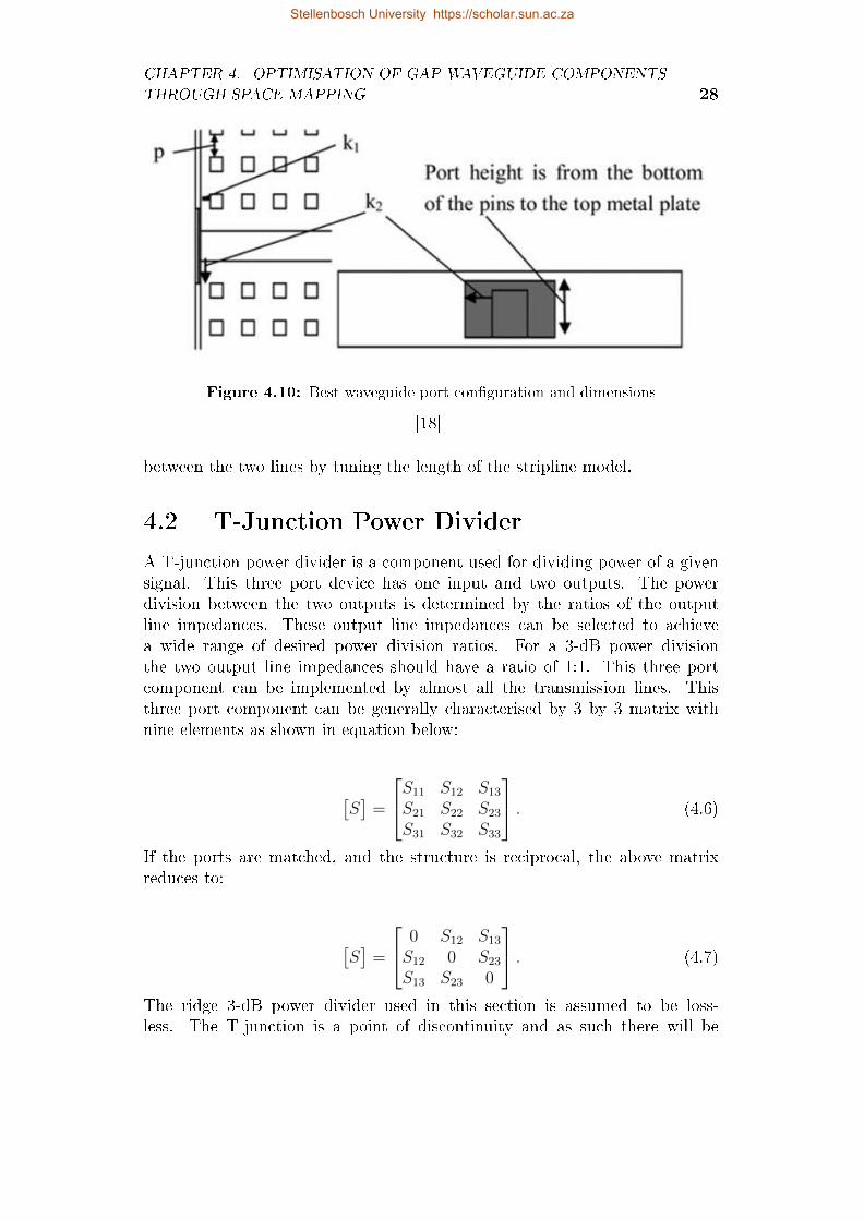
The parameter p is the inter pin distance, k2 is distance from ridge wallto the rst pin wall or waveguide port edge which is equal to p in this case,k1 is the distance from the last pin edge end to bottom or upper plate endsas shown in the Fig. 4.10 and it was found to be p
2. This waveguide port
location, conguration and dimensions was found to give best results for bothgroove and ridge gap waveguides.
In summary, the equivalence between ridge/groove gap waveguides andridge/rectangular waveguides was established through plots of dipersiongraphs. The study of waveguide ports dimensions and conguration [25] has
Stellenbosch University https://scholar.sun.ac.za

CHAPTER 4. OPTIMISATION OF GAP WAVEGUIDE COMPONENTS
THROUGH SPACE MAPPING 26
Figure 4.6: Ridge gap/ridged rectangular waveguides dispersion graphs for h = 2
Figure 4.7: Ridge gap/ridged rectangular waveguides dispersion graphs for h = 3
shown the best waveguide ports dimensions and conguration for simulationof gap waveguide structures. Using their geometrical resemblance, the ridgedand hollow rectangular waveguide geometry can be used as a starting geome-try in the design of ridge and groove gap waveguide components respectively.The already known ridged rectangular waveguide formulas can be used tocalculate the corresponding parameters of the ridge gap waveguide because oftheir equivalence.
The dispersion plots of the ridge gap waveguide also showed the limitationof using the stripline model for large vacuum gap height to ridge width ratios inthe ridge gap waveguide. The propagation constant of the ridge gap waveguideTEM mode decreased as the ratio increased. This meant that the wavelengthof the ridge gap waveguide TEM mode increased. However, we choose and use
Stellenbosch University https://scholar.sun.ac.za

CHAPTER 4. OPTIMISATION OF GAP WAVEGUIDE COMPONENTS
THROUGH SPACE MAPPING 27
Figure 4.8: Groove/hollow waveguide dispersion graphs
Figure 4.9: (a) Groove waveguide port arrangement and (b )ridge waveguide portarrangement
[18]
the shorter wavelength vacuum TEM stripline to model a ridge gap waveguideTEM line which has a longer wavelength. We correct or reduce the error
Stellenbosch University https://scholar.sun.ac.za
CHAPTER 4. OPTIMISATION OF GAP WAVEGUIDE COMPONENTS
THROUGH SPACE MAPPING 28
Figure 4.10: Best waveguide port conguration and dimensions
[18]
between the two lines by tuning the length of the stripline model.
4.2 T-Junction Power Divider
A T-junction power divider is a component used for dividing power of a givensignal. This three port device has one input and two outputs. The powerdivision between the two outputs is determined by the ratios of the outputline impedances. These output line impedances can be selected to achievea wide range of desired power division ratios. For a 3-dB power divisionthe two output line impedances should have a ratio of 1:1. This three portcomponent can be implemented by almost all the transmission lines. Thisthree port component can be generally characterised by 3 by 3 matrix withnine elements as shown in equation below:
[S]
=
S11 S12 S13
S21 S22 S23
S31 S32 S33
. (4.6)
If the ports are matched, and the structure is reciprocal, the above matrixreduces to:
[S]
=
0 S12 S13
S12 0 S23
S13 S23 0
. (4.7)
The ridge 3-dB power divider used in this section is assumed to be loss-less. The T-junction is a point of discontinuity and as such there will be
Stellenbosch University https://scholar.sun.ac.za

CHAPTER 4. OPTIMISATION OF GAP WAVEGUIDE COMPONENTS
THROUGH SPACE MAPPING 29
fringing elds and higher order modes [24] in the junction. This results instored energy in the junction which is modelled by susceptance jB in Fig. 4.11.
Figure 4.11: Transmission line model of a power divider
[24]
From Fig. 4.11 any of the three T-junction power divider impedance linesZo, Z1 and Z2 can be used as an input port with output power being dividedbetween the remaining two output ports. The eective load impedance of thefeed port seen at the junction is the parallel impedance combination of theother two ports, if there are terminated in their characteristic impedances.
4.3 Optimisation of 3-dB Ridge Gap
Waveguide T-Junction Power Divider
Using Input Space Mapping
A waveguide power divider with a characteristic impedance of 50 Ω in [4]was designed and optimised using space mapping. A 50 Ω stripline wasused to coarse model the ridge gap waveguide power divider. The striplineequations were used to calculate the ridge width of the ridge gap waveguide.The characteristic impedance formula of the ridged waveguide was used tocalculate the vacuum gap height h of the ridge gap waveguide ne model.
As already stated in the previous section for a 50 Ω power divider, anychosen input port in the T-power divider will be loaded by an eective loadof two parallel 50 Ω impedances of the other two ports. The eective load atthe T-junction seen by the feed port will be thus be 25 Ω. This implies thatthere will be a mismatch between 50 Ω input port and the 25 Ω eective loadimpedance seen at the junction. For this reason a quarter wave transformer
Stellenbosch University https://scholar.sun.ac.za
CHAPTER 4. OPTIMISATION OF GAP WAVEGUIDE COMPONENTS
THROUGH SPACE MAPPING 30
needs to be inserted between the 50 Ω input port and the 25 Ω T-junctionload for matching. The characteristic impedance of the matching quarterwave transformer was calculated as follows:
Zquarter wave =√
(50 ∗ 25) = 35.4 Ω. (4.8)
The width of quarter wavelength line w2 was calculated using (4.4) and (4.5)for a pre-selected stripline height of 2 mm and its value is 7.12 mm.
The width of the stripline coarse model w1 was calculated using (4.4)and (4.5) for a pre-selected stripline height of 2 mm and a 50 Ω impedance.The calculated width value is 2.87 mm. The calculated strip width of thestripline coarse model was also used as the width of the ridge gap waveguidene model. There were two options for the coarse model. The rst optionwas to use the same width and height for both coarse and ne models and a25 Ω impedance from (4.1). The second option was to use similar widths andimpedances of 50 Ω for both coarse and ne models and have the height ofthe stripline as a variable for the correct impedance. Both options were tried.The rst option did not work, it gave a totally wrong coarse model response.The second option worked well giving the expected response.
In the example [4], it was not clearly stated by the author which of thetwo options stated above works when using a stripline to model a ridge gapwaveguide. Generally, in using the stripline to model a ridge gap waveguide,the widths and impedances of the two models should be the same and theheight should be the variable to get the right impedance.
The schematic diagram of the stripline model is shown in Fig. 4.12with the matching transformer length shown as L2 and its width as w2.The length of the stripline is L1 and its width is w1. The length of thetransformer L2 and L1 were chosen as design parameters because of reasonsstated in subsection 4.1.2. The power divider was designed for a centrefrequency of 15 GHz. The calculated quarter wavelength at this frequencyis 5 mm. This length of the lines was scaled to 3λ
4which is 15 mm to
accommodate two rows of pins in the ne model. The coarse model was sim-ulated using MWO. The optimum coarse model response is shown in Fig. 4.13.
The 3-D ne model of the power divider is shown in Fig. 4.14. Thecalculated stripline width of the coarse model was used as the ridge widthas well in the ne model. From the equivalence of ridged rectangularwaveguide and ridge gap waveguide discussed in the above subsection 4.1.2,the characteristic impedance formula of the former was used to approximatethe ridge gap waveguide vacuum height gap h for a characteristic impedace of
Stellenbosch University https://scholar.sun.ac.za

CHAPTER 4. OPTIMISATION OF GAP WAVEGUIDE COMPONENTS
THROUGH SPACE MAPPING 31
Figure 4.12: MWO stripline coarse model schematic
Figure 4.13: MWO stripline coarse model response
50 Ω [26]. The characteristic impedance formula is:
Z0 = Z0∞[1− (λ/λcr)
2]−1/2 (4.9)
where Z0∞ is the characteristic impedance for innity frequency and is givenby:
Stellenbosch University https://scholar.sun.ac.za

CHAPTER 4. OPTIMISATION OF GAP WAVEGUIDE COMPONENTS
THROUGH SPACE MAPPING 32
Figure 4.14: CST 3-D ne model diagram
Z0∞ =120π2 (b/λcr)
bd
sin π sbbλcr
+[B0
Y0+ tan π
2bλcr
(a−sb
)]cos π s
bbλcr
(4.10)
and λcr is given by:
b
λcr=
b
2(a− s)
[1 +
4
π
(1 + 0.2
√b
a− s
)b
a− sln csc
π
2
d
b
+(
2.45 + 0.2s
a
) sb
d(a− s)
]−1/2(4.11)
where λcr is the waveguide cut-o wavelength. The cross sectional dimensionsand parameters a, b, d and s of both double and single ridge waveguides areshown in Figs. 4.15 (a) and (b). It should be noted that (4.10) and (4.11)were derived using double ridged waveguide with b and d values being twicethose of a single ridged waveguide. In this example a single ridged waveguidewas used for the power divider. Hence to get the correct characteristicimpedance formulas, the double ridged waveguide formulas (4.10) and (4.11)were divided by 2.
Stellenbosch University https://scholar.sun.ac.za

CHAPTER 4. OPTIMISATION OF GAP WAVEGUIDE COMPONENTS
THROUGH SPACE MAPPING 33
Figure 4.15: Cross sectional dimensions of double and single ridged waveguides
The above equations were implemented in MATLAB to calculate theridge gap height h for an impedance of 50 Ω. The calculated value of hwas 0.66 mm. This vacuum gap height value was used in the ridge gapwaveguide ne model. The 3-dB ridge gap waveguide power divider wasoptimised using an in-house input space mapping code. The design goaltype of the code is |S11| and the design specication is given as a [14 -15] GHz frequency range for a level of -15 dB. The results of the rstiteration in which the ne model was evaluated using the calculated pa-rameter values did not meet the design specications and is shown in Fig. 4.16.
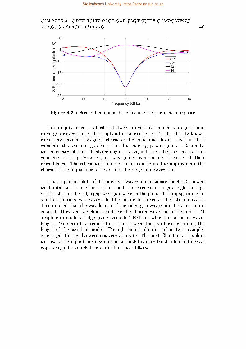
Using the design parameters, the stripline coarse model response wasmapped and aligned to the ne model response which resulted in an alignedsurrogate model. The aligned surrogate model was optimised to get newdesign parameter values in the second iteration for evaluation of the nemodel. The evaluated ne model response in the second iteration using thenew design parameter values is shown in Fig. 4.17. The ne model responsefor the second iteration was within the acceptable design specicationaccuracy range. The design specication was thus met in just two spacemapping iterations of evaluating the ne model.
Stellenbosch University https://scholar.sun.ac.za

CHAPTER 4. OPTIMISATION OF GAP WAVEGUIDE COMPONENTS
THROUGH SPACE MAPPING 34
Figure 4.16: CST ne model rst iteration
4.4 Design and Optimisation of a 3-dB Ridge
Gap Waveguide Hybrid Coupler Using
Input Space Mapping
A 3-dB ridge gap waveguide hybrid coupler was designed and optimised usinginput space mapping. The input space mapping procedure and steps have al-ready been discussed in Chapter 3. In this design example the space mappingsteps were manually done as the in-house input space mapping code did not yethave the ability to simultaneously handle multiple design responses of interest.
A 3-dB quadrature hybrid coupler is a four port network with outputpower being equally divided between through and coupled ports. The porton the same side as the input port is the isolated port and ideally it has nopower coupled to it. The coupled and through ports are on the opposite sideof the input port. The output of the through and coupled ports have a phasedierence of 90o. The schematic diagram of a hybrid coupler with typicalport conguration is shown in Fig. 4.18. Two sets of quarter wavelengthlines are used in the coupler and these are shown in the schematic as seriesand parallel. The characteristic impedance of the series quarter wavelength
Stellenbosch University https://scholar.sun.ac.za

CHAPTER 4. OPTIMISATION OF GAP WAVEGUIDE COMPONENTS
THROUGH SPACE MAPPING 35
Figure 4.17: CST ne model second iteration
lines is Zo/√
2 where Zo is the characteristic impedance of the coupler. Thecharacteristic impedance of the parallel quarter wavelength lines is Zo. Itshould be noted that the hybrid coupler is symmetric and as such any portcan be used as an input port.
The operation of the hybrid can be analysed using even-odd mode cong-uration analysis. The hybrid is fully characterised by a 4 by 4 symmetricalmatrix [24] given by:
[S]
=−1√
2
0 j 1 0j 0 0 11 0 0 j0 1 j 0
. (4.12)
The above matrix show all the possible output lines power ratios for anyof the 4 ports used as input. Each column in the matrix corresponds to the4 possible input ports. For example column 3 of the matrix is a summaryof output power ratios when port 3 is used as an input port. With matched
Stellenbosch University https://scholar.sun.ac.za

CHAPTER 4. OPTIMISATION OF GAP WAVEGUIDE COMPONENTS
THROUGH SPACE MAPPING 36
Figure 4.18: Hybrid coupler schematic diagram
port 3 as the input port, the power coupled to port 2 is zero, half power iscoupled to port 1 with a phase shift of −180o from port 3 to 1 and half poweris coupled to port 4 with a phase shift of −90o from port 3 to 4. The powerphase dierence between the through and coupled ports is 90o. A 3-dB hybridcoupler was designed using input space mapping for centre frequency of 15GHz with a characteristic impedance of 50 Ω.
The stripline coarse model was used in this example. The stripline coarsemodel dimensions used are similar to those used in the previous example.Like in the previous example, the initial length of quarter wavelength lines is5 mm and this was scaled up to 3λ
4so as to accommodate enough pin rows
in the central region of coupler ne model. MWO was used to simulate thestripline model. The schematic diagram of the stripline coarse model is shownin Fig. 4.19.
The design parameters are shown in Fig. 4.19. There are series 35.4 Ωquarter wavelength transformers line lengths shown as L2, a 50 Ω quarterwavelength parallel line lengths shown as L1 and their width shown as w1.The four terminal lines had their width and lengths xed for matching with50 Ω feed ports. The widths of the quarter wavelength transformers werecalculated using (4.4) and (4.5). The calculated width of the 35.4 Ω line whichis 4.42 mm, could not be used as a design variable because of the limited
Stellenbosch University https://scholar.sun.ac.za

CHAPTER 4. OPTIMISATION OF GAP WAVEGUIDE COMPONENTS
THROUGH SPACE MAPPING 37
Design Variables Surrogate (Rs) Coarse (Rc) Parameter C
W1 0.39 2.87 −2.48L1 13.24 15 −2.76L2 14.11 15 −0.89
Table 4.1: Alignment step
middle region pin space in the ne model. Hence this width was xed. Thethree design variables are L1, L2 and w1.
Figure 4.19: MWO coupler coarse model schematic diagram
The stripline coarse model was evaluated using the initial calculatedparameter values and its optimum S-parameter response is shown Fig. 4.20.The ne model was simulated in CST. The CST 3-D ne model and thedesign parameters are shown in Fig. 4.21. The dimensions of the ne modelare pin height d of 5 mm, vacuum gap height h of 0.66 mm, pin width a of2.5 mm and the distance between the pins p of 4 mm. The hybrid couplerne model was evaluated using the initial calculated parameter values and itsinitial S-parameter response is shown in Fig. 4.22.
The ne model response is o the design specication as seen in Fig. 4.22.The next step was to align the coarse and ne models. The three designparameters were used to align the coarse and ne models. This alignment stepis summarised in Table 4.1. The coarse model, ne model and the alignedsurrogate model are shown in Fig. 4.23.
Stellenbosch University https://scholar.sun.ac.za

CHAPTER 4. OPTIMISATION OF GAP WAVEGUIDE COMPONENTS
THROUGH SPACE MAPPING 38
Figure 4.20: MWO coupler coarse model S-parameters
Figure 4.21: CST coupler 3-D ne model
The resultant aligned surrogate model was optimised for new coarse modeldesign values. This optimisation step was redundant in this example becauseby design the coarse model was optimum. The new design values from (3.6)are shown in Table 4.2. These were used to evaluate the hybrid coupler nemodel. The response of the ne model is shown in Fig. 4.24. With onemanual iteration of input space mapping involving evaluation of ne model2 times, a nearly optimum hybrid coupler was designed for 15 GHz centrefrequency.
The results of the 3-dB ridge gap waveguide power divider and hybrid
Stellenbosch University https://scholar.sun.ac.za

CHAPTER 4. OPTIMISATION OF GAP WAVEGUIDE COMPONENTS
THROUGH SPACE MAPPING 39
Figure 4.22: CST coupler ne model initial S-parameters
Figure 4.23: Alignment step and the aligned models
Design Variables Surrogate (Rs) New values (Rc) Parameters C
W2 2.87 5.35 −2.48L1 15 17.76 −2.76L2 15 15.89 −0.89
Table 4.2: New coarse model design values
coupler generally show that using the calculated design parameter values indesign, in most cases do not give an optimum design. The design parametersneed to be tuned or optimised to meet the design specications. The ex-amples also showed the eciency of the space mapping optimisation technique.
Stellenbosch University https://scholar.sun.ac.za
CHAPTER 4. OPTIMISATION OF GAP WAVEGUIDE COMPONENTS
THROUGH SPACE MAPPING 40
Figure 4.24: Second iteration and the ne model S-parameters response
From equivalence established between ridged rectangular waveguide andridge gap waveguide in the stopband in subsection 4.1.2, the already knownridged rectangular waveguide characteristic impedance formula was used tocalculate the vacuum gap height of the ridge gap waveguide. Generally,the geometry of the ridged/rectangular waveguides can be used as startinggeometry of ridge/groove gap waveguides components because of theirresemblance. The relevant stripline formulas can be used to approximate thecharacteristic impedance and width of the ridge gap waveguide.
The dispersion plots of the ridge gap waveguide in subsection 4.1.2, showedthe limitation of using the stripline model for large vacuum gap height to ridgewidth ratios in the ridge gap waveguide. From the plots, the propagation con-stant of the ridge gap waveguide TEM mode decreased as the ratio increased.This implied that the wavelength of the ridge gap waveguide TEM mode in-creased. However, we choose and use the shorter wavelength vacuum TEMstripline to model a ridge gap waveguide TEM line which has a longer wave-length. We correct or reduce the error between the two lines by tuning thelength of the stripline model. Though the stripline model in two examplesconverged, the results were not very accurate. The next Chapter will explorethe use of a simple transmission line to model narrow band ridge and groovegap waveguides coupled resonator bandpass lters.
Stellenbosch University https://scholar.sun.ac.za

Chapter 5
Optimisation of Microwave Gap
Waveguide Bandpass Filters Using
Space Mapping
5.1 Bandpass Filter Basics
A bandpass lter is a two port electronic circuit that allows transmission ofa given band of frequencies but rejects the frequencies outside the passband.Bandpass lters are mostly fabricated using lumped elements (resistor, induc-tor and capacitor), distributed elements(transmission lines) and waveguides.The atness of the transmission function response in the passband and thesharpness of its transition from passband frequency edge to stopband fre-quency edge, called selectivity factor, is one of the lter design considerations.Generally transmission ripples are not desirable in the passband, but lowervalues of less than 1 dB are acceptable in most bandpass lter applications.In some applications, the sharpness of the transition cut-o response frompassband frequency edge to stopband frequency edge is more important thanits atness in the passband and this depends on the selectivity factor of thelter.
The selectivity factor is the ratio of stopband edge frequency(ωs) topassband edge frequency (ωp) which is a measure of sharpness, steepness orroll-o between the two frequencies. The two frequency edges of a bandpasslter ωp and ωs and the transition band are shown in Fig. 5.1(a). Ideally thereshould be zero transition band between the two cut-o frequency edges orselectivity factor of 1. Increasing selectivity factor or improving the sharpnessof the cut-o response results in ripples in the transmission function responsein the passband. Filters whose transmission function have equal ripples in thepassband and monotonically decreasing in the stopband are called Chebyshevlters. The bandpass lter designs in this chapter are based on Chebyshev
41
Stellenbosch University https://scholar.sun.ac.za

CHAPTER 5. OPTIMISATION OF MICROWAVE GAP WAVEGUIDE
BANDPASS FILTERS USING SPACE MAPPING 42
type I (rst kind) lter whose transmission function has ripples only in thepassband but none in the stopband. Typical Chebychev bandpass ltertransmission function responses for an even (N = 4) and odd (N = 5) orderChebyshev type I lter are shown in Fig. 5.1.
Figure 5.1: Chebyshev transmission function response
5.1.1 Chebyshev Bandpass Filter Transfer Function
As already stated, a Chebychev type I bandpass lter is characterized by atransmission function with equal ripples in the passband and monotonicallydecreasing in the stopband with no ripples in the stopband. The order of thelter (number of poles) is indicated by the number of transmission functionmaxima and minima (poles) in the passband. For a Chebyshev type I, thetransmission zeros are at ω = ∞, hence it is called an all pole lter. Thetransfer function of an N th order Chebyshev lter with its magnitude squaredis:
|S21(jω)|2 =1
1 + ε2T 2N(ω)
(5.1)
where TN(ω) is the N th Chebyshev polynomial dened in the following rangesas:
TN(ω) = cos(N cos−1 ω) for |ω|≤1
Stellenbosch University https://scholar.sun.ac.za

CHAPTER 5. OPTIMISATION OF MICROWAVE GAP WAVEGUIDE
BANDPASS FILTERS USING SPACE MAPPING 43
TN(ω) = cosh(N cosh−1 ω) for |ω|>1.
The magnitude of the transmission function at passband frequency edgeω = ωp is:
|S21(jω)| = 1√1 + ε2
(5.2)
where ε is the ripple constant related to the specied bandpass ripple level(Ar)by:
Ar = 10 log(1 + ε2). (5.3)
Solving for ripple constant (ε) gives
ε =√
10Ar/10 − 1. (5.4)
The Chebyshev polynomials may be generated recursively using:
T0(ω) = 1 (5.5)
T1(ω) = ω (5.6)
TN+1(ω) = 2(ω)TN(ω)− TN−1(ω). (5.7)
5.1.2 Chebyshev Lowpass Filter prototype ElementValues
Like other types of lters, the design and realisation of actual Chebyshevbandpass lter is based on the normalized lowpass lter prototype elementvalues. The lowpass lter prototype element values are impedance andfrequency scaled for realisation of the actual bandpass lter. The Chebyshevlowpass lter prototype element values are calculated from the lumpedelement lowpass lter prototype circuit shown in Fig. 5.2.
The calculated element values depend on the specied passband ripplelevel (Ar). The value of the normalized source impedance is given by g0 = 1.The load impedance (r) value depends on the order of the lter N and r = 1for N odd and r = coth2(β
4) for N even. The other element values are given by:
Stellenbosch University https://scholar.sun.ac.za

CHAPTER 5. OPTIMISATION OF MICROWAVE GAP WAVEGUIDE
BANDPASS FILTERS USING SPACE MAPPING 44
Figure 5.2: Lumped element lowpass lter circuit
g1 =2a1γ
(5.8)
gk =4ak−1akbk−1gk−1
for k = 2, 3, ...N (5.9)
where
ak = sin
[(2k − 1)π
2N
]for k = 1, 2, ...N (5.10)
bk = γ2 + sin2
(kπ
N
)for k = 1, 2, ...N (5.11)
β = ln
(coth
Ar17.37
)where Ar is ripple level in dB (5.12)
γ = sinh
(β
2N
). (5.13)
5.1.3 Narrow Band Coupled Resonator BandpassFilters
At microwave frequencies narrow band bandpass lters are often realised fromhigh-quality factor (high-Q) resonant ciruits or cavitives loosely coupled toeach other in cascade. At this frequency range, the resonators are usuallyrealised from transmission lines and rectangular waveguides. The selectivityfactor or steepness of cuto between passband fequency edge and stopbandfrequency edge increases as the number of resonators are increased [27]. Thenumber of resonators also determine the order of the lter. The couplingbetween adjacent resonators can either be inductive (impedance inverter) orcapacitive (admittance inverter). The external quality factor Qex of the rstand last resonators, in the lter resonator cascade arrangement, is lowered
Stellenbosch University https://scholar.sun.ac.za

CHAPTER 5. OPTIMISATION OF MICROWAVE GAP WAVEGUIDE
BANDPASS FILTERS USING SPACE MAPPING 45
because of the source and load impedances loading of the respective resonators.
All types of narrow band bandpass coupled resonator lters are basicallycharacterized by three parameters. These are the synchronous tuningfrequency of each resonator, main line coupling between adjacent resonatorsand the external quality factor Qex of the rst and last resonators [28]. Animpedance inverter K coupling model will be discussed and used in thischapter. An impedance inverter K model for Chebyshev bandpass lter isshown in Fig. 5.3. There are several lumped element equivalent circuits forthe impedance inverter K. A typical T-lumped element equivalent circuitof a impedance inverter K is shown in Fig. 5.4. The value of the couplingfactor K between two adjacent resonators can be calculated from the resonantfrequencies of each resonator and this will be discussed in detail in the nextsubsection. The value of main line coupling factor K can also be calculatedfrom the relevant lowpass lter prototype element values using:
Ki,i+1 =πBW
2√gi.gi+1
for i = 1 to (N − 1) (5.14)
where BW is the lter relative bandwidth and N is the number of resonators[29].
Figure 5.3: Impedance Inverter model for Chebyshev bandpass lter
Figure 5.4: K-Inverter equivalent lumped elements circuit
The external quality factor value Qex of the rst and last resonators canalso be calculated from lowpass lter prototype element values using (5.15)
Stellenbosch University https://scholar.sun.ac.za

CHAPTER 5. OPTIMISATION OF MICROWAVE GAP WAVEGUIDE
BANDPASS FILTERS USING SPACE MAPPING 46
and (5.16). The external quality factor Qex can also be expressed in terms ofcoupling between the feed port and the rst resonator using (5.17).
Qex1 =2g0g1πBW
for rst resonator (5.15)
QexN =2gN .gN+1
πBWfor last resonator (5.16)
K01
Zo=
√π
2Qex
(5.17)
5.1.4 Calculation of Coupling Factor K Using ElectricWall Magnetic and Wall Symmetry
The coupling factor K between two adjacent resonators can be calculatedfrom their respective resonant frequencies. The circuit model of two adjacentcoupled resonators is shown in Fig. 5.5 (a).
Figure 5.5: Electric wall and magnetic wall symmetry method
Stellenbosch University https://scholar.sun.ac.za

CHAPTER 5. OPTIMISATION OF MICROWAVE GAP WAVEGUIDE
BANDPASS FILTERS USING SPACE MAPPING 47
Using the electric wall and magnetic wall symmetry method (even andmode analysis), the two resonators in the circuit model can be divided intosingle resonators with an electric and magnetic wall terminations. Thesymmetrical mutual inductive coupling M between the two resonators shownin Fig. 5.5 (a), can be broken down into an equivalent circuit shown inFig. 5.5 (b). The mutual coupling equivalent circuit of Fig. 5.5 (b) is aT-impedance inverter K with two series inductors −Lm and a shunt inductorLm and is similar to the one shown in Fig. 5.4. The circuit of Fig. 5.5 (b) canbe further broken down into two separate resonators of even and odd modes.The even mode resonator 1 is terminated with a magnetic wall, which is anopen circuit termination as shown in Fig. 5.5(c). The odd mode resonator2 is terminated with an electric wall, which is a short circuit termination asshown in Fig. 5.5(d). The odd and even mode resonant frequencies of thetwo individual resonator circuits are calculated using (5.18) and (5.19). Theinductive coupling factor KM between the two resonators is solved from (5.18)and (5.19) and is given by (5.20):
fm =1
2π√
(L+ Lm)C(5.18)
fe =1
2π√
(L− Lm)C(5.19)
KM =LmL
=f 2e − f 2
m
f 2e + f 2
m
. (5.20)
Equation (5.20) will be used in the practical analysis and calculation of cou-pling factor K and the related distance s between two groove gap waveguideresonators in the following sections.
The calculated values of coupling factor K and the the external qualityfactor Qex are electrical parameters. The two parameters need to be translatedinto physical dimensions for the realisation of actual bandpass lters. Thevalue of K needs to be translated into some physical dimension relating tothe two adjacent resonators. The value of Qex needs to be translated intosome physical dimension relating the source and rst resonator and as alreadystated this will also apply to the last resonator and its load in all the lterexamples discussed in this chapter.
The next section will look at narrow band microwave groove gap waveguidecoupled resonator bandpass lters. The main line coupling factor K andthe external quality external factor Qex which are electrical parameters, willbe translated into physical dimensions. The methods for calculation andpractical realization of K and Qex values will be discussed. It should be noted
Stellenbosch University https://scholar.sun.ac.za
CHAPTER 5. OPTIMISATION OF MICROWAVE GAP WAVEGUIDE
BANDPASS FILTERS USING SPACE MAPPING 48
that although the groove gap waveguide resonators were used for calculationand analysis of the two parameters, the methods and procedure generallyapply to other types of coupled resonator bandpass lters as well.
5.2 Narrow Band Microwave Groove Gap
Waveguide Coupled Resonator Bandpass
Filters
Third and fth order narrow band microwave groove gap waveguide bandpasslter examples [5] using high Q groove gap waveguide resonators were done.The groove gap waveguide resonators and lter dimensions from [5] wereused. The lters were realised from cascaded groove gap waveguide resonatorswhich were loosely coupled. The coupling factor K and the physical distances between two adjacent groove gap waveguide resonators was analysed andcalculated using the S-parameter and eigenmode solver methods. The externalquality factor Qex of the typical rst groove gap waveguide resonator andthe source SMA port position x was calculated and analysed using the groupdelay method.
5.2.1 Practical Realisation of Coupling Factor K UsingS-Parameter Method
The S-parameters S11 and S21 of two adjacent resonators were used in theanalysis of coupling factor K between the two adjacent groove gap waveguideresonators seperated by distance s. The two resonator arrangement withsymmetrical ports separated by a distance s =1.5 mm is shown in Fig. 5.6.The initial value of s was arbitrary as any other reasonable value couldhave been used. Standard Ku band dimensions of the conventional hollowrectangular waveguide [5] with a width of 15.mm and a length of 15.6 mm wereused for the resonators. The other dimensions of the groove gap waveguideresonators were pins of width a = 1 mm, pin height d = 6.25 mm, distancebetween pins period p = 3 mm, vacuum gap height h= 1 mm. The dimensionswere for the intended 10 - 20 GHz stopband of the groove gap waveguidebandpass lters.
The resonator arrangement was simulated as a two port network for S11
and S21 using CST. For the S-parameter method to work, the two resonatorswere weakly coupled to their respective ports [29]. The two resonators wereweakly coupled to their ports by reducing the SMA port inner probe lengthinto the resonators. The SMA ports were placed on the upper PEC plate
Stellenbosch University https://scholar.sun.ac.za

CHAPTER 5. OPTIMISATION OF MICROWAVE GAP WAVEGUIDE
BANDPASS FILTERS USING SPACE MAPPING 49
Figure 5.6: Two resonator arrangement for the S-parameter method
which is 1 mm above the resonator pins with inner probes of the portsextending into the resonator cavities. The upper PEC plate is not shown inFig. 5.6 for clarity. Two troughs for the simulated S11 and S21 parameterswere observed. The two troughs correspond to the resonant frequency of eachresonator. The distance between the two resonators s was varied and thetroughs were observed to be shifting in line with s variation. The resonancetroughs and their corresponding resonant frequencies are shown in Fig. 5.7.
Figure 5.7: Main-line coupling S-parameters
The two S11 resonance trough frequencies were used to calculate the
Stellenbosch University https://scholar.sun.ac.za

CHAPTER 5. OPTIMISATION OF MICROWAVE GAP WAVEGUIDE
BANDPASS FILTERS USING SPACE MAPPING 50
s 0 0.5 1 1.5 2 2.5 2.75 3
K 0.0024 0.014 0.009 0.0058 0.004 0.0037 0.0034 0.003
Table 5.1: Coupling K and corresponding inter-resonator distance s
coupling K between the two resonators using (5.20) for inter-resonatordistance s = 1.5 mm. The calculated value was K = 0.0057. This then wasthe coupling factor K value between the two resonators for the particularinter-resonator separation distance of s = 1.5 mm. Evenly spaced samplevalues of s in the range [0 - 3] mm were used for S11 simulation and theresultant resonant frequencies values were used to calculate the correspondingvalues of K using (5.20). The calculated values of K and the correspondingdistances s values were tabulated and are shown in Table 5.1.
Using the results of Table 5.1, an approximated graph of main-linecoupling factor K and the corresponding inter-resonator separation distances was plotted and is shown in Fig. 5.8. The graph shows the physicalrelationship between the electrical parameter K and the correspondingphysical inter-resonator-distances s.
Figure 5.8: Approximated graph of K and inter-resonator distance s (mm)
5.2.2 Practical Realisation of Coupling Factor K UsingEigenmode Method
The second eigenmode solver method was used to calculate and analyse thecoupling factor K between two groove gap waveguide resonators which were
Stellenbosch University https://scholar.sun.ac.za

CHAPTER 5. OPTIMISATION OF MICROWAVE GAP WAVEGUIDE
BANDPASS FILTERS USING SPACE MAPPING 51
placed next to each other separated by distance s. The analysis was doneusing the CST eigenmode solver option. The dimensions of the groove gapwaveguide resonators used in the analysis were similar to those used in theS-parameter method. The two adjacent resonators were separated by distances = 1.5 mm. The initial value of s was arbitrary as any other reasonable valuecould have been used. The two resonator arrangement is shown in Fig. 5.9.
Figure 5.9: Eiegemmode solver method
The resonator arrangement was simulated using CST eigenmode solver fortwo modes. Two resultant resonant frequencies for each mode were observed.These were the resonant frequencies of each resonator in the simulatedarrangement. The two frequencies were post processed using the CST postprocessing results template. The post processing of the two frequencies wasbased on (5.20). For the inter-resonator separation distance s = 1.5 mm,the template calculated a value of K = 0.0055. This then was the couplingfactor K value between the two groove gap waveguide resonators for theparticular separation distance s = 1.5 mm. A parameter sweep of distances was done in the [0 - 3] mm range to for calculation and plotting of valuesof K and the corresponding s values in CST. The resultant graphs of Kas a function of s and all the post processed results are shown in Figs. 5.10 - 12.
The graph of Fig. 5.12 shows the general relationship between couplingfactor K and the corresponding variation of distance s between two resonators.A MATLAB code was written to approximate the best t function for theeigenmode solver resultant function of Fig. 5.12. The non-smooth andnon-linear behaviour of K as a function s graph was approximated by thebest t function to get a closed form functional relationship between thedistance s and the coupling factor K. The tting function is monotonic and
Stellenbosch University https://scholar.sun.ac.za

CHAPTER 5. OPTIMISATION OF MICROWAVE GAP WAVEGUIDE
BANDPASS FILTERS USING SPACE MAPPING 52
Figure 5.10: Mode 1
Figure 5.11: Mode 2
it mathematically entails the simple, but non-linear relationship betweens and coupling factor K which is good for the space mapping. We cantherefore encode the complex non-linear behaviour of K as a function ofs into our coarse model. The best t function is also shown in Fig. 5.12.The S-parameter method sample values were also plotted in Fig. 5.12 forcomparison. The two methods gave similar results. The approximated bestt function is:
Ks =as
100(s+ cs)
−bs (5.21)
where a, b and c are the tting constants.
Stellenbosch University https://scholar.sun.ac.za

CHAPTER 5. OPTIMISATION OF MICROWAVE GAP WAVEGUIDE
BANDPASS FILTERS USING SPACE MAPPING 53
Figure 5.12: Eigenmode solver method for K and s
5.2.3 Calculation and Realisation of The ExternalQuality Factor Qex Using Group Delay Method
The group delay method was used to analyse the relationship between externalquality factor Qex of a typical rst groove gap waveguide resonator and theSMA port feed point x. The 3-D model of the groove gap waveguide resonatorand SMA port feed position x used in the analysis is shown in Fig. 5.13. Thedimensions of the groove gap waveguide resonator are similar to those used inthe S-parameter and eigenmode solver methods. The SMA port inner probedepth into the resonator was kept constant at 2 mm. The simulation set-upis fully discussed later in the section.
The group delay method is based on the group delay of the reectioncoecient S11 phase in a typical source and rst resonator arrangement. Thecircuit model of the typical rst resonator and source arrangement is shown inFig. 5.14. Without the source, the resonator in the circuit model has innitequality factor Q - that is there is only stored energy and no dissipated energy.The source port in the circuit model of Fig. 5.14 loads the resonator with alossy component (the port impedance). The external quality factor Qex of theloaded resonator goes down since Q =(stored energy)/(dissipated energy).
The reection coecient S11 of the circuit model feed line of input admit-tance G loaded by the resonator (L-C) as shown in Fig. 5.14 is:
S11 =G− YinG+ Yin
=1− Yin
G
1 + YinG
(5.22)
with impedance seen into the resonator as :
Stellenbosch University https://scholar.sun.ac.za

CHAPTER 5. OPTIMISATION OF MICROWAVE GAP WAVEGUIDE
BANDPASS FILTERS USING SPACE MAPPING 54
Figure 5.13: Group delay method with resonator and SMA port distance x
Figure 5.14: Typical circuit model of source and rst resonator
Yin = jωC +1
jωL= jω0
(ω
ω0
− ω0
ω
)(5.23)
where resonance frequency ω0 = 1√LC
. For frequencies near resonance, ω = ωo+ ∆ω, where ∆ω ωo and (5.23) can be approximated by:
Yin ≈ jω0C2∆ω
ω0
(5.24)
where ∆ω is the small frequency deviation from resonant frequency. Substi-tuting (5.24) into (5.22), the reection coecient S11 can be re-written as:
S11 =1− jQex (2∆ω/ω0)
1 + jQex (2∆ω/ω0)(5.25)
Stellenbosch University https://scholar.sun.ac.za
CHAPTER 5. OPTIMISATION OF MICROWAVE GAP WAVEGUIDE
BANDPASS FILTERS USING SPACE MAPPING 55
where the external quality factor Qex = (ω0C/G). Equation(5.25) can bere-written in polar form as :
S11 =
∣∣∣∣1− jQex (2∆ω/ω0)
1 + jQex (2∆ω/ω0)
∣∣∣∣ 6 ϕ (5.26)
where the reection phase angle ϕ is given by:
ϕ = −2 arctan
(2Qex
(2
(ω − ω0)
ω0
)). (5.27)
The group delay (τ) is the derivative of the reection coecient S11 phaseangle ϕ with respect to the angular frequency. Generally, it is a measureof the distortion in the signal introduced by phase dierences for dierentfrequencies. The group delay is the slope of the graph of S11 (phase) as afunction of frequency and is given by:
τ = −δϕδω
(5.28)
τ =4Qex
ω0
1
1 + (2Qex (ω − ω0/ω0))2 . (5.29)
Equation (5.29) gives the general group delay as a function of frequency.For convenience and simplicity we select the resonant frequency becauseit simplies (5.29) and is easy to identify the resulting graph of the groupdelay. The group delay τmax is maximum at resonance where ω = ωo, and theexternal quality factor Qex at resonance from (5.29) is:
Qex =2πf0τmax
4=πf0τmax
2. (5.30)
For the analysis of the relationship between the external quality factor Qex
of the groove gap waveguide resonator and the SMA port feed position x, thevalue of x was set to 3 mm in the arrangement of Fig. 5.13. Again the valueof x was arbitrary as any other reasonable value could have been used. TheSMA port feed point x is referenced from inner pin row to the centre of SMAport inner probe as shown the diagram. The SMA port inner probe depthinto the resonator was kept constant at 2 mm. The groove gap waveguideresonator dimensions are similar to the those used in the S-parameter andeigenmode solver methods. The arrangement of Fig. 5.13 was simulated in
Stellenbosch University https://scholar.sun.ac.za

CHAPTER 5. OPTIMISATION OF MICROWAVE GAP WAVEGUIDE
BANDPASS FILTERS USING SPACE MAPPING 56
CST for the reection coecient S11.
The reection coecient S11 simulation results were post processed usingthe CST post processing result template. The lter analysis and group delayoptions in the results template were selected and used to process the S11
results using (5.30). The template calculated value of Qex was 124. This thenwas the groove gap waveguide resonator external quality factor Qex valuefor the particular SMA port feed position x = 3 mm. A parameter sweep ofSMA port position x was done in the [2 - 4.5] mm range for calculating andplotting of Qex values against x range values. The plot results of the postprocessing results template are shown in Figs. 5.15 - 18. The S11 phase groupdelay results are shown in Fig. 5.15.
Figure 5.15: Group delay of the S11 Phase
Fig. 5.18 graph shows the variation of the external quality factor Qex ofthe groove gap waveguide resonator in relation to the physical SMA port feedpoint x position in the given range. For the same reasons as was stated insubsection 5.2.2, a MATLAB code of the best t function was done. The bestt function is given by (5.31) and is also plotted in Fig. 5.18.
Qex (x) =ax
1000(x+ cx)
−bx . (5.31)
The coupling factor K and external quality factor Qex tted functionsof Figs. 5.12 and 5.18 were used in the next subsection for the design andoptimisation of a third and fth order narrow band microwave groove gap
Stellenbosch University https://scholar.sun.ac.za

CHAPTER 5. OPTIMISATION OF MICROWAVE GAP WAVEGUIDE
BANDPASS FILTERS USING SPACE MAPPING 57
Figure 5.16: Group delay values and distance x
Figure 5.17: Group delay frequency and distance x
waveguide bandpass lters. The lters were optimised using space mapping.
5.2.4 Design and Optimisation of a Third OrderNarrow Band Microwave Groove Gap WaveguideCoupled Resonator Bandpass Filter
A third order microwave narrow band groove gap waveguide coupled resonatorbandpass lter [5] example used. The lter was optimised using space map-ping. The groove gap waveguide resonators and lter dimensions are similar tothose stated in [5] and are as given in subsection 5.2.2 . The lter specicationswere for 0.1 dB transmission equal ripple response with a bandpass return
Stellenbosch University https://scholar.sun.ac.za

CHAPTER 5. OPTIMISATION OF MICROWAVE GAP WAVEGUIDE
BANDPASS FILTERS USING SPACE MAPPING 58
Figure 5.18: External quality factor Qex and SMA port position x
loss of 16.4 dB, a fractional bandwidth of 1% and a centre frequency of 14 GHz.
The Chebychev low pass prototype table for 0.1 dB transmission equalripple of [29] was used for the prototype elements values. The element valuesare go =g4 =1, g1 =g3 = 1.0315 and g2 = 1.1474. The main-line coupling valuefor K12 = K23 was calculated using (5.14) and the external quality factor Qex
was calculated using equation (5.15). The value of K12 = K23 = 0.0144 andthe value of Qex = 65.67. The physical inter-resonator separation distance sand SMA probe position x corresponding to the calculated values of K andQex were estimated from the tted functions of Fig. 5.12 and Fig. 5.18. Thesewere used as starting design parameters in the evaluation of the ne modeland optimisation of the lter through space mapping to be discussed later.
For space mapping, the groove gap waveguide resonators of the lterwere coarse modelled by a 50 Ω half wavelength transmission line. Ahollow rectangular waveguide model could have been equally used, but thetransmission line was chosen because it is simple to analyse in a circuit modelenvironment. We expect the results of the transmission line model to be goodbecause of the very narrow bandwidth concerned, and that the dispersioneects should play a very small role. We account for the dierent wavelengthsin the coarse and ne models by applying a constant oset between the lengthof the transmission line and the length of the resonator to get the initialdesign value. The remaining small dierences are handled by space mapping.For the lter centre frequency of 14 GHz, a half wavelength transmission lineof length of 10.71 mm was calculated and used for the coarse model.
The transmission line coarse model schematic diagram is shown in Fig.5.19. The initial calculated normalized values of K and Qex were scaled to
Stellenbosch University https://scholar.sun.ac.za

CHAPTER 5. OPTIMISATION OF MICROWAVE GAP WAVEGUIDE
BANDPASS FILTERS USING SPACE MAPPING 59
the line characteristic impedance value of 50 Ω in the coarse model. Thecalculated λ
2length of 10.71 mm was used for both the outer transmission
line resonator pair L1 and middle resonator length L2. The coarse model wassimulated in MWO and the optimum response of the coarse model is shownin Fig. 5.20.
Figure 5.19: Third order bandpass lter coarse model
Figure 5.20: Third order bandpass lter coarse model S-parameters
As was discussed in Chapter 4, the geometry of the hollow rectangularwaveguide was used as a starting geometry of the groove gap waveguidebandpass lter ne model because of their resemblance. The groove waveguideresonators dimensions used were those of a standard Ku band hollow rectan-gular waveguide, of width of 15.8 mm. The lengths of all the three resonatorswere approximated to 15.6 mm. The widths of all the three resonators werekept constant at 15.8 mm and the lengths of the outer pair resonators L1
Stellenbosch University https://scholar.sun.ac.za

CHAPTER 5. OPTIMISATION OF MICROWAVE GAP WAVEGUIDE
BANDPASS FILTERS USING SPACE MAPPING 60
and that of the middle resonator L2 were chosen as the design parameters allwith starting value of 15.6 mm. The other design parameter was the couplingdistance s between the resonators as shown in Fig. 5.21 with its startingdesign value approximated from tted function of Fig. 5.12. The last designparameter was the input SMA port feed point x in the rst resonator. Thevalue of x also applied to the load SMA port load point and the last resonator.The starting design value of x was approximated from tted function of Fig.5.18. There were four ( L1, L2, s and x ) design parameters. The lter nemodel and the design parameters are shown in Fig. 5.21.
Figure 5.21: Fine model and design parameters
The ne model was simulated using CST and an in-house space mappingcode was used in optimising the lter design. The reection coecient |S11|was used as the design goal type in the space mapping code. The spacemapping code was formatted for input space mapping and the input spacemapping steps are as explained in Chapter 3. In the rst iteration of thespace mapping code, the ne model is evaluated using the initial designparameter values. The rst iteration S-parameter response is shown in Fig.5.22. From the rst iteration results, the lter did not meet the designspecications. Using the design parameters, the coarse model response wasmapped and aligned to the ne model response which resulted in an alignedsurrogate model. The aligned surrogate model was optimised to get newdesign parameter values for the second iteration evaluation of the ne model.
The alignment and optimisation steps were repeated recursively until thene model evaluation met the design specications. It took 12 iterations ofthe ne model evaluation to meet the design specications. The last iterationresult is shown in Fig. 5.23. The optimum ne model S-parameter responseis shown in Fig. 5.24.
Stellenbosch University https://scholar.sun.ac.za

CHAPTER 5. OPTIMISATION OF MICROWAVE GAP WAVEGUIDE
BANDPASS FILTERS USING SPACE MAPPING 61
Figure 5.22: Third order rst iteration
Figure 5.23: Third order last iteration
The results of the initial and optimum design parameter values weretabulated and analysed and are shown in Table 5.2. From Table 5.2 therewere changes in all the four design parameters between the initial andoptimum values. The results generally show that using the calculated designparameter values for lter design, in most cases does not give an optimumdesign. The design parameters need to be tuned or optimised to meet thedesign specications.
For comparison, the same lter was directly optimised using CST opti-miser. The S-parameters response of direct optimisation are shown in Fig.5.24 after 47 iterations of evaluating the ne model. The direct optimisationresults show that lter optimisation did not converge whereas it took only12 iterations of evaluating the ne model to optimise the lter using space
Stellenbosch University https://scholar.sun.ac.za

CHAPTER 5. OPTIMISATION OF MICROWAVE GAP WAVEGUIDE
BANDPASS FILTERS USING SPACE MAPPING 62
Figure 5.24: Space mapping and Direct optimisation Fine model S-parameters
Design Variables Initial value optimum value
L1 15.6 15.4698
L2 15.6 15.6763
s 0.3863 0.9309
x 3.9325 3.3971
Table 5.2: Filter initial and optimum design parameter values
mapping. This shows the relative eciency of space mapping when comparedto other direct optimisation methods.
5.2.5 Design and Optimisation of a Fifth OrderNarrow Band Microwave Groove Gap WaveguideCoupled Resonators Bandpass Filter
A fth order version of the same lter described in the previous subsectionwas done and optimised using space mapping. The lter specications weresimilar to those of the third order.
The Chebyshev low pass prototype table for 0.1 dB ripple was used forthe elements values of the fth order lter. The element values are go =g6 =1, g1 =g5 =1.1468 , g2 =g4 =1.3712 and g3 = 1.9750. The main-line couplingvalues for K12 = K45 and K23 =K34 were calculated using equation (5.14)and the external quality factor Qex was calculated using equation (5.15). Thecalculated values of K12 = K45 = 0.013, K23 =K34 =0.0095 and the value ofQex = 73. The corresponding values of s12, s23 and x were estimated from
Stellenbosch University https://scholar.sun.ac.za

CHAPTER 5. OPTIMISATION OF MICROWAVE GAP WAVEGUIDE
BANDPASS FILTERS USING SPACE MAPPING 63
graphs of Fig. 5.12 and Fig. 5.18. These were used as initial design values forthe ne model in the optimisation of the lter using space mapping.
For the same reasons as discussed in the previous third order lter example,the groove gap waveguide resonators of the lter were coarse modelled by a 50Ω half wavelength transmission line. The same half wavelength of 10.71 mmwas used for all the coarse model line resonators lengths. The coarse modelwas simulated in MWO with calculated values of K12, K23 and Qex scaled to50 Ω line impedance. The schematic diagram of the coarse model is shown inFig. 5.25 and the optimum coarse model response is shown in Fig. 5.26.
Figure 5.25: Fifth order coarse model schematic
Figure 5.26: Fifth order coarse model S-parameters
As was stated in the third order lter design example, the geometryof a hollow rectangular waveguide was used as a starting geometry in thisexample as well. The width of all the ve resonators was xed at 15.8mm. The length of the outer resonators pair L1, second inner most L2
and the middle resonator L3 initial values were set to 15.6 mm. The threelengths were used as design parameters all with initial value of 15.6 mm.
Stellenbosch University https://scholar.sun.ac.za

CHAPTER 5. OPTIMISATION OF MICROWAVE GAP WAVEGUIDE
BANDPASS FILTERS USING SPACE MAPPING 64
The other design parameters were the SMA port feed point x, and the twointer-resonator distances s12 and s23 with their approximated values fromFigs. 5.12 and 5.18 graphs used as the initial design values. There were sixdesign parameters (L1, L2, L3, s12, s23 and x). The 3-D ne model and the de-sign parameters are shown in Fig. 5.27. The ne model was simulated in CST.
Figure 5.27: Fifth order ne model
An in-house space mapping code was used to optimise the six designparameters. The initial evaluation of the ne model using initial designvalues did not meet the design specications as shown by the rst iterationS-parameter response of Fig. 5.28. The same input space mapping stepsmentioned and discussed in the third order lter example also apply to thisexample.
Figure 5.28: First iteration evaluation response of the ne model
Stellenbosch University https://scholar.sun.ac.za

CHAPTER 5. OPTIMISATION OF MICROWAVE GAP WAVEGUIDE
BANDPASS FILTERS USING SPACE MAPPING 65
The lter was optimised after 16 iterations of evaluating the ne model.The last iteration and the optimum ne model responses are shown in Figs.5.29 and 5.30. The results of the initial design parameters values and optimumdesign parameters values were tabulated as before and are shown in Table 5.3.
Figure 5.29: Last iteration response of the ne model
Figure 5.30: Space mapping and Direct optimisation ne model S-parameters
As as in the previous lter example there were changes in all the sixdesign parameters and the results show that using the initial calculated designparameter values for lter design, in most cases does not result in an optimumdesign. The design parameters need to be tuned or optimised to meet thedesign specications.
Stellenbosch University https://scholar.sun.ac.za

CHAPTER 5. OPTIMISATION OF MICROWAVE GAP WAVEGUIDE
BANDPASS FILTERS USING SPACE MAPPING 66
Design Variables Initial value Optimum value
L1 15.6 15.3429
L2 15.6 15.6706
L3 15.6 15.7177
s12 1.1953 1.0721
s23 1.5570 1.4526
x 3.1293 3.4993
Table 5.3: Filter initial and nal design parameter values
For comparison, the same lter was optimised using the CST optimiser.The results of the CST optimiser are shown in Fig. 5.30. After 47 iterationsof evaluating the ne model the CST optimiser failed to converge whereas ittook only 16 iterations of evaluating the ne model using space mapping codeto optimise the lter design. This shows that space mapping is a relativelyfaster and ecient optimisation method.
5.3 Third Order Narrow Band Microwave
Ridge Gap Waveguide Coupled Resonators
Bandpass Filter
A third order microwave narrow band ridge gap waveguide coupled resonatorbandpass lter was designed and optimised using space mapping. Theridge gap waveguide resonators and lter dimensions were from [30] throughpersonal communication. The dimension are pins width a =1.25 mm, inter-pinspacing p = 1.25 mm, pin height d =1.9 mm, ridge height d1 =1.5 mm, ridgewidth a1 =1.3 mm and the vacuum gap height between upper PEC plateand the ridge h = 0.4 mm. The ridge gap waveguide structure was slightlydierent from the one described in Chapter 2 in that there was no vacuum gapbetween the pins region and the upper PEC plate. The 3-D model structureof the ridge gap waveguide is shown in Fig. 5.31.
The third order bandpass lter was implemented using three ridge gapwaveguide resonators which were loosely coupled in cascade as discussedin the earlier sections. The lengths of the resonators were half guidedwavelength λg
2of the ridge rectangular waveguide. The half guided wavelength
length was calculated for the lter centre frequency of 28 GHz. Using theequivalence between ridge gap waveguide and ridged rectangular waveguidediscussed in Chapter 4, the ridged rectangular waveguide guided wavelengthformula was used to calculate the ridge gap waveguide resonator lengths.
Stellenbosch University https://scholar.sun.ac.za

CHAPTER 5. OPTIMISATION OF MICROWAVE GAP WAVEGUIDE
BANDPASS FILTERS USING SPACE MAPPING 67
Figure 5.31: Ridge gap waveguide view and dimensions
The formula for the ridged rectangular waveguide guided wavelength λg [26] is:
λg =λo√
1−(λoλcr
)2 (5.32)
where λo is the free space wavelength and λcr is the ridged rectangularwaveguide cut-o wavelength. The value of λcr is calculated from (4.11). Thecalculated value of λg = 7.296 mm.
Just like in the groove gap waveguide lters discussed earlier, the ridge gapwaveguide resonators were used in the analysis and calculation of the electricalparameters coupling factor K and external quality factor Qex and relatingthem to some physical dimensions. The same methods and the procedureused in the analysis of groove gap waveguide resonators in subsections 5.2.2and 5.2.3 were also applied in this example. The methods and procedure arebriey repeated in the following subsections with constant reference to theearlier subsections for detailed explanations.
5.3.1 Analysis and Practical Realisation of TheCoupling Factor K Using Eigenmode SolverMethod
The eigenmode solver method was used for the analysis and calculation ofthe coupling factor K between two adjacent ridge gap waveguide resonatorsand the physical separation distance s between them. The method and proce-dure is as discussed in subsection 5.2.2. The 3-D model diagram of two ridgegap waveguide resonators separated by distance s used in the calculation andanalysis is shown in Fig. 5.32. The length of the resonators is 7.296 mm withother ridge gap waveguide resonator structure similar to those given in section5.3. The two resonator arrangement was simulated using the CST eigenmode
Stellenbosch University https://scholar.sun.ac.za

CHAPTER 5. OPTIMISATION OF MICROWAVE GAP WAVEGUIDE
BANDPASS FILTERS USING SPACE MAPPING 68
solver for two modes for an initial arbitrary value of s = 2 mm. The resultsof the two simulated mode frequencies were post processed using CST postprocessing results template. The post processing calculation of value of K fora given value of s was based on (5.20). A parameter sweep of the distance sin the [0 - 4] mm range was done for the plot of K values in that range. Theresultant graph of the variation of the coupling factor K and the correspondinginter-resonator distance s in the range is shown in Fig. 5.33. For the samereason as stated in subsection 5.2.2, a best t function was extracted and isalso shown in Fig. 5.33.
Figure 5.32: Ridge gap waveguide resonators for main-line coupling
Figure 5.33: Eigenmode solver method for K and s
Stellenbosch University https://scholar.sun.ac.za

CHAPTER 5. OPTIMISATION OF MICROWAVE GAP WAVEGUIDE
BANDPASS FILTERS USING SPACE MAPPING 69
5.3.2 Analysis and Practical Realisation of TheExternal Quality Factor Qex Using Group DelayMethod
For the analysis of the external quality factor Qex of the rst and last ridgegap waveguide resonators in relation to feed line and load line distance x, aridge gap waveguide resonator and waveguide port feed line were used. Thegroup delay method was used for the analysis and the calculation. Unlike inthe earlier analysis of subsection 5.2.3, a waveguide port feed line was usedinstead of the SMA port, but the procedure is similar to that of subsection5.2.3. The ridge gap waveguide resonator and the waveguide port feed linearrangement is shown in Fig. 5.34. The length of the resonator is 7.296 mmwith other ridge gap waveguide resonator structure dimensions similar tothose given in section 5.3. The initial arbitrary x = 0.5 mm value was set andthe arrangement was simulated using CST for S11. The simulation results ofS11 were post processed using the CST post processing result template withlter analysis and group delay options. The processing was based on (5.20).The resultant graph of the external quality factor Qex after a parameter sweepof x = [0 - 1] mm range is shown in Fig. 5.35. The best t function wasextracted for the same reason as stated in subsection 5.2.3 and is shown inFig. 5.35 as well.
Figure 5.34: Group delay method for Qex and distance x
Stellenbosch University https://scholar.sun.ac.za

CHAPTER 5. OPTIMISATION OF MICROWAVE GAP WAVEGUIDE
BANDPASS FILTERS USING SPACE MAPPING 70
Figure 5.35: External quality factor Qex and distance x
The tted functions of coupling factor K in Fig. 5.33 and that of externalquality factor Qex in Fig. 5.35 were used in the design of a third order narrowband ridge gap waveguide bandpass lter. The lter was optimised usingspace mapping.
5.3.3 Design and Optimisation of The Third OrderNarrow Band Microwave Ridge Gap WaveguideBandpass Filter
A narrow band ridge gap waveguide coupled resonator bandpass lter wasdesigned and optimised using space mapping. The lter design specicationswere 0.04 dB passband transmission equal ripple response with a bandpassreturn loss of 20 dB, a fractional bandwidth of 1.5% and a centre frequencyof 28 GHz.
The Chebyshev low pass prototype table for 0.04 dB equal transmissionpassband ripple prototype elements values was used. The element valuesare go = g4 =1, g1 = g3 = 0.83768 and g2 = 1.09767. The main-linecoupling value for K12 = K23 was calculated using equation (5.14) and theexternal quality factor Qex was calculated using equation (5.15). The valueof K12 = K23 = 0.025 and the value of Qex = 35.55. Using the graphsof Figs. 5.33 and 5.35, the initial values of s and x were approximated.The approximated values were used as initial design values for the nemodel optimisation using space mapping. The other design parameterswere the lengths of the of the middle resonator L2 and the length of theouter pair resonators L1. There were four design parameters (L1, L2, s and x).
Stellenbosch University https://scholar.sun.ac.za

CHAPTER 5. OPTIMISATION OF MICROWAVE GAP WAVEGUIDE
BANDPASS FILTERS USING SPACE MAPPING 71
Just like in the other 2 previous examples, a 50 Ω half wavelength trans-mission line was used to coarse model the ridge gap waveguide resonators.The reasons for using the transmission model are as stated in subsection 5.2.2.For the lter centre frequency of 28 GHz, a transmission line of length 5.35mm was calculated and used for the transmission line coarse model. We donot actually need to model the line impedance here, since this lter is used ina ridge waveguide environment, and by keeping the height and width the samewe will have a constant cut-o frequency/wave impedance for the feedinglines as well as resonators. So our coarse model can use any impedance aslong as it is the same for all the elements. The calculated values of K and Qex
were scaled to the line impedance of 50 Ω in the coarse model. The coarsemodel schematic is shown in Fig. 5.36. The coarse model was simulated usingMWO. The optimum S-parameter response of the coarse model is shown inFig. 5.37.
Figure 5.36: Coarse model schematic diagram
Figure 5.37: Coarse model S-parameters
Stellenbosch University https://scholar.sun.ac.za

CHAPTER 5. OPTIMISATION OF MICROWAVE GAP WAVEGUIDE
BANDPASS FILTERS USING SPACE MAPPING 72
Design Variables Initial value Optimum value
L1 7.296 7.4019
L2 7.296 7.1359
s 3.2356 4.1623
x 0.9316 1.3882
Table 5.4: Filter initial and optimum design parameter values
The ne model was implemented using three coupled ridge gap waveguideresonators each of length 7.296 mm. The length of the outer pair resonatorsL1 and that of the middle resonator L2 were chosen as design parametersall with initial values of 7.296 mm. The other design parameters were theinter-resonator distance s with an initial value estimated from Fig. 5.33 ttedfunction and the last design parameter was the feed line distance x whoseinitial value was estimated from tted function of Fig. 5.35. There werefour design parameters ( L1, L2, s and x). The 3-D ne model and the de-sign parameters are shown in Fig. 5.38. The ne model was simulated in CST.
Figure 5.38: Fine model and design parameters
An in-house space mapping code was used to optimise the four designparameters just like in the previous two examples. The initial evaluation ofthe ne model using initial design parameter values did not meet the designspecications as shown by the rst iteration S-parameter response of Fig.5.39. The same input space mapping steps mentioned and discussed in theprevious examples also apply to this example. The lter was optimised after11 iterations of evaluating the ne model. The last iteration response and theoptimum ne model responses are shown in Figs. 5.40 and 5.41.
The results of the initial design parameter values and the optimum designparameter values are shown in Table 5.4. Just like in the previous lter
Stellenbosch University https://scholar.sun.ac.za

CHAPTER 5. OPTIMISATION OF MICROWAVE GAP WAVEGUIDE
BANDPASS FILTERS USING SPACE MAPPING 73
Figure 5.39: S-parameters for the rst iteration
Figure 5.40: S-parameters for the last iteration
examples, there were changes in all the four design parameters and the resultsgenerally show that using the calculated design parameter values for lterdesign, in most cases won't give an optimum design. The design parametersneed to be tuned or optimised to meet the design specications.
For comparison the lter was directly optimised using the CST optimiser.The S-parameter lter response from direct optimisation of the lter is shownin Fig. 5.41. It took the CST optimiser 66 iterations of evaluating the nemodel to optimise the lter whereas only 11 iterations were needed to optimisethe lter using space mapping code.
All the three lter examples results generally show the simple but yet ac-curate use of a transmission line to model the narrow band gap waveguide
Stellenbosch University https://scholar.sun.ac.za

CHAPTER 5. OPTIMISATION OF MICROWAVE GAP WAVEGUIDE
BANDPASS FILTERS USING SPACE MAPPING 74
Figure 5.41: Space mapping and Direct optimisation ne model S-parameters
coupled resonator bandpass lters. The results of the lters also show thatusing the calculated design parameter values for lter design, in most caseswon't give an optimum design. The lter design parameters need to be tunedor optimised to meet the design specications and space mapping is the one ofthe optimisation techniques that can be used to optimise the gap waveguidelters. The results also show that space mapping is a relatively faster andecient optimisation technique when compared to other direct optimisationmethods.
Stellenbosch University https://scholar.sun.ac.za

Chapter 6
Conclusion
This thesis presented the design and optimisation of ridge and groove gapwaveguide components using space mapping. The propagation, geometryand the structure of both ridge and groove gap waveguides were discussedas an introduction to gap waveguides. The noted interesting facts aboutgap waveguides was that they are completely open on the sides and thismakes their fabrication simpler at microwave frequencies when compared torectangular waveguides. Simulations were done to show how the pins stoppropagation away the ridge and the groove in both waveguides through theplots of E-eld diagrams. The relationship between the stopband and the gapwaveguide dimensions was analysed through the plot of a dispersion diagramof a unit cell example.
The space mapping optimisation technique was dened. The coarse andne models and their roles in space mapping were dened and analysed.Implicit and input space mapping methods were discussed. Input spacemapping, which is the most basic and original version of space mapping, wasmanually applied in the optimisation of a basic bandstop lter which hadone design parameter to demonstrate the concept. An in-house input spacemapping code was used to optimise a 3-dB ridge gap waveguide power dividerwhich had two design parameters. A 3-dB ridge gap waveguide hybrid couplerwhich had three design parameters was designed and manually optimisedusing input space mapping.
The use of a stripline to model the dispersive ridge gap waveguidecomponents was discussed. The application of the readily known striplinecharacteristic impedance formula to approximate the otherwise dicult tocalculate characteristic impedance of a ridge gap waveguide was discussed.This formula was used in the calculation of the widths of the 3-dB ridge gapwaveguide power divider and coupler examples. The stripline was used tocoarse model both examples and they were optimised through space mapping.Although the optimisation of both examples converged, the stripline model
75
Stellenbosch University https://scholar.sun.ac.za

CHAPTER 6. CONCLUSION 76
was not very accurate.
The equivalence between the ridge/groove gap waveguides andridge/rectangular waveguides in the stopband region was analysed andveried through plots of the dispersion diagrams. The ridged rectangularwaveguide characteristic impedance formula was used to calculate vacuumgap height of the 3-dB ridge gap waveguide power divider example. Theguided wavelength λg formula of the ridged rectangular waveguide wasused to calculate the length of the ridge gap waveguide resonators in thedesign and optimisation of a third order narrow band microwave ridgegap waveguide coupled resonator bandpass lter. It was generally notedthat because of their resemblance, the ridge/rectangular waveguide geometrycan be used as starting geometry for ridge/groove gap waveguides components.
The Chebychev bandpass lter was explained in terms of its transferfunction and its response in the passband and stopband regions. A gen-eral discussion of narrow band coupled resonator bandpass lter and theimpedance inverter K model of Chebyshev bandpass lter was done.
The S-parameter and eigenmode solver methods were used in the calcula-tion and analysis of the coupling factor K and the inter-resonator distances between two adjacent groove gap waveguide resonators and the resultantgraph was plotted and estimated by a tted function. The group delaymethod was used in the analysis and calculation of the external quality factorQex of a groove gap waveguide resonator and its SMA feed point x and itsgraph was plotted and estimated by a tted function. The eigenmode solverand group delay methods were also applied to the ridge gap waveguide lterexample. The tted functions were used in the design of the three lterexamples. An in-house input space mapping code was used to optimise allthe three lter examples.
A 50 Ω half wavelength transmission line was used to model the gapwaveguide resonators in all the three lter examples. The transmission linewas chosen because it is simple to analyse in a circuit model environment. Theresults of the transmission line model were good because of the very narrowbandwidth concerned, and the dispersion eects played a very small role. Thedierences in the wavelengths of the coarse and ne models were accountedfor by applying a constant oset between the length of the transmission lineand the length of the resonators to get the initial design value. The remainingsmall dierences were handled by space mapping. There was no need tomodel the line impedance in the lter examples, since the lters were used ina gap waveguide environment, and by keeping the height and width the samewe had a constant cut-o frequency/wave impedance for the feeding lines aswell as resonators. So the coarse models could use any impedance as long as
Stellenbosch University https://scholar.sun.ac.za

CHAPTER 6. CONCLUSION 77
it was the same for all the elements.
All three lter design examples results showed changes in the designparameters between the initial and optimum values. The results generallyshowed that using the calculated design parameter values in lter design, inmost cases do not give an optimum design. The design parameters need tobe tuned or optimised to meet the design specications. Space mapping isone of the optimisation techniques and the whole idea of space mapping is tocorrect the errors between coarse and ne models for an optimum ne modeldesign. The three lter examples were directly optimised using a built-in CSToptimiser. The third order and fth order groove gap waveguide lters didnot converge from direct optimisation. The third order ridge gap waveguidelter did converge after 66 iterations compared to only 11 iterations of spacemapping optimisation. The results generally showed that space mappingoptimisation is a relatively faster and ecient optimisation technique whencompared to other direct optimisation methods.
The transmission line model worked well for the gap waveguide bandpasslter examples because of the very narrow bandwidth involved. However asthe bandwidth of the lters is increased, the accuracy of the transmissionline model is more likely to diminish. For future work, there is still need toinvestigate the validity and accuracy of the transmission line model for largerbandwidths in the gap waveguide bandpass lters. There was no attemptto manufacture any of the components, since this was not part of the thesisscope. The only focus was on getting the best optimum 3-D CEM designdone as quickly as possible. Also manufacturing of the components at thesefrequencies is still very challenging, but there are examples in literature ofsuccessful components.
Stellenbosch University https://scholar.sun.ac.za

List of References
[1] C. Vicente and H. L. Hartnagel, Passive-intermodulation analysis be-tween rough rectangular waveguide anges, IEEE Transactions on Mi-crowave Theory and Techniques, vol. 53, no. 8, pp. 25152525, 2005.
[2] P.-S. Kildal, Three metamaterial-based gap waveguides between parallelmetal plates for mm/submm waves, in Antennas and Propagation, 2009.EuCAP 2009. 3rd European Conference on, pp. 2832, IEEE, 2009.
[3] H. Raza and J. Yang, Compact UWB power divider packaged by usinggap-waveguide technology, in Antennas and Propagation (EUCAP), 20126th European Conference on, pp. 29382942, IEEE, 2012.
[4] E. Alfonso, M. Baquero, A. Valero-Nogueira, J. Herranz, and P.-S. Kildal,Power divider in ridge gap waveguide technology, in Antennas and Prop-agation (EuCAP), 2010 Proceedings of the Fourth European Conferenceon, pp. 14, IEEE, 2010.
[5] A. U. Zaman, P.-S. Kildal, and A. A. Kishk, Narrow-band microwavelter using high-q groove gap waveguide resonators with manufacturingexibility and no sidewalls, IEEE Transactions on Components, Packag-ing and Manufacturing Technology, vol. 2, no. 11, pp. 18821889, 2012.
[6] M. Rezaee, A. U. Zaman, and P.-S. Kildal, V-band groove gap waveguidediplexer, in Antennas and Propagation (EuCAP), 2015 9th EuropeanConference on, pp. 14, IEEE, 2015.
[7] A. U. Zaman and P.-S. Kildal, Wide-band slot antenna arrays with single-layer corporate-feed network in ridge gap waveguide technology, IEEETransactions on antennas and Propagation, vol. 62, no. 6, pp. 29923001,2014.
[8] H. Kirino and K. Ogawa, A 76 GHz multi-layered phased array antennausing a non-metal contact metamaterial waveguide, IEEE Transactionson Antennas and Propagation, vol. 60, no. 2, pp. 840853, 2012.
[9] E. Rajo-Iglesias, A. U. Zaman, and P.-S. Kildal, Parallel plate cavitymode suppression in microstrip circuit packages using a lid of nails, IEEE
78
Stellenbosch University https://scholar.sun.ac.za
LIST OF REFERENCES 79
Microwave and Wireless Components Letters, vol. 20, no. 1, pp. 3133,2010.
[10] A. U. Zaman, J. Yang, and P.-S. Kildal, Using lid of pins for packag-ing of microstrip board for descrambling the ports of eleven antenna forradio telescope applications, in Antennas and Propagation Society Inter-national Symposium (APSURSI), 2010 IEEE, pp. 14, IEEE, 2010.
[11] S. J. Leary, A. Bhaskar, and A. J. Keane, A constraint mapping approachto the structural optimization of an expensive model using surrogates,Optimization and Engineering, vol. 2, no. 4, pp. 385398, 2001.
[12] M. Redhe and L. Nilsson, Using space mapping and surrogate modelsto optimize vehicle crashworthiness design, in 9th AIAA/ISSMO Sym-posium on Multidisciplinary Analysis and Optimization, p. 5536, 2002.
[13] H.-S. Choi, D.-H. Kim, I.-H. Park, and S.-Y. Hahn, A new design tech-nique of magnetic systems using space mapping algorithm, IEEE Trans-actions on Magnetics, vol. 37, no. 5, pp. 36273630, 2001.
[14] S. Koziel, Q. S. Cheng, and J. W. Bandler, Space mapping, IEEE Mi-crowave Magazine, vol. 9, no. 6, 2008.
[15] J. W. Bandler, Q. S. Cheng, N. K. Nikolova, and M. A. Ismail, Im-plicit space mapping optimization exploiting preassigned parameters,IEEE Transactions on Microwave Theory and Techniques, vol. 52, no. 1,pp. 378385, 2004.
[16] J. W. Bandler, Q. Cheng, D. H. Gebre-Mariam, K. Madsen, F. Pedersen,and J. Sondergaard, EM-based surrogate modeling and design exploitingimplicit, frequency and output space mappings, inMicrowave SymposiumDigest, 2003 IEEE MTT-S International, vol. 2, pp. 10031006, IEEE,2003.
[17] P.-S. Kildal, E. Alfonso, A. Valero-Nogueira, and E. Rajo-Iglesias, Localmetamaterial-based waveguides in gaps between parallel metal plates,IEEE Antennas and Wireless Propagation Letters, vol. 8, pp. 8487, 2009.
[18] P.-S. Kildal, A. U. Zaman, E. Rajo-Iglesias, E. Alfonso, and A. Valero-Nogueira, Design and experimental verication of ridge gap waveguidein bed of nails for parallel-plate mode suppression, IET Microwaves,Antennas & Propagation, vol. 5, no. 3, pp. 262270, 2011.
[19] P.-S. Kildal, Waveguides and transmission lines in gaps between parallelconducting surfaces, Aug. 12 2014. US Patent 8,803,638.
Stellenbosch University https://scholar.sun.ac.za

LIST OF REFERENCES 80
[20] A. U. Zaman, M. Alexanderson, T. Vukusic, and P.-S. Kildal, Gapwaveguide PMC packaging for improved isolation of circuit components inhigh-frequency microwave modules, IEEE Transactions on Components,Packaging and Manufacturing Technology, vol. 4, no. 1, pp. 1625, 2014.
[21] J. W. Bandler, R. M. Biernacki, S. H. Chen, P. A. Grobelny, and R. H.Hemmers, Space mapping technique for electromagnetic optimization,IEEE Transactions on Microwave Theory and Techniques, vol. 42, no. 12,pp. 25362544, 1994.
[22] J. W. Bandler, R. M. Biernacki, S. H. Chen, R. H. Hemmers, and K. Mad-sen, Electromagnetic optimization exploiting aggressive space mapping,IEEE Transactions on Microwave Theory and Techniques, vol. 43, no. 12,pp. 28742882, 1995.
[23] J. W. Bandler, Optimization methods for computer-aided design, IEEETransactions on Microwave Theory and Techniques, vol. 17, no. 8,pp. 533552, 1969.
[24] D. M. Pozar, Microwave engineering, Transmission Lines and Waveg-uides, pp. 143149, 2005.
[25] H. Raza, J. Yang, P.-S. Kildal, and E. Alfonso, Resemblance betweengap waveguides and hollow waveguides, IET Microwaves, Antennas &Propagation, vol. 7, no. 15, pp. 12211227, 2013.
[26] W. J. Hoefer and M. N. Burton, Closed-form expressions for the param-eters of nned and ridged waveguides, IEEE Transactions on MicrowaveTheory and Techniques, vol. 30, no. 12, pp. 21902194, 1982.
[27] S. B. Cohn, Direct-coupled-resonator lters, Proceedings of the IRE,vol. 45, no. 2, pp. 187196, 1957.
[28] M. Dishal, Alignment and adjustment of synchronously tuned multiple-resonant-circuit lters, Proceedings of the IRE, vol. 39, no. 11, pp. 14481455, 1951.
[29] R. J. Cameron, C. M. Kudsia, and R. R. Mansour, Microwave lters forcommunication systems: fundamentals, design, and applications. Wiley-Interscience, 2007.
[30] P. communication with Ashraf Uz Zaman :28 GHz Ridge Gap Waveg-uide Filter.
Stellenbosch University https://scholar.sun.ac.za


