Sains Malaysiana 43(2)(2014): 247–252 Design and Optimization of Coupled Microring Resonators (MRRs) in Silicon-on-Insulator (Reka Bentuk dan Pengoptimuman Penyalun Mikrogegelang Terganding di dalam Silikon-di atas-Penebat) BUDI MULYANTI, P. SUSTHITHA MENON*, SAHBUDIN SHAARI, T. HARIYADI, L. HASANAH, HAZURA HAROON, ABANG ANNUAR EHSAN, D. MAHMUDIN, G. WIRANTO & B.Y. MAJLIS ABSTRACT The design of microring resonators (MRRs) for serial configuration, integrated in the lateral scheme was presented and simulated using 3D electromagnetic simulator based on finite integration technique. The device model is embedded on the high index contrast (HIC) structure of silicon-on-insulator with monomodal cavity for TE-mode polarizations. From the proposed model, we varied the MRRs order, waveguides separation distance and ring radius, in order to evaluate the influence of those parameters on the device performance in terms of loss, free spectral range (FSR) and quality factor (Q-factor). Upon varying the gap distances, it was found that the highest Q-factor value of the proposed design was 1275 obtained at gap separation of 150 nm for ring radius of 6 µm, while the largest FSR was 24 nm. The trade-offs between device compactness, optical bandwidth and Q-factor are also presented. Keywords: 3D electromagnetic simulator; microring resonators; silicon-on-insulator ABSTRAK Kami melaporkan reka bentuk penyalun mikrogegelang (MRR) bagi konfigurasi sesiri dan diintegrasikan secara susunan sisi menggunakan simulasi elektromagnetik 3D berpandukan teknik integrasi terhingga. Model peranti terbenam di atas struktur silikon-di atas-penebat dengan perbezaan indeks yang tinggi (HIC) dan polarisasi mod TE tunggal. Daripada model yang dicadangkan, kami mevariasikan tertib MRR, jarak pemisahan pandu gelombang dan jejari gegelang bagi mengkaji kesan parameter tersebut terhadap prestasi peranti khususnya kehilangan, julat spektrum bebas (FSR) dan faktor kualiti (faktor-Q). Dengan mengubah jarak jurang, didapati nilai faktor-Q tertinggi adalah 1275 pada jarak pemisahan 150 nm dan jejari 6 μm, manakala FSR tertinggi adalah 24 nm. Timbal-balik antara saiz peranti, lebar jalur optik dan faktor-Q juga dinyatakan. Kata kunci: Penyalun mikrogegelang; silikon-di atas-penebat; simulasi elektromagnetik 3D INTRODUCTION Silicon photonics has become an important area of research in recent years as the demand of high-density optical integrated circuits increases. One of the potential component in silicon photonics integrated circuit design is microring resonators (MRRs), a compact and multi- functioned device. A number of applications based on MRRs have been introduced such as wavelength filtering, multiplexing, sensor and modulation (Chao et al. 2010; Hazura et al. 2010, 2012; Shaari et al. 2010) Silicon photonics provides a great platform for the development of MRRs based devices due to the high index contrast and maturity of manufacturing techniques. Typical dimensions of MRRs- based devices are 4 to 20 μm in radii for high-index-contrast (HIC) material systems as compared to 50 to 200 μm for low-index-contrast materials (Belarouci et al. 2001; Hryniewics et al. 2000; Wang & Chu 2007). Silicon photonics device design using silicon-on-insulator (SOI) configuration offers minimum optical power leakage into the silicon substrate, as well. The phenomenon is suitable for photonics devices with sharp bends such as MRRs, where bending loss can be neglected. MRR consists of two or more waveguides which interact with each other at very small distance, where one of them is in the form of a ring and the others are straight waveguides. The straight waveguides serve as evanescence wave input and output couplers, while the ring waveguides act as the wavelength selective element. At resonance, the power is extracted from the input waveguide to the ring waveguide and then transferred to the output waveguide or the drop port. Resonances occur when the round-trip phase acquired by the guided wave is equal to multiples of 2π or mλ o =n eff L, where λ o is the resonant wavelength, n eff is the effective refractive index, L is the device length and m is an integer (Chao & Guo 2006). The important features of the design of such MRRs are the free spectral width (FSR) and quality factor (Q-factor). The cross-section device geometry will determine the overall device performance. A detailed analysis is therefore demanded to evaluate the influence of those parameters in
Transcript
Sains Malaysiana 43(2)(2014): 247–252
Design and Optimization of Coupled Microring Resonators (MRRs) in Silicon-on-Insulator
(Reka Bentuk dan Pengoptimuman Penyalun Mikrogegelang Terganding di dalam Silikon-di atas-Penebat)
BUDI MULYANTI, P. SUSTHITHA MENON*, SAHBUDIN SHAARI, T. HARIYADI, L. HASANAH, HAZURA HAROON, ABANG ANNUAR EHSAN, D. MAHMUDIN, G. WIRANTO & B.Y. MAJLIS
ABSTRACT
The design of microring resonators (MRRs) for serial configuration, integrated in the lateral scheme was presented and simulated using 3D electromagnetic simulator based on finite integration technique. The device model is embedded on the high index contrast (HIC) structure of silicon-on-insulator with monomodal cavity for TE-mode polarizations. From the proposed model, we varied the MRRs order, waveguides separation distance and ring radius, in order to evaluate the influence of those parameters on the device performance in terms of loss, free spectral range (FSR) and quality factor (Q-factor). Upon varying the gap distances, it was found that the highest Q-factor value of the proposed design was 1275 obtained at gap separation of 150 nm for ring radius of 6 µm, while the largest FSR was 24 nm. The trade-offs between device compactness, optical bandwidth and Q-factor are also presented.
Keywords: 3D electromagnetic simulator; microring resonators; silicon-on-insulator
ABSTRAK
Kami melaporkan reka bentuk penyalun mikrogegelang (MRR) bagi konfigurasi sesiri dan diintegrasikan secara susunan sisi menggunakan simulasi elektromagnetik 3D berpandukan teknik integrasi terhingga. Model peranti terbenam di atas struktur silikon-di atas-penebat dengan perbezaan indeks yang tinggi (HIC) dan polarisasi mod TE tunggal. Daripada model yang dicadangkan, kami mevariasikan tertib MRR, jarak pemisahan pandu gelombang dan jejari gegelang bagi mengkaji kesan parameter tersebut terhadap prestasi peranti khususnya kehilangan, julat spektrum bebas (FSR) dan faktor kualiti (faktor-Q). Dengan mengubah jarak jurang, didapati nilai faktor-Q tertinggi adalah 1275 pada jarak pemisahan 150 nm dan jejari 6 μm, manakala FSR tertinggi adalah 24 nm. Timbal-balik antara saiz peranti, lebar jalur optik dan faktor-Q juga dinyatakan.
Kata kunci: Penyalun mikrogegelang; silikon-di atas-penebat; simulasi elektromagnetik 3D
INTRODUCTION
Silicon photonics has become an important area of research in recent years as the demand of high-density optical integrated circuits increases. One of the potential component in silicon photonics integrated circuit design is microring resonators (MRRs), a compact and multi-functioned device. A number of applications based on MRRs have been introduced such as wavelength filtering, multiplexing, sensor and modulation (Chao et al. 2010; Hazura et al. 2010, 2012; Shaari et al. 2010) Silicon photonics provides a great platform for the development of MRRs based devices due to the high index contrast and maturity of manufacturing techniques. Typical dimensions of MRRs- based devices are 4 to 20 μm in radii for high-index-contrast (HIC) material systems as compared to 50 to 200 μm for low-index-contrast materials (Belarouci et al. 2001; Hryniewics et al. 2000; Wang & Chu 2007). Silicon photonics device design using silicon-on-insulator (SOI) configuration offers minimum optical power leakage into the silicon substrate, as well. The phenomenon is
suitable for photonics devices with sharp bends such as MRRs, where bending loss can be neglected. MRR consists of two or more waveguides which interact with each other at very small distance, where one of them is in the form of a ring and the others are straight waveguides. The straight waveguides serve as evanescence wave input and output couplers, while the ring waveguides act as the wavelength selective element. At resonance, the power is extracted from the input waveguide to the ring waveguide and then transferred to the output waveguide or the drop port. Resonances occur when the round-trip phase acquired by the guided wave is equal to multiples of 2π or mλo=neffL, where λo is the resonant wavelength, neff is the effective refractive index, L is the device length and m is an integer (Chao & Guo 2006). The important features of the design of such MRRs are the free spectral width (FSR) and quality factor (Q-factor). The cross-section device geometry will determine the overall device performance. A detailed analysis is therefore demanded to evaluate the influence of those parameters in
248
order to satisfy the desired applications requirements. In this paper, we investigate the influence of the ring radii and waveguide separation width to MRR performance using 3D electromagnetic simulator of CST Software. We also demonstrate the significant effect of incorporating more than one ring waveguide to the device design. We further address the important issues in MRR design trade-offs and present the optimized device design parameters.
DEVICE DESIGN
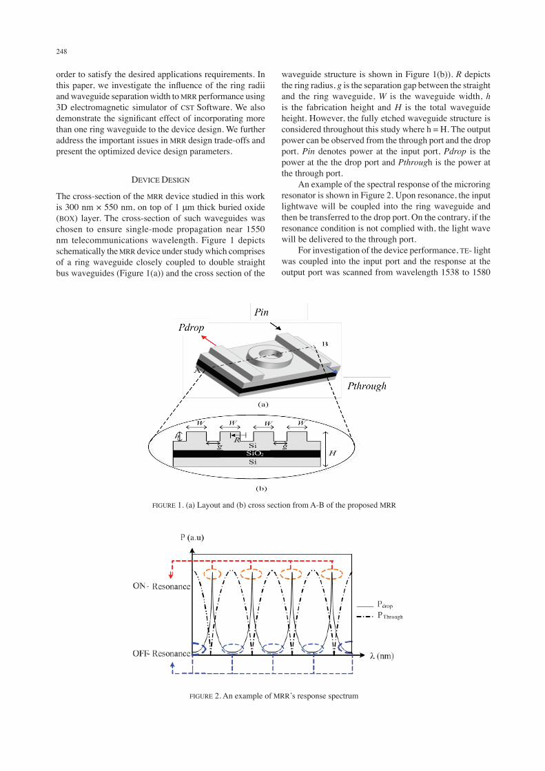
The cross-section of the MRR device studied in this work is 300 nm × 550 nm, on top of 1 μm thick buried oxide (BOX) layer. The cross-section of such waveguides was chosen to ensure single-mode propagation near 1550 nm telecommunications wavelength. Figure 1 depicts schematically the MRR device under study which comprises of a ring waveguide closely coupled to double straight bus waveguides (Figure 1(a)) and the cross section of the
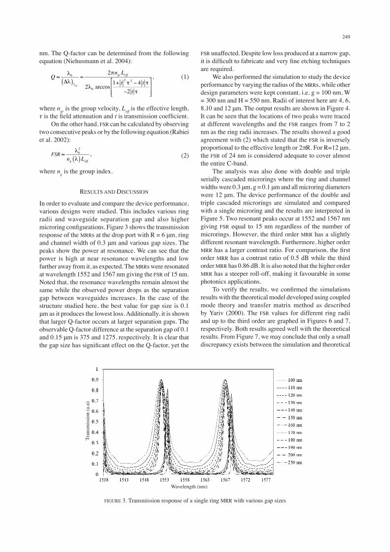
waveguide structure is shown in Figure 1(b)). R depicts the ring radius, g is the separation gap between the straight and the ring waveguide, W is the waveguide width, h is the fabrication height and H is the total waveguide height. However, the fully etched waveguide structure is considered throughout this study where h = H. The output power can be observed from the through port and the drop port. Pin denotes power at the input port, Pdrop is the power at the the drop port and Pthrough is the power at the through port. An example of the spectral response of the microring resonator is shown in Figure 2. Upon resonance, the input lightwave will be coupled into the ring waveguide and then be transferred to the drop port. On the contrary, if the resonance condition is not complied with, the light wave will be delivered to the through port. For investigation of the device performance, TE- light was coupled into the input port and the response at the output port was scanned from wavelength 1538 to 1580
FIGURE 1. (a) Layout and (b) cross section from A-B of the proposed MRR
FIGURE 2. An example of MRR’s response spectrum
249
nm. The Q-factor can be determined from the following equation (Niehusmann et al. 2004):
(1)
where ngr is the group velocity, Leff is the effective length, τ is the field attenuation and t is transmission coefficient. On the other hand, FSR can be calculated by observing two consecutive peaks or by the following equation (Rabiei et al. 2002):
(2)
where ng is the group index.
RESULTS AND DISCUSSION
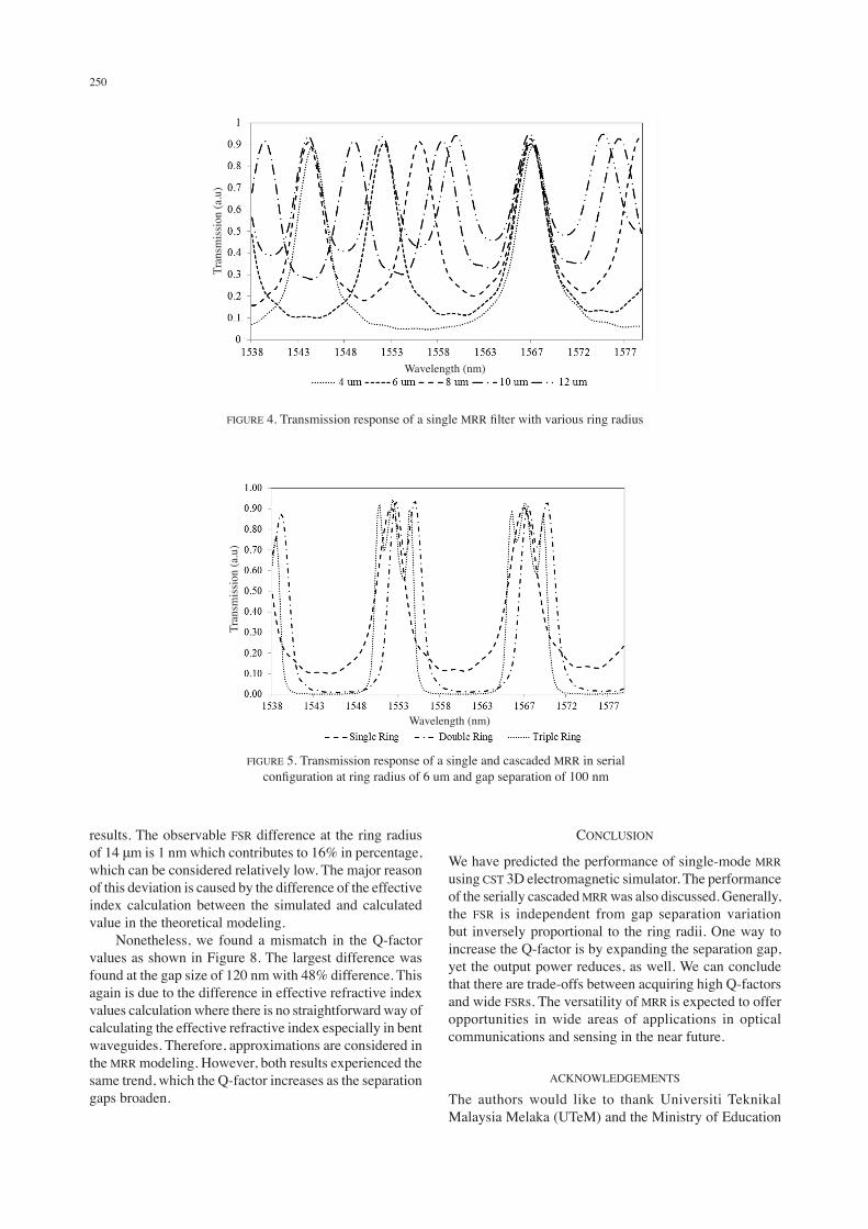
In order to evaluate and compare the device performance, various designs were studied. This includes various ring radii and waveguide separation gap and also higher microring configurations. Figure 3 shows the transmission response of the MRRs at the drop port with R = 6 μm, ring and channel width of 0.3 μm and various gap sizes. The peaks show the power at resonance. We can see that the power is high at near resonance wavelengths and low further away from it, as expected. The MRRs were resonated at wavelength 1552 and 1567 nm giving the FSR of 15 nm. Noted that, the resonance wavelengths remain almost the same while the observed power drops as the separation gap between waveguides increases. In the case of the structure studied here, the best value for gap size is 0.1 μm as it produces the lowest loss. Additionally, it is shown that larger Q-factor occurs at larger separation gaps. The observable Q-factor difference at the separation gap of 0.1 and 0.15 μm is 375 and 1275, respectively. It is clear that the gap size has significant effect on the Q-factor, yet the
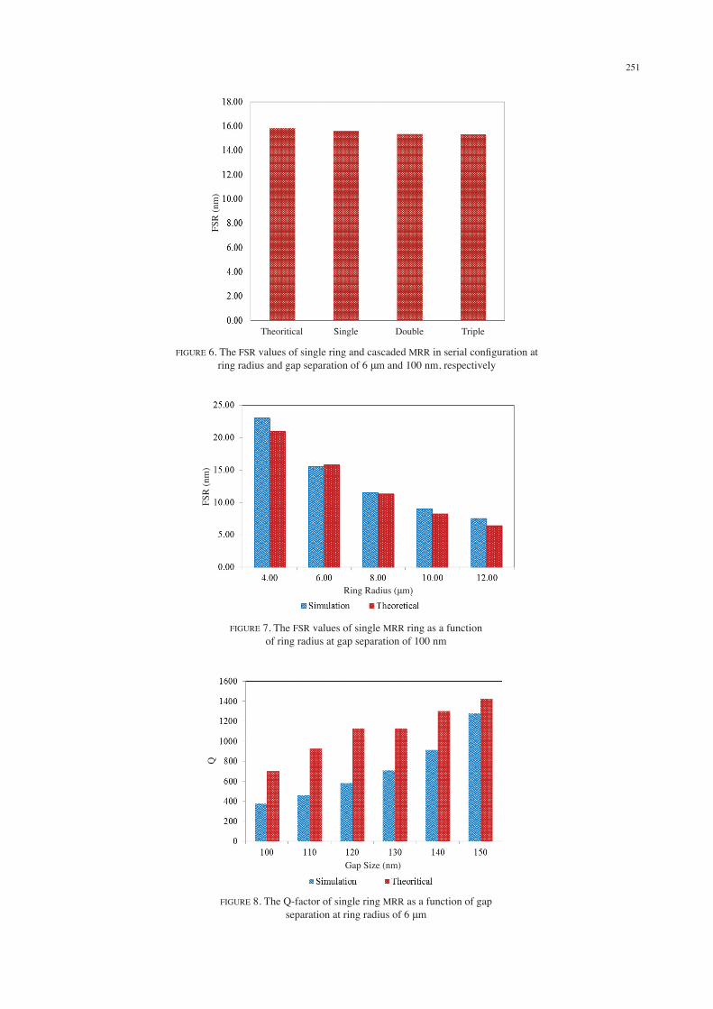
FSR unaffected. Despite low loss produced at a narrow gap, it is difficult to fabricate and very fine etching techniques are required. We also performed the simulation to study the device performance by varying the radius of the MRRs, while other design parameters were kept constant, i.e. g = 100 nm, W = 300 nm and H = 550 nm. Radii of interest here are 4, 6, 8,10 and 12 μm. The output results are shown in Figure 4. It can be seen that the locations of two peaks were traced at different wavelengths and the FSR ranges from 7 to 2 nm as the ring radii increases. The results showed a good agreement with (2) which stated that the FSR is inversely proportional to the effective length or 2πR. For R=12 μm, the FSR of 24 nm is considered adequate to cover almost the entire C-band. The analysis was also done with double and triple serially cascaded microrings where the ring and channel widths were 0.3 μm, g = 0.1 μm and all microring diameters were 12 μm. The device performance of the double and triple cascaded microrings are simulated and compared with a single microring and the results are interpreted in Figure 5. Two resonant peaks occur at 1552 and 1567 nm giving FSR equal to 15 nm regardless of the number of microrings. However, the third order MRR has a slightly different resonant wavelength. Furthermore, higher order MRR has a larger contrast ratio. For comparison, the first order MRR has a contrast ratio of 0.5 dB while the third order MRR has 0.86 dB. It is also noted that the higher order MRR has a steeper roll-off, making it favourable in some photonics applications. To verify the results, we confirmed the simulations results with the theoretical model developed using coupled mode theory and transfer matrix method as described by Yariv (2000). The FSR values for different ring radii and up to the third order are graphed in Figures 6 and 7, respectively. Both results agreed well with the theoretical results. From Figure 7, we may conclude that only a small discrepancy exists between the simulation and theoretical
FIGURE 3. Transmission response of a single ring MRR with various gap sizes
Wavelength (nm)
Tran
smis
sion
(a.u
)
250
results. The observable FSR difference at the ring radius of 14 μm is 1 nm which contributes to 16% in percentage, which can be considered relatively low. The major reason of this deviation is caused by the difference of the effective index calculation between the simulated and calculated value in the theoretical modeling. Nonetheless, we found a mismatch in the Q-factor values as shown in Figure 8. The largest difference was found at the gap size of 120 nm with 48% difference. This again is due to the difference in effective refractive index values calculation where there is no straightforward way of calculating the effective refractive index especially in bent waveguides. Therefore, approximations are considered in the MRR modeling. However, both results experienced the same trend, which the Q-factor increases as the separation gaps broaden.
CONCLUSION
We have predicted the performance of single-mode MRR using CST 3D electromagnetic simulator. The performance of the serially cascaded MRR was also discussed. Generally, the FSR is independent from gap separation variation but inversely proportional to the ring radii. One way to increase the Q-factor is by expanding the separation gap, yet the output power reduces, as well. We can conclude that there are trade-offs between acquiring high Q-factors and wide FSRs. The versatility of MRR is expected to offer opportunities in wide areas of applications in optical communications and sensing in the near future.
ACKNOWLEDGEMENTS
The authors would like to thank Universiti Teknikal Malaysia Melaka (UTeM) and the Ministry of Education
FIGURE 4. Transmission response of a single MRR filter with various ring radius
Wavelength (nm)
Tran
smis
sion
(a.u
)
FIGURE 5. Transmission response of a single and cascaded MRR in serial configuration at ring radius of 6 um and gap separation of 100 nm
Wavelength (nm)
Tran
smis
sion
(a.u
)
251
FIGURE 6. The FSR values of single ring and cascaded MRR in serial configuration at ring radius and gap separation of 6 μm and 100 nm, respectively
Theoritical Single Double Triple
FSR
(nm
)
FIGURE 7. The FSR values of single MRR ring as a function of ring radius at gap separation of 100 nm
Ring Radius (μm)
FSR
(nm
)
FIGURE 8. The Q-factor of single ring MRR as a function of gap separation at ring radius of 6 μm
Gap Size (nm)
Q
252
(MOE), Malaysia for the support. This research is supported by funding from Universiti Kebangsaan Malaysia, Industri-2011-015 and GUP-2012-012. UPI and LIPI are also acknowledged for their contribution via grant no 529/H40.8/TU/2012.
REFERENCES
Belarouci, A., Hill, K.B., Liu, Y., Xiong, Y., Chang, T. & Craig, A.E. 2001. Design and modeling of waveguide-coupled microring resonator. J. Lumin. 94: 35.
Chao, C.Y. & Guo, L.J. 2006. Design and optimization of microring resonators in biochemical sensing applications. IEEE J.of Lightwave Technol. 24: 1395.
Chao, C.Y., Fung, W. & Guo, L.J. 2010. Polymer microring resonators for biochemical sensing applications. Optics Express 18: 393.
Hazura, H., Hanim, A.R., Mardiana, B. & Menon, P.S. 2010. An analysis of silicon waveguide phase modulation efficiency based on carrier depletion effect. International Conference on Semiconductor Electronics Proceedings (ICSE2010), Melaka.
Hazura, H., Mardiana, B., Hanim, A.R., Shaari, S., Menon, P.S., Arsad, N., Mukhtar, W.M. & Abdullah, H. 2012. Design and characterization of multiple coupled microring based wavelength demultiplexer in silicon–on–insulator (SOI). Journal of Nonlinear Optical Physics and Materials 21(1): 1250004(1)-125004(8).
Hryniewicz, J.V., Absil, P.P., Little, B.E., Wilson, R.A. & Ho, P.T. 2000. Higher order filter response in coupled microring resonators. IEEE Photonics Technol. Lett. 12: 320.
Niehusmann, J., Vorckel, A., Haring, B.P., Wahlbrink, T., Henschel, W. & Kurz, H. 2004. Ultra-high quality factor silicon-on-insulator microring resonator. Opt. Lett. 29: 2861.
Rabiei, P., Steier, W.H., Cheng, Z. & Dalton, L.R. 2002. Polymer micro-ring filters and modulators. J. Lightwave Technol. 20: 1968.
Shaari, S., Hanim, A.R., Mardiana, B., Hazura, H. & Menon, P.S. 2010. Modeling and analysis of lateral doping region translation variation on optical modulator performance. AIP Conference Proceedings 1325: 297-300.
Yariv, A. 2000. Universal relations for coupling of optical power between microresonators and dielectric waveguides. Electronic Letters 36(4): 321-322.
Budi Mulyanti & T. HariyadiDepartment of Electrical Engineering EducationIndonesia University of Education (UPI)Jalan Dr. Setiabudhi 207, Bandung 40154Indonesia
P. Susthitha Menon*, Sahbudin Shaari, Hazura Haroon, Abang Annuar Ehsan & B.Y. MajlisInstitute of Microengineering and Nanoelectronics (IMEN)Universiti Kebangsaan Malaysia (UKM)43600 UKM Bangi, SelangorMalaysia
L. Hasanah Department of Physics EducationFaculty of Mathematics and Natural Sciences EducationIndonesia University of Education (UPI) Jalan Dr. Setiabudhi 207, Bandung 40154 Indonesia
D. Mahmudin & G. Wiranto Research Centre for Electronics and TelecommunicationIndonesian Institute of Sciences (LIPI) Jl. Sangkuriang Bandung 40135 Indonesia