1Department of Electronics and Communication Engineering, CGC-CEC Landran, Punjab, India2Punjab Technical University, Punjab, India3Department of Mechanical Engineering, Madanapalle Institute of Technology & Science, AP, India4Arba Minch University, Ethiopia
Correspondence should be addressed to Mohammed Abdella Kemal; [email protected]
Received 13 May 2021; Revised 13 June 2021; Accepted 29 June 2021; Published 13 July 2021
In this paper, RF MEMS switch with capacitive contact is designed and analyzed for Ka band application. A fixed-fixedbeam/meander configuration has been used to design the switch for frequency band 10GHz to 40GHz. Electromagnetic andelectromechanical analysis of three-dimensional (3D) structure/design has been analyzed in multiple finite element method(FEM) based full-wave simulator (Coventorware and high-frequency structure simulator). A comparative study has also beencarried out in this work. The high resistivity silicon substrate (tan δ = 0:010, ρ > 8 kΩ − cm, εr = 11:8) with a thickness of675 ± 25 μm has been taken for switch realization. The designed structure shows an actuation voltage of around 9.2V.Impedance matching for the switch structure is well below 20 dB, loss in upstate, i.e., insertion loss >0.5 dB, and isolationof >25 dB throughout the frequency band is observed for the aforesaid structure. Furthermore, to increase the RFparameters, AIN dielectric material has been used instead of SiO2 resulting in capacitance in downstate that increases henceimproved the isolation. The proposed switch can be utilized in various potential applications such as any switching/tunablenetworks phased-array radar, reconfigurable antenna, RF phase shifter, mixer, biomedical, filter, and any transmitter/receiver(T/R) modules.
1. Introduction
The Micro-Electro-Mechanical-System (MEMS) is anagglomeration of submicron mechanical moving parts andelectronics components/elements on a single module/chip[1]. In the last 20 years, MEMS has spread into the RF regimealso. RF MEMS switches are building blocks for this technol-ogy, without the existence of these switches; RFMEMS seemsto be unimaginable [1, 2]. Nowadays, RF MEMS capacitiveshunt switch has a major role for designing in an advancedcommunication application. RF MEMS switches are prefera-ble to design filters, reconfigurable microwave antenna, andspace communication than solid-state switch like field-effect transistor (FET) and PIN diode. RF MEMS switchesbased on MEMS technology offer many advantageous over
solid-state switches, for example, high isolation, low insertionloss, zero DC power consumption, low noise, more linearity,and used up to millimeter wave [2–4]. MEMS technology-based RF switches have the advantages of miniaturization,monolithically integrated with other IC using batch process-ing technology as compared to other conventional switches.The performance of the RF MEMS shunt switch dependsupon the material used for the membrane and also dependsupon return loss, pull-in voltage, insertion loss, isolation,and switching time [1]. Metal-metal contact in the switchcreates the stiction problem in the switch. Based on MEMStechnology, RF MEMS switches have two types such as shuntswitch and series switch [3]. These series and shunt configu-ration further classified as a capacitive switch and resistiveswitch base upon contact [2]. Series switches are used for a
HindawiWireless Communications and Mobile ComputingVolume 2021, Article ID 2021513, 8 pageshttps://doi.org/10.1155/2021/2021513
low-frequency application due to poor isolation, while for ahigher frequency of application, capacitive switches are used.In capacitive type contact MEMS switch, a dielectric layer isused between the top beam and bottom electrodes for iso-lation. The structure of the membrane can be bridge typeor cantilever type or dip harm type [3–6]. The actuationvoltage of the switch structure can be minimized withbridge structure supporting meanders and step type [1–4].MEMS-based switches are superior in terms of their RFperformances over conventional electromagnetic relays andsolid-state switches [5–8]. As per the configuration, theswitch can be broadly classified into two categories, i.e., seriesand shunt [1, 2]. Generally, series switch utilizes metal-metalcontact, while shunt switches are mostly capacitive in nature[9]. Some sort of actuation force is needed to make theseswitches work. Although several actuation mechanisms arethere, the electrostatic actuation technique is extensively useddue to its negligible DC power consumption, short switchingtime, and compatibility with IC technology [1, 2, 10]. Thereliability of space systems is of utmost importance for theirsmooth operation over a period of 10-15 years of satellite life.A single point failure may cause catastrophe for the wholemission. So, each and every component, be in launch vehi-cle or communication systems need to be highly reliable[8, 11, 12]. Metal contact reliability in series switches hasalways been a concern during long-term reliability tests[13]. A switch based on metal-metal contact normally suffersfrom various issues like electromigration, stiction, metalcreep, dielectric charging, and fatigue over a period of time[12, 14]. Stiction issue in MEMS switch occurs, when surfaceadhesive forces are larger than the restoring force of the beamstructure [15]. Electromigration is a high current densityphenomenon which causes voids in metal lines. While creepdescribes the trends of a material to deform or to move per-manently to relieve stresses, resulting in a long-term revela-tion to levels of stresses due to material deformation, whichare below the yield or final strength of the material [8, 14].Keeping in mind all the abovementioned issues associatedwith metal contact switches, capacitive contact switch wastaken into consideration [8]. A MEMS capacitive shuntswitch serves as a two-state digital capacitor: a smaller capac-itance (fF) is obtained while the switch is in up position,while a larger capacitance value of capacitor (pF) results indownstate of the switch [1, 2]. Generally, RF MEMS capaci-tive switch uses silicon nitride as dielectric layer due to itsmedium dielectric constant (εr = 7:5), which provides theisolation between both electrodes [16]. Other dielectric mate-rial such as TiO2 (εr = 32), strontium titanate oxide (εr = 120[16]), hafnium dioxide (HfO2, εr = 25 [17]), piezoelectric leadzirconate titanate (PZT, εr = 190 [18]), and aluminiumnitride (AIN, εr = 9:8 [19]) can also be utilized because ofhigh dielectric constant in place of silicon nitride layer forimpressive RF performance.
Many researchers and industries around the globe havereported various RF MEMS switches using different mate-rials with various technologies and by varying the electrome-chanical and RF parameters. Somayye et al. developed theshunt switch with reduced air gap using step structure, andAIN dielectric layer is used instead of SiO2 and Si3N4 for
improved isolation, i.e., -58 dB. Chan et al. have developedthe DC contact switch using GaAs substrate at NationalTaiwan University as shown in Figure 1. In this switch,the coplanar waveguide (CPW) line and center conductorare fabricated using gold material and SiO2 was used asa dielectric layer. The authors reported the return loss>20 dB, isolation of >20 dB, and actuation voltage around26-30V [15–23].
Furthermore, Guo et al. [24] developed the low actuationvoltage MEMS switch by utilizing aluminum alloys for mov-able beam. The designed switch shows the low pull-in voltageof 5V for alloy instead of gold material, i.e., 45V. Rao et al.fabricate the MEMS switch using the clamped-clampedstructure of gold beam having thickness 500A0, and thedielectric layer of AIN is deposited by plasma-enhancedchemical vapor deposition (PECVD) process. The authorsreported the actuation voltage of 5.5V and behaviors ofdielectric charging to characterize by the capacitance–voltage(CV) curve method. Goel et al. developed the MEMS seriesswitch having low actuation voltage, improved RF perfor-mance for reconfigurable antenna, and sufficient switchingspeed. The authors reported the pull-in voltage of 5V withreturn loss >20dB and insertion loss >0.4 dB from DC to60GHz. Further, the capacitive shunt switch was fabricatedon a four-mask silicon wafer by utilizing surface microma-chining process technology to report the low actuation volt-age. The PECVD is used to deposit a thin AIN dielectriclayer to improve isolation in the downstate due to a highdielectric constant. Therefore, Thelluir et al. developed thelow pull-in voltage MEMS switch using gold as a beam mate-rial with improved RF performance. Chu et al. fabricate theMEMS switch on GaAs substrate using a pull-in electrodeand inline cantilever beam to achieve “On” and “Off” statesas shown in Figure 2. In this train, spaced holes are etchedinto cantilever beam to achieve the lower pull-in voltage.The measured insertion loss of >3 dB and isolation of>20 dB in the frequency range 1-40GHz was reported.
2. RF Actuation Mechanism
Mechanical actuation and electrical actuation are two parts ofthe RF MEMS switch. Mechanical movement can be realized
Contactarea
CPWStraight
beamsection
Curvedbeam
sectionCrA1
Anchor/upperelectrode
Bottomelectrode
GroundGround Signal
line
Figure 1: Fabricate capacitive shunt switch National TaiwanUniversity [1].
2 Wireless Communications and Mobile Computing
by piezoelectric, electromagnetic, electrostatic, and thermalmechanisms. The common approach used now days iselectrostatic actuation mechanism, due to its advantages likelow DC power consumption, low switching speed, thin layersof material, wide range of contact forces of 50–200μN, andmost importantly tiny electrode size. Its ON-OFF capaci-tance ratio is also very high, but a higher actuation voltageis required. In comparison to electromagnetic actuation,voltage requirement is low but current consumption is high.Coil and ferromagnetic armature are used as an electromag-netic actuator in electromagnetic actuation. In this type ofmechanism, semihard magnetic materials or permanentmagnets allow the addition of a self-latching mechanism.The example of MEMS device that uses this mechanism is amicromechanical relay. A thermal actuator can also be usedto simplify the relay. Thermal actuators include the armatureof a soft magnetic material, permanent magnets, and thermo-sensitive magnetic materials stators. The piezoelectric mech-anism depends upon the piezoelectric effect, and it providesexceptional material characteristics, where elastic deforma-tion is generated by electrical field stimulation. To actuateON or OFF conditions, a downward force is created byattaching a designed piezoelectric actuator to switch themembrane. Reduced pull-in voltage may be obtained byenabling the switch to have a high force by using this mech-anism. This high force permits the air gap height to beincreased with no reduction in another parameter of the
switch such as critical stress and switching speed. Theswitch can also be actuated by using a thermal actuationmechanism. This actuation mechanism includes the ther-mal microactuators. For example, two thick metal postsare linked with the two thermal actuators which act asthe centerline of the CPW transmission line, and theMEMS switch may be trigger ON and OFF by utilizingcurrent or voltage pulses. A very few researchers had beendeveloped the MMES switch using thermal actuation witha huge contact force and large beam spring constant toachieve the low contact resistance and hence enhance thepower handling capacity. Table 1 shows the comparisonsbetween four actuation technologies, which are used toactuate the RF MEMS switch.
3. Design and Working Principal
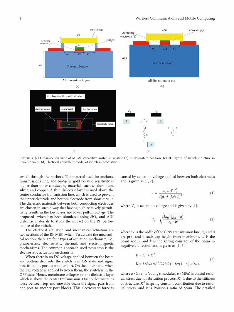
A high resistive silicon wafer (thickness of 675 ± 20 μm,dielectric constant and 11.8) has been used for the develop-ment of MEMS switch using fixed-fixed beam configuration.Figures 3(a) and 3(b) show the cross-section view of the pro-posed MEMS capacitive switch in upstate position anddownstate position, respectively. The coplanar waveguidetransmission line with dimension (G/W/G) of 90/120/90(all in μm) is designed to support the RF MEMS switchwhose characteristics impedance is 50Ω. The grounds ofthe CPW line are connected to both ends of the MEMS
Table 1: Different actuation techniques for MEMS switch.
Technology Contact force (μN) Current (mA) Size Voltage (V) Switching time (μs) Power (mW)
Magnetostatic 50-200 20-150 Medium 3-5 400-1000 0-100
Thermal 500-3500 5-100 Large 3-5 200-10,000 0-200
Piezoelectric 50-250 0 Medium 3-20 50-500 0
Electrostatic 50-1500 0 Small 20-80 1-200 0
Figure 2: Scanning electron microscope image of DC contact switch developed by Chu et al. [17].
3Wireless Communications and Mobile Computing
switch through the anchors. The material used for anchors,transmissions line, and bridge is gold because resistivity ishigher than other conducting materials such as aluminum,silver, and copper. A thin dielectric layer is used above thecenter conductor transmission line, which is used to preventthe upper electrode and bottom electrode from short-circuit.The dielectric materials between both conducting electrodesare chosen in such a way that having high relatively permit-tivity results in the low losses and lower pull-in voltage. Theproposed switch has been simulated using SiO2 and AINdielectric materials to study the impact on the RF perfor-mance of the switch.
The electrical actuation and mechanical actuation aretwo sections of the RF MES switch. To actuate the mechani-cal section, there are four types of actuation mechanism, i.e.,piezoelectric, electrostatic, thermal, and electromagneticmechanisms. The common approach used nowadays is theelectrostatic actuation mechanism.
When there is no DC voltage applied between the beamand bottom electrode, the switch is in ON state and signalpass from one port to another port. On the other hand, whenthe DC voltage is applied between them, the switch is in theOFF state. Hence, membrane collapses on the dielectric layerwhich is above the center transmission. Due to electrostaticsforce between top and movable beam the signal pass fromone port to another port blocks. This electrostatic force is
caused by actuation voltage applied between both electrodesand is given as [1, 2].
F = ε0wWV2a
2 g0 + td/εrð Þ½ �2 , ð1Þ
where Va is actuation voltage and is given by [1].
Va =ffiffiffiffiffiffiffiffiffiffiffiffiffiffiffiffiffiffiffiffiffiffiffiffiffi2kg2 g0 − gð Þ
ε0wW
s, ð2Þ
whereW is the width of the CPW transmission line, g0 and gare pre- and postair gap height from membrane, w is thebeam width, and k is the spring constant of the beam innegative z direction and is given as [1, 5]
where E (GPa) is Young’s modulus, σ (MPa) is biaxial resid-ual stress due to fabrication process, K ′ is due to the stiffnessof structure, K″ is spring constant contribution due to resid-ual stress, and v is Poisson’s ratio of beam. The detailed
Actuatingelectrode (1)
1
675
400
2.5
MEMS bridge
SiO2 (0.1)
12090 90
Silicon substrate
All dimensions in 𝜇m
(a)
Actuatingelectrode (1)
675
400
12090 90
Silicon substrate
All dimensions in 𝜇m
Zero air gap
(b)
2-D layout of the switch structure
Anchor mask Anchor maskBeam mask
Substrate mask
(c)
1 3C
L
Rs
2
1 3
2
Z0 Z0
(d)
Figure 3: (a) Cross-section view of MEMS capacitive switch in upstate (b) in downstate position. (c) 2D layout of switch structure inCoventorware. (d) Electrical equivalent model of switch in downstate.
4 Wireless Communications and Mobile Computing
dimension and material used for the switch structure aregiven in Table 2.
Above a definite threshold voltage, the electrostatic forceis increased due to an increase in charge and overcome themechanical restoring force of the beam. An increase in elec-trostatic force results in a decrease in the beam gap heightand at the same time which in turn enhances the downstatecapacitance, and resulting beam becomes unstable and thisthreshold voltage is called pull-in voltage given as [1, 14]
The electrical equivalent model describes a shunt switch asCLR (capacitance, inductance, resistance) series resonant cir-cuit as shown in Figure 3(d). The movable metallic beam ofthe MEMS shunt switch is sketched by switch variable capac-itance, lumped resistance, and switch inductance. Dependingupon the ON and OFF conditions of the switch, the variablecapacitance is changed. When the switch in ON condition,the variable capacitance is represented by Cup and in OFFcondition it is represent by Cdown. From Eq. (6), if the fre-quency of operation is less than LC resonance frequency,the CLR model works as a capacitor, while it works as aninductor above LC resonant frequency. At the series LCresonant frequency, the CLR (capacitance, inductance, resis-tance) model reduces as series resistance and is representedby Rs. Capacitances in up- and downstate define the insertionand isolation of shunt switch, respectively. The followingsubsections explain these points elaborately. The impedanceof the capacitive shunt switch is given as [5]
Zs = Rs + jωL + 1jωC
, ð5Þ
Zs =
1jωC
for
Rs forjωL for
f<<f0f = f0
f>>f0
8>>><>>>:
9>>>=>>>;, ð6Þ
where C is the capacitance of the switch it may be up capac-itance (Cu) and down capacitance (Cd) depends upon theswitch position, Rs is the bridge resistance and it dependsupon the resistivity of bridge, and L is the bridge inductanceand it depends upon the gap between signal line ground ofCPW. The LC series resonant frequency of the capacitiveshunt MEMS switch is given as [1]
5.1. Pull-In Analysis. The modal analysis and pull-in voltagefor fixed-fixed beam has been carried using the finite element
method- (FEM-) based Coventorware software. At the pull-in voltage, the movable bridge/membrane suddenly collapseson the thin dielectric layer due to the mechanical action ofelectrostatic force and causing the system to unstable(Figure 4). The electromechanical analyses in Coventorwareare shown in Figure 5. It can be seen from the plot as voltageincreases on the center conductor the top movable metallicbeam starts to snap down from the top in the negativez direction towards the dielectric layer due to electrostaticforce. When the metallic beam travel 1/3rd gap of thetotal initial gap from the topside, the movable beam entersinto the instable region/area, and at this condition, electro-static force overcome the restoring force. Small diameters(10 × 10μm2) holes are introduced in the top metal mem-brane to reduce the stiction problem and residual stressduring the release process as shown in Figure 4.
5.2. Switching Time. The switching time depends upon themechanical resonant frequency of the movable beam, appliedsource voltage, and pull-in voltage. It is defined as a timetaken by the movable metallic beam to toggle from actuatedstate to unactuated state and vice versa is called switch speedand is given as [1].
Ts = 3:67Vp
Vsω0, ð8Þ
where Vs is the source voltage and given by Vs = 1:35Vp, ω0is the mechanical resonant frequency and given by as ω0 =ffiffiffiffiffiffiffiffik/m
p, m is the beam mass, and k is the spring constant in
negative z direction. Figure 6 demonstrates the variation ofswitching speed/time with beam thickness to beam length(t/l) ratio. The switching in gold membrane is three timesslower compared to aluminum.
5.3. RF Analysis. The ANSYS HFSS software has been used toextract the RF performance of the designed fixed-fixed beamconfiguration-based MEMS switch. RF parameters such asinsertion loss (S21 in dB) and return loss (S11 in dB) aredefined in upstate, whereas isolation (S21 in dB) is defined
Table 2: Specific parameters of the proposed MEMS switch.
in downstate. When there is no voltage applied to the bottomelectrode, the switch is in unactuated state, and in this state,two RF parameters such as return loss and insertion loss ofthe switch have been analyzed. Return loss state that howmuch power is reflected back by the input/exciting port ofcoplanar waveguide transmission line. This is due to theimproper impedance matching between switch and CPWline. Figure 7 shows the return loss or impedance matchingas a function of frequency is better than 20 dB over wholefrequency band. The return loss (S11) in the up state of theswitch is mathematically calculated by [1]
S11j j2 ≈ ω20C
2upZ
20
4 : ð9Þ
Insertion loss is also calculated in upstate and is it changethe flow of RF signal between the input port and output port
to control the power dissipations in transmission line and isgiven as [1].
S21j j = 11 + jω0CdZ0/2
� �: ð10Þ
Insertion loss happens at low frequency due to the resis-tive loss between contact resistance region of the switch andfinite resistance of CPW line while at high frequency is dueto skin depth. Figure 8 shows the insertion loss better than0.5 dB throughout the frequency band.
Figure 4: 3D view of proposed switch in Coventorware.
0.0
–0.2
–0.4
–0.6
–0.8
–1.00 108642
Voltage (V)
Disp
lace
men
t (𝜇
m)
Pull-in voltage = 9.2 V
Figures 5: Variation of initial gap with applied voltage.
1413121110
9876543
0.0 0.5 1.0 1.5 2.0 2.5 3.0 3.5(t/l)>ratio (𝜇m)
Switc
hing
tim
e (𝜇
s)
GoldAluminum
Figure 6: Variation of switching time (ts) with (t/l) ratio ofRF-MEMS Shunt Switch.
6 Wireless Communications and Mobile Computing
When the proposed shunt MEMS switch is in an actuatedstate, switch capacitance is a large increase in downstate byfactor 20-100 resulting in the good isolation. Isolation defines
as how much power is present between port 1 and port 2when the switch is in OFF state and is given as [2].
S21j j2 = 4ω20Z
20C
2down
, ð11Þ
where Cdown is the downstate capacitance and is given by [1].
Cdown =ε0εrAtd
: ð12Þ
The ratio of capacitance in downstate to upstate isdefined as the figure of merit (FOM). The FOM factor forthe proposed switch is greater than 50. Figure 9 shows theisolation for the proposed switch is better than 20 dB forthe entire frequency band and maximum isolation is 50 dB@18GHz and 55 dB @12GHz for SiO2 and AIN dielectricmaterials, respectively.
In MEMS shunt switch, small diameter holes play thevital role in RF performance as well as in mechanical perfor-mance. Minor diameters holes are inserted into the top mov-able beam to overcome the squeeze air film damping andimprove the switching speed of the switch. The total holesarea may be 65% of the whole structure. Therefore, holesdischarge some of the residual stress in the membrane anddecrease the young modules of the MEMS switch. The effectof holes is negligible in upstate if the holes sizes are less thanthe 3-5 initial air gap because the fringing field can fill thehole area. In downstate, the holes reduced capacitance as wellas isolation of the switch. Figure 10 shows the for holesdimension 5 × 5 μm2 isolation is 65 dB and for 10 × 10μm2
isolation is 60 dB.
6. Conclusion
In this work, a detailed analysis of a designed RF MEMScapacitive type shunt switch is outlined. Fixed-fixed beamconfiguration is chosen here for ease of realization. The
0
–10
–20
–30
–40
–50
–60
–7010 20 30 40
Frequency (GHz)
Isol
atio
n (d
B)
10⁎10 5⁎5
Figure 10: Effect of holes on isolation.
–50
–45
–40
–35
–30
–25
–20
–15
–10
0 10 20 30 40
Frequency (GHz)
S 11 (
dB)
Return loss
Figure 7: Return loss in upstate as a function of frequency.
0.0
–0.1
–0.2
–0.3
–0.4
–0.50 10 20 30 40
Frequency (GHz)
S 21 (
dB)
Insertion loss
Figure 8: Insertion loss in upstate as a function of frequency.
0
–10
–20
–30
–40
–50
–600 10 20 30 40
Frequency (GHz)
AINSiO2
S 21 (
dB)
Figure 9: Isolation in downstate as a function of frequency.
7Wireless Communications and Mobile Computing
operating frequency is targeted for the 10 to 40GHz band.MATLAB is used for all analytical calculation, whereas HFSSand Coventorware are used for the full-wave analysis of theswitch structure. The proposed switch shows the pull-in volt-age around 9.2V for the gold membrane. The RF parameterssuch as isolation, insertion loss, and return loss are >20 dB,>0.5 dB, and >25dB, respectively, over the whole frequencyband for SiO2 as a dielectric layer. Furthermore, to improvethe RF parameters, here, an AIN dielectric material is usedinstead of SiO2 because of the higher dielectric constant toincrease the downstate capacitance and thus improve theisolation. The reported maximum isolation in downstate is55 dB at 15GHz.
Data Availability
Data will be made available on request.
Conflicts of Interest
The authors declare that there is no conflict of interestregarding the publication of this paper.
References
[1] G. G. M. Rebeiz, RF MEMS Theory, Design and Technique,Wiley, Hoboken, 2003.
[2] H. Jaafar, K. S. Beh, N. A. Yunus, W. Z. W. Hasan, S. Shafic,and O. Sidek, “A comprehensive study on RF MEMS switch,”Microsystem Technologies, vol. 20, no. 12, pp. 2109–2121,2014.
[3] K. V. Caekenberghe and K. Sarabandi, “A self-aligned fabrica-tion process for capacitive fixed-fixed beam RFMEMS compo-nents,” Journal of Microelectromechanical Systems, vol. 17,no. 3, pp. 747–754, 2008.
[4] C. Goldsmith, J. Ehmke, A. Malczewski et al., “Lifetime charac-terization of capacitive Rf MEMS switches,” in 2001 IEEEMTT-S International Microwave Sympsoium Digest (Cat.No.01CH37157), pp. 227–230, Phoenix, AZ, USA, May 2001.
[5] C. L. Dai, H. J. Peng, M. C. Liu, C. C. Wu, and L. J. Yang,“Design and fabrication of RF MEMS switch by the CMOSprocess,” Tamkang Journal of Science and Engineering, vol. 8,no. 3, pp. 197–202, 2005.
[6] L. Y. Ma, A. N. Nordin, and N. Soin, “A novel design of a low-voltage low-loss T-match RF-MEMS capacitive switch,”Microsystem Technologies, vol. 24, no. 1, pp. 561–574, 2018.
[7] Y. W. Yu, J. Zhu, S. X. Jia, and Y. Shi, “A high isolation series-shunt RF MEMS switch,” Sensors, vol. 9, no. 6, pp. 4455–4464,2009.
[8] A. Persano, A. Cola, G. de Angelis, A. Taurino, P. Siciliano,and F. Quaranta, “Capacitive RF MEMS switches withtantalum-based materials,” Journal Of MicroelectromechanicalSystems, vol. 20, no. 2, pp. 365–370, 2011.
[9] W. B. Zheng, Q. A. Huang, X. P. Liao, and F. X. Li, “RFMEMSmembrane switches on GaAs substrates for X-band applica-tions,” Journal of Microelectromechanical Systems, vol. 14,no. 3, pp. 464–471, 2005.
[10] H. R. Ansari and S. Khosroabadi, “Design and simulation of anovel RF MEMS shunt capacitive switch with a unique springfor Ka-band application,” Microsystem Technologies, vol. 25,no. 2, pp. 531–540, 2019.
[11] B. Pillans, J. Kleber, C. Goldsmith, and M. Eberly, “RF powerhandling of capacitive RF MEMS devices,” in 2002 IEEEMTT-S International Microwave Symposium Digest (Cat.No.02CH37278), pp. 329–332, Seattle, WA, USA, June 2002.
[12] A. Persano, A. Tazzoli, A. Cola, P. Siciliano, G. Meneghesso,and F. Quaranta, “Reliability enhancement by suitable actua-tion waveforms for capacitive RF MEMS switches in III–Vtechnology,” Journal of Microelectromechanical Systems,vol. 21, no. 2, pp. 414–419, 2012.
[13] Q. Ma, Q. Tran, T. Kuan et al.,Metal Contact Reliability of RFMEMS Switches, Intel Corporation, Santa Clara, CA, USA,2007.
[14] J. Innnaci, “Reliability of MEMS: a perspective on failuremechanisms, improvement solutions and best practices atdevelopment level,” Displays, vol. 37, pp. 62–71, 2015.
[15] N. Kobayashi, A. Takano, and S. Kubono, “Measuringequipment and measurements of adhesion force between goldelectrical contacts,” IEEE Transactions on Components, Pack-aging and Manufacturing Technology-Part A, vol. 21, no. 1,pp. 46–53, 1998.
[16] M. F. B. Badia, E. Buitrago, and A. M. Ionescu, “RF MEMSshunt capacitive switches using AlN compared to Si3N4 dielec-tric,” Journal of Microelectromechanical Systems, vol. 21, no. 5,pp. 1229–1240, 2012.
[17] C. Chu and X. Liao, “One to 40 GHz ultra-wideband RFMEMS direct-contact switch based on GaAs MMIC tech-nique,” IET Microwaves, Antennas & Propagation, vol. 12,no. 6, pp. 879–884, 2017.
[18] A. Ziaei, T. Dean, and Y. Mancuso, “Life time characterizationof capacitive power RF MEMS switch,” in 2005 EuropeanMicrowave Conference, Paris, France, October 2005.
[19] J. Y. Park, G. H. Kim, K. W. Chung, and J. U. Bu, “Monolith-ically integrated micromachined RF MEMS capacitiveswitches,” Sensors and Actuators A: Physical, vol. 89, no. 1-2,pp. 88–94, 2001.
[20] C. L. Goldsmith, Z. Yao, S. Eshelman, and D. Denniston, “Per-formance of low-loss RF MEMS capacitive switches,” IEEEMicrowave and Guided Wave Letters, vol. 8, no. 8, pp. 269–271, 1998.
[21] S. Fouladi and ,R. R. Mansour, “Capacitive RF MEMS switchesfabricated in standard 0.35-μm CMOS technology,” IEEETransactions on Microwave Theory and Techniques, vol. 58,no. 2, pp. 478–486, 2010.
[22] K. Jairath, N. Singh, V. Jagota, andM. Shabaz, “Compact ultra-wide band metamaterial-inspired split ring resonator structureloaded band notched antenna,” Mathematical Problems inEngineering, vol. 2021, Article ID 5174455, 12 pages, 2021.
[23] Z. Deng, H. Wei, S. Fan, and J. Gan, “Design and analysisa novel RF MEMS switched capacitor for low pull-in volt-age application,” Microsystem Technologies, vol. 22, no. 8,pp. 2141–2149, 2016.
[24] F. M. Guo, Z. Q. Zhu, Y. F. Long et al., “Study on low voltageactuated MEMS rf capacitive switches,” Sensors and ActuatorsA: Physical, vol. 108, no. 1–3, pp. 128–133, 2003.