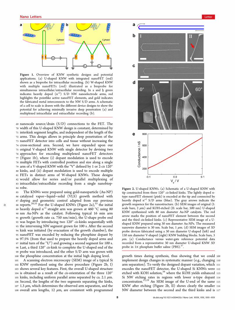
1 Design and Synthesis of Diverse Functional Kinked Nanowire2 Structures for Nanoelectronic Bioprobes3 Lin Xu,†,‡,§ Zhe Jiang,‡,§ Quan Qing,‡,§ Liqiang Mai,† Qingjie Zhang,† and Charles M. Lieber*,†,‡,∥
4†WUT-Harvard Joint Nano Key Laboratory, State Key Laboratory of Advanced Technology for Materials Synthesis and Processing,
5 Wuhan University of Technology, Wuhan 430070, China
6‡Department of Chemistry and Chemical Biology and ∥School of Engineering and Applied Science, Harvard University, Cambridge,
7 Massachusetts 02138, United States
8 *S Supporting Information
9 ABSTRACT: Functional kinked nanowires (KNWs) repre-10 sent a new class of nanowire building blocks, in which11 functional devices, for example, nanoscale field-effect tran-12 sistors (nanoFETs), are encoded in geometrically controlled13 nanowire superstructures during synthesis. The bottom-up14 control of both structure and function of KNWs enables15 construction of spatially isolated point-like nanoelectronic16 probes that are especially useful for monitoring biological17 systems where finely tuned feature size and structure are highly18 desired. Here we present three new types of functional KNWs19 including (1) the zero-degree KNW structures with two parallel heavily doped arms of U-shaped structures with a nanoFET at20 the tip of the “U”, (2) series multiplexed functional KNW integrating multi-nanoFETs along the arm and at the tips of V-shaped21 structures, and (3) parallel multiplexed KNWs integrating nanoFETs at the two tips of W-shaped structures. First, U-shaped22 KNWs were synthesized with separations as small as 650 nm between the parallel arms and used to fabricate three-dimensional23 nanoFET probes at least 3 times smaller than previous V-shaped designs. In addition, multiple nanoFETs were encoded during24 synthesis in one of the arms/tip of V-shaped and distinct arms/tips of W-shaped KNWs. These new multiplexed KNW structures25 were structurally verified by optical and electron microscopy of dopant-selective etched samples and electrically characterized26 using scanning gate microscopy and transport measurements. The facile design and bottom-up synthesis of these diverse27 functional KNWs provides a growing toolbox of building blocks for fabricating highly compact and multiplexed three-28 dimensional nanoprobes for applications in life sciences, including intracellular and deep tissue/cell recordings.
30 The rational design and synthesis of semiconductor31 nanowire (NW) building blocks with controlled structures32 have enabled the bottom-up fabrication paradigm with33 unprecedented flexibility to construct nanoelectronic and34 nanophotonic devices.1−8 The development of NW structures35 from basic one-dimensional (1D)9−11 through two- and three-36 dimensional (2D and 3D)2,12−14 enables novel spatial and37 functional configurations of devices that have proven especially38 advantageous in developing nanoelectronic interfaces with39 biological systems.13−21 In particular, functional KNWs in40 which nanoFETs or field sensitive p-n diodes are synthetically41 integrated in kinked NW superstructures have been used to42 fabricate 3D bend-up nanoelectronic probes to record extra-43 and intracellular action potentials from single cells and44 tissues.14,20 In these nanobiosensors, the development of45 topological and compositional control in silicon NWs has46 enabled the synthesis and fabrication of single-detector probes47 from single 60° or 120° KNWs where the nanoscale detector is48 “presented” away from supporting substrates and bulky metal49 interconnects. However, the synthetic demonstration of more50 (i) complex NW geometries, including multikinked and zigzag-
51shaped NWs14,20,22−31 and (ii) multiple nanoFETs within52single 1D NWs19,32 promise a rich combination of device53designs that could open up distinct sensing applications. To54realize this opportunity requires that several fundamental55questions be addressed, including: (1) Can the probe size be56reduced while at the same time being ca. size-independent away57from the tip so that deep insertions are even less invasive; and58(2) can ab initio design and subsequent synthesis be used to59realize functional multiplexed KNW device arrays with defined60geometry and topology?61Here we address these questions and substantially expand the62scope of functional KNWs building blocks through the ab initio63design and synthesis of several new structures as illustrated64 f1schematically in Figure 1. First, we designed U-shaped KNWs65as compact, high aspect ratio probes (Figure 1a), where three66120° cis-kinks can define the “U”, dopant modulation between67two of these kinks defines nanoFET detector, and heavily68doped (parallel) arms before/after the three kinks function as
69 nanoscale source/drain (S/D) connections to the FET. The70 width of this U-shaped KNW design is constant, determined by71 interkink segment lengths, and independent of the length of the72 arms. This design allows in principle deep penetration of the73 nanoFET detector into cells and tissue without increasing the74 cross-sectional area. Second, we have expanded upon our75 original V-shaped KNW with single detector by devising two76 approaches for encoding multiplexed nanoFET detectors77 (Figure 1b), where (i) dopant modulation is used to encode78 multiple FETs with controlled position and size along a single79 arm of a V-shaped KNW with the “V” defined by 1 or 2-cis 120°80 kinks, and (ii) dopant modulation is used to encode multiple81 FETs in distinct arms of W-shaped KNWs. These designs82 would allow for series and/or parallel multiplexing of83 intracellular/extracellular recording from a single nanobiop-84 robe.85 The KNWs were prepared using gold-nanoparticle (Au-NP)86 catalyzed vapor−liquid−solid (VLS) growth method with87 doping and geometric control adapted from our previous
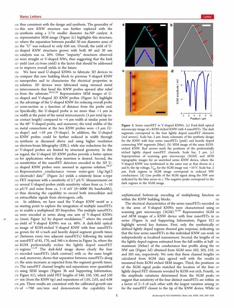
f2 88 reports.20,33 For the U-shaped KNWs (Figure 2a),33 the initial89 heavily doped n+2 straight arm was grown at 460 °C using 8090 nm Au-NPs as the catalyst. Following typical 16 min arm91 growth (growth rate ca. 750 nm/min), the U-shape probe end92 was begun by introducing two 120° cis-kinks sequentially with93 the intervening NW segment grown for 100 s. After the second94 kink was initiated (by evacuation of the growth chamber), the95 nanoFET was encoded by reducing the phosphine dopant by96 97.5% (from that used to prepare the heavily doped arms and97 initial turn of the “U”) and growing a second segment for 100 s.98 Last, a third 120° cis-kink to complete the U-shaped end of the99 probe was introduced, and the other S/D arm was grown with100 the phosphine concentration at the initial high doping level.101 A scanning electron microscopy (SEM) image of a typical Si102 KNW synthesized using the above procedure (Figure 2b, I)103 shows several key features. First, the overall U-shaped structure104 is obtained as a result of the cis-orientation of the three 120°105 kinks, including uniform parallel arms separated by ca. 2.1 μm.106 Second, the lengths of the two segments separating the kinks,107 1.3 μm, which determines the observed arm separation, and the108 overall arm lengths, 12 μm, are consistent with programmed
109growth times during synthesis, thus showing that we could110implement design changes in systematic manner (e.g., changing111arm separation). To verify the designed dopant variation, which112encodes the nanoFET detector, the U-shaped Si KNWs were113etched with KOH solution,34 where the KOH yields enhanced114Si NW etching rates in regions with lower n-type dopant115concentration.11,19 An SEM image of the U-end of the same116KNW after etching (Figure 2b, II) shows clearly the smaller117NW diameter between the second and the third kinks and is
Figure 1. Overview of KNW synthetic designs and potentialapplications. (a) U-shaped KNW with integrated nanoFET (red)shown as a bioprobe for intracellular recording. (b) W-shaped KNWwith multiple nanoFETs (red) illustrated as a bioprobe forsimultaneous intracellular/extracellular recording. In a and b̧ greenindicates heavily doped (n+2) S/D NW nanoelectrode arms, redhighlights the pointlike active nanoFET elements, and gold indicatesthe fabricated metal interconnects to the NW S/D arms. A schematicof a cell to scale is drawn with the different device designs to show thepotential for achieving minimally invasive deep penetration (a) andmultiplexed intracellular and extracellular recording (b).
Figure 2. U-shaped KNWs. (a) Schematic of a U-shaped KNW withtip constructed from three 120° cis-linked kinks. The lightly doped n-type nanoFET element (pink) is encoded at the tip and connected byheavily doped n+2 S/D arms (blue). The gray arrows indicate thegrowth sequence for the nanostructure. (b) SEM images of original (I:scale bare, 2 μm) and KOH-etched (II: scale bar, 500 nm) U-shapedKNW synthesized with 80 nm diameter Au-NP catalysts. The redarrow marks the position of nanoFET element between the secondand the third cis-linked kinks. (c) Representative SEM image of a U-shaped KNW prepared using 30 nm diameter Au-NPs. The measurednanowire diameter is 30 nm. Scale bar, 1 μm. (d) SEM images of 3Dprobe devices fabricated using a 30 nm diameter U-shaped (left) and150 nm diameter V-shaped (right) KNW building blocks. Scale bars, 3μm. (e) Conductance versus water-gate reference potential datarecorded from a representative 30 nm diameter U-shaped KNW 3Dprobe in 1× phosphate buffer saline (PBS).37.
Nano Letters Letter
dx.doi.org/10.1021/nl304435z | Nano Lett. XXXX, XXX, XXX−XXXB
118 thus consistent with the design and synthesis. The generality of119 this new KNW structure was further explored with the120 synthesis using a 2.7× smaller diameter Au-NP catalyst. A121 representative SEM image (Figure 2c) highlights this structure,122 where the separation between parallel 30 nm diameter arms of123 the “U” was reduced to only 650 nm. Overall, the yield of U-124 shaped KNW structures grown with both 80 and 30 nm125 catalysts was ca. 20%. Other “impurity” structures observed126 were straight or V-shaped NWs, thus suggesting that the kink127 yield (not cis/trans yield) is the factor that should be addressed128 to improve overall yields in the future.129 We have used U-shaped KNWs to fabricate 3D devices to130 compare this new building block to previous V-shaped KNW131 nanoprobes and to characterize the electrical properties in132 solution. 3D devices were fabricated using stressed metal133 interconnects that bend the KNW probes upward after relief134 from the substrate.20,35,36 Representative SEM images of U-135 shaped and V-shaped 3D KNW probes (Figure 2c) highlight136 the advantage of the U-shaped KNW for reducing overall probe137 cross-section as a function of distance from the probe end.138 Specifically, the U-shaped probe is no more than ∼1 μm in139 width at the point of the metal interconnects (3 μm total tip-to-140 contact length) compared to ∼4 μm width at similar point for141 the 60° V-shaped probe, and moreover, the total widths of the142 metal connections at the two KNW probes were <3 μm (U-143 shape) and ∼10 μm (V-shape). In addition, the U-shaped144 KNW probes could be further reduced in width through145 synthesis as discussed above and using higher resolution146 electron-beam lithography (EBL), while size reductions for the147 V-shaped probes are limited by structural geometry. In this148 regard, the U-shaped 3D KNW probes provide a better option149 for applications where deep insertion is desired. Second, the150 sensitivities of the nanoFET detectors encoded in the 3D U-151 shaped KNW probes were assessed in aqueous solution.20,37
152 Representative conductance versus water-gate (Ag/AgCl153 electrode) data37 (Figure 2e) yields a relatively linear n-type154 FET response with a sensitivity of 2.7 μS/V. Measurements on155 several U-shaped probes yields sensitivity values from ca. 1−10156 μS/V and noise from ca. 1−4 mV (0−6000 Hz bandwidth),157 thus showing the capability to record both intracellular and158 extracellular signals from electrogenic cells.159 In addition, we have used the V-shape KNW motif as a160 starting point to explore the integration of multiple nanoFETs161 to enable a multiplexed 3D bioprobes. The multiple nanoFETs162 were encoded in series along one arm of V-shaped KNWs
f3 163 (inset, Figure 3a) by dopant modulation,33 where the overall164 yield of V-shaped KNWs was ca. 40%. A dark-field optical165 image of KOH-etched V-shaped KNW with four nanoFETs166 grown for 45 s/each and heavily doped segment growth times167 (between every two adjacent nanoFETs) following the initial168 nanoFET of 85, 170, and 340 s is shown in Figure 3a, where the169 KOH preferentially etches the lightly doped nanoFET170 regions.11,19 The dark-field image shows clearly the four171 encoded nanoFETs (dark contrast) with ca. the same length172 and, moreover, shows that separation between nanoFETs along173 the arms increases as expected from the segment growth times.174 The nanoFET channel lengths and separations were quantified175 using SEM images (Figure 3b and Supporting Information,176 Figure S1), which yield FET lengths of 540, 550, 530, and 530177 nm (from the KNW tip) and separations of 1.05, 2.03, and 4.08178 μm. These results are consistent with the calibrated growth rate179 of ∼700 nm/min and demonstrate the capability for
180sophisticated bottom-up encoding of multiplexing function181within the KNW building blocks.182The electrical characteristics of the series nanoFETs encoded183in the arms of V-shaped KNWs were characterized using184scanning gate microscopy (SGM).32,38 Representative SGM185and AFM images of a KNW device with four nanoFETs in186series (Figure 3c and Supporting Information, Figure S2)187highlight several key features. First, only the synthetically188defined lightly doped regions showed gate response, indicating189that the four series nanoFETs in this individual KNW can work190independently as localized nanosensors. Second, the lengths of191the lightly doped regions estimated from the full widths at half-192maximum (fwhm) of the conductance line profile along the193NW axis (Figure 3d) obtained from SGM were 502, 505, 510,194and 505 nm, respectively. We note that these channel lengths195calculated from SGM data agreed well with the results196measured from KOH etched SEM images. Third, the positions197of the SGM signal peaks matched the location of the four198lightly doped FET elements revealed by KOH wet etch. Fourth,199the amplitude variations determined from the SGM peaks200suggest that sensitivity of the four distinct nanoFETs are within201a factor of 2−3 of each other with the largest variation arising202for the nanoFET closest to the tip of the KNW device. While
Figure 3. Series nanoFET in V-shaped KNWs. (a) Dark-field opticalmicroscopy image of a KOH-etched KNW with 4 nanoFETs. The darksegments correspond to the four lightly doped nanoFET elements(red arrows). Scale bar, 2 μm. Inset, schematic of the synthetic designfor the KNW with four series nanoFETs (pink) and heavily dopedconnecting NW segments (blue). (b) SEM image of the same KOH-etched KNW. Red arrows mark the positions of the preferentiallyetched lightly doped nanoFET channels. Scale bar, 2 μm. (c)Superposition of scanning gate microscopy (SGM) and AFMtopographic images for an unetched series KNW device, where theV-shaped KNW was synthesized in the same way as that shown in aand b; the tip voltage, Vtip, for the SGM image was −10 V. Scale bar, 2μm. Dark regions in SGM image correspond to reduced NWconductance. (d) Line profile of the SGM signal along the NW armindicated by the blue arrow in c. The negative peaks correspond to thedark regions in the SGM image.
Nano Letters Letter
dx.doi.org/10.1021/nl304435z | Nano Lett. XXXX, XXX, XXX−XXXC
203 further synthetic optimization should allow for series devices204 with comparable sensitivities to be prepared, taken together, the205 results demonstrate excellent bottom-up control of doping206 profile, active channel lengths, and positions of nanoFET207 elements in the KNW structures.208 Last, we have extended the topological complexity of the209 original V-shaped KNW by designing and synthesizing W-210 shaped KNWs where one nanoFET detector is encoded at the211 tips of each of the two “Vs” making up the W-shaped structure
f4 212 (inset, Figure 4a). In this manner, independent, parallel
213 multiplexing with a single probe can be implemented (see214 below). The key structural feature needed to realize the W-215 shaped building block is trans-oriented kink at the central bend216 of the “W” relative to the two cis-kinks that define each of the217 V-shaped tip components of the structure. An SEM image of a218 W-shaped nanostructure (Figure 4a) highlights several key219 points. First, all of the bends defining the W-shape are defined220 by 60° angles at defined positions during growth. Second, each221 of the three 60° angles was introduced with two 120° cis-kinks222 with controlled tip widths of ca. 200 nm. Third, the 120° kinks223 separated by the ca. 4.5 μm arms have a trans-orientation as224 required to realize the “W” structure; we note that this is225 consistent with previous studies20 that showed a higher yield of226 trans linkages was realized as the separation between 120° kinks227 was increased. Last, the overall yield of the W-shaped structure228 was ca. 10%, where other “impurity” structures typically had229 few numbers of kinks. This result suggests that as with the U-230 shaped probes overall yield could be improved in the future by231 increasing the yield of kink formation.232 The positions of the nanoFETs encoded in the W-shaped233 were verified using the selective KOH etching described above.234 A representative dark-field optical microscopy image (Figure235 4b) shows clearly that there is one lightly doped nanoFET at236 each probe tip and that the distance between the two nanoFET237 elements is ca. 4.5 μm. The spatial resolution of or separation
238between these parallel-nanoFETs, is determined by the length239of the arms and the angle of the kinks. Currently the highest240resolution is ∼3 μm, although this could be further reduced to241the submicrometer range by incorporating the zero-degree242KNWs element at the central bend of the “W” or increasing to243ca. 10 μm by using a single 120° kink at this central bend.244To evaluate the multiplexing capability of the W-shaped245KNW structures, we fabricated 3D probe devices where a246common source connection was made to the central bend of247the “W” and two independent drain connections were made to248the outer arms of the structure.35 A representative SEM image249of W-shaped KNW probe connected in this manner (Figure2504c) shows that the probe bends upward uniformly from the251substrate and presents both nanoFETs encoded in the two tips252of the inverted “W” at the same height from the substrate.253Water-gate measurements (Figure 4d) showed that the254sensitivities of the two nanoFETs were 3.8 and 5.7 μS/V,255which are comparable to the performance of single-kinked NW256probes.20 These results demonstrate that bottom-up designed257parallel-nanoFETs in a single W-shaped KNW can work as258independent multiplexed 3D nanosensors. We note that the key259features of this unique multiplexed probe were all controlled260during NW synthesis, which provides a potentially higher level261of flexibility and precision compared to the postgrowth262assembly of single-detector KNW devices.263In conclusion, we have designed and synthesized in good264yield three new types of functional KNWs including (1) U-265shaped KNW structures with two parallel heavily doped arms266connecting a nanoFET at the tip of the “U”, (2) series267multiplexed functional KNW integrating multi-nanoFETs along268the arm and at the tips of V-shaped structures, and (3) W-269shaped multiplexed KNWs integrating nanoFETs at the two270tips of W-shaped structures. The U-shaped KNWs were271synthesized with parallel arm separations as small as 650 nm272and were used to fabricate 3D nanoFET probes at least three273times smaller than previous V-shaped designs. Second, four274nanoFETs were encoded in precise positions by synthesis in275one arm/tip of V-shaped building blocks, and SGM measure-276ments demonstrated that the series detectors had similar277sensitivities that have potential for recording both extracellular278and intracellular action potentials. Third, two nanoFETs were279encoded in distinct arms of the new W-shaped KNW, and these280building blocks were used to fabricate 3D nanoprobes capable281of parallel multiplexing measurements using the independently282addressable nanoFET detectors. The facile design and bottom-283up synthesis of these diverse functional KNWs provides a284greatly expanded toolbox of building blocks for fabricating285highly compact and multiplexed three-dimensional nanoprobes286for applications in life sciences, including (1) deep intracellular287and deep tissue recordings with the ultrasmall U-shaped probes,288(2) series multiplexed recording, for example for simultaneous289intracellular and extracellular responses, using the new V-290shaped probes having detectors spatially encoded along a single291arm, and (3) parallel multiplexing, for example for simulta-292neous, independent recording of at least two intracellular293signals from spatially defined positions within a single cell.
294■ ASSOCIATED CONTENT
295*S Supporting Information296Additional information and figures. This material is available297free of charge via the Internet at http://pubs.acs.org.
Figure 4. Parallel nanoFET KNWs. (a) SEM image of a W-shapedparallel-nanoFET KNW. Scale bar, 2 μm. Inset: Schematic of the W-shaped KNW with one nanoFET encoded at the tip of each V-shapedcomponent of the “W”, where blue and pink indicate heavily dopedconnections and lightly doped nanoFET channels, respectively. (b)Dark-field optical microscopy image of KOH etched W-shaped KNW.The two dark color segments correspond to the lightly dopednanoFET elements (red arrows) near the two tips. Scale bar, 2 μm. (c)SEM image of W-shaped parallel-nanoFET KNW bend-up probe.Scale bar, 20 μm. (d) Conductance versus water-gate referencepotential data recorded independently from two parallel nanoFETs.
Nano Letters Letter
dx.doi.org/10.1021/nl304435z | Nano Lett. XXXX, XXX, XXX−XXXD
302 These authors contributed equally to this work.
303 Notes304 The authors declare no competing financial interest.
305 ■ ACKNOWLEDGMENTS
306 Work at Wuhan University of Technology was supported by307 the National Bas ic Research Program of China308 (2013CB934103, 2012CB933003), the National Natural309 Science Foundation of China (51272197, 51072153), Program310 for New Century Excellent Talents in University (NCET-10-311 0661), the International S&T Cooperation (2013ZR02930),312 and the Fundamental Research Funds for the Central313 Universities (2011-YB-01). Research at Harvard was supported314 by NIH Director’s Pioneer (1DP1OD003900) and DOD315 NSSEFF (N00244-09-1-0078) Awards.
316 ■ REFERENCES(1)317 Lieber, C. M. MRS Bull. 2011, 36, 1052−1063.(2)318 Tian, B.; Lieber, C. M. Pure Appl. Chem. 2011, 83, 2153−2169.(3)319 Schmidt, V.; Wittemann, J. V.; Gosele, U. Chem. Rev. 2010, 110,
320 361−388.(4)321 Mai, L.; Yang, F.; Zhao, Y.; Xu, X.; Xu, L.; Hu, B.; Luo, Y.; Liu, H.
322 Mater. Today 2011, 14, 346−353.(5)323 Wang, Z. L. MRS Bull. 2012, 37, 814−827.(6)324 Wu, H.; Cui, Y. Nano Today 2012, 7, 414−429.(7)325 Yang, P. MRS Bull. 2012, 37, 806−813.(8)326 Wacaser, B. A.; Dick, K. A.; Johansson, J.; Borgstrom, M. T.;
327 Deppert, K.; Samuelson, L. Adv. Mater. 2009, 21, 153−165.(9)328 Yan, H.; Choe, H. S.; Nam, S. W.; Hu, Y.; Das, S.; Klemic, J. F.;
329 Ellenbogen, J. C.; Lieber, C. M. Nature 2011, 470, 240−244.(10)330 Tian, B.; Zheng, X.; Kempa, T. J.; Fang, Y.; Yu, N.; Yu, G.;
331 Huang, J.; Lieber, C. M. Nature 2007, 449, 885−890.(11)332 Kempa, T. J.; Tian, B.; Kim, D. R.; Hu, J.; Zheng, X.; Lieber, C.
333 M. Nano Lett. 2008, 8, 3456−3460.(12)334 Jiang, X.; Tian, B.; Xiang, J.; Qian, F.; Zheng, G.; Wang, H.; Mai,
335 L.; Lieber, C. M. Proc. Natl. Acad. Sci. U.S.A. 2011, 108, 12212−12216.(13)336 Duan, X.; Gao, R.; Xie, P.; Cohen-Karni, T.; Qing, Q.; Choe, H.
337 S.; Tian, B.; Jiang, X.; Lieber, C. M. Nat. Nanotechnol. 2012, 7, 174−338 179.
(14)339 Jiang, Z.; Qing, Q.; Xie, P.; Gao, R.; Lieber, C. M. Nano Lett.340 2012, 12, 1711−1716.
(15)341 Zheng, G.; Patolsky, F.; Cui, Y.; Wang, W. U.; Lieber, C. M.342 Nat. Biotechnol. 2005, 23, 1294−1301.
(17)345 Yan, R.; Park, J. H.; Choi, Y.; Heo, C. J.; Yang, S. M.; Lee, L. P.;346 Yang, P. Nat. Nanotechnol. 2012, 7, 191−196.
(18)347 Gao, R.; Strehle, S.; Tian, B.; Cohen-Karni, T.; Xie, P.; Duan, X.;348 Qing, Q.; Lieber, C. M. Nano Lett. 2012, 12, 3329−3333.
(19)349 Cohen-Karni, T.; Casanova, D.; Cahoon, J. F.; Qing, Q.; Bell, D.350 C.; Lieber, C. M. Nano Lett. 2012, 12, 2639−2644.
(20)351 Tian, B.; Cohen-Karni, T.; Qing, Q.; Duan, X.; Xie, P.; Lieber,352 C. M. Science 2010, 329, 830−834.
(21)353 Qing, Q.; Pal, S. K.; Tian, B.; Duan, X.; Timko, B. P.; Cohen-354 Karni, T.; Murthy, V. N.; Lieber, C. M. Proc. Natl. Acad. Sci. U.S.A.355 2010, 107, 1882−1887.
(22)356 Tian, B.; Xie, P.; Kempa, T. J.; Bell, D. C.; Lieber, C. M. Nat.357 Nanotechnol. 2009, 4, 824−829.
(23)358 Musin, I. R.; Filler, M. A. Nano Lett. 2012, 12, 3363−3368.(24)359 Lee, G.; Woo, Y. S.; Yang, J. E.; Lee, D.; Kim, C. J.; Jo, M. H.
360 Angew. Chem., Int. Ed. 2009, 48, 7366−7370.
(25) 361Lugstein, A.; Steinmair, M.; Hyun, Y. J.; Hauer, G.; Pongratz, P.;362Bertagnolli, E. Nano Lett. 2008, 8, 2310−2314.
(26) 363Madras, P.; Dailey, E.; Drucker, J. Nano Lett. 2009, 9, 3826−3643830.
(27) 365Ben-Ishai, M.; PatoLsky, F. Nano Lett. 2012, 12, 1121−1128.(28) 366Geaney, H.; Dickinson, C.; Weng, W.; Kiely, C. J.; Barrett, C.
367A.; Gunning, R. D.; Ryan, K. M. Cryst. Growth Des. 2011, 11, 3266−3683272.
(29) 369Schwarz, K. W.; Tersoff, J. Nano Lett. 2011, 11, 316−320.(30) 370Ross, F. M. Rep. Prog. Phys. 2010, 73, 114501 (21pp).(31) 371Kim, J. H.; Moon, S. R.; Kim, Y.; Chen, Z. G.; Zou, J.; Choi, D.
372Y.; Joyce, H. J.; Gao, Q.; Tan, H. H.; Jagadish, C. Nanotechnology 2012,37323, 115603 (6pp).
(32) 374Yang, C.; Zhong, Z.; Lieber, C. M. Science 2005, 310, 1304−3751307.
(33) 376The three types of functional KNWs described in this paper377were synthesized as follows. (1) The U-shaped KNWs were378synthesized by chemical-vapor deposition (CVD) through a nano-379particle-catalyzed VLS process as described previously.20 Specifically,38030, 80, or 150 nm diameter gold nanoparticles (Ted Pella) were381dispersed on Si growth substrates with 600 nm SiO2 layer (Nova382Electronic Materials). Growth of heavily phosphorous-doped n-type383arm was first carried out by feeding SiH4 (1 sccm, 99.9999%), PH3 (4384sccm, 1000 ppm in H2), and H2 (60 sccm) into the system (atom ratio385of Si:P is 250:1) for 16 min at a total pressure of 40 Torr and386temperature of 460 °C. The growth was then paused for 15 s to387introduce one 120° kink, by rapidly evacuating the chamber to lowest388pressure and shutting off the gas lines. The following two 120° cis-389kinks were introduced via the same procedure, with a 40−100 s390growth time between every two cis-linked kinks. To grow the lightly391doped n-type FET segment between the second and the third 120° cis-392kinks at the tip, the flow rates of SiH4 (99.9999%) and PH3 (1000 ppm393in H2) were 1 and 0.5 sccm (atom ratio of Si:P is 2000:1, for 30 nm394diameter nanowires) or 1 and 0.1 sccm (atom ratio of Si:P is 10,000:1395for 80 and 150 nm diameter nanowires). Finally, the second heavily396doped n-type arm was allowed to finish in additional 16 min. (2)397Series multi-nanoFET KNWs were grown with reactant gas flow rates,398total gas pressure, and growth temperature the same to U-shaped399KNWs described in (1). Initially, the first heavily doped n+2 arm (atom400ratio of Si:P is 250:1) was grown for 30 min, and the reactor was then401evacuated for 15 s to introduce a 120° kink, then the n+2 tip segment402was grown for 20 s followed by evacuating the reactor for 15 s again to403introduce another 120° cis-linked kink. The lightly doped nanoFET404segments (atom ratio of Si:P is 10 000:1) with intentionally varied405distance were grown and encoded in the second n+2 arm, in which the406growth time for each nanoFET element was 45 s, and growth times for407the n+2 segment between two adjacent nanoFETs were 85, 170, and408340 s, respectively. The total growth time of the second arm was 30409min. Dopant modulation was achieved by varying the flow rates of PH3
410(1000 ppm in H2) at 4 and 0.1 sccm for heavily doped n+2- and lightly411doped n-type segments respectively and kept the flow rates of SiH4 (1412sccm, 99.9999%) and H2 (60 sccm) constant. (3) The growth413temperature and reactant gas pressures of parallel-nanoFET multi-414kinked NWs were the same to U-shaped KNWs described in (1).415Specifically, using 150 nm diameter gold catalysts, the four heavily416doped n+2 arms (atom ratio of Si:P is 250:1) were grown for 6−18417min, respectively (Initial arm was grown 10 min longer than other418three arms), and all adjacent arms were connected by a 60° tip419constructed from two cis-linked 120° kinks. Lightly doped nanoFET420elements (atom ratio of Si:P is 10,000:1) with growth time of 45 s421were introduced immediately after each probe tip growth. Dopant422modulation was achieved by varying the flow rates of PH3 (1000 ppm423in H2) at 4 and 0.1 sccm for heavily doped n+2- and lightly doped n-424type segments, respectively, and the flow rates of SiH4 (1 sccm,42599.9999%) and H2 (60 sccm) were kept constant.
(34) 426We used KOH selective wet etching to analyze the doping427profile of the KNWs encoded with nanoFETs. Briefly, 10 g of KOH428(Sigma-Aldrich Inc.) was dissolved in 88 mL of deionized H2O and 37429mL of isopropanol. Substrates with dispersed NWs were dipped in
Nano Letters Letter
dx.doi.org/10.1021/nl304435z | Nano Lett. XXXX, XXX, XXX−XXXE
430 buffered hydrogen fluoride (BHF) solution (Transene Company Inc.)431 for 10 s followed with deionized H2O rinse and then immediately432 dipped in this KOH solution for 3−10 s at 50−60 °C. The substrates433 were rinsed with deionized H2O, followed with isopropanol rinse and434 N2 blow drying.
(35)435 The bend-up probes were fabricated on Si substrates (Nova436 Electronic Materials, n-type 0.005 Ω cm) with 600 nm SiO2 layer. A437 nickel sacrificial layer (100 nm) was first defined by electron beam438 lithography (EBL) and thermal evaporation (TE). The substrate was439 then coated with SU-8 resist (2000.5, MicroChem Corp.), on which440 the as-synthesized KNWs suspended in ethanol were deposited. After441 definition of the bottom SU-8 support layer by EBL, S/D metal442 contacts were defined by EBL and metalized by thermal evaporation of443 Ti/Pd/Ti (1.5/120/60 nm). Typically, the S/D contact separation was444 0.5−1 μm for U-shaped KNW probe and 10−15 μm for V-shaped445 KNW probe, and the free end of the NW extended 3−4 μm from the446 source contact. The top SU-8 layer was subsequently defined by EBL447 for passivation. Etching of the nickel sacrificial layer (∼1 h) in nickel448 etchant (TFB, Transene Company, Inc.) yielded the 3D bend-up449 probes.
(36)450 Tian, B.; Liu, J.; Dvir, T.; Jin, L.; Tsui, J. H.; Qing, Q.; Suo, Z.;451 Langer, R.; Kohane, D. S.; Lieber, C. M. Nat. Mater. 2012, 11, 986−452 994.
(37)453 The water-gate measurements were carried out in 1× phosphate454 buffer saline (PBS). An Ag/AgCl wire was used as a reference455 electrode. The KNW device conductance was measured with dc bias456 set to 0.1 V, and the current was converted to voltage with a current457 preamplifier (model 1211, DL Instruments) at sensitivity of 10−6 A/V,458 before low-pass filtered (0−6 kHz, CyberAmp 380, Molecular459 Devices) and digitized at 20 kHz sampling rate (Axon Digi1440A,460 Molecular Devices).
(38)461 The device chip was mounted on a BioScope MultiMode SPM462 stage (Digital Instrument). The S/D voltage across the device was kept463 constant at 0.1 V, and S/D current was measured using a low-noise464 differential preamplifier (SR560, Stanford Research Systems). The465 device conductance was calculated from S/D voltage and current. A466 conductive AFM tip (PPP-NCHPt, Nanosensors) was used as a local467 gate and scanned over the device to map the conductance image in468 “Lift Mode”. Specifically, first, for each scan line, zero potential was469 applied to the tip, and a topographic image was acquired in Tapping470 Mode with feedback enabled. The tip was then lifted up 30 nm, and a471 tip potential of ±10 V was applied. The tip was scanned across the472 same line again following the captured topological profile with473 feedback turned off, when the change of conductance of the device was474 recorded.
Nano Letters Letter
dx.doi.org/10.1021/nl304435z | Nano Lett. XXXX, XXX, XXX−XXXF