Design and VHDL Implementation of an Application-Specific Instruction Set Processor Lauri Isola School of Electrical Engineering Thesis submitted for examination for the degree of Master of Science in Technology. Espoo 19.12.2019 Supervisor Prof. Jussi Ryynänen Advisor D.Sc. (Tech.) Marko Kosunen
Transcript
Design and VHDL Implementationof an Application-SpecificInstruction Set Processor
Lauri Isola
School of Electrical Engineering
Thesis submitted for examination for the degree of Masterof Science in Technology.Espoo 19.12.2019
Author Lauri IsolaTitle Design and VHDL Implementation of an Application-Specific Instruction Set
ProcessorDegree programme Computer, Communication and Information SciencesMajor Signal, Speech and Language Processing Code of major ELEC3031Supervisor Prof. Jussi RyynänenAdvisor D.Sc. (Tech.) Marko KosunenDate 19.12.2019 Number of pages 66+45 Language EnglishAbstract
Open source processors are becoming more popular. They are a cost-effectiveoption in hardware designs, because using the processor does not require anexpensive license. However, a limited number of open source processors are stillavailable. This is especially true for Application-Specific Instruction Set Processors(ASIPs).
In this work, an ASIP processor was designed and implemented in VHDLhardware description language. The design was based on goals that make theprocessor easily customizable, and to have a low resource consumption in a System-on-Chip (SoC) design. Finally, the processor was implemented on an FPGA circuit,where it was tested with a specially designed VGA graphics controller.
Necessary software tools, such as an assembler were also implemented for theprocessor. The assembler was used to write comprehensive test programs for testingand verifying the functionality of the processor.
This work also examined some future upgrades of the designed processor. Theupgrades include improvements to hardware, software tools and usability. Thesource codes for the processor, graphics controller and test programs are publishedunder the MIT license, and are available at:http://www.iki.fi/lauri.isola/asip38.Keywords ASIP, CPU, RTL, HDL, FPGA, SoC, programmable logic, embedded
Tekijä Lauri IsolaTyön nimi Sovelluskohtaisen käskykantaprosessorin suunnittelu ja toteutus
VHDL:lläKoulutusohjelma Computer, Communication and Information SciencesPääaine Signal, Speech and Language Processing Pääaineen koodi ELEC3031Työn valvoja Prof. Jussi RyynänenTyön ohjaaja TkT Marko KosunenPäivämäärä 19.12.2019 Sivumäärä 66+45 Kieli EnglantiTiivistelmä
Avoimen lähdekoodin prosessorit ovat yleistymässä. Ne ovat laitteistosuunnitte-lun kannalta kustannustehokas vaihtoehto, koska prosessorin käyttäminen ei vaadikallista lisenssiä. Avoimen lähdekoodin prosessoreita on tarjolla kuitenkin vielä var-sin rajallinen määrä. Tämä koskee etenkin sovelluskohtaisia käskykantaprosessoreita(ASIP).
Tässä työssä on suunniteltu sovelluskohtainen käskykantaprosessori ja toteutet-tu se VHDL-laitteistokuvauskielellä. Suunnittelun lähtökohtina olivat prosessorinvaivaton muokattavuus sekä toteuttaminen järjestelmäpiirille (SoC) mahdollisim-man vähillä resursseilla. Prosessori on toteutettu FPGA-piirille, jossa sitä testattiinerikseen suunnitellulla VGA-grafiikkaohjaimella.
Prosessoria varten toteutettiin myös tarvittavat ohjelmistotyökalut, kuten as-sembler-kääntäjä. Sen avulla kirjoitettiin kattavat testiohjelmat, joita käytettiinprosessorin toiminnan testaamiseksi ja todentamiseksi.
Tässä työssä tutustuttiin myös prosessorin jatkokehittämiseen. Tarkastelussaolivat laitteistoon, ohjelmistotyökaluihin ja käytettävyyteen liittyvät kehitysideat.Prosessorin, grafiikkaohjaimen sekä testiohjelmien lähdekoodit on julkaistu MIT-lisenssillä ja ne ovat saatavilla osoitteessa:http://www.iki.fi/lauri.isola/asip38.Avainsanat ASIP, CPU, RTL, HDL, FPGA, SoC, ohjelmoitavat piirit, sulautetut
PrefaceI have done a number of electronics projects using a variety of microcontrollers.Although microcontrollers have generally served their job well, they have sometimeslacked features that would have been useful in those projects. The idea of makingmy own ASIP processor started to seriously interest me when small FPGAs becamemore affordable to be used in enthusiast-level projects. When using an ASIP,the instruction set of the processor, as well as other features, can be specificallydesigned according to the project. This brings the projects to a whole new level.
This thesis is a documentation of the results of my ASIP project. I wouldlike to thank Aalto University especially for Computer Architecture and DigitalMicroelectronics I & II courses, which contained the basic knowledge of the topic.Thanks also to Nokia Networks for the interest in my ASIP processor. Finally, Iwould like to thank my family for supporting me during my studies.
Abbreviations3D Three-dimensionalAC AccumulatorALU Arithmetic Logic UnitASIC Application-Specific Integrated CircuitASIP Application-Specific Instruction Set ProcessorBRAM Block RAMCISC Complex Instruction Set ComputerCPI Cycles Per InstructionCPU Central Processing UnitDSP Digital Signal ProcessingFF Flip-FlopFPGA Field-Programmable Gate ArrayFSM Finite State MachineHDL Hardware Description LanguageHLL High-Level LanguageI/O Input/OutputIC Integrated CircuitIR Instruction RegisterISA Instruction Set ArchitectureISR Interrupt Service RoutineIP Intellectual PropertyLUT Look-up TableNRE Non-Recurring EngineeringPC Program CounterPLD Programmable Logic DeviceRAM Random Access MemoryROM Read-Only MemoryRISC Reduced Instruction Set ComputerRTL Register Transfer LevelRTOS Real-Time Operating SystemSoC System-on-ChipSP Stack PointerTOS Top Of StackuC MicrocontrolleruP MicroprocessorVHDL VHSIC Hardware Description LanguageVHSIC Very High Speed Integrated CircuitVGA Video Graphics ArrayWNS Worst Negative Slack
10
1 IntroductionA soft processor core is usually described with a Hardware Description Language(HDL) which is converted into an optimized gate-level representation using logicsynthesis [1]. The synthesis result can then implement the functionality of theprocessor inside of a Field-Programmable Gate Array (FPGA), or some otherProgrammable Logic Device (PLD) [2].
Recent development has been towards soft processors which are completelyopen source. For example, processor architectures such as RISC-V are getting intolarge-scale production due their open source license [3]. Even a previously closedMIPS architecture has now been released without any license fees or royalties [4].At the same time, the demand of integrated circuits is increasing due to growingmarkets of Internet of Things (IoT) devices. According to data from IoT Analytics,about 8.3 billion internet-connected devices exist in 2019 [5]. In the future, IoTdevices will be everywhere and include every aspect of life. An estimated numberof IoT devices is 41.6 billion by 2025 [6].
The ongoing development presumably increases the demand for different typesof open source processors. With growing IoT market, the focus is towards small,portable and self-powered devices [7, 8]. This brings the challenge of makingcomputations more energy efficient. Instead of using general-purpose processors,a processor can be customized for the specific application to achieve the bestcombination of performance, power and size. This type of processor is called anApplication-Specific Instruction Set Processor (ASIP) [2].
In computing, hardware acceleration is used to perform functions more efficientlythan a software which is run on a general-purpose processor. An ASIP often providesthe much needed flexibility between hardware accelerators and general-purposeprocessors. [2] For example, an ASIP can be used as an alternative for hardwareaccelerators, or it can serve as a main processor for a number of accelerators [9, 10].
The list of open source ASIPs is still relatively short. Open source websitessuch as OpenCores [11] or GitHub [12] do not seem to have a processor core withthe characteristics of a small and easily customizable ASIP. However, this type ofprocessor could be useful for providing some flexibility for the system designers.
1.1 Thesis goalsThe aim of this thesis is to study the core knowledge and skills required to implementan ASIP processor. Furthermore, the goal is to design and implement an opensource ASIP which is small and easily customizable. To consider the processorsuccessful, its whole datapath and instruction set must be easily modifiable. Inthis way, the processor can be customized for many different applications.
Due to programmability, the primary target device for the ASIP is an FPGA, but
other platforms are also considered during the design process. To make the processorcompatible with FPGAs, the processor’s instruction cycle must support differentmemory configurations inside of an FPGA. This is an important requirement asthe processor cannot be tied to a single type of memory.
The implementation size of the processor should be minimized in order to savelogic resources, and to reduce the complexity and the power consumption of thedesign. The processor architecture must be also optimized for achieving the bestpossible performance. Finally, necessary tools for software development need to beimplemented. Below is a summary of general design goals which need to be met.
• Customizable. The structure of the processor needs to be easily modifiable.
• Compatible. Processor must support different memory configurations insideof an FPGA.
• Small implementation size. Resource usage must be low.
• High performance. Optimizing the processor for performance.
• Usable. Necessary software development tools must be implemented.
For testing the ASIP in an FPGA, a complete prototype of an ASIP controlledsystem is implemented. Therefore, some extra hardware needs to be implemented fortesting purposes. A VGA graphics controller is a good choice for testing hardware,as it displays the outputs of the ASIP in real-time on a VGA monitor. Forconnecting with the graphics controller, the ASIP requires some application-specificinstructions which are added to its instruction set during the design phase.
1.2 Thesis organizationThe thesis is organised as follows. Section 2 introduces different processor typeswhich are used in embedded systems. Section 3 focuses on the processor design,which provides a basis for the rest of the thesis. Section 4 presents the VHDLimplementation including an FPGA design flow. Here the designed processor isalso synthesized for board-level testing. Section 5 shows experiments with testsoftware. Section 6 analyzes the results of the design phase and compares the ASIPwith other open source processors. Section 7 presents the future upgrades of thedesigned processor. Finally, Section 8 wraps up the whole work and concludes thethesis.
12
2 Embedded processor technologyCentral Processing Unit (CPU) is the key component of most embedded systems.Embedded processors can be broken into two main categories. [13] A microprocessor(uP) uses separate Integrated Circuits (ICs) for CPU, memory and peripherals,whereas a microcontroller (uC) has them in a single chip. A microcontroller canease the hardware architecture design, especially when it contains all the requiredperipherals. [14]
Processors can be categorized by how they are physically implemented. A softprocessor is implemented on a general-purpose logic device such as an FPGA, whilea hard processor is fabricated directly in the silicon of an IC [15]. Soft processorsare typically licensed and distributed in their own Intellectual Property (IP) cores.In this way, they can be easily used as a part of a broader system. When this typeof system is placed on a single IC, it is called a System-on-Chip (SoC). [15]
Processors can be also categorized depending on their datapath, and whethertheir software is programmable or non-programmable. This section describesprocessor designs which are commonly used in embedded systems. It providesbackground information on different processor types, including an ASIP.
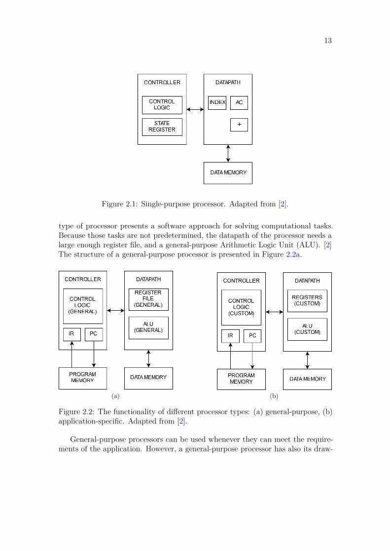
2.1 Single-purpose processorsA single-purpose processor is designed to execute only one program. It is simply acustom digital circuit used for one purpose. Another name for this type of circuitis an accelerator, or just "hardware". The program is hardwired directly to thecontrol logic and cannot be changed. [2] Figure 2.1 illustrates an architecture of asingle-purpose processor.
Accelerators can execute computational tasks more efficiently than general-purpose processors. A good example of a task is a video codec which uses analgorithm to compress and decompress the frames of a video. For a specific task,an accelerator has better performance, smaller size and lower power consumptioncompared to a general-purpose processor. However, its design time and Non-Recurring Engineering (NRE) costs are higher for small quantities, while theflexibility remains low. [2]
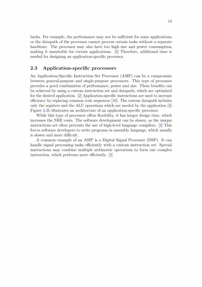
2.2 General-purpose processorsA general-purpose processor is designed for variety of applications to maximizethe number of sold devices. It executes user-written programs that are stored inthe program memory. A Program Counter (PC) is used to point to the programmemory location that stores the current or future instruction. An InstructionRegister (IR) is then used to hold the instruction which is being executed. This
13
Figure 2.1: Single-purpose processor. Adapted from [2].
type of processor presents a software approach for solving computational tasks.Because those tasks are not predetermined, the datapath of the processor needs alarge enough register file, and a general-purpose Arithmetic Logic Unit (ALU). [2]The structure of a general-purpose processor is presented in Figure 2.2a.
(a) (b)
Figure 2.2: The functionality of different processor types: (a) general-purpose, (b)application-specific. Adapted from [2].
General-purpose processors can be used whenever they can meet the require-ments of the application. However, a general-purpose processor has also its draw-
14
backs. For example, the performance may not be sufficient for some applications,or the datapath of the processor cannot process certain tasks without a separatehardware. The processor may also have too high size and power consumption,making it unsuitable for certain applications. [2] Therefore, additional time isneeded for designing an application-specific processor.
2.3 Application-specific processorsAn Application-Specific Instruction Set Processor (ASIP) can be a compromisebetween general-purpose and single-purpose processors. This type of processorprovides a good combination of performance, power and size. These benefits canbe achieved by using a custom instruction set and datapath, which are optimizedfor the desired application. [2] Application-specific instructions are used to increaseefficiency by replacing common code sequences [10]. The custom datapath includesonly the registers and the ALU operations which are needed by the application [2].Figure 2.2b illustrates an architecture of an application-specific processor.
While this type of processor offers flexibility, it has longer design time, whichincreases the NRE costs. The software development can be slower, as the uniqueinstructions set often prevents the use of high-level language compilers. [2] Thisforces software developers to write programs in assembly language, which usuallyis slower and more difficult.
A common example of an ASIP is a Digital Signal Processor (DSP). It canhandle signal processing tasks efficiently with a custom instruction set. Specialinstructions may combine multiple arithmetic operations to form one complexinstruction, which performs more efficiently. [2]
15
3 Processor design
3.1 Design objectivesThe general design goals for the processor are listed in Section 1.1. They areused to define the characteristics which the processor should have. However, anapplication-specific processor is designed for a special application or task. Therefore,the intended task defines the instruction set of the processor.
For testing purposes, the task for the ASIP is to serve as a main processor for aVGA graphics controller. Together they form a design that can be tested on anFPGA development board.
The graphics controller uses hardware accelerators to draw lines, circles orellipses, and to paint certain areas. A line can be drawn by knowing the x andy coordinates of its initial and end points. To create three-dimensional (3D)objects, the lines need to be calculated in three-dimensional space, which involvescomputations of trigonometric functions. To calculate those functions accuratelyenough, the processor must be able to do addition, subtraction and multiplicationwith 32-bit signed fixed-point numbers. Additionally, the multiplication has toinclude a built-in result selection for selecting the correct result from the output ofthe multiplier.
The graphics controller is operated directly with control signals from the pro-cessor. To generate the control signals, some special instructions are designed forthe instruction set of the ASIP. In this way, the graphics controller serves as anapplication-specific testing hardware for the ASIP. The implementation of thegraphics controller is examined in Section 4.6.
3.2 Memory architectureThe design process starts by defining the memory architecture of the processor.We know that an ASIP needs memories for both program and data. The memoryhierarchy of a computer system can be solved in two basic ways. In von Neumannarchitecture, both the program and data are placed in the same memory space. InHarvard architecture, they are located in separate memories. A modified Harvardarchitecture is a common solution in modern microprocessor designs. It containsaspects of both Harvard and von Neumann architectures. [14]
Since the goal is to design a soft ASIP processor, it is justifiable to choose theHarvard architecture. In this way, the processor does not have to use the sameaddress space, and arrange the bus access between the program and data memories.Options for the memory hierarchy are shown in Figure 3.1.
The used program memory needs to be a Read-Only Memory (ROM), as it isnon-volatile. The ASIP has a requirement of compatibility, thus it must operate
16
(a) (b)
Figure 3.1: Two memory architectures: (a) Harvard, (b) von Neumann.
with different types of memory configurations. Therefore, the program memory canbe either synchronous or asynchronous. The data memory is a normal RandomAccess Memory (RAM). Unlike the program memory, the RAM is volatile. To savethe contents of the RAM, an additional non-volatile memory such as an ElectricallyErasable Programmable ROM (EEPROM) could be used to store important datawhile the processor is powered off.
3.3 Datapath design3.3.1 Program counter
A generic computer datapath includes a program counter (PC) which is a registerpointing to the program memory [2]. The program counter holds the address ofthe current instruction. The next instruction can be fetched by incrementing thePC by one. Similarly, control operations can be implemented by manipulating thecontents of the PC.
The program counter is directly connected to the address line of the programmemory. Therefore, the bit width of the program counter defines the size of theprogram memory.
3.3.2 Program stack
A subroutine contains a sequence of instructions that perform a given task. Subrou-tines can be called multiple times in different locations of the program. They are apowerful programming tool for reducing the amount of maintainable code. [16]
Subroutines are normally implemented using subroutine calls. A subroutinecall includes a branching to the address of the subroutine. At the same time, thereturn address of the next instruction (PC + 1) is stored on top of a stack memory.This type of memory allows subroutines to call other subroutines (nested calls),and to also call themselves (recursive calls). [17]
17
In general-purpose processors, a stack memory can also be accessible by theprogrammer to ease the programming of some complex tasks. This is done withseparate PUSH and POP instructions. [16] However, the ASIP needs only theability to execute subroutines. Therefore, the processor needs a stack memorywhich is connected directly to the program counter. This type of implementationis often called as a program stack [13]. The subroutine calls are operated withCAL instruction, which pushes the return address on Top Of the Stack (TOS)and increases the Stack Pointer (SP) by one. Returning is done with the RETinstruction, which decreases the stack pointer by one and moves the TOS to theprogram counter. Moreover, the program stack cannot be accessed by any otherinstruction which makes it secure.
The depth of the program stack can be an issue if the number of nested orrecursive calls is high. The program complexity defines the suitable depth of thestack. As the ASIP is going to support a very large program memory, the depthof the stack needs to be great enough to minimize the risk of a stack overflow.A 32-level program stack can be considered large enough for our test software.However, it is the programmer’s responsibility to ensure that the stack does notrun out.
3.3.3 Registers
To store the results of the ALU, at least one accumulator (AC) register is required.The accumulator is also physically connected to one of the ALU inputs. An otherway for storing the ALU result is the use of a register file. This is common practicefor example in a MIPS datapath [18]. However, as explained in Section 2, an ASIParchitecture includes only the registers that are necessary for the purpose of theapplication.
For addressing data memory indirectly, the content of a memory location canbe used to point a memory address. Typically, the contents of a register file canbe used as pointers for indirect addressing. [16] To save resources, the ASIP doesnot need a register file, as it needs only the registers that are necessary for theintended task. Because of that, a single register is enough to implement indirectaddressing. This so-called file register (F) can be loaded from the accumulator withits own instruction. To load or store data indirectly, two separate control signalsare needed. They are used to control the addressing mode multiplexer which isshown in Figure 3.2.
The rest of the implemented registers are application-specific. The graphicscontroller requires three output registers (X, Y and OUTPUT). They could beloaded through the accumulator, but it is more efficient to load them directly fromthe data memory.
18
Figure 3.2: Addressing mode multiplexer.
3.3.4 Data bus
A data bus combines all registers, memories and an Arithmetic Logic Unit (ALU).A design objective for the ASIP is to handle 32-bit signed fixed-point numbers.If the width of the bus would be for example 8 bits, adding two 32-bit integerswould take a number of instructions. The ALU would have to also use a carry bitto produce the correct results. As the ASIP does not use a register file, processinglarge numbers would result very complex programs with a lot of load and storeoperations. For these reasons, it is reasonable to use a 32-bit data bus.
Respectively, all the registers, memories and the ALU have the same width asthe data bus. However, the address lines of the program and data memories use adifferent bus width, because these lines also determine the sizes of those memories.
3.3.5 Arithmetic logic unit
An Arithmetic Logic Unit (ALU) performs all the arithmetic operations of a CPU.The structure of an ALU consists of two inputs and an output for the data. Therecould also be input and output for a carry bit. In processors, the carry bit istypically saved in a carry flag of a status register. [19] However, storing the carrybit is not always needed if the data bus is wide enough for executing all arithmeticoperations directly. In addition, some microprocessors even have instructions toexecute ALU instructions without the carry [18].
The ASIP needs only normal arithmetic and bitwise operations, because manyoperations as negation or two’s complement, can be done as a combination ofthose instructions. Any operation that is not absolutely necessary is better leftout to save logic resources. The ALU has also one application-specific operationwhich is the 32-bit multiplication with built-in result selection. This operation isperformed using a 32-bit multiplier with a 64-bit output. The result selection isneeded to select the 32-bit signed fixed-point number from the multiplier output.
19
The designed ALU operations for the ASIP are shown in Table 3.1.
Table 3.1: 32-bit ALU operations.
Operation Formula DescriptionBYPASS F = B ALU bypassADD F = A + B Addition without carrySUB F = A − B Subtraction without carryMUL F = (A ∗ B)[55:24] Multiplication with result selectionAND F = A ∧ B Bitwise conjunctionOR F = A ∨ B Bitwise disjunctionXOR F = A ⊕ B Bitwise exclusionINC F = A + 1 IncrementDEC F = A − 1 DecrementCIL F = A ≪ 1 Circulate leftCIR F = A ≫ 1 Circulate right
One design goal for the ASIP is to have high performance. This is achieved byusing a clock frequency which is as high as possible. Figure 3.3 shows a digitalsystem for timing analysis of the ALU. It consists of two Flip-Flops (FFs) whichare connected together through the combinational logic of the ALU.
Figure 3.3: Timing model of the ALU.
The minimum clock period, Tmin of digital system is defined as
Tmin = Tclk−q + Tlogic + Tsetup − Tskew (3.1)
where Tclk−q is the clock-to-Q delay, or the delay from clock arrival until dataarrives at the Q of the flip-flop; Tlogic is the propagation delay of the ALU; Tsetup
is minimum time data must arrive at D before the next clock edge occurs (setuptime); and Tskew is the propagation delay of the clock between the two flip-flops
20
[20]. The maximum allowable clock frequency [20], Fmax is then defined as
Fmax = 1Tmin
. (3.2)
From Equation 3.1, it can be seen that the Tlogic is a key factor which affectsthe Fmax in Equation 3.2, because the propagation delay of many ALU operationsis significantly long. The ALU is also the only component of the datapath withlarge amounts of combinational logic.
For achieving the shortest possible Tlogic, all ALU operations are executed inparallel. The result is then selected by a multiplexer which has a select line calledALU SEL. A structure of the designed ALU is shown in Figure 3.4. The 32-bitmultiplication is presumably the slowest of the ALU operations, as it consists of anarray multiplier or other delay adding multiplier design. However, it is possibleto reduce the delay by pipelining the multiplier design, which is presented in theSection 4.5.4.
Figure 3.4: Design of the ALU.
3.3.6 Datapath organization
All the declared components can be connected together to create a completedatapath of the ASIP. The ASIP needs enough memory for running complexprograms and for storing data. However, the memory sizes cannot be static as one
21
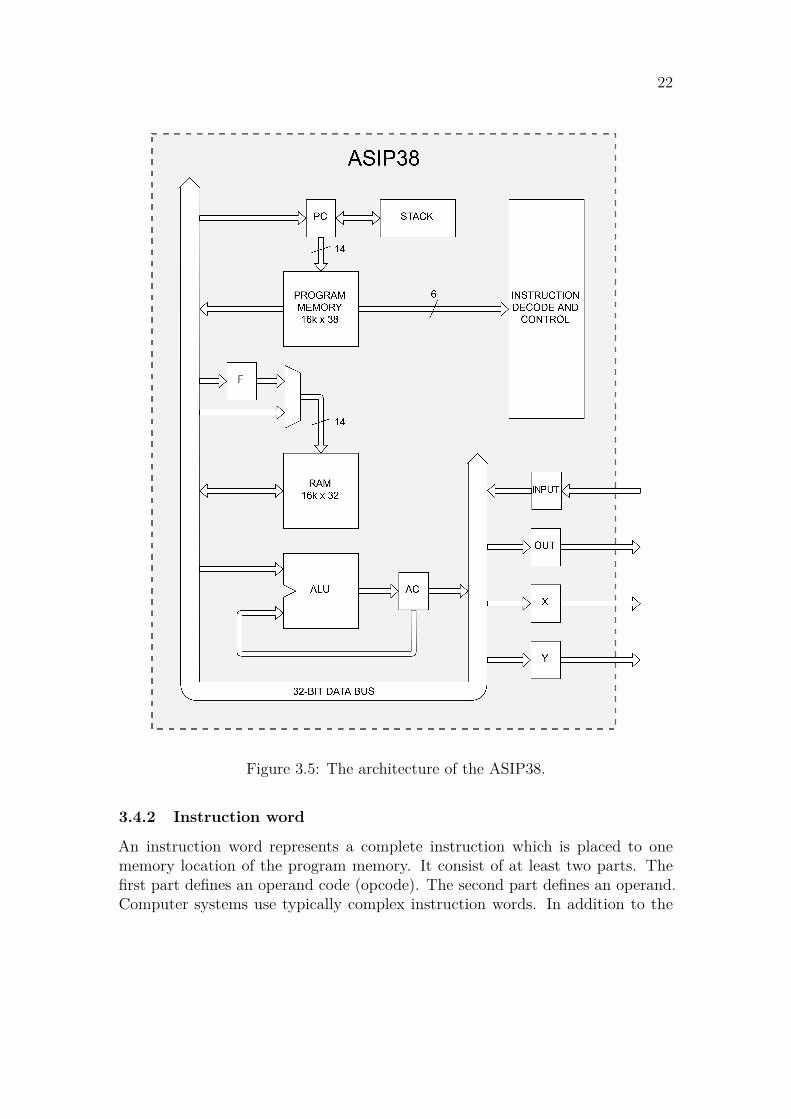
design goal of the ASIP is to be easily customizable. Given the selected 32-bit databus, the ASIP supports directly a memory size of 232. Therefore, the design of theASIP does not limit the size of memory for any practical applications.
In the Figure 3.5, both address buses have the size of 14 bits. The sizes ofthe program and data memories are exactly 214 which is equal to 16 384 memorylocations. As the amount of memory is defined by the width of the data bus, themaximum memory size for both of the memories is 232. As the width of the programmemory is 38 bits, the designed processor can be appropriately called as ASIP38.
Figure 3.5 shows the register level organization of the ASIP38 which is alsoknown as an architecture. The figure shows also a control unit (Instruction decodeand control). Its operation is described in the following subsections.
3.4 Instruction set architecture3.4.1 Overview
An Instruction Set Architecture (ISA) describes to the design of a computer, and isoften referred as computer architecture. It describes the computer operations whichthe ASIP38 will support. Instruction set architectures are normally characterizedinto two main categories. In Reduced Instruction Set Computers (RISC), allinstructions fit in a single word. A RISC processor also uses load/store architecturewhere the data memory is accessed only with load and store instructions, and allarithmetic operations must be executed in the registers of the processor. Simpleaddressing modes are also typical for RISC systems. As a result, a RISC instructionset has fewer instructions compared to more complex ISAs. [16]
Another category for an ISA is called Complex Instruction Set Computer (CISC).In CISC processor, an instruction can use more than one instruction words. Inthis way, a single instruction supports multiple operations or addressing modes.This allows the execution of complex tasks with only one instruction. A CISCarchitecture allows applying arithmetic operations to both memory and registeroperands. Therefore, a CISC does not have to use load/store architecture to accessthe memory, which is a key difference compared to RISC systems. [16]
As the ASIP38 is an application-specific processor, it needs to implement only thenecessary instructions. As the processor needs also to have a small implementationsize, the number of instructions must be low. The processor has a requirement ofbeing easily customizable, which can be achieved by fitting the instructions in asingle word and having simple addressing modes. Consequently, the ISA of theASIP38 will be designed from a RISC perspective.
22
Figure 3.5: The architecture of the ASIP38.
3.4.2 Instruction word
An instruction word represents a complete instruction which is placed to onememory location of the program memory. It consist of at least two parts. Thefirst part defines an operand code (opcode). The second part defines an operand.Computer systems use typically complex instruction words. In addition to the
23
opcode, the word can contain fields for register access, addressing modes or otherfeatures. [19]
The opcode is the identifier of the operation in the instruction, whereas theoperand defines the addressing mode. The ASIP38 needs only two addressingmodes to operate. In a direct addressing mode, the operand is a direct address ofthe data memory. In an immediate addressing mode, the operand is a literal valuewhich can be transferred to the accumulator, or other register. Bit numbering ofthe opcode and the operand start at zero for the Least Significant Bit (LSB). Table3.2 shows the 38-bit instruction word.
Memory operations can be separated into direct and indirect types. Direct opera-tions have the RAM address within the instruction word.
All load and store operations are performed through an accumulator (AC)register. The AC is loaded from the RAM memory with the LDA instruction.Accordingly, the content of the AC is stored to the RAM using the STO instruction.Other memory related instructions are arithmetic or bitwise operations. Theseoperations are performed between the RAM and the AC, and the result is naturallystored back to the AC.
Indirect addressing is necessary as it makes possible accessing the memory withthe result of an arithmetic operation. The easiest way of doing this is with separateaddress register that points to the memory indirectly. There are many ways toimplement indirect addressing but a straightforward way is to design separateinstructions for it. This also simplifies the instruction decoding.
To address the RAM memory indirectly, a file register (F) is needed. To accessthe RAM using the F register, three new instructions are introduced. InstructionLFR reads the RAM contents indicated by the F register to the AC. InstructionSFR stores the contents of the AC to the RAM location indicated by the F register.Finally, instruction WFR writes the contents of the AC to the F register. Memoryrelated instructions are shown in Table 3.3.
24
Table 3.3: Memory instructions.
Mnemonic Opcode Operation DescriptionLDA 000001 AC ← RAM[A] Load AC from RAMSTO 000010 RAM[A] ← AC Store AC into RAMADD 000100 AC ← AC + RAM[A] Add AC to RAMSUB 000101 AC ← AC − RAM[A] Subtract RAM from ACMUL 000110 AC ← AC ∗ RAM[A] Multiply AC by RAM (res. sel.)AND 000111 AC ← AC ∧ RAM[A] AND RAM with ACIOR 001000 AC ← AC ∨ RAM[A] OR RAM with ACXOR 001001 AC ← AC ⊕ RAM[A] XOR RAM with ACLFR 011110 AC ← RAM[F] Load AC from RAM indirectlySFR 011111 RAM[F] ← AC Store AC into RAM indirectlyWFR 100000 F ← AC Write AC to F
3.4.4 Accumulator operations
The second group of operations is related to the contents of the accumulator.Accumulator operations do not include reading or writing to the RAM. The mostimportant instruction is LDI, which is used to move immediate to the AC. Thisoperation is vital as the RAM is clear after every power-up. Without LDI, movingdata to RAM is not possible. Other useful instructions include INC and DEC,which are used to increase or decrease the accumulator by one.
Bitwise operations are often required to modify numbers, or for multiplicationand division. Thus, shift instructions CIL and CIR are needed. They are usedfor shifting the contents of the accumulator bit by bit to the left, or to the right.Sometimes no operation (NOP) is also necessary to enable an empty operation intime-critical programs. However, it can be replaced by other operations.
An accumulator value can be used for controlling the program flow. Basicoperation is to skip next instruction depending if the accumulator value is zeroor non-zero. For example, the SNZ instruction skips the next instruction if thevalue of the accumulator is non-zero. Accumulator related instructions are shownin Table 3.4.
3.4.5 Input/Output operations
Input/Output (I/O) operations are essential for communicating with externaldevices. An input instruction INP is needed to obtain data from the INPUT
25
Table 3.4: Accumulator instructions.
Mnemonic Opcode Operation DecriptionLDI 000000 AC ← immediate Load AC with immediateINC 001010 AC ← AC + 1 Increment ACDEC 001011 AC ← AC − 1 Decrement ACCIL 001100 AC ← AC ≪ 1 Circulate AC leftCIR 001101 AC ← AC ≫ 1 Circulate AC rightSNZ 010011 PC + 2 if AC ̸= 0 Skip if AC is not zeroSZA 010100 PC + 2 if AC = 0 Skip if AC is zeroSGT 010101 PC + 2 if AC > RAM[A] Skip if AC is greater thanSLT 010110 PC + 2 if AC < RAM[A] Skip if AC is less thanSKI 010111 PC + 2 if INPUT = 0 Skip if INPUT is zero
register, and to store it to the RAM address indicated by the instruction word.The processor has three output registers: X, Y and OUTPUT. They are directly
connected to the graphics controller. Instructions LDX, LDY and OUT are usedto store data into the registers. These registers are loaded directly from the RAMto make programming more efficient.
Two application-specific instructions are implemented for sending commandsto the graphics controller. Instruction SET controls MODE register which storesthe command provided by the instruction word. It also triggers control signalDISP_SET which enables the graphics controller to execute the given command.Instruction CLR is required for clearing video memory locations without affectingthe contents of the MODE register. All I/O related instructions are shown in Table3.5.
3.4.6 Control operations
Control operations are used to control the flow of a program. The most commoncontrol operation is to branch unconditionally or with some condition. The condi-tions are usually accumulator related. At the minimum, an unconditional branch(JMP) instruction is needed.
The graphics controller includes hardware accelerators which require someprocessing time. During the time, the graphics controller is unable to receivecommands from the processor. Therefore, the processor must wait until thegraphics controller has performed its current task. For the wait operation, WAIinstruction is implemented. The WAI instruction halts the processor if the value of
26
Table 3.5: I/O instructions.
Mnemonic Opcode Operation DescriptionINP 010001 RAM[A] ← INPUT Store INPUT into memoryOUT 010010 OUTPUT ← RAM[A] Load OUTPUT from memoryLDX 001111 X ← RAM[A] Load X from memoryLDY 010000 Y ← RAM[A] Load Y from memorySET 011000 MODE ← immediate Command to graphics controller
the READY flag is 0. The operation of the processor is continued when the flagreturns to 1.
A subroutine call has direct control of the program stack. Therefore, instructionCAL is introduced which stores the return address (PC + 1), increases the stackpointer and stores the address of the subroutine to the program counter. Returningfrom subroutine also needs its own RET instruction, which decreases the stackpointer, and places the output of the program stack to the program counter. Controlrelated instructions are shown in Table 3.6.
Table 3.6: Control instructions.
Mnemonic Opcode Operation DescriptionJMP 000011 PC ← address [A] Unconditional branchWAI 001110 Wait if READY = 0 Conditional waitCAL 011010 STACK[SP] ← PC + 1 Call subroutine
SP ← SP + 1PC ← address [A]
RET 011100 SP ← SP − 1 Return from subroutinePC ← STACK[SP]
27
3.5 Instruction cycle3.5.1 Single-cycle approach
In a single-cycle processor, the instruction is fetched, decoded, executed and itsresults are stored back to the memory in a single clock cycle. The length of theinstruction cycle defines the longest possible propagation delay of the processor.The longest possible delay path is called the critical path, which is equal to theworst-case delay for all instructions. [18] It determines the minimum clock periodTmin which can be used.
Single-cycle processors can be difficult to implement for an FPGA if externalmemory resources are used. For example, many Block RAMs have too much readand write latency to be used in a single-cycle processor [21]. For these reasons, amulti-cycle approach is a better solution for the ASIP38.
3.5.2 Multi-cycle approach
In single-cycle processors, data must propagate through the processor in a singleclock cycle, which means that minimum clock period Tmin needs to be fairly long totake care of the propagation delay. Multi-cycle processors use multiple clock cyclesto complete a single instruction. In this way, signals need to travel less distance ina single clock cycle, which allows to shorten the minimum clock period [19]. Figure3.6 demonstrates the gained performance in a multi-cycle design.
Figure 3.6: Comparison of instruction cycles: single-cycle and multi-cycle.
Typically, an execution of an instruction requires at least five clock cycles.Classic RISC pipeline is a good example of a five cycle design with following stages:Instruction Fetch (IF), Instruction Decode (ID), Execution (EX), Memory access(MEM) and Write-Back (WB) [22]. It is shown in Table 3.7.
28
Table 3.7: The five stages of the classic RISC pipeline.
Stage DescriptionIF Instruction fetch. Increment PC.ID Instruction decode. Read registers.EX Execution. Calculate effective address.MEM Memory access using effective address.WB Write the result into the register file.
The five stages of the classic RISC pipeline is a good model for the instructioncycle of the ASIP38, with a few exceptions. Firstly, the ASIP38 has no need tocalculate effective addresses, because it does not use a register file to address thedata memory. Secondly, the program counter needs to be updated before theinstruction is fetched. In this way, the program counter needs to be updated onlyonce per instruction cycle, reducing the complexity of the control unit.
Without the need for effective address calculations, the instruction cycle of theASIP38 can have only four stages. To keep things simple, every instruction of theASIP38 will be processed in four clock cycles. This is also a common practise, forexample, in PIC microcontrollers [23].
To optimize the clock speed to be as fast as possible, it is important to keep thethe critical path of each stage as short as possible. To achieve this, it is importantto organize all datapath operations into the correct stages. The main principle isto use multiple inexpensive operations, or to use one expensive operation per oneclock cycle.
Inexpensive datapath operations are usually those where the propagation delayis small. For example, registers or multiplexers have fairly small delay. Respectively,an ALU operation or a memory access has a much longer delay, and is better tobe executed apart from other operations. This happens by restricting reading andwriting of the memory or the accumulator to corresponding stages.
The following four stages define the instruction cycle of the ASIP38. The Fetchstage is reserved for updating the program counter and fetching a new instructionfrom the program memory. In the Decode stage, the instruction is decoded andcorrect register/memory is selected to the data bus. The Execute stage performsan ALU operation and generates all instruction-specific control signals. Finally,the MemWrite stage writes the result back to selected register/memory, and selectsa new operation for the program counter. The suggested four stages are shown inTable 3.8.
With the above four stages, four clock cycles are used per instruction. Thus,
29
Table 3.8: The four stage instruction cycle of the ASIP38.
Select register/memory to data bus.Execute Execute ALU operation. Generate rest of the control signals.MemWrite Write the result to the register/memory. Select PC operation.
the Cycles Per Instruction (CPI) value for the ASIP38 is always 4. As mentionedin Section 1, the ASIP38 has a design goal for compatibility. An external RAMcomponent has a delay from the time a new address is entered, to the time thecontents of the memory are shown at the output of the RAM. This delay is wellsupported by the instruction cycle as the RAM address is updated in the Decodestage.
3.5.3 Pipelined approach
The ASIP38 has a requirement of high performance. An efficient way to improvethe performance is to use a pipelined instruction cycle. Pipelining is a techniqueused to improve the performance of a processor by overlapping the execution ofinstructions [18].
Overlapping instructions can create what is called a hazard. Structural hazardsarise when the same part of the processor’s hardware is simultaneously needed bytwo or more instructions. A data hazard arise when an instruction has a dependencyon the result of a previous instruction and the data is exposed by the overlappingof instructions. Pipelining branch instructions can create a control hazard if theoutcome of the branch is not predicted beforehand. [18]
To anticipate all the hazards, a pipelined processor needs considerably moreadditional logic than non-pipelined processor. For this reason, it was decided touse a non-pipelined instruction cycle in the design of the ASIP38.
3.6 Control unit3.6.1 Structure
The control unit generates the control signals which control the datapath. Theprogram counter needs control signals for choosing the next PC operation, whetherit is incremented by a value, or loaded with an address for branching. Every register
30
and memory needs at least one control signal for writing. The ALU and the databus need control signals which have a multiple bit width.
A control unit can be designed in many ways. One option is to use combinationallogic, for example logic gates, encoders, decoders and multiplexers. In this way,the control logic can be minimized to use less resources, which is one of the designgoals in Section 1.1. If an instruction contains more than one cycles, this type ofdesign needs also a synchronous part to store the information of the current cycle.This type of design can also be problematic if later modifications need to be made.
The control unit can also use synchronous logic to generate the control signals.A Moore type Finite State Machine (FSM) can be used to implement a multiplestate instruction cycle [18]. It can be implemented with decoders and state registersas seen in Figure 3.7.
Figure 3.7: Control unit implementation with a Moore type FSM.
3.6.2 Control signals
Control signals are used for controlling the components of a datapath. In a single-cycle processor, the instruction is decoded and the required control signals aregenerated in one clock cycle. In a multi-cycle processor, the control signal generationis distributed over different stages of the instruction cycle.
A key part of the control unit is a control logic for the data bus. As seen fromTable 3.9, the control signal BUS SEL is generated in the Decode stage, and itremains the same until the next instruction. It controls a multiplexer, which selectswhat memory is selected to the data bus. The selected memory can be either theoutput of the program memory, data memory, accumulator or input register.
Control signals ALU SEL and MEM SEL are also generated in the Decodestage. The ALU SEL selects an ALU operation, and the MEM SEL selects a direct
31
Table 3.9: Generated control signal for each stages of the instruction cycle.
Control signal Fetch Decode Execute MemWriteBUS SEL x x x xALU SEL x x x xMEM SEL x x x xSTACK PUSH xSTACK POP xX LOAD xY LOAD xINPUT LOAD xOUTPUT LOAD xAC LOAD xRAM WRITE xPC SEL xWRITE F xOther signals* (x) (x) (x) (x)
* Application-specific instructions can have control signals at any ofthe stages.
or an indirect addressing mode for the data memory. Both control signals remainthe same for the rest of the instruction.
The Execute stage has the most of the control signals. The stack memory isoperated in this stage with the control signals STACK PUSH and STACK POP.The signals are generated by the CAL and RET instructions. It is possible tooperate the stack from other stages, because there are no strict timing requirementsfor dealing with the return addresses. The write operations of the X, Y, INPUTand OUTPUT registers has to be performed in the Execute stage, because the datamemory is automatically addressed by the instruction word in the Decode stage.
The MemWrite stage has the function of writing the results back to the accu-mulator, or the data memory. Signal AC LOAD is used to load the accumulator,and signal RAM WRITE operates the data memory. The next program counteroperation is selected with the PC SEL signal. The control logic of the PC isexplained in the next subsection. Control signal WRITE F is used to load the Fregister from the accumulator. Finally, application-specific control signals can begenerated in any of the stages.
32
3.6.3 PC control
The program counter is controlled by the select line PC SEL. It is generated in thecontrol unit as a result of the decoded instruction. Other factor that may affect tothe PC SEL signal is the status of the accumulator in the SNZ, SZA, SGT or SLTinstructions. The SKI instruction uses status of the INPUT register. Figure 3.8shows the logic controlling the program counter. The correct operation for eachinstruction is defined in Section 3.4.
Figure 3.8: PC control.
Figure 3.8 shows also the select line operating a multiplexer which controls theoperation of the program counter. The PC SEL is a 3-bit select line which includesfive control modes: PCLatch, PCInc, PCSkip, PCLoad and PCRET. These fivemodes perform all the necessary tasks for the whole instruction set. Mode PCLatchdoes not affect to the PC, mode PCInc increments the PC by 1, mode PCSkipincrements the PC by 2, mode PCLoad loads an address from the data bus intothe PC, and mode PCRET loads the PC with the Top Of the Stack (TOS).
The design of the control unit is ready, which also completes the processorarchitecture of the ASIP38. The next section describes how the architecture isimplemented in VHDL.
33
4 VHDL implementation
4.1 FPGA design flowThe implementation follows a process known as a design flow. The design could bealso implemented in Verilog HDL, but VHDL is chosen as it is a common languagein FPGA designs [24]. To prove that a design can be implemented physically,the design requires a target device. For prototyping, a Field-Programmable GateArray (FPGA) is a common option. An FPGA is a digital IC that can be easilyprogrammed to implement the functionality of any digital circuit. FPGAs aregenerally used in embedded systems and for prototyping. They have evolved in the1980s from earlier PLDs such as Complex Programmable Logic Devices (CPLDs)and Programmable Logic Arrays (PLAs) [25].
Alternatively, the target device could be an Application-Specific IntegratedCircuit (ASIC). While they are better in achieving optimal speed and powerconsumption, the NRE cost for a small amount of ASICs would be remarkablyhigh [2]. In our case, the only cost-effective option is to use an FPGA for testingand proving the final implementation.
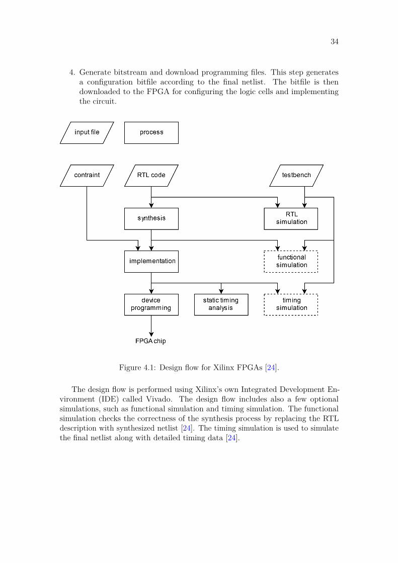
The target device we are going to use is a popular Xilinx FPGA. The detailsabout this device are explained in Section 4.2. The design flow for Xilinx FPGAsis shown in Figure 4.1. It consists of the following major steps [26] [27].
1. Design the system and produce Hardware Description Language (HDL) andconstraint files.
2. Develop a testbench in HDL and perform Register Transfer Level (RTL)simulation.
3. Perform synthesis and implementation. The synthesis process is where asoftware is used to transform the HDL to a generic gate-level representation.It is followed by the implementation process consisting of three mandatorysub-processes:
(a) The Opt Design optimizes the gate-level representation and makes easierto fit it onto the Xilinx target device.
(b) The Place Design produces the physical layout inside the FPGA chip.The logic cells are placed in physical locations.
(c) The Route Design step determines which wires should be used to connectthe placed logic cells to each other.
In the Xilinx design flow, static timing analysis is performed at the end ofthe implementation process. It determines various timing parameters, suchas the maximum propagation delay and the maximum clock frequency.
34
4. Generate bitstream and download programming files. This step generatesa configuration bitfile according to the final netlist. The bitfile is thendownloaded to the FPGA for configuring the logic cells and implementingthe circuit.
Figure 4.1: Design flow for Xilinx FPGAs [24].
The design flow is performed using Xilinx’s own Integrated Development En-vironment (IDE) called Vivado. The design flow includes also a few optionalsimulations, such as functional simulation and timing simulation. The functionalsimulation checks the correctness of the synthesis process by replacing the RTLdescription with synthesized netlist [24]. The timing simulation is used to simulatethe final netlist along with detailed timing data [24].
35
4.2 Artix-7 FPGA resourcesFor the final implementation, we select the Digilent Basys 3 FPGA developmentboard. The board has an Artix-7 series FPGA produced by Xilinx using a 28 nmmanufacturing processes. The part number of the FPGA is XC7A35T-1CPG236Cwhich has the following features [28].
• 33 280 logic cells in 5200 slices
• 1800 kbits of fast Block RAM
• Five clock management tiles, each with a phase-locked loop (PLL)
• 90 DSP slices
• Internal clock speeds exceeding 450 MHz
• On-chip analog-to-digital converter (XADC)
Additionally, the Basys 3 development board has the following features [28].
• 100 MHz oscillator
• 12-bit VGA output
• 16 user switches
• 16 user LEDs
• 5 user push-buttons
• 4-digit 7-segment display
• Four 12-pin Pmod ports
The Artix 7 FPGA provides 1800 kilobits of Block RAM which is essentialfor implementing the 16k program and 16k data memories for the ASIP38. Thegraphics controller, which we discuss later, also uses large amounts of Block RAM.The multiplier of the ASIP38 can be implemented with some of the hardwaremultipliers included in the DSP slices. From the development board itself, we aregoing to use the VGA output, and the five push-buttons. The Basys 3 developmentboard is shown in Figure 4.2.
36
Figure 4.2: Basys 3 FPGA development board.
4.3 Top level systemThe top level implementation consists of the VHDL codes of the ASIP38 processor,the input logic, and the graphics controller. Figure 4.3 describes the top levelsystem. The input block provides debounced button interface for the ASIP38 whilethe graphics controller is used to display the output. Its operation is explainedbriefly in Section 4.6.
Figure 4.3: Top level system.
37
4.4 Required VHDL packagesTo implement all the VHDL modules, it is necessary to use VHDL packages whichprovide all the necessary data types, operators and functions. When writing VHDLfor a synthesizable circuit, the package ieee.std_logic_1164 is usually required.It is essential as it provides std_logic and std_logic_vector data types includingtheir type conversions. An other important package is the ieee.numeric_std whichbrings two important data types: unsigned and signed. [29] Finally, we need theieee.std_logic_unsigned package which allows to treat std_logic_vector asunsigned and signed numbers [29].
4.5 ASIP38The VHDL implementation of the ASIP38 is provided in Appendix A.1. It consistsof one design file with multiple processes which implement the design. The entitydeclaration includes a set of port declarations. It contains all the input and outputsignals of the processor. For example, the system clock, and the input/outputregister connections are defined here along with some hardware specific controlsignals.
The internal registers of the processor are described as std_logic_vectortype of signals. They are introduced in the beginning of a design unit calledarchitecture.
4.5.1 Block RAM
Block RAM (BRAM) stands for Block Random Access Memory. It is a specialmemory module inside the FPGA device, apart from the logic cells. They are usedto implement large RAM or ROM memories inside the FPGA. [21]
The XC7A35T FPGA has 50 BRAMs. Each Block RAM has two independentports for simultaneous read and write operations and all memory operations arecontrolled by the clock. Each BRAM has the size of 36 kb, and it can be dividedinto two separate 18 kb BRAMs. A BRAM can be organized for different datawidths, for example from 16k x 1 to 512 x 36. [21]
The program memory of the ASIP38 takes (16k x 38) 622 592 bits, and thedata memory takes (16k x 32) 524 288 bits. Together they take up 1 146 880 bitsout of available 1800 kb, which is over half what is available.
An alternative for the BRAM would be to use distributed RAM which isconstructed from Look-Up Tables (LUTs). The LUTs are placed in a larger FPGAresource called slice. Each slice of the XC7A35T contains four LUTs and eightflip-flops, but only some of the slices can use their LUTs as a distributed RAM. The
38
maximum supported amount of distributed RAM is 400 kb which is not enough forthe ASIP38. [30] Therefore, it is better to use it for other purposes.
A BRAM, or a distributed RAM can be configured using Core Generator toolin the Xilinx Vivado software suite. Refer to Appendix A.1, page 68 for thedeclarations of program and data memories.
The data memory has two options for RAM configuration: single-port or dual-port. A dual-port RAM allows read and write operations at the same time usingtwo separate ports. [21] However, as the instruction cycle of the ASIP38 wasdesigned to be compatible for different memory configurations, it does not requirethe use of a dual-port RAM. Therefore, a single-port configuration is sufficient forthe RAM. The program memory has automatically a single-port configuration asit is a ROM.
Each memory has internal signals that need to be connected to the signals ofthe design file. In VHDL, this is done by using port maps. All connected memorycomponents must be declared in the beginning of the VHDL code. It is not possibleto use them directly, as they are located in a different file.
4.5.2 Program counter
The implementation of the program counter is provided in Appendix A.1, page70. The program counter is defined as a signal pc. For the control signal PC SEL,we introduce a user-defined enumerated data type pc_type. It is simply a list ofcharacter literals what the PC SEL can have. A signal pc_sel can be now definedto use the values of the pc_type.
The program_counter is a synchronous process, being only sensitive to theclock. The signal pc_sel can have the following values: PCInc, PCLoad, PCSNZ,PCSZA, PCSGT, PCSLT, PCSKI, PCRET, and PCLatch. All skip instructionscontrol the program counter directly, as the skip decisions are done inside theprocess.
4.5.3 Program stack
The program_stack is a synchronous process. It consists of stack, which is atwo dimensional array of std_logic_vector signals. As defined in Section 3.3.2,the size of the program stack is 32. The signal stack has its own type definitionstack_type. The stack has the signal stack_dataout for outputting the data.The program stack has also the signal stack_pointer which points to its addressline.
The program_stack process is controlled by two control signals: stack_push,and stack_pop. Their operation is to increment or decrement the stack pointer.It is not possible to decrement the stack when the stack pointer is zero. However,
39
if the stack pointer is incremented over the size of the stack, it goes back to zero.The implementation of the program stack is shown in Appendix A.1, page 71.
4.5.4 ALU
The alu of the ASIP38 is an asynchronous process which implements combinationallogic. Because of this, all input signals must be in the sensitivity list of the process.The ALU implements the following operations: bypass, ADD, SUB, MUL, AND,IOR, XOR, INC, DEC, CIL, and CIR. The bypass is used when loading to theaccumulator or when the instruction does not use the ALU. The implementationof the ALU can be found in Appendix A.1, page 71.
The XC7A35T FPGA has 90 DSP48 slices that are intended for Digital SignalProcessing (DSP) operations. A DSP48 slice contains one 25x18 multiplier. [30]The MUL operation uses four DSP48 slices to implement the operation for 32-bitmultiplication. It involves a built-in result selection for 32-bit signed fixed-pointnumbers. The multiplier is introduced in the beginning of the architecture as acomponent called mult32.
In the Section 3.3.5, the multiplier implementation was designed to be asyn-chronous. In this way, the MUL operation can be executed in one instructionstage which is practical to implement. However, this can cause too much logicdelay in the synthesis phase which can cause the failure of timing requirements.A good solution is to use enough pipeline stages in the multiplier. The processormust be then forced to wait for the result during the MUL instruction. This needsadditional control logic which is shown in Appendix A.1, page 77.
4.5.5 Instruction decode and control
Bus select
The content of the data bus is selected with the control signal BUS SEL. The databus has four different sources for data: the program memory output, accumulator,data memory output and input register. The BUS SEL is implemented in its ownasynchronous process called bus_select. It is shown in Appendix A.1, page 69.
Memory select
The selection of the data memory address could have been embedded directly to thecontrol logic itself, but it caused some additional slack which made the critical pathlonger. Therefore, the address for the data memory is selected by a multiplexer, asseen in Figure 3.2. It is operated by the control signal MEM SEL, which selects theprogram memory output or the F register into the address line of the data memory.The implementation of the multiplexer can be found in Appendix A.1, page 69.
40
State machine
The state_machine is a synchronous process which updates the signal state withthe next state of the instruction cycle. The process also implements the WAIinstruction based on the state of the ready signal. The implementation of the statemachine can be found in Appendix A.1, page 72.
Control logic
The control_logic is an asynchronous process which implements the instructioncycle of the Table 3.8. It generates all the control signals of the Table 3.9 accordingto the state signal. Control signals can use user-defined enumerated characterliterals or std_logic. In the beginning of the process, initial values are assignedfor the control signals that are not updated in the Decode stage. The control logicis constructed by using nested case statements, and its implementation is shown inAppendix A.1, page 72.
Resets
An essential VHDL design practise is to use reset signals inside the processes. BothASIC and FPGA designs need to have reset signals into registers in order to setan initial condition. However, modern FPGA designs can also use initial values inthe signal declarations. It is considered a good practice to reset as few flip-flopsas possible, and initialize all flip-flops instead as reset lines take routing resources.The reset lines also increase power consumption and make the design harder tomeet timing. [31]
As our target device is a Xilinx FPGA, we can benefit using initial values onsignals, and this way get lower resource usage, and optimal timing. To get the mostefficiency out of the design, resets should be coded only when they are necessaryfor the functionality of the design [32]. Therefore, the use of external reset signalsin our design is not necessary. For other target devices, the resets can be addedlater if needed.
4.6 Graphics controllerThe graphics controller is a test unit for the ASIP38. It is able to render vectorgraphics with a special line drawing algorithm. The main task of the ASIP38 is toact as a control processor by running a software that controls the graphics controller.The role of the graphics controller is to act as a platform for verifying and testingthe correct operation of the processor. It also helps testing the customizability andthe performance requirements of the ASIP38 as a part of a larger system.
41
Figure 4.4 shows a block diagram of the graphics controller. The graphicscontroller consists of three main VHDL modules which are the display controller,VGA synchronization and RGB signal generation. Figure 4.4 shows also othermodules, such as hardware accelerators, which are described later.
Figure 4.4: A block diagram of the graphics controller.
Display controller
The display controller is a command interface between the ASIP38 and the restof the graphics controller. It receives commands delivered by the SET and CLRinstructions of the ASIP38. A total of 29 different commands can be executed bythe SET instruction. The commands are used, for example, for changing betweengraphics modes, or writing to the video memory.
The display controller is connected to a paint memory which keeps track of thecontents of the display. This makes possible the flood fill algorithm to know whathas been written to the screen, as a video memory cannot be read directly fromthe display controller. The flood fill algorithm allows painting certain areas on the
42
screen. The implementation of the display controller is shown in Appendix A.2,page 78.
VGA synchronization
Video Graphics Array (VGA) is a graphics standard for display controllers firstintroduced by IBM Corporation in 1987. The VGA was designed at the time ofCathode Ray Tubes (CRTs). The color of a pixel is determined by the intensityof three components: Red, Green, and Blue (RGB). Each component can have avoltage level between 0 and 0.7 volts. [24]
The purpose of the module vga_sync is to produce timing for standard 640x48060 Hz video mode. The main clock for this mode is 25 MHz, which requires a clockdivider process vga_clk_25MHz. The timing for the electron beam is controlledusing signals for the horizontal and vertical synchronization (hsync, vsync). Theyare generated by counting the x and y pixel positions in processes called horizontaland vertical. The hsync makes the electron beam to start a new line, and thevsync to start a new frame. The signal video_on is used for switching the electronbeam off during a line change.
The x and y pixel positions are also used inside the process for the RGB signalgeneration. They are needed for reading the contents of a video memory. Theimplementation of the VGA synchronization is shown in Appendix A.3, page 84.
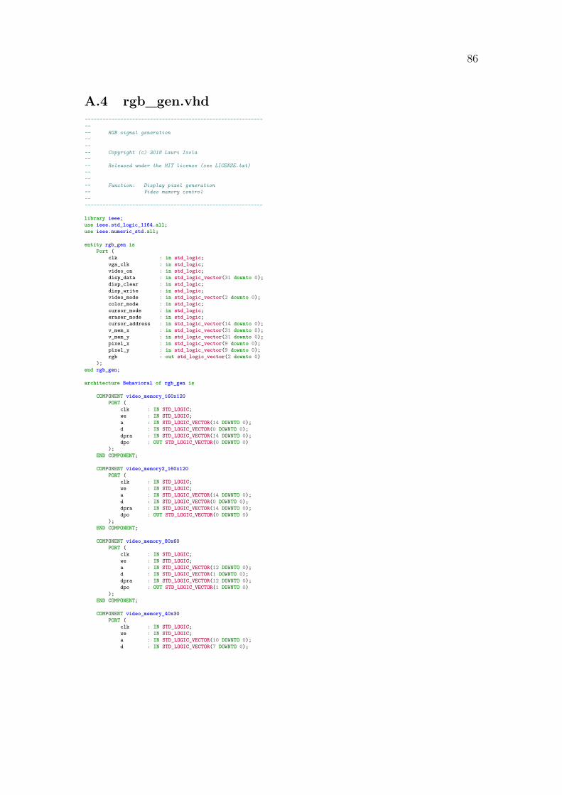
RGB signal generation
The RGB signal is generated using the contents of a video memory. Its implemen-tation is shown in Appendix A.4, page 86. The module rgb_gen outputs the RGBsignal which goes directly to the VGA connector. The graphics controller has fivevideo modes. As seen from Figure 4.4, each mode uses a separate video memory.The current video mode is selected with the signal video_mode.
The display consists of dots which can have a resolution from 160x120 down to40x15. The signals v_mem_x and v_mem_y provide the coordinate for a single dotthat can be set or cleared with the signals disp_write and disp_clear.
The RGB signal is produced by using signals pixel_x and pixel_y as a readaddress for selected video memory. The character code for the selected dot can bethen read from the output of the video memory. This code is used as a characteraddress for a font ROM. The output of the font ROM is then used to producepixels in true 640x480 resolution for the selected video mode.
Line drawing
The graphics controller uses module line_draw to generate lines in the videomemory. It is shown in Appendix A.5, page 91. The line_draw works as an
43
accelerator for the display_controller. Therefore, there is no need use anysoftware algorithm for line generation. This kind of hardware solution increasesthe overall performance and makes graphics programming easier.
The used algorithm is Bresenham’s line algorithm. It uses only integer numbers[33]. The module takes line start and end coordinates as inputs, and sends linecoordinates to the rgb_gen. The module is started with the line_start signal,and the video memory is updated with the line_update signal.
This module also manipulates the ready signal which is connected to the ASIP38.During line drawing the ready is 0 when otherwise it is 1. This makes possible touse the WAI instruction to prevent the execution of the ASIP38’s software duringthe time of the line generation.
Ellipse drawing
The module ellipse_draw generate shapes that include circles and ellipses. Theimplementation of the module can be found from Appendix A.6, page 94. Themodule works as an accelerator which is controlled similarly to the line_drawmodule. The module uses ellipse drawing algorithm which can be used to generateboth line and circles. It is based on Bresenham’s circle generating algorithm [34].
The required input parameters are x and y coordinates for the center of theellipse, and constants a and b. The ellipse generation is started using the signalellipse_start. The signal ellipse_update updates the video memory. Similarlyto the line drawing, this module also affects to the status of the ready signal.
Flood fill
The module area_paint is a fill tool for the graphics controller. It is an acceleratorwhich implementation is described in Appendix A.7, page 97. The module uses floodfill algorithm [35] to fill contained areas with the same color. The implementationof the algorithm is stack-based and works recursively.
The module takes the start location and color as its input parameters, andwrites its output directly to the video memory. The paint_memory is used forchecking the content of the display, as it is not possible to access the video memoryoutside of the module rgb_gen. Like the line and ellipse drawing, the area paintmanipulates the ready signal.
4.7 InputsThe Basys 3 FPGA board has five push-buttons that are needed for interactingwith the ASIP38. In the test setup, the states of these switches are used to interactwith the processor. However, using switches introduces phenomenon called switch
44
bounce. It occurs when a switch is pushed and begins to make a contact. Duringthat time the two contacts separate and reconnect usually 10 to 100 times over aperiod of about 1 millisecond [36]. During that moment, the state of the button isdifficult to determine.
A common solution is to implement switch debouncing, which waits until thebutton state stabilizes and then registers the state of the button. This methodcan be implemented in either hardware or software. [16] We select the hardwaremethod which uses a counter which increases when a button is pressed. The counterincreases in every clock cycle. When a specific count is reached, the button registersas pressed. Respectively, the counter decreases when the button is not pressed,and the button is registered as released when the counter reaches zero.
Push-buttons are asynchronous signal inputs which cause metastability to asynchronous system. To prevent metastability caused system failures, synchronizersmust be used between the push-button inputs and the rest of the system. For eachof the inputs, a synchronizer is implemented. It consist of a chain of at least twoflip-flops. [18]
The implementations of the debouncing and the synchronizers are shown in theinput module, which can be found in Appendix A.8, page 101. The input needsalso to produce a specific code for each button, or a combination of two buttons.Using button codes, the software knows which button or a combination is pressed.This is done with a synchronous process called button_select.
4.8 Top level entityThe module top connects other VHDL modules together to form the entire testsystem. It can be found in Appendix A.9, page 103. This system is connectedto the resources of the FPGA. The input signals of the system are the 100 MHzsystem clock (clk) and the five push-buttons: center, (btnC), right (btnR), left(btnL), down (btnD) and up (btnU). The outputs of the system are the VGAhorizontal synchronization (Hsync), vertical synchronization (Vsync), and threecolor intensity signals: vgaRed, vgaBlue and vgaGreen.
4.9 Behavioral simulationBehavioral simulation is an important part of the design flow. It is needed to verifylogical correctness of the RTL design. Before simulating any of the design files, aVHDL test bench needs to be created. The test bench is a separate file which isused to determine input values that are used during the simulation.
Behavioral simulation is an iterative process. It may take multiple simulationsto achieve the desired functionality. However, simulation is not very useful for
45
resolving problems with timing. For checking if the required timing conditions aremet, a static timing analysis is normally used [37].
Xilinx Vivado provides an in-built simulator which was used for verifying thedesired functionality. At first, the correct behavior of the ASIP38 was verified inthe simulator. This was performed using short test programs which tested the fullinstruction set. The correct operation of the datapath was then observed from thesimulation results.
During the development of the graphics controller, each design file was firstsimulated separately. However, the complete operation of the graphics controllerwas not simulated as verifying pure RGB signal is not practical enough.
After the correct operation was confirmed, the whole system was simulated.This was done to check for any errors during the simulation. These errors preventthe synthesis of the design, and must be corrected before continuing the designflow.
4.10 SynthesisSynthesis is the part of where VHDL code is converted into a gate-level netlist.The produced netlist is used in the implementantion phase to produce a placed androuted FPGA design. Xilinx Vivado uses a built-in synthesis tool for synthesizingthe design. It generates a synthesis report which contains useful timing information.
One of the design goals of the ASIP38 was the need for high performance. Tomeet that requirement, the processor should achieve clock speeds which are typicalfor the selected FPGA. Therefore, we choose to use the 100 MHz oscillator of theBasys 3 for the main clock of the system.
At first, the ASIP38 is synthesized alone without the graphics controller. Thisgives us a timing report that estimates if the processor passes all the timingconstraints. The obtained timing summary is presented in Table 4.1.
The term slack indicates the margin by which a timing requirement is met.Worst Negative Slack (WNS) refers to the worst slack of all the timing paths for
46
maximum delay analysis. If it is positive, the path passes. If negative, the pathfails. The Worst Hold Slack (WHS) refers to the worst slack of all the timing pathsfor minimum delay analysis. It must be positive to pass. Total Negative Slack(TNS) is the sum of all negative slack violations. It must be zero for meeting thetiming. Like the TNS, the Total Hold Slack (THS) is the sum of negative holdslack. It must also be zero for the design to pass. [38]
The timing summary, which is shown in Table 4.1, confirmed that the designpasses the static timing analysis. The maximum allowable clock frequency for theASIP38 can now be estimated using the 100 MHz clock period and the WNS asshown in Equation 4.1 [39]. The result of over 112 MHz is promising, but we alsoknow that the implementation phase can reduce these values. Because the designis not too close to the 100 MHz limit, it is safe to continue to the implementationphase.
Fmax = 1Tclk −WNS = 1
10 ns− 1.143 ns = 112.905 MHz (4.1)
4.11 ImplementationAs mentioned in the Section 4.1, the implementation consists of three sub-processesbefore the bitstream for the FPGA can be generated. The processes are theOptimization Design (Opt Design), Place Design and Route Design. It is possibleto do optional optimizations between the sub-processes, but they are not necessaryas we want to implement the design for testing purposes only. After running theimplementation successfully, the summary of the timing analysis is presented inTable 4.2.
Table 4.2: Timing summary after the implementation.
As expected, the WNS has been reduced. This has en effect to the maximumallowable clock frequency of the ASIP38, as seen in Equation 4.2.
Fmax = 1Tclk −WNS = 1
10 ns− 0.680 ns = 107.296 MHz (4.2)
47
With the graphics controller and the input module included, the complete testsystem has a WNS of only 0.245 ns. The maximum allowable clock frequency ofthe test system is then 102.511 MHz. For the system to work, the clock periodmust be greater than or equal to the critical path.
The timing report also presents the 0.680 ns critical path for the ASIP38, whichoccurred between the program memory and the accumulator. It is caused by theBlock RAM, as some extra delay accumulates due to the long routing distances. Itis often possible to shorten these delays by selecting the retiming option from thesettings of the synthesis engine. This moves the registers around while maintainingthe original functionality [20].
The ASIP38 has a design goal of small implementation size. Table 4.3 showsthe FPGA resource utilization of the ASIP38. From the table, it can be clearlyseen this goal was successful as the number of used LUTs is only 573. The onlyhigh consumer is the Block RAM, but its amount can be changed according toneeds of the application. During the implementation a size of 8k was used for theprogram memory, and 16k for the data memory.
Table 4.3: FPGA resource utilization of the ASIP38. The utilization for thecomplete test system is noted in parenthesis.
Table 4.3 shows that the complete system took a lot more resources than theASIP38 alone. The larger design needs to use more routes. Because of this, thecritical path emerged inside the graphics controller. The implementation is nowcomplete, and ready for testing.
48
5 Verification and testingThis section focuses on testing the board-level behavior of the ASIP38. Thepurpose of the this type of testing is to verify the correct functionality of theASIP38. This section also focuses on the software development tools, which areneeded for programming the ASIP38. A series of test programs are then introduced,and their results are analyzed.
5.1 Hardware verificationHardware verification is a critical step in any RTL design as the implementationmust perform to its specification. Furthermore, the behavioral simulation or thestatic timing analysis cannot guarantee the correct operation of the design inside ofan FPGA. Hardware verification can involve compliance tests, or other importantparameters that must be met. It is typically done by simulating or prototyping. [40]The most practical method for us is the FPGA prototyping. Doing otherwise wouldrequire using some other hardware verification method, for example, UniversalVerification Methodology (UVM).
Xilinx Vivado provides different IPs for hardware debugging purposes [41]. Forexample, a logic analyzer core could be used for monitoring internal signals of theFPGA. For our needs, the graphics controller serves as an on-chip debugger by dis-playing the output signals of the ASIP38. The real-time output can also be quickerto verify compared to the debugger. The graphic controller has been independentlyverified earlier which is an essential requirement for successful verification of theASIP38.
The verification by prototyping involves board-level testing with a series of testsprograms, which are executed by the processor. The results are then displayedin real-time by the graphics controller. The program complexity should be closeto tasks the processor would be normally executing. If a test program displaysexpected output, it can be considered successful. Board-level testing provides alsoa practical way of proving that the VHDL design was synthesizable on an FPGA.
5.2 AssemblerThe processor can be programmed by creating instructions directly in machinelanguage and transferring them to the program memory. In the Block MemoryGenerator of the Xilinx Vivado, this is done by writing the program lines to a textfile in a hexadecimal format, and loading the contents of the file directly into theprogram memory.
However, programming in machine language causes a well known problemespecially with the target addresses of the branch instructions. For example, every
49
time a new line is added to the program, the target addresses of the JMP or CALinstructions are changed. The problem gets bigger the longer the program is.
A solution is to use a symbolic machine language (Assembly), and an assemblerthat coverts assembly code into machine code [18]. An assembler is practicallymandatory software tool in almost every computer system. Therefore, we mustimplement a custom assembler program to help the software development of theASIP38.
In an assembly language, labels are used instead of absolute numeric addresses.Therefore, all branch target addresses become relative. In an assembly instruction,the leftmost label represents the program line address, and the rightmost labelrepresents either a memory address or an immediate. The middle tag is reserved foran instruction. If an instruction is not a destination for a branch instruction, theleftmost label will be replaced by ’-’. Conversely, if an instruction does not containan address or other number, the rightmost label is replaced with ’-’. Dashes areneeded to allow the assembler to recognize an empty space. The assembly languageformat of the processor is shown in Table 5.1.
Table 5.1: ASIP38’s instruction format in assembly language.
The RAM locations can be addressed using an assembler directive which givesa numeric constant to a symbolic label. They can be used to point a single RAMmemory location. A commonly used name for this type of directive is EQU [42].For example, a constant TEST can be given a value of 2 as follows: TEST EQU 2.Since the TEST now corresponds to number 2, it can be used as a variable for a
50
RAM memory location. For example, - LDA TEST loads a number from the thirddata memory location into the accumulator.
The assembler works in two steps. At first, a table is created where the leftmostlabel of each instruction is given an index number. The table provides the addresswhere each of the labels are located. The second step produces the final hexadecimalcode based on the first table. At the same time, the rightmost labels are replacedwith the hexadecimal values. The operand codes are also replaced with predefinedhexadecimal values.
A hexadecimal instruction has 10 characters. Due to the processor’s 32-bitdata bus, the eight rightmost ones are reserved for the address/immediate. Thetwo characters to the left represent the 6-bit operand code. For example, theinstruction word 030000001a corresponds to a JMP instruction to the location 1aof the program memory.
The output file of the assembler is a complete binary file which can be readby the Block Memory Generator of the Xilinx Vivado. The file has the correctformat and header fields required by the Vivado. This accelerates the softwaredevelopment as the required format is produced automatically.
During testing, the performance of the implemented assembler appeared tobe fairly good. The compilation took only few seconds even when the code wasseveral thousand lines long. The Python source code of the assembler is shown inAppendix A.10, page 107.
5.3 Test programsThe ASIP38 is tested with a series of test programs which are loaded into theprogram memory. They are designed to test the whole instruction set of the ASIP38.The programs can be divided into two categories: those which do read an inputfrom the user, and those which do not. We are interested in programs which readuser input, as the behavior of this type of programs is not completely predetermined.They are more likely to reveal design flaws in the hardware.
The test programs can be either small or large. Smaller tests concentrate to onespecific processor component. For example, the correct operation of the programstack can be tested by calling subroutines from another subroutine, printing anoutput, and returning back to the starting point. These programs perform wellwhen the testing concentrates on individual features of the processor. However,they do not always cover everything, and it is reasonable to test the processor withprograms which use the full instruction set.
A practical way for hardware testing is to first use smaller test programs, andthen start writing larger test programs. Complex software usually combines severalsmaller tests into one entity. This provides a good alternative for verifying theoperation of the processor.
51
Normal instructions
A program called SNAKE was assembly coded for testing general operation, sub-routine calls, and indirect addressing of the ASIP38. Its functionality is close toa classic snake game. Another program called BRICKS was assembly coded inthe case something was missing in the SNAKE. The BRICKS is a typical bricksbreaking game, and more complicated than the SNAKE. During testing both theSNAKE, and the BRICKS operated correctly and without bugs. This suggestedthat the hardware of the ASIP38 was operating normally on the FPGA, and moretest programs could be written. Figure 5.1 shows the BRICKS in action.
Figure 5.1: The BRICKS program.
Application-specific instructions
To use the application-specific SET instruction in its full potential, a software calledPAINT was programmed. It allows drawing lines, ellipses, circles or using a free
52
hand. The line and ellipse drawing use the Bresenham’s algorithm as described inSection 4.6. It provides an eraser tool, and a paint bucket which uses the flood fillalgorithm. As the algorithms are implemented inside the graphics controller, theSET instruction was tested comprehensively. All commands of the SET instructionwere tested, which served also as a functionality test for the graphics controller.As a result, the graphics controller operated as intended in the PAINT software.Figure 5.2 shows the PAINT software in operation.
Figure 5.2: The PAINT program.
The MUL is an application-specific instruction of the ASIP38. It makes possibleto multiply signed 32-bit fixed-point numbers. Moreover, the MUL instruction hasa built-in result selection which was designed especially for a test program calledCUBE. The CUBE program is capable of 3D rendering by producing a rotatingcube in a middle of the screen. It allows the cube to be rotated around its x, y andz axes. The shape of a cube is constructed by rendering lines in three-dimensionalCartesian coordinate space. The direction and the speed of rotation are changeableby the user.
53
Each corner of the cube represents one point which x, y and z coordinates needto be updated every time the points are rotated around the origin. For example,the previous coordinates of x, and y are used to calculate new coordinates for onecorner, as shown in Equation 5.1 [43].
x′ = x cos θ − y sin θ
y′ = y cos θ + x sin θ(5.1)
In the Equation 5.1, trigonometry is used for calculating variables x′ and y′,which represent the new coordinate values being calculated. Variables x and yrepresent the previous values, and θ represents the angle of rotation [43]. Figure5.3 shows the rotation of x and y coordinates around the origin. The Equation 5.1can be then used to create a program which rotates the cube around its x, y and zaxes.
Figure 5.3: Rotating x and y coordinates around the origin by θ.
As the cube is rotated by using its previous coordinates, the precision of themultiplication must be high enough, or the cube will become distorted over time.A working solution is to use 32-bit signed fixed-point numbers where the fractionalpart is at least 24 bits long. Thus, the multiplication precision is high enough toprevent an accumulating error. To handle a fixed point multiplication result, theMUL instruction was designed to select the bits 55 to 24 from the 64-bit multiplieroutput.
54
Figure 5.4 shows the CUBE program in action. After continuous running ofthe CUBE program, no visible distortion was detected. This was a clear indicatorthat the software and the hardware operated correctly. This also confirmed thedesired behaviour of the full instruction set.
Figure 5.4: The CUBE program.
5.4 Board-level testingThe instruction set of the ASIP38 was tested thoroughly. Especially real-timetesting with longer test programs was found useful. Continuously running software,such as the CUBE program, also tested the overall system stability. As a result,no hardware flaws were detected during any of the test programs.
The testing indicates that the functionality of the ASIP38 can be successfullysynthesized on an Artix 7 FPGA with the clock speed of 100 MHz. However, furtherverification with an on-chip logic analyzer is recommended, as the performed testswere limited only to the real-time board-level scenario.
55
6 Analysis of resultsAfter successful implementation, the features of the ASIP38 can be analyzed. Atfirst, we wrap up the results of the design process which were described in Section3. After that, we compare the results to other open source processors with similarfeatures for getting a better overview of the results.
6.1 Results of the design processThe ASIP38 is an application-specific processor which has a 32-bit data bus forefficient operations between large numbers. It uses a Harvard memory modelfor straightforward connection of the program and data memories. The ASIP38categorizes as a RISC processor, as its instruction set is small, and the instructionsfit in a single word. Having only two addressing modes, as explained in the Section3.4.2, also supports the RISC classification. For saving resources, the design ofthe ASIP38 does not use a register file. The accumulator is the only register forprocessing data. This forces the arithmetic operations to be performed between thememory and the accumulator, which is a CISC property. This leads the ASIP38 toimplement the RISC only partially, which is a good compromise in terms of speedand low resource usage.
The ASIP38 uses a multi-cycle ISA, and is directly compatible with commonmemory blocks inside of an FPGA. This type of instruction cycle makes possiblethat no additional clock cycles are used for waiting the output of the memory, suchas the Block RAM. As a result, the ASIP38 has a true performance of only fourclock cycles per instruction. The features of the ASIP38 are presented in Table 6.1.
6.2 Processor comparisonOpenCores [11] is an online community for the development of digital open sourcehardware. Its website offers binary compatible clones of commonly used processorarchitectures. GitHub [12] is another popular website which is used for hostingopen source hardware projects. OpenCores provides a comprehensive list [44] ofopen source processors from the websites above. As shown in Table 6.1, we canselect a few well-known and similar-sized processors from the list, and comparetheir features to the ASIP38. Although they are not ASIPs, the comparison toexisting processor architectures helps to form an overview of the tasks the ASIP38would be suitable for. This also helps to evaluate how well the design goals inSection 1.1 were achieved.
Table 6.1 presents the features of a processor core called T65. The ISA of theT65 is directly compatible to the 6502 microprocessor which was developed byMOS Technology in 1975. This processor has an 8-bit data bus, one accumulator
56
and two index registers. [45] Unlike the ASIP38, the 6502 implements the programstack inside of the RAM. It also has 13 addressing modes which is a CISC feature.The implementation of the T65 uses only 575 LUTs [44] which is almost equal tothe ASIP38.
Table 6.1: The features of the ASIP38 compared to small open source processorcores.
ASIP38 T65 Light52 AVR Core PicoRV32Category: ASIP core uP core uC core uC core uP core
The next processor in the table is an 8051 compatible microcontroller core. TheIntel 8051 was developed by Intel in the early 1980s, and has been widely used forsmall scale embedded systems [16]. The 8051 has an 8-bit data bus, and a complexinstruction set. This particular 8051 core has also peripheral modules for timerand Universal Asynchronous Receiver Transmitter (UART). Its implementationsize is 1022 LUTs [44].
Table 6.1 shows also an ATmega103 compatible microcontroller core. It usesthe AVR RISC architecture developed in 1996. The ATmega103 uses a 2-stagepipeline which executes an instruction in a single clock cycle [46]. It has threeperipheral modules: two for timers and one for UART. With all the features, theresource consumption of this processor core is 2135 LUTs. [44]
The last processor in the table is the PicoRV32. It uses an open source ISAcalled RISC-V which has been developed in University of California, Berkeley. TheRISC-V was introduced in 2010 and has been increasing its popularity since then.[47] The PicoRV32 is described as a size-optimized RISC-V CPU. It uses a 32-bit
57
data bus and employs a non-pipelined version of RV32IMC ISA with 55 instructions[48]. As a result, the PicoRV32 uses only 725 LUTs [44].
A significant benefit of the listed processor architectures is their support forHigh-Level Languages (HLLs). This means that programs can be written not onlyin Assembly language, but in high-level programming languages such as C. Itmakes programming more efficient, and allows using programs which were writtenon a different hardware.
The ASIP38 uses 573 LUTs with three application-specific instructions. Al-though the ASIP38 is a 32-bit processor, its implementation size seems to beapproximately similar to the other processor cores listed in Table 6.1. Moreover,any of the listed processor cores do not support Wishbone or any other bus interface,which can increase the LUT count.
In general, the features of the ASIP38 seem fairly similar to the processorcores listed in Table 6.1. The key difference is that the listed processors were notoriginally designed to be customizable. Therefore, any later modifications, such asadding new instructions, can be difficult and time consuming. In ASIP38, addingnew instructions, registers and other hardware can be done easily, because its ISAwas designed to be customizable.
The comparison indicates that the ASIP38 can be proposed for a role wherea small application-specific processor is required. The next section discusses itsfuture upgrades and improvements.
58
7 Future upgradesIn Section 1.1, the structure of the designed processor was required to be customiz-able. This makes possible to develop the ASIP38 further by adding new features.The features can be either internal hardware of the processor or pure software tools.This section presents some suggestions for future work.
7.1 Additional hardwareInterrupts
The ASIP38 could be designed to have interrupts. This would allow interruptingthe current program by an urgent event which needs to be processed immediately.An interrupt would first push the current PC address to the top of the programstack. A flag would be then be set to prevent new interrupts during the executionof the current interrupt. A subroutine called an Interrupt Service Routine (ISR)would be then executed at the address which would locate at a fixed location inthe program memory [2].
The interrupts could be triggered either internally or externally. An internalinterrupt is typically triggered by a peripheral, for example a configurable timermodule. An external interrupt is triggered by the state of an input port. [14]
Enabling and disabling interrupts could be done by separate instructions, orusing a configurable register. Other peripherals, such as timer modules, would alsoneed their own control registers. For accessing the registers, new instructions wouldhave to be implemented.
Multitasking capability
Sometimes interrupts are not enough to perform a lot of tasks in real-time. Further-more, placing long and complex code inside of an ISR can block other parts of theprogram from being executed. Subroutines can also take a long time to complete,and other subroutines have to wait until one finishes. Therefore, one significantimprovement for the ASIP38 would be the ability to perform multitasking.
In a typical multitasking scheme, a Real-Time Operating System (RTOS) wouldshare processor time for all runnable tasks. Thus, even the most time consumingtasks can be run without disturbing the real-time execution of other tasks. Thismethod of saving processor time is called scheduling. [14]
An important part of any RTOS is a scheduler. It is responsible for decidingwhich task should be executed at any particular time. A preemptive scheduler isable to switch tasks by using a process called context switch. Its function is tosave the state of the current task, or thread. The context switch makes possible torestore the task, and resume its execution later from the same point. [14]
59
A context switch can be triggered, for example, by a timer interrupt. Thefunctionality of the context switch is located inside of an ISR which saves allregister values of the current task to the data memory. The processor’s registerswould be then loaded from the RAM with the values of another thread. As thePC value is also loaded, the switched thread continues from the same location asbefore.
In the case of the ASIP38, the PC, AC, and F registers need to be saved andloaded by the context switch. Thus, these registers must be accessible from theinstruction set. Three new instructions would be needed for saving and loadingfrom the PC, and loading from the F register.
7.2 Software toolsAn assembler is an important tool for low-level software development. However, anassembly language is strictly tied to the processor and the instruction set it wasdesigned for. A high-level programming language, such as C, provides a number ofbenefits. For example, it can be compiled to different microprocessor architectures,and it allows using code which is already available for other systems. [2] The Csyntax can be also a lot easier to read, which makes it better for complex programs.
The support for a high-level programming language would be beneficial forthe software development of the ASIP38. The first option would be to modifyits instruction set to support a suitable high-level language compiler. The secondoption would be to develop a program which translates the assembly code of anotherprocessor to the assembly code of the ASIP38. However, this might be difficultdepending on the differences in the instructions sets.
From both of the options, modifying the instruction set might be easier to do. Itonly requires adding the instructions and registers of another processor architecture,but at the same time it changes the architecture of the ASIP38 by some degree. Inboth cases, the application-specific instructions of the ASIP38 would still have tobe inserted manually into the assembly code.
Suitable compilers would be those which have the assembly language closest tothe ASIP38. For example, the C compilers of accumulator based 8-bit microcon-trollers could be used.
7.3 Bus protocolsAn on-chip bus is the key component of a SoC. It is used to connect differentsystem components including processors, memory, and peripherals. All communi-cation occurs on a unified bus architecture. [1] This has the benefit of connectingseveral IP components using one shared communication protocol. This subsection
60
investigates the connectivity of the ASIP38 to the most commonly available on-chipbus standards: AMBA, CoreConnect and Wishbone.
The Advanced Microcontroller Bus Architecture (AMBA) is an open bus speci-fication developed by the ARM Corporation. It was developed in 1995, and hasbecome the de facto standard for interfacing components in a SoC. It has evolved toits third generation and includes three variants: a low-bandwidth general-purposebus called Advanced Peripheral Bus (APB), a high-speed single-frequency buscalled Advanced High-performance Bus (AHB), and a high-speed multifrequencybus called AMBA Advanced Extensible Interface (AXI). [1]
The CoreConnect is a bus system from IBM Corporation. It was developedfor IBM’s PowerPC line of processors. Its functionality is similar to the AMBAbus. Its main variants include a low-bandwidth general-purpose bus called On-chipPeripheral Bus (OPB) and a high-speed single-frequency bus called Processor LocalBus (PLB). [1]
The Wishbone is an open source bus system developed by the SiliCore Cor-poration [1]. It is used by many designs in the OpenCores [11] website. Thespecification defines master and slave interfaces which can be used to form differentbus topologies, such as point-to-point, many-to-many or even crossbar switches[49].
All of the bus system could provide a communication protocol for the ASIP38to exchange data with external IP blocks. However, the ASIP38 was developedfrom an open source perspective, and it is likely to be used in an open sourceproject. In the OpenCores, the IPs are usually made compatible with the Wishbone.The Wishbone is also simpler than AMBA or CoreConnect [1]. The OpenCoreswebsite also provides even a simplified version of the Wishbone called Simple BusArchitecture (SBA) [50]. The SBA implements a minimum subset of the Wishbone,and can be easily connected to other Wishbone compatible cores.
To connect the ASIP38 through a bus system, a custom bus adapter needs tobe designed. An adapter could be easily implemented to support the SBA, as itscore functionality is based on a FSM. Because of its reduced amount of logic, theSBA does not consume as much FPGA resources as the other bus systems. Thiscould be useful in the applications of the ASIP38.
61
8 ConclusionThe purpose of this thesis was to study the core knowledge and skills required toimplement an ASIP processor. The goal was achieved by designing and implementingan open source ASIP. The designed processor was named as ASIP38. It wasimplemented in VHDL for an FPGA target device. To test the ASIP38 in real-time,a VGA graphics controller was implemented using VHDL, which was connected tothe ASIP38 for creating a complete test system.
The design work was divided into five main goals. At first, the structure ofthe processor needed to be customizable, as this is an essential feature of an ASIPprocessor. The Instruction Set Architecture (ISA) of the ASIP38 was designedto have many characteristics from a RISC ISA. For example, instructions hadto fit in a single word, and the number of instructions were kept low. The RISCapproach allowed the processor to have only two addressing modes which makeslater modifications easier. The testing with the graphics controller also requiredthe design of three application-specific instructions.
The processor was required to be directly compatible with different memoryconfigurations inside of an FPGA. This ensured that many types of availablememory could be used, and the processor does not need to depend on just a singlememory configuration. This goal was achieved in the design of the instructioncycle.
The processor’s implementation size needed to be small. The goal was achievedby implementing only the necessary instructions and registers, instead of a complexinstruction set and a register file.
As the processor was required to be optimized for performance, the possibilityto have only one clock cycle per instruction was investigated. However, the single-cycle approach was not compatible with the Xilinx Block RAM. As a result, aninstruction cycle with four clock cycles per instruction was selected. A pipelinedinstruction cycle was also considered, but it would have made the design too complexfor the gained performance. A more feasible option was to increase the maximumclock frequency by keeping the critical path of the RTL design as small as possible.This helped to exceed the target clock speed of 100 MHz in the implementationphase.
The final goal was to make the processor user-friendly by providing the necessarytools for software development. The focus was set on implementing an assembler,as it is a crucial programming tool. The assembler implementation was a success,and the assembler was used for compiling test programs to binary code.
The VHDL implementation of the ASIP38 was first simulated using VHDL testbenches, and finally synthesised and implemented using the design flow for XilinxFPGAs. The implementation was then verified directly from an FPGA prototypeusing complex test programs. The programs were successfully used for testing the
62
complete instruction set.The ASIP38’s features were compared to small open source processor cores.
As a result, many of its features seemed to be similar to common 8-bit processorarchitectures. The compared implementation sizes were fairly similar although theASIP38 has a 32-bit data bus. The comparison indicated that the ASIP38 haspotential use where a small application-specific processor is required.
This thesis also investigated future work of the ASIP38. A potential improvementwould be the implementation of an interrupt mechanism. Such feature wouldimprove the usability of the processor by executing tasks which are triggered bysome external event. This could be a good improvement as it allows using I/Owhich is interrupt driven. The interrupt mechanism would also allow the use of ascheduler software which would be used in a multitasking scenario.
The support for a high-level programming language was also investigated. Afeasible option would be to implement a program which would translate the assemblycode of another processor to the assembly code of the ASIP38.
Interfacing with other hardware is often done with a common protocol in a SoCdesign. As the ASIP38 was designed as an open source hardware, a few popular busprotocols were examined for connecting it with other IP components. Consequently,the Wishbone bus stood out due to its popularity in open source designs. Therefore,making the processor Wishbone compliant has the most benefits of all the upgrades.
The ASIP38 offers a solution where a small and customizable 32-bit processorwith an application-specific instruction set is needed. Especially with some of therecommended upgrades, it can be effectively used in SoC designs.
63
References[1] R. Schaumont. A Practical Introduction to Hardware/Software Codesign.
1st ed. New York: Springer, 2010. isbn: 1441959998.[2] F. Vahid and T. Givargis. Embedded System Design: A Unified Hard-
ware/Software Introduction. 1st ed. New York: John Wiley & Sons, 2002.isbn: 0471386782.
[3] Western Digital Corporation. Western Digital To Accelerate The FutureOf Next-Generation Computing Architectures For Big Data And Fast DataEnvironments. Accessed: 2019-08-05. url: https://www.westerndigital.com/company/newsroom/press-releases/2017/2017-11-28-western-digital-to-accelerate-the-future-of-next-generation-computing-architectures-for-big-data-and-fast-data-environments.
[4] Inc Wave Computing. Wave Computing Launches the MIPS Open Initiative.Accessed: 2019-08-06. url: https://wavecomp.ai/wave- computing-launches-the-mips-open-initiative.
[5] IoT Analytics. State of the IoT 2018: Number of IoT devices now at 7B –Market accelerating. Accessed: 2019-08-06. url: https://iot-analytics.com/state-of-the-iot-update-q1-q2-2018-number-of-iot-devices-now-7b.
[6] International Data Corporation. The Growth in Connected IoT Devices IsExpected to Generate 79.4ZB of Data in 2025, According to a New IDCForecast. Accessed: 2019-07-10. url: https://www.idc.com/getdoc.jsp?containerId=prUS45213219.
[7] C. Lundqvist et al. “Key technology choices for optimal massive IoT devices”.In: Ericsson Technology Review 98 (2019), pp. 48–58.
[8] R. A. Kjellby et al. “Self-Powered IoT Device for Indoor Applications”.In: 2018 31st International Conference on VLSI Design and 2018 17thInternational Conference on Embedded Systems (VLSID) (2018), pp. 455–456.
[9] S. Shahabuddin et al. “Design of a transport triggered vector processor forturbo decoding”. In: Analog Integrated Circuits and Signal Processing 78.3(2014), pp. 611–622.
[10] J. Yu et al. “Vector Processing as a Soft Processor Accelerator”. In: ACMTransactions on Reconfigurable Technology and Systems (TRETS) 2.2 (2009),pp. 1–31.
[15] S. Dey et al. “Using a soft core in a SoC design: experiences with picoJava”.In: IEEE Design & Test of Computers 17.3 (2000), pp. 60–71.
[16] C. Hamacher et al. Computer Organization and Embedded Systems. 6th ed.New York: McGraw-Hill Education, 2011. isbn: 0073380652.
[17] M. A. Laughton and D. F. Warne. Electrical Engineer’s Reference Book.16th ed. Oxford: Newnes, 2002. isbn: 0750646373.
[18] D. Patterson and J. Hennessy. Computer Organization and Design MIPS Edi-tion: The Hardware/Software Interface. 5th ed. Oxford: Morgan Kaufmann,2013. isbn: 978-0124077263.
[19] M. M. Mano and C. R. Kime. Logic and Computer Design Fundamen-tals: Pearson New International Edition. 4th ed. Harlow, Essex: PearsonEducation Limited, 2013. isbn: 1292024682.
[20] S. Kilts. Advanced FPGA Design: Architecture, Implementation, and Opti-mization. 1st ed. New York: Wiley-IEEE Press, 2007. isbn: 0470054379.
[21] 7 Series FPGAs Memory Resources. 1st ed. Xilinx Inc. July 2019. url:https : / / www . xilinx . com / support / documentation / user _ guides /ug473_7Series_Memory_Resources.pdf.
[22] J. Hennessy and D. Patterson. Computer Architecture: A Quantitative Ap-proach. 5th ed. Waltham, MA: Morgan Kaufmann, 2011. isbn: 012383872X.
[24] P. P. Chu. FPGA Prototyping by VHDL Examples: Xilinx Spartan-3 Version.1st ed. New Jersey: Wiley-Interscience, 2008. isbn: 0470185317.
[25] S. Brown and Z. Vranesic. Fundamentals of Digital Logic with VHDL De-sign. 3rd ed. New York: McGraw-Hill Higher Education, 2011. isbn:978–0073529530.
[26] Vivado Design Suite User Guide: Design Flows Overview. 2nd ed. XilinxInc. June 2018. url: https://www.xilinx.com/support/documentation/sw_manuals/xilinx2018_2/ug892-vivado-design-flows-overview.pdf.
[27] Vivado Design Suite User Guide: Implementation. 1st ed. Xilinx Inc. Apr.2018. url: https://www.xilinx.com/support/documentation/sw_manuals/xilinx2018_1/ug904-vivado-implementation.pdf.
[29] M. Zwolinski. Digital System Design with VHDL. 2nd ed. Harlow, Essex:Pearson Education Limited, 2004. isbn: 013039985X.
[30] 7 Series FPGAs Data Sheet: Overview. 1st ed. Xilinx Inc. Feb. 2018.url: https://www.xilinx.com/support/documentation/data_sheets/ds180_7Series_Overview.pdf.
[31] K. Chapman. Get Smart About Reset: Think Local, Not Global. Xilinx Inc.Mar. 2008. url: https://www.xilinx.com/support/documentation/white_papers/wp272.pdf.
[32] 7 Series FPGAs Migration: Methodology Guide. Xilinx Inc. Apr. 2018. url:https://www.xilinx.com/support/documentation/sw_manuals/ug429_7Series_Migration.pdf.
[33] J. E. Bresenham. “Algorithm for computer control of a digital plotter”. In:IBM Systems Journal 4.1 (1965), pp. 25–30.
[34] A. Agathos, T. Theoharis, and A. Boehm. “Efficient integer algorithms forthe generation of conic sections”. In: Computers & Graphics 22.5 (1998),pp. 621–628.
[36] P. Horowitz and W. Hill. The Art of Electronics. 3rd ed. New York:Cambridge University Press, 2015. isbn: 0521809266.
[37] H. Kaeslin. Top-Down Digital VLSI Design: From Architectures to Gate-Level Circuits and FPGAs. 1st ed. San Francisco: Morgan Kaufmann, 2015.isbn: 0128007303.
[38] Vivado Design Suite User Guide: Design Analysis and Closure Techniques.Xilinx Inc. Oct. 2017. url: https : / / www . xilinx . com / support /documentation / sw _ manuals / xilinx2017 _ 3 / ug906 - vivado - design -analysis.pdf.
[39] Xilinx Inc. AR# 57304. Accessed: 2019-07-29. url: https://www.xilinx.com/support/answers/57304.html.
[40] R. Munden. ASIC and FPGA Verification: A Guide to Component Modeling(Systems on Silicon). 1st ed. San Francisco: Morgan Kaufmann, 2004. isbn:0125105819.
[41] Xilinx Inc. Vivado Hardware Debug. Accessed: 2019-08-04. url: https://www.xilinx.com/products/design-tools/vivado/debug.html#logic.
[42] D. Salomon. Assemblers and Loaders. 1st ed. Chichester: Ellis Horwood Ltd,1993. isbn: 0130525642.
[43] P. Collingridge. 3D graphics tutorial. Accessed: 2019-06-14. url: http://petercollingridge.appspot.com/3D-tutorial/rotating-objects.
[44] J. Brakefield. Small soft core uP Inventory. Accessed: 2019-09-21. Feb. 2019.url: https://opencores.org/usercontent/doc/1550810299.
[45] MCS6502 Datasheet. MOS Technology Inc. 1975. url: http://archive.6502.org/datasheets/mos_6501-6505_mpu_preliminary_aug_1975.pdf.
A.1 asip38.vhd---------------------------------------------------------------- ASIP38---- Application-specific instruction set processor------ Copyright (c) 2018 Lauri Isola---- Released under the MIT license (see LICENSE.txt)------ Instructions: 31-- Program ROM: 16k (38-bit)-- Data RAM: 16k (32-bit)-- Program stack: 32-level-- Data bus: 32-bit-- Instruction word:-- | 6-bit opcode | 32-bit address/immediate |------ Processor organization:---- Program memory-- Data memory-- Program counter (PC)-- Program stack-- ALU-- Accumulator (AC)-- Bus select-- File register (F)-- X register-- Y register-- Input register-- Output register-- Mode register-- Instruction decode and control--------------------------------------------------------------
clk : in std_logic;x : out std_logic_vector (31 downto 0);y : out std_logic_vector (31 downto 0);disp_data : out std_logic_vector (31 downto 0);disp_cmd : out std_logic_vector (5 downto 0);disp_set : out std_logic;disp_clr : out std_logic;input_data : in std_logic_vector(31 downto 0);input_flag : in std_logic;input_rst : out std_logic;ready : in std_logic
addra : in STD_LOGIC_VECTOR(13 downto 0);clka : in STD_LOGIC;douta : out STD_LOGIC_VECTOR(37 downto 0)
);END COMPONENT;
COMPONENT ram_memory -- Block-RAM, XilinxPORT (
clka : in STD_LOGIC;wea : in STD_LOGIC_VECTOR(0 downto 0);addra : in STD_LOGIC_VECTOR(13 downto 0);dina : in STD_LOGIC_VECTOR(31 downto 0);douta : out STD_LOGIC_VECTOR(31 downto 0)
A.2 display_control.vhd-------------------------------------------------------------------- Display controller------ Copyright (c) 2018 Lauri Isola---- Released under the MIT license (see LICENSE.txt)------ Graphics modes: 160x120, 160x120CSR, 80x60, 40x30-- Character modes: 40x15------ Special function: Algorithm:---- Line drawing Brensenham-- Ellipse drawing Brensenham-- Area painting Flood fill------------------------------------------------------------------
clk : in std_logic;-- Line drawx_line_draw : in std_logic_vector(31 downto 0);y_line_draw : in std_logic_vector(31 downto 0);line_ready : in std_logic;line_update : in std_logic;line_start : out std_logic;x0_start : out std_logic_vector(7 downto 0);y0_start : out std_logic_vector(7 downto 0);x0_end : out std_logic_vector(7 downto 0);y0_end : out std_logic_vector(7 downto 0);-- Ellipse drawx_coord : out std_logic_vector(31 downto 0);y_coord : out std_logic_vector(31 downto 0);a : out std_logic_vector(31 downto 0);b : out std_logic_vector(31 downto 0);x_ellipse_draw : in std_logic_vector(31 downto 0);y_ellipse_draw : in std_logic_vector(31 downto 0);ellipse_start : out std_logic;ellipse_update : in std_logic;ellipse_ready : in std_logic;-- Area paintx_paint : out std_logic_vector(31 downto 0);y_paint : out std_logic_vector(31 downto 0);x_paint_draw : in std_logic_vector(31 downto 0);y_paint_draw : in std_logic_vector(31 downto 0);paint_mem_addr : in std_logic_vector(14 downto 0);paint_mem_in : in std_logic;paint_mem_out : out std_logic;paint_mem_write : in std_logic;new_color : out std_logic;paint_start : out std_logic;paint_ready : in std_logic;-- From processorx : in std_logic_vector(31 downto 0);y : in std_logic_vector(31 downto 0);disp_cmd : in std_logic_vector(5 downto 0);disp_set : in std_logic;disp_clr : in std_logic;-- To processorready : out std_logic;-- To RGB signal generationv_mem_x : out std_logic_vector(31 downto 0);v_mem_y : out std_logic_vector(31 downto 0);cursor_address : out std_logic_vector(14 downto 0);video_mode : out std_logic_vector(2 downto 0);color_mode : out std_logic;cursor_mode : out std_logic;eraser_mode : out std_logic;disp_clear : out std_logic;disp_write : out std_logic
);
79
end display_control;
architecture Behavioral of display_control is
COMPONENT paint_memoryPORT (
clka : IN STD_LOGIC;wea : IN STD_LOGIC_VECTOR(0 DOWNTO 0);addra : IN STD_LOGIC_VECTOR(14 DOWNTO 0);dina : IN STD_LOGIC_VECTOR(0 DOWNTO 0);douta : OUT STD_LOGIC_VECTOR(0 DOWNTO 0)
when "11" => -- Area paint modecase disp_cmd(3 downto 0) is
when "0000" => -- Set paint center (x and y)if (disp_set = '1') then
paint_x <= x;paint_y <= y;
83
end if;
when "0001" => -- Set color (1 =green, 0 =black)if (disp_set = '1') then
paint_color <= x(0);end if;
when "0010" => -- Start area paintv_mem_x <= x_paint_draw;v_mem_y <= y_paint_draw;if (disp_set = '1' and resolution = "011") then
paint_start <= '1';end if;if (paint_mem_write = '1') then
if (paint_color = '1') thendisp_write <= '1';
elsedisp_clear <= '1';
end if;end if;
when others =>null;
end case;
when others =>null;
end case;end if;
end process;
end Behavioral;
84
A.3 vga_sync.vhd---------------------------------------------------------------- VGA synchronization------ Copyright (c) 2018 Lauri Isola---- Released under the MIT license (see LICENSE.txt)------ Function: Generates VGA synchronization signals--------------------------------------------------------------
clk : in std_logic;hsync : out std_logic;vsync : out std_logic;pixel_x : out std_logic_vector(9 downto 0);pixel_y : out std_logic_vector(9 downto 0);vga_clk : out std_logic;video_on : out std_logic
);end vga_sync;
architecture Behavioral of vga_sync is
constant HD: integer := 640; -- Horizontal display areaconstant HF: integer := 16; -- H. front porchconstant HB: integer := 48; -- H. back porchconstant HR: integer := 96; -- H. retraceconstant VD: integer := 480; -- Vertical display areaconstant VF: integer := 10; -- V. front porchconstant VB: integer := 33; -- V. back porchconstant VR: integer := 2; -- V. retrace
video_on <= '1' when (h_counter < HD) and (v_counter < VD) else'0';
end Behavioral;
86
A.4 rgb_gen.vhd---------------------------------------------------------------- RGB signal generation------ Copyright (c) 2018 Lauri Isola---- Released under the MIT license (see LICENSE.txt)------ Function: Display pixel generation-- Video memory control--------------------------------------------------------------
clk : in std_logic;vga_clk : in std_logic;video_on : in std_logic;disp_data : in std_logic_vector(31 downto 0);disp_clear : in std_logic;disp_write : in std_logic;video_mode : in std_logic_vector(2 downto 0);color_mode : in std_logic;cursor_mode : in std_logic;eraser_mode : in std_logic;cursor_address : in std_logic_vector(14 downto 0);v_mem_x : in std_logic_vector(31 downto 0);v_mem_y : in std_logic_vector(31 downto 0);pixel_x : in std_logic_vector(9 downto 0);pixel_y : in std_logic_vector(9 downto 0);rgb : out std_logic_vector(2 downto 0)
);end rgb_gen;
architecture Behavioral of rgb_gen is
COMPONENT video_memory_160x120PORT (
clk : IN STD_LOGIC;we : IN STD_LOGIC;a : IN STD_LOGIC_VECTOR(14 DOWNTO 0);d : IN STD_LOGIC_VECTOR(0 DOWNTO 0);dpra : IN STD_LOGIC_VECTOR(14 DOWNTO 0);dpo : OUT STD_LOGIC_VECTOR(0 DOWNTO 0)
);END COMPONENT;
COMPONENT video_memory2_160x120PORT (
clk : IN STD_LOGIC;we : IN STD_LOGIC;a : IN STD_LOGIC_VECTOR(14 DOWNTO 0);d : IN STD_LOGIC_VECTOR(0 DOWNTO 0);dpra : IN STD_LOGIC_VECTOR(14 DOWNTO 0);dpo : OUT STD_LOGIC_VECTOR(0 DOWNTO 0)
);END COMPONENT;
COMPONENT video_memory_80x60PORT (
clk : IN STD_LOGIC;we : IN STD_LOGIC;a : IN STD_LOGIC_VECTOR(12 DOWNTO 0);d : IN STD_LOGIC_VECTOR(1 DOWNTO 0);dpra : IN STD_LOGIC_VECTOR(12 DOWNTO 0);dpo : OUT STD_LOGIC_VECTOR(1 DOWNTO 0)
);END COMPONENT;
COMPONENT video_memory_40x30PORT (
clk : IN STD_LOGIC;we : IN STD_LOGIC;a : IN STD_LOGIC_VECTOR(10 DOWNTO 0);d : IN STD_LOGIC_VECTOR(7 DOWNTO 0);
87
dpra : IN STD_LOGIC_VECTOR(10 DOWNTO 0);dpo : OUT STD_LOGIC_VECTOR(7 DOWNTO 0)
);END COMPONENT;
COMPONENT video_memory_40x15PORT (
clk : IN STD_LOGIC;we : IN STD_LOGIC;a : IN STD_LOGIC_VECTOR(9 DOWNTO 0);d : IN STD_LOGIC_VECTOR(7 DOWNTO 0);dpra : IN STD_LOGIC_VECTOR(9 DOWNTO 0);dpo : OUT STD_LOGIC_VECTOR(7 DOWNTO 0)
-- Make possible to draw black over green area (all cursor memory needed to set green)rgb_reg_next_1 <= "010" when video_on = '1' and
((font_bit2_160x120 = '0' and font_bit_160x120 = '1') or font_bit_40x15 = '1') else"000";
-- Change square color of the eraser depending on what the backround color isrgb_reg_next_2 <= "010" when video_on = '1' and
((font_bit2_160x120 = '0' and font_bit_160x120 = '1') or font_bit_40x15 = '1') else"010"
when video_on = '1' and((font_bit2_160x120 = '1' and font_bit_160x120 = '0') or font_bit_40x15 = '1') else
"000";
-- Operate normallyrgb_reg_next_3 <= "010" when video_on = '1' and (font_bit_160x120 = '1' or font_bit2_160x120 = '1' or
font_bit_80x60 = '1' or font_bit_40x30 = '1' or font_bit_40x15 = '1') else"000";
90
rgb_reg_next_4 <= rgb_reg_next_3 when color_mode = '0' and eraser_mode = '0' elsergb_reg_next_1 when color_mode = '1' and eraser_mode = '0' elsergb_reg_next_2 when color_mode = '0' and eraser_mode = '1' elsergb_reg_next_3 when color_mode = '1' and eraser_mode = '1' else"000";
-- Change cursor color related to display backround colorrgb_reg_next_5 <= rgb_reg_next_4 when add_read_160x120 /= cursor_address or
(add_read_160x120 = cursor_address and font_bit_160x120 = '0' and font_bit_40x15 = '0')else
"000";
rgb_reg_next <= rgb_reg_next_4 when cursor_mode = '0' elsergb_reg_next_5 when cursor_mode = '1' else"000";
rgb_buf_25MHz: process(vga_clk)begin
if (rising_edge(vga_clk)) thenrgb_reg <= rgb_reg_next;
end if;end process;
rgb <= rgb_reg;
end Behavioral;
91
A.5 line_draw.vhd---------------------------------------------------------------- Line drawing------ Copyright (c) 2018 Lauri Isola---- Released under the MIT license (see LICENSE.txt)------ Function: Generates line drawing coordinates-- for display controller-- Algorithm: Bresenham--------------------------------------------------------------
clk : in std_logic;x0_start : in std_logic_vector(7 downto 0);y0_start : in std_logic_vector(7 downto 0);x0_end : in std_logic_vector(7 downto 0);y0_end : in std_logic_vector(7 downto 0);x_line_draw : out std_logic_vector(31 downto 0);y_line_draw : out std_logic_vector(31 downto 0);line_start : in std_logic;line_update : out std_logic;line_ready : out std_logic
);end line_draw;
architecture Behavioral of line_draw is
type state_type is (Idle, Check1, Check2, Check3, Check4, Initialize1, Initialize2, Calculate, Count1, Count2);
if (P < X"FF") thenP <= P + std_logic_vector(mul_2dx(8 downto 0)) - std_logic_vector(mul_2dy(8 downto 0));
elseP <= P + std_logic_vector(mul_2dx(8 downto 0));
end if;else
if (P < X"FF") thenP <= P + std_logic_vector(mul_2dy(8 downto 0)) - std_logic_vector(mul_2dx(8 downto 0));
elseP <= P + std_logic_vector(mul_2dy(8 downto 0));
end if;end if;state <= Count1;
when Count1 =>if (P < X"FF") then
if (k1 = '1' and k2 = '1') thenC1 <= C1 - 1;
elseC1 <= C1 + 1;
end if;
93
if (k1 = '0' and k2 = '1') thenC2 <= C2 - 1;
elseC2 <= C2 + 1;
end if;else
if (k1 = '1' and k2 = '1') thenC1 <= C1 - 1;
elseC1 <= C1 + 1;
end if;end if;
if (x = X_end and y = Y_end) thenstate <= Idle;
elsestate <= Count2;
end if;
when Count2 =>if (k1 = '1') then
x <= C2;y <= C1;
elsex <= C1;y <= C2;
end if;line_update <= '1';state <= Calculate;
when others =>null;
end case;end if;
end process;
end Behavioral;
94
A.6 ellipse_draw.vhd---------------------------------------------------------------- Ellipse drawing------ Copyright (c) 2018 Lauri Isola---- Released under the MIT license (see LICENSE.txt)------ Function: Generates ellipse coordinates-- for display controller-- Algorithm: Bresenham--------------------------------------------------------------
clk : in std_logic;x_coord : in std_logic_vector(31 downto 0);y_coord : in std_logic_vector(31 downto 0);a : in std_logic_vector(31 downto 0);b : in std_logic_vector(31 downto 0);x_ellipse_draw : out std_logic_vector(31 downto 0);y_ellipse_draw : out std_logic_vector(31 downto 0);ellipse_start : in std_logic;ellipse_update : out std_logic;ellipse_ready : out std_logic
);end ellipse_draw;
architecture Behavioral of ellipse_draw is
type state_type is (Idle, CalcDef1, CalcDef2, CalcDef3, Initialize, Draw1, Draw2, Draw3, Draw4, Increment,Calculate1, Calculate2, Calculate3, Calculate4, Calculate5, Calculate6, Check, ReadyHalf1);
when Calculate6 =>sigma <= sigma + mul_sigma(23 downto 0);y <= y + 1;state <= Check;
when Check =>if (half2 = '1') then
if (a2*y <= b2*x) thenstate <= Draw1;
elsestate <= Idle;
end if;else
if (b2*x <= a2*y) thenstate <= Draw1;
elsestate <= ReadyHalf1;
end if;end if;
when ReadyHalf1 =>half2 <= '1';state <= CalcDef2;
when others =>null;
end case;end if;
end process;
end Behavioral;
97
A.7 area_paint.vhd---------------------------------------------------------------- Area painting------ Copyright (c) 2018 Lauri Isola---- Released under the MIT license (see LICENSE.txt)------ Function: Fill tool for display controller-- Algorithm: Flood fill--------------------------------------------------------------
clk : in std_logic;x_paint : in std_logic_vector(31 downto 0);y_paint : in std_logic_vector(31 downto 0);x_paint_draw : out std_logic_vector(31 downto 0);y_paint_draw : out std_logic_vector(31 downto 0);paint_mem_addr : out std_logic_vector(14 downto 0);paint_mem_in : out std_logic;paint_mem_out : in std_logic;paint_mem_write : out std_logic;new_color : in std_logic;paint_start : in std_logic;paint_ready : out std_logic
);end area_paint;
architecture Behavioral of area_paint is
COMPONENT paint_stackPORT (
clka : IN STD_LOGIC;wea : IN STD_LOGIC_VECTOR(0 DOWNTO 0);addra : IN STD_LOGIC_VECTOR(14 DOWNTO 0);dina : IN STD_LOGIC_VECTOR(36 DOWNTO 0);douta : OUT STD_LOGIC_VECTOR(36 DOWNTO 0)
-- Next pixel color and border checkhw_border <= '1' when (x = X"08" and x_old = X"9F") or (x = X"9F" and x_old = X"08") or
(y = X"00" and y_old = X"77") or (y = X"77" and y_old = X"00") else'0';
not_prev_color <= (previous_color xor paint_mem_out) or hw_border;
-- Paint stack inputstack_datain <= ('1' & X"300000000") when state = Initialize2 else
(state_5bit + 3) & y_old & x_old & y & x;
stack_we <= '1' when state = Initialize2 else'1' when state = Xplus1 else'1' when state = Xminus1 else'1' when state = Yplus1 else'1' when state = Yminus1 else'0';
area_paint: process(clk)begin
if (rising_edge(clk)) thenpaint_mem_write <= '0';case state is
when Idle =>paint_ready <= '1';if (paint_start = '1') then
state_stack <= Idle when stack_dataout(36 downto 32) = "00000" elseInitialize1 when stack_dataout(36 downto 32) = "00001" elseInitialize2 when stack_dataout(36 downto 32) = "00010" elseFill when stack_dataout(36 downto 32) = "00011" elseXplus1 when stack_dataout(36 downto 32) = "00100" elseCheck1 when stack_dataout(36 downto 32) = "00101" elseReturn1 when stack_dataout(36 downto 32) = "00110" elseXminus1 when stack_dataout(36 downto 32) = "00111" elseCheck2 when stack_dataout(36 downto 32) = "01000" elseReturn2 when stack_dataout(36 downto 32) = "01001" elseYplus1 when stack_dataout(36 downto 32) = "01010" elseCheck3 when stack_dataout(36 downto 32) = "01011" elseReturn3 when stack_dataout(36 downto 32) = "01100" elseYminus1 when stack_dataout(36 downto 32) = "01101" elseCheck4 when stack_dataout(36 downto 32) = "01110" elseReturn4 when stack_dataout(36 downto 32) = "01111" elsePop5 when stack_dataout(36 downto 32) = "10000" elseReturn5 when stack_dataout(36 downto 32) = "10001" elseMemWait when stack_dataout(36 downto 32) = "10010" elseReady when stack_dataout(36 downto 32) = "10011" elseIdle;
state_5bit <= "00000" when state = Idle else"00001" when state = Initialize1 else"00010" when state = Initialize2 else"00011" when state = Fill else"00100" when state = Xplus1 else"00101" when state = Check1 else"00110" when state = Return1 else"00111" when state = Xminus1 else"01000" when state = Check2 else"01001" when state = Return2 else"01010" when state = Yplus1 else"01011" when state = Check3 else"01100" when state = Return3 else"01101" when state = Yminus1 else"01110" when state = Check4 else"01111" when state = Return4 else"10000" when state = Pop5 else"10001" when state = Return5 else"10010" when state = MemWait else"10011" when state = Ready else"00000";
end Behavioral;
101
A.8 input.vhd---------------------------------------------------------------- Debounce logic for button inputs------ Copyright (c) 2018 Lauri Isola---- Released under the MIT license (see LICENSE.txt)--------------------------------------------------------------
clk : in std_logic;btnC : in std_logic;btnR : in std_logic;btnL : in std_logic;btnD : in std_logic;btnU : in std_logic;input_rst : in std_logic;input_data : out std_logic_vector(31 downto 0);input_flag : out std_logic
A.9 top.vhd---------------------------------------------------------------- Top level------ Copyright (c) 2018 Lauri Isola---- Released under the MIT license (see LICENSE.txt)------ System modules:---- ASIP38-- Debounce logic for button inputs-- Display controller-- RGB signal generation-- VGA synchronization-- Line draw-- Ellipse draw-- Area paint--------------------------------------------------------------
clk : in std_logic; -- 100 MHz clockHsync : out std_logic;Vsync : out std_logic;vgaRed : out std_logic_vector(3 downto 0);vgaBlue : out std_logic_vector(3 downto 0);vgaGreen : out std_logic_vector(3 downto 0);btnC : in std_logic;btnR : in std_logic;btnL : in std_logic;btnD : in std_logic;btnU : in std_logic