60
ABK UCI ECE Colloquium 121031 1 Design-Based “Equivalent Scaling” to the Rescue of Moore’s Law Andrew B. Kahng UCSD CSE and ECE Departments [email protected] http://vlsicad.ucsd.edu

ABK UCI ECE Colloquium 121031 1
Design-Based “Equivalent Scaling” to the Rescue of Moore’s Law
Andrew B. KahngUCSD CSE and ECE Departments
[email protected]://vlsicad.ucsd.edu

ABK UCI ECE Colloquium 121031 2
Conclusions• A new technology node costs billions of dollars in
technology development and hundreds of millions of dollars in design enablement
• Leading-edge companies accept these costs to gain “20%” advantages
• Design-based equivalent scaling offers entire technology nodes of improvements that are essential to the continuation of “Moore’s Law”
• Recurring theme: “What if we knew…”• Bridges between design and manufacturing• Bridges between system design and IC implementation

ABK UCI ECE Colloquium 121031 3
What is “Moore’s Law”?• Moore, 1965: “The complexity for minimum component costs
has increased at a rate of roughly a factor of two per year”
Min cost per transistor
• Moore’s Law is a law of cost reduction• Proxy for cost reduction: “scaling of value”• Proxies for value: “bits”, “hertz”, “density” (= utility, integration)

ABK UCI ECE Colloquium 121031 4
What Is Scaling?
[Sutter09]
# of Transistors
Clock Frequency
Power
Performance/CLK (ILP)
ABK UCI ECE Colloquium 121031 5
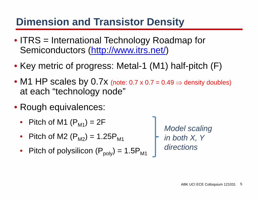
Dimension and Transistor Density• ITRS = International Technology Roadmap for
Semiconductors (http://www.itrs.net/)
• Key metric of progress: Metal-1 (M1) half-pitch (F)
• M1 HP scales by 0.7x (note: 0.7 x 0.7 = 0.49 density doubles)at each “technology node”
• Rough equivalences:• Pitch of M1 (PM1) = 2F
• Pitch of M2 (PM2) = 1.25PM1
• Pitch of polysilicon (Ppoly) = 1.5PM1
Model scaling in both X, Y directions
ABK UCI ECE Colloquium 121031 6
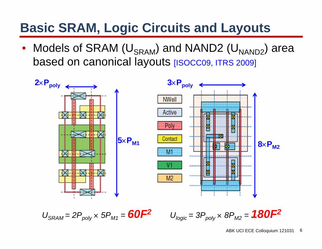
Basic SRAM, Logic Circuits and Layouts
5PM1
2Ppoly 3Ppoly
8PM2
• Models of SRAM (USRAM) and NAND2 (UNAND2) area based on canonical layouts [ISOCC09, ITRS 2009]
Ulogic = 3Ppoly 8PM2 = 180F2USRAM = 2Ppoly 5PM1 = 60F2

ABK UCI ECE Colloquium 121031 7
Historical Data for MPU Products
1.00E+07
1.00E+08
1.00E+09
1.00E+10
1.00E+11
1.00E+12
2005 2010 2015 2020 2025
MPU Logic TransistorDensity (xtors/cm^2)
SRAM transistordensity (xtors/cm^2)
1.00E+00
1.00E+01
1.00E+02
1.00E+03
1.00E+04
1.00E+05
1.00E+06
1.00E+07
1.00E+08
1.00E+09
1970 1975 1980 1986 1991 1997 2002 2008 2013
[Tx/cm2, ITRS 2007 MPU model] [Tx/cm2, Stanford CPUDB]
???
ABK UCI ECE Colloquium 121031 8
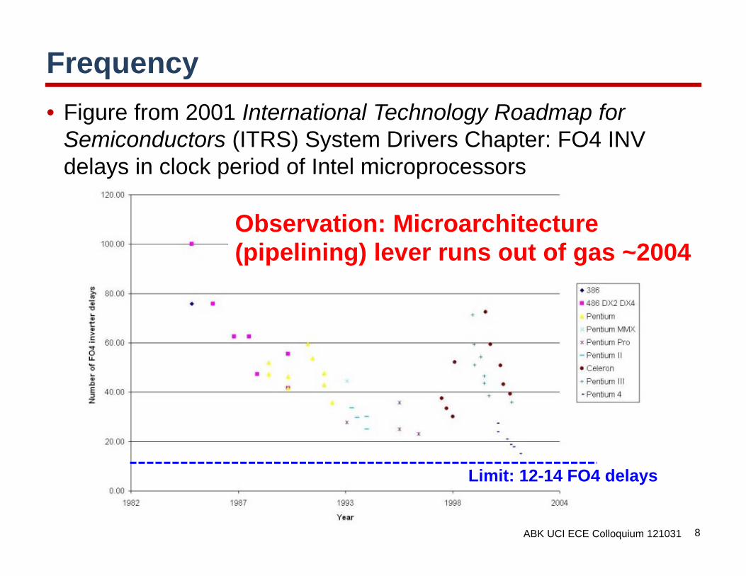
Frequency• Figure from 2001 International Technology Roadmap for
Semiconductors (ITRS) System Drivers Chapter: FO4 INV delays in clock period of Intel microprocessors
Limit: 12-14 FO4 delays
Observation: Microarchitecture (pipelining) lever runs out of gas ~2004
ABK UCI ECE Colloquium 121031 9
Power
0.00
0.01
0.02
0.03
0.04
0.05
0.06
2005 2010 2015 2020 2025
Logic Power static (density)(W/mm2)SRAM Power static (density)(W/mm2)
0.00
0.10
0.20
0.30
0.40
0.50
0.60
2005 2010 2015 2020 2025
Active cap density(nF/mm2)
[ITRS 2007]
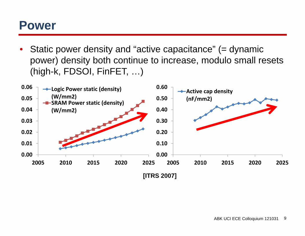
• Static power density and “active capacitance” (= dynamic power) density both continue to increase, modulo small resets (high-k, FDSOI, FinFET, …)

ABK UCI ECE Colloquium 121031 10
1
10
100
2001 2006 2011 2016 2021
Freq
uenc
y (G
Hz)
before 20012001 ITRS2007 ITRS2011 ITRS
ITRS MPU Frequency Roadmap
Device speed only
Platform power limit
Device scaling limit

ABK UCI ECE Colloquium 121031 11
1
10
100
2001 2006 2011 2016 2021
ITRS MPU Frequency Roadmap
Freq
uenc
y (G
Hz)
before 20012001 ITRS2007 ITRS2011 ITRS
[Danowitz et al., Stanford CPUDB]

ABK UCI ECE Colloquium 121031 12
Seeing the Future, With 20-20-20 Vision
TSMC 28nm 20nm: 30% higher speed, 25% less power
TSMC 40nm LP 28nm LP: 20% higher speed
UMC 40nm LP 28nm LP: 20% higher speed
Samsung 45nm 32nm: 30% higher speed, 30% less power

ABK UCI ECE Colloquium 121031 13
Seeing the Future, With 20-20-20 Vision
TSMC 28nm 20nm: 30% higher speed, 25% less power
TSMC 40nm LP 28nm LP: 20% higher speed
UMC 40nm LP 28nm LP: 20% higher speed
Samsung 45nm 32nm: 30% higher speed, 30% less power
Reality: In a new technology node, the best that designers can hope for is 20% less power, 20% more speed, and 20% better density
Corollary: 10% = half of a technology node that costs many $B
Challenge: How to extract value from new technology ?!?
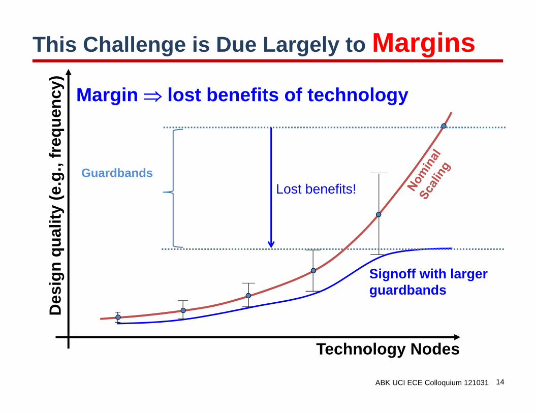
ABK UCI ECE Colloquium 121031 14
This Challenge is Due Largely to MarginsD
esig
n qu
ality
(e.g
., fr
eque
ncy)
Technology Nodes
Signoff with larger guardbands
Guardbands
Margin lost benefits of technology
Lost benefits!
ABK UCI ECE Colloquium 121031 15
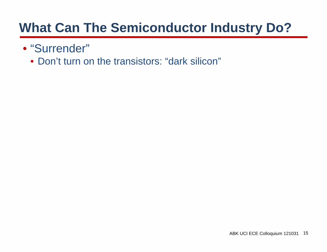
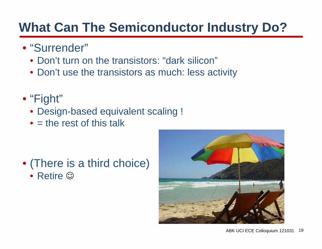
What Can The Semiconductor Industry Do?• “Surrender”
• Don’t turn on the transistors: “dark silicon”
ABK UCI ECE Colloquium 121031 16
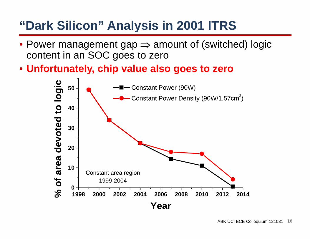
“Dark Silicon” Analysis in 2001 ITRS• Power management gap amount of (switched) logic
content in an SOC goes to zero• Unfortunately, chip value also goes to zero
1998 2000 2002 2004 2006 2008 2010 2012 20140
10
20
30
40
50
Constant area region1999-2004
Constant Power (90W)
Constant Power Density (90W/1.57cm2)
% o
f are
a de
vote
d to
logi
c
Year

ABK UCI ECE Colloquium 121031 17
What Can The Semiconductor Industry Do?• “Surrender”
• Don’t turn on the transistors: “dark silicon”• Don’t use the transistors as much: less activity

ABK UCI ECE Colloquium 121031 18
ITRS “Magical” Activity Factor Reduction
• To reduce dynamic power: Do less work• MPU power limit is maintained by assuming a “design-
based” reduction of switching activity (-5% per year)
0
50
100
150
200
250
300
350
400
450
2009
2010
2011
2012
2013
2014
2015
2016
2017
2018
2019
2020
2021
2022
2023
2024
2025
Power (W
)
Total Dynamic Power (W)NEW Total Dynamic Power (W)
With 5% per year reduction of switching activity
Power < 150W
ABK UCI ECE Colloquium 121031 19
What Can The Semiconductor Industry Do?• “Surrender”
• Don’t turn on the transistors: “dark silicon”• Don’t use the transistors as much: less activity
• “Fight” • Design-based equivalent scaling !• = the rest of this talk
• (There is a third choice)• Retire

ABK UCI ECE Colloquium 121031 20
“Design-Based Equivalent Scaling”
• Geometric scaling: Reduction of physical dimensions to improve density (cost per function), performance, reliability, etc.
• Examples: scaling of Tox , Lgate, gate pitch
Geometric Scaling[Bohr08]

ABK UCI ECE Colloquium 121031 21
• Equivalent scaling: Non-geometric enhancements of process, devices or materials to improve electrical performance
• Examples: High-K metal gate, FinFET devices
Equivalent Scaling
Geometric Scaling
[Mistry07]
“Design-Based Equivalent Scaling”
ABK UCI ECE Colloquium 121031 22
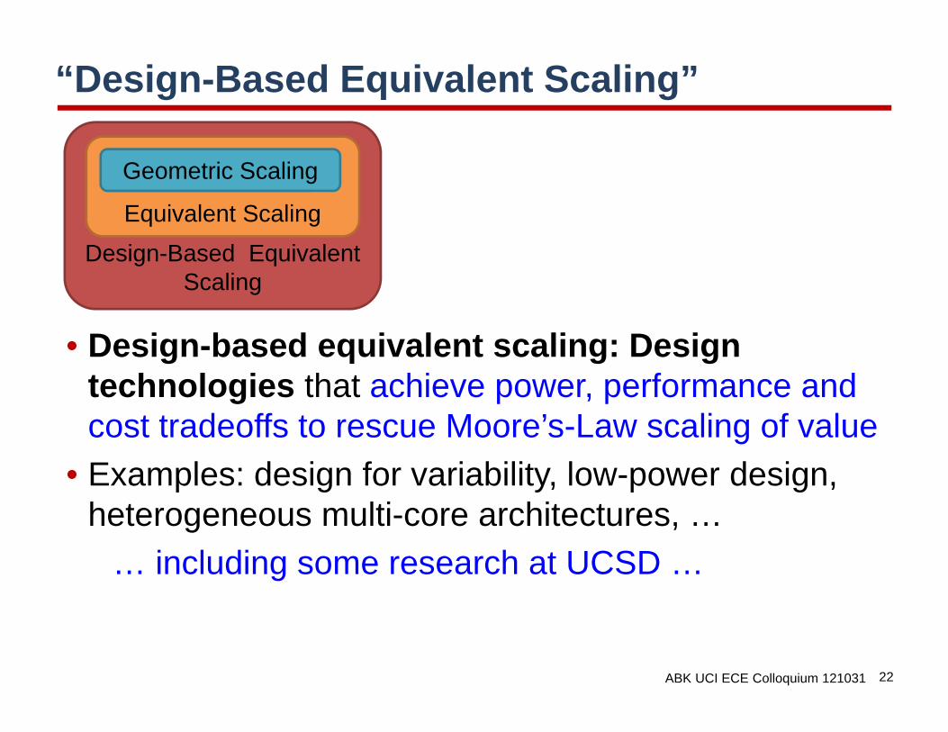
Design-Based Equivalent Scaling
• Design-based equivalent scaling: Design technologies that achieve power, performance and cost tradeoffs to rescue Moore’s-Law scaling of value
• Examples: design for variability, low-power design, heterogeneous multi-core architectures, …
… including some research at UCSD …
Equivalent Scaling
Geometric Scaling
“Design-Based Equivalent Scaling”
ABK UCI ECE Colloquium 121031 23
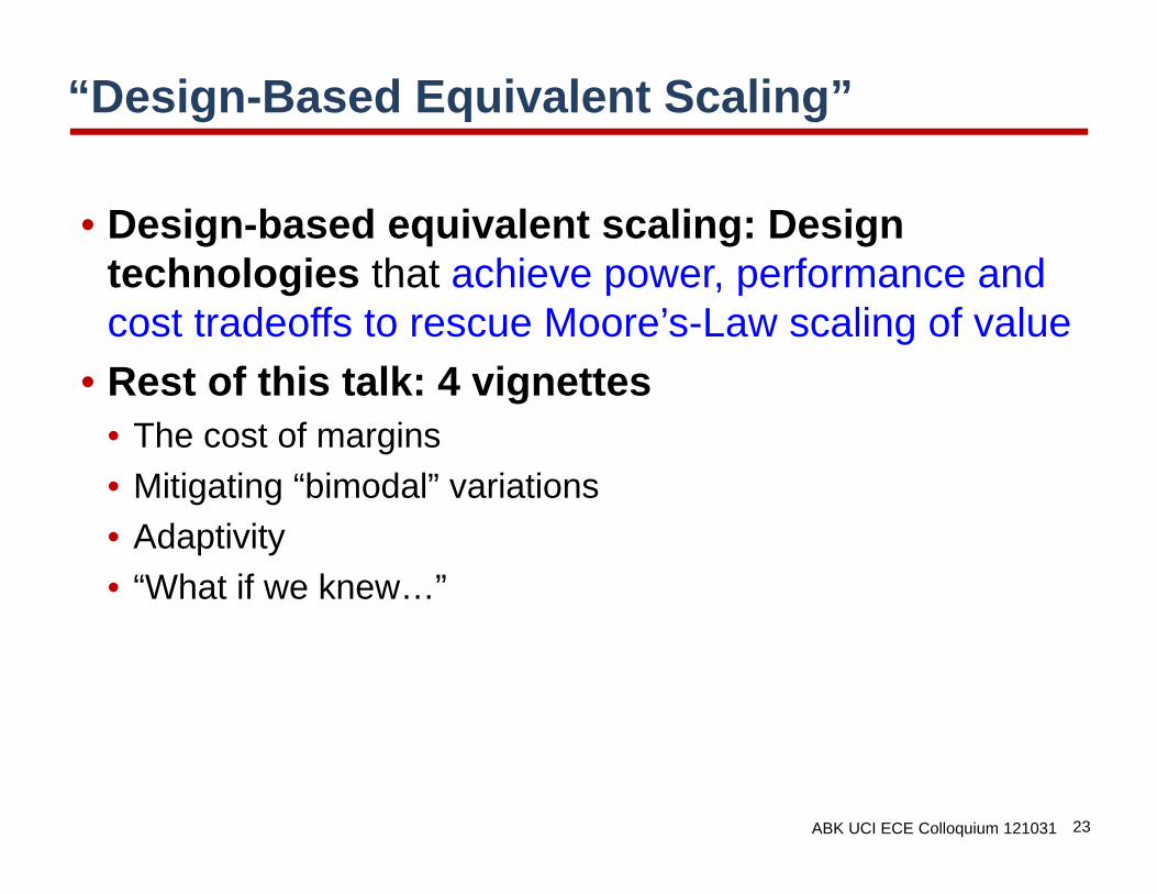
• Design-based equivalent scaling: Design technologies that achieve power, performance and cost tradeoffs to rescue Moore’s-Law scaling of value
• Rest of this talk: 4 vignettes• The cost of margins• Mitigating “bimodal” variations• Adaptivity• “What if we knew…”
“Design-Based Equivalent Scaling”

ABK UCI ECE Colloquium 121031 24
On the Cost of Margin (a.k.a. Guardband)
ABK UCI ECE Colloquium 121031 25
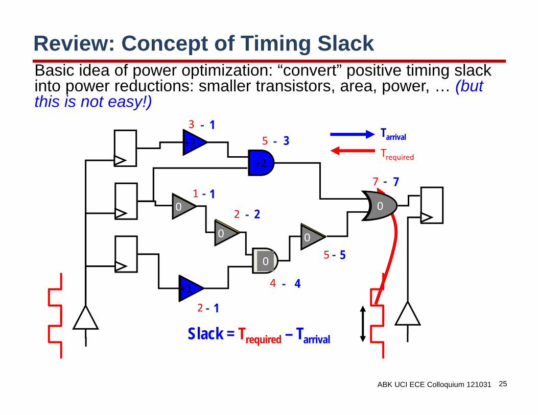
Review: Concept of Timing SlackBasic idea of power optimization: “convert” positive timing slack into power reductions: smaller transistors, area, power, … (but this is not easy!)
CLKSlack = Trequired – Tarrival
1
1
1
1
2
2
1
2
CLK
1
1
1
2
5
7
3
4
7
4
2
2
1
5
53
Tarrival
Trequired+2
+1
+2
0
0 0
0
0
-
-
-
-
-
-
-
-
ABK UCI ECE Colloquium 121031 26
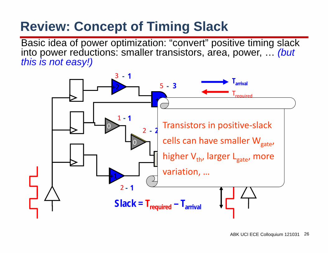
Review: Concept of Timing SlackBasic idea of power optimization: “convert” positive timing slack into power reductions: smaller transistors, area, power, … (but this is not easy!)
CLKSlack = Trequired – Tarrival
1
1
1
1
2
2
1
2
CLK
1
1
1
2
5
7
3
4
7
4
2
2
1
5
53
Tarrival
Trequired+2
+1
+2
0
0 0
0
0
-
-
-
-
-
-
-
-
Transistors in positive‐slack cells can have smaller Wgate, higher Vth, larger Lgate, more variation, …

ABK UCI ECE Colloquium 121031 27
Guardband for Variations• Guardband to cover uncertainties
• Traditional components of guardband
Defocus/Dose VariationMisalignment
TemperatureVariation
Reliability
Non-Rectangular ShapesLine-End Shortening
CrosstalkIR-drop
Imperfect regulatorsNon-Uniform CD
Erosion/Dishing in CMP
Electromigration
Hot-Carrier Injection
NBTI
Alpha-Particle
Line Edge Roughness
Mask CD Error
Wafer flatness Lens Aberration
Flare
ProcessVoltage Temp.FEOL BEOL
NMOS PMOS Cap. Res.
WORST Slow Slow Max. Min. Low(e.g. 0.9V)
High(e.g. 125C)
BEST Fast Fast Min. Max High(e.g. 1.1V)
Low(e.g. -40 C)
WCBC
Circuit delay
ABK UCI ECE Colloquium 121031 28
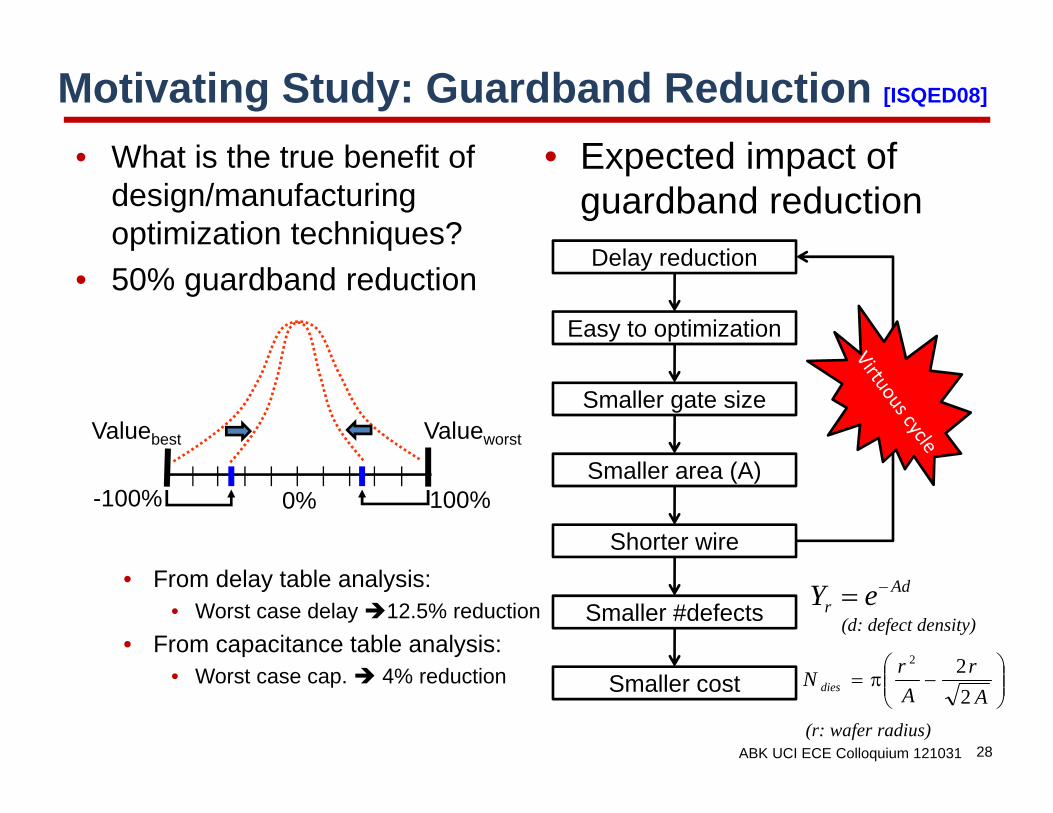
Motivating Study: Guardband Reduction [ISQED08]
• What is the true benefit of design/manufacturing optimization techniques?
• 50% guardband reduction
• From delay table analysis:• Worst case delay 12.5% reduction
• From capacitance table analysis:• Worst case cap. 4% reduction
• Expected impact of guardband reduction
Valuebest Valueworst
-100% 100%0%
Delay reduction
Easy to optimization
Smaller gate size
Smaller area (A)
Smaller #defects
Smaller cost
Shorter wire
Adr eY
Ar
ArN dies 2
22
(d: defect density)
(r: wafer radius)
ABK UCI ECE Colloquium 121031 29
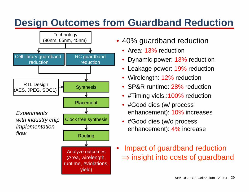
Design Outcomes from Guardband Reduction• 40% guardband reduction
• Area: 13% reduction• Dynamic power: 13% reduction• Leakage power: 19% reduction• Wirelength: 12% reduction• SP&R runtime: 28% reduction• #Timing viols.:100% reduction • #Good dies (w/ process
enhancement): 10% increases• #Good dies (w/o process
enhancement): 4% increase
• Impact of guardband reduction insight into costs of guardband
Cell library guardband reduction
Synthesis
RC guardbandreduction
Placement
Clock tree synthesis
Routing
Analyze outcomes(Area, wirelength,
runtime, #violations,yield)
RTL Design(AES, JPEG, SOC1)
Technology(90nm, 65nm, 45nm)
Experimentswith industry chipimplementationflow
ABK UCI ECE Colloquium 121031 30
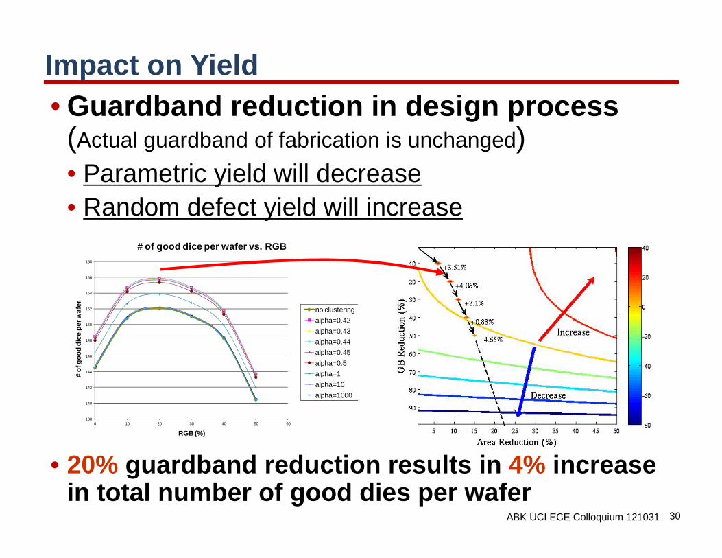
Impact on Yield• Guardband reduction in design process
(Actual guardband of fabrication is unchanged)• Parametric yield will decrease• Random defect yield will increase
• 20% guardband reduction results in 4% increase in total number of good dies per wafer
138
140
142
144
146
148
150
152
154
156
158
0 10 20 30 40 50 60
# of
goo
d di
ce p
er w
afer
RGB (%)
# of good dice per wafer vs. RGB
no clusteringalpha=0.42alpha=0.43alpha=0.44alpha=0.45alpha=0.5alpha=1alpha=10alpha=1000

ABK UCI ECE Colloquium 121031 31
On Taming Bimodality (Double-Patterning Lithography)
TSMC R&D VP Cliff Hou: “At 20nm the challenge is double patterning, …”
– October 24, 2012

ABK UCI ECE Colloquium 121031 32
CD Bimodality in Double-Patterning Litho
C12-type cell C21-type cell
Gates from CD group1Gates from CD group2
• Two patterning steps Two different CDs
• Two different colorings Two different timings
Green linesfrom 1st patterning
Blue linesfrom 2nd patterning
C12: Odd polys in BLUE, Even polys in GREEN
C21: Odd polys in GREEN, Even polys in BLUE
CD = “Critical Dimension”

ABK UCI ECE Colloquium 121031 33
0.0E+00
5.0E-12
1.0E-11
1.5E-11
2.0E-11
2.5E-11
3.0E-11
1 nm 2 nm 3 nm 4 nm 5 nm 6 nm
Del
ay (s
)
CD Mean Difference
Best case: Large CD groupWorst case: Large CD groupBest case: Small CD groupWorst case: Small CD groupBest case: Pooled CDWorst case: Pooled CD
Bimodality Impact on Guardband [SPIE08, ASPDAC09]
• Comparison of design guardband (Min-Max delay)• Unimodal representation is too pessimistic
CD mean difference
Large CD group
Small CD group

ABK UCI ECE Colloquium 121031 34
Impact of Bimodality on Path Delay• Bimodality can help reduce path delay variation
• Reduction of covariance when alternately colored
C12 C12 C12 C12
C12 C21 C12 C21
++
++
+‐
+‐
+4
0
Variation () is accumulated
Variation () is compensated0
5
10
15
20
25
0 1 2 3 4 5 6CD Mean Difference (nm)
Uniform
Alternate
Sigm
a / M
ean
(%)
SPICE Simulation Results

ABK UCI ECE Colloquium 121031 35
• Different coloring sequences in a clock network Clock skew
• Same color on all clock buffers is better!
Impact of Bimodality on Clock Skew
Case Source to Sink A Source to Sink B1 C12+C12+C12+…+C12 C12+C12+C12+…+C122 C12+C12+C12+…+C12 C21+C21+C21+…+C21
0.00E+00
1.00E-11
2.00E-11
3.00E-11
4.00E-11
5.00E-11
6.00E-11
0nm 1nm 2nm 3nm 4nm 5nm 6nm
CD mean difference
Case2
Case1
Clo
ck s
kew
(s)

ABK UCI ECE Colloquium 121031 36
Bimodal CD Distribution: 3 Key Facts
1. Design requires bimodal-aware timing models
• Unimodal representation is too pessimistic
2. Data paths benefit from alternate (mixed) coloring
• Exploit existence of two uncorrelated CD populations
• Minimize correlated variations in a given path
3. Clock paths benefit from uniform coloring
• Correlated variation between launch and capture paths
minimizes bimodality-induced clock skew Principle: Design can exploit both correlated, uncorrelated variations

ABK UCI ECE Colloquium 121031 37
RTL‐to‐GDS
DPL Mask Coloring
Bimodal‐AwareTiming Analysis
Maximization ofAlternate Coloring
(Datapaths)
Optimization 1
Alternate coloringusing integer‐linear programming
Placement Perturbationfor Color Conflict Removal(Clock and Data paths)
Optimization 2
Coloring conflict > Minimum resolution
Placement perturbation usingdynamic programming
DPL Layout-to-Mask Flow
ABK UCI ECE Colloquium 121031 38
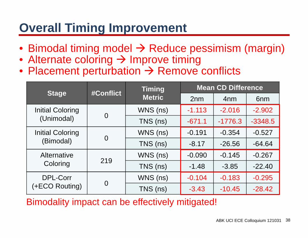
Overall Timing Improvement• Bimodal timing model Reduce pessimism (margin)• Alternate coloring Improve timing• Placement perturbation Remove conflicts
Stage #Conflict TimingMetric
Mean CD Difference2nm 4nm 6nm
Initial Coloring(Unimodal) 0
WNS (ns) -1.113 -2.016 -2.902TNS (ns) -671.1 -1776.3 -3348.5
Initial Coloring(Bimodal) 0
WNS (ns) -0.191 -0.354 -0.527TNS (ns) -8.17 -26.56 -64.64
AlternativeColoring 219
WNS (ns) -0.090 -0.145 -0.267TNS (ns) -1.48 -3.85 -22.40
DPL-Corr(+ECO Routing) 0
WNS (ns) -0.104 -0.183 -0.295TNS (ns) -3.43 -10.45 -28.42
Bimodality impact can be effectively mitigated!
ABK UCI ECE Colloquium 121031 39
On Adaptivity
ABK UCI ECE Colloquium 121031 40
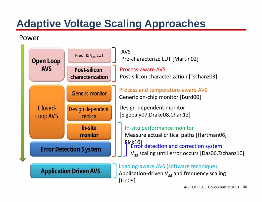
Adaptive Voltage Scaling Approaches
Open Loop AVS
Closed-Loop AVS
Error Detection System
Freq. & Vdd LUT
Post-silicon characterization
Generic monitor
Power
Design dependent replica
In-situmonitor
AVS Pre‐characterize LUT [Martin02]
Process‐aware AVSPost‐silicon characterization [Tschanz03]
Process and temperature‐aware AVS Generic on‐chip monitor [Burd00]
Design‐dependent monitor [Elgebaly07,Drake08,Chan12]
In‐situ performance monitor Measure actual critical paths [Hartman06, Fick10]Error detection and correction system Vdd scaling until error occurs [Das06,Tschanz10]
Application Driven AVSLoading‐aware AVS (software technique)Application‐driven Vdd and frequency scaling [Lin09]
ABK UCI ECE Colloquium 121031 41
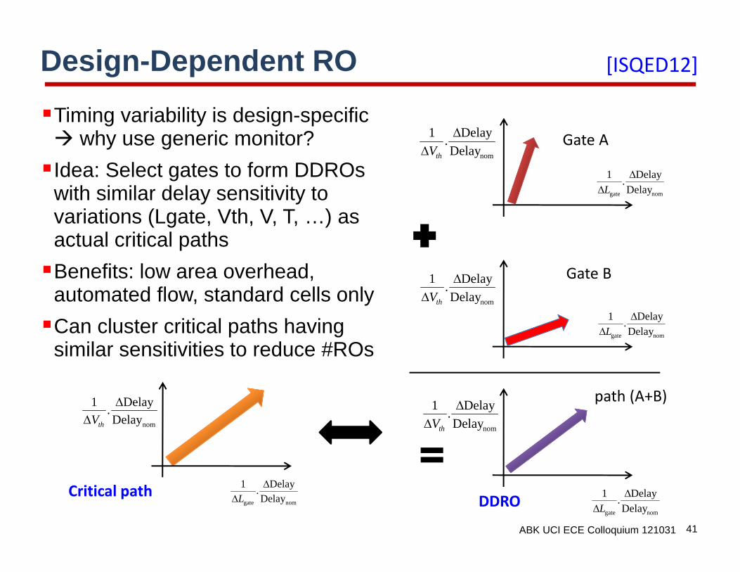
Design-Dependent ROTiming variability is design-specific why use generic monitor?Idea: Select gates to form DDROs
with similar delay sensitivity to variations (Lgate, Vth, V, T, …) as actual critical pathsBenefits: low area overhead,
automated flow, standard cells onlyCan cluster critical paths having
similar sensitivities to reduce #ROs
Critical path
nomDelayDelay.1
thV
nomgate DelayDelay.1
L
Gate A
Gate B
DDRO
path (A+B)
nomDelayDelay.1
thV
nomgate DelayDelay.1
L
nomDelayDelay.1
thV
nomDelayDelay.1
thV
nomgate DelayDelay.1
L
nomgate DelayDelay.1
L
[ISQED12]
ABK UCI ECE Colloquium 121031 42
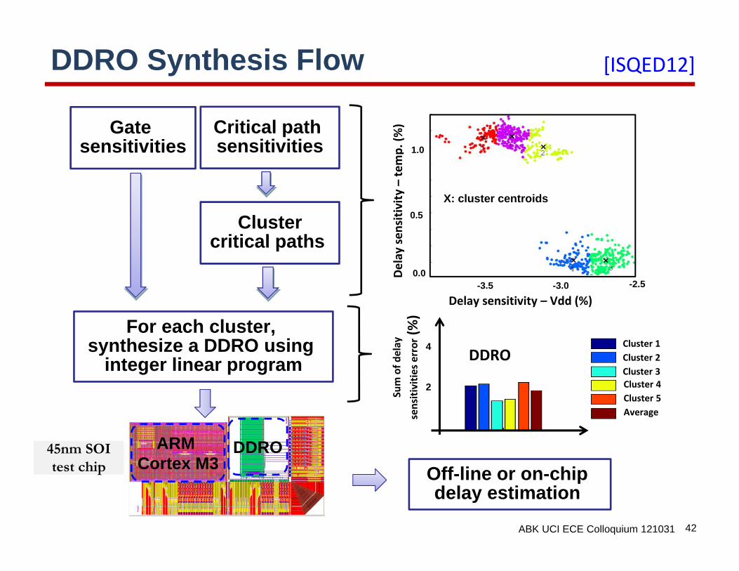
DDRO Synthesis Flow
Critical path sensitivities
For each cluster, synthesize a DDRO using
integer linear program
Gate sensitivities
Clustercritical paths
ARM Cortex M3
DDRO45nm SOItest chip
X: cluster centroids
Off-line or on-chip delay estimation
Cluster 1Cluster 2Cluster 3Cluster 4Cluster 5Average
DDRODDRO
Sum of d
elay
sensitivitie
s error(%
)
2
4
Delay sen
sitiv
ity –temp. (%
)
0.5
0.0
1.0
Delay sensitivity – Vdd (%)-3.5 -3.0 -2.5
X: cluster centroids
[ISQED12]

ABK UCI ECE Colloquium 121031 43
Design-Dependent RO vs. Generic RO
DDRO
1.0 1.20.9 1.1
1.2
1.0
1.1
0.9
hvt+rvt Inv RO
1.00.9 1.1
1.2
1.0
1.1
0.91.2
Estimation error= ‐0.5 % ~ 3.7 %
Estimation error = ‐1.7 % ~ 5.1 %
Actual delay (ns) Actual delay (ns)
Estim
ated
delay (n
s)
Estim
ated
delay (n
s)
0
0.01
0.02
0.03
0.04
0.05
0.06
0.07
0.08
DDRO Critical pathreplica
hvt+rvt INV RO
Std. deviatio
n of f m
ax
Std. Deviation of Fmax
Copy1
Copy2
Copy3
00.10.20.30.40.50.60.70.80.91
DDRO Critical path replicahvt+rvt INV RO
Correlation Co
eficient
Fmax Correlation Coefficient
Copy1
Copy2
Copy3
• 45nm test chip measurementEach monitor have 3 copies per chip, 19 chips (no wafer split)
• SPICE Monte Carlo Simulation 30 samples
[ISQED12]
ABK UCI ECE Colloquium 121031 44
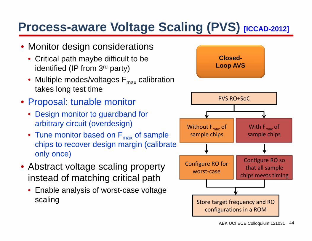
Process-aware Voltage Scaling (PVS) [ICCAD-2012]
• Monitor design considerations• Critical path maybe difficult to be
identified (IP from 3rd party)• Multiple modes/voltages Fmax calibration
takes long test time
• Proposal: tunable monitor• Design monitor to guardband for
arbitrary circuit (overdesign)• Tune monitor based on Fmax of sample
chips to recover design margin (calibrate only once)
• Abstract voltage scaling property instead of matching critical path• Enable analysis of worst-case voltage
scaling
PVS RO+SoC
Without Fmax of sample chips
With Fmax of sample chips
Store target frequency and RO configurations in a ROM
Configure RO for worst‐case
Configure RO so that all sample
chips meets timing
Closed-Loop AVS

ABK UCI ECE Colloquium 121031 45
Voltage Scaling Properties• Vmin= Minimum Vdd to meet timing constraints
= process distance/scaling rate• Process distance: process-induced frequency shift
relative to target frequency• Scaling rate: frequency shift for a unit voltage difference
V
FF
TT
SS
k
targetf
)(kVmin_path nomV VVnom
Process distance
Freq.
Scaling rate =Vf
ABK UCI ECE Colloquium 121031 46
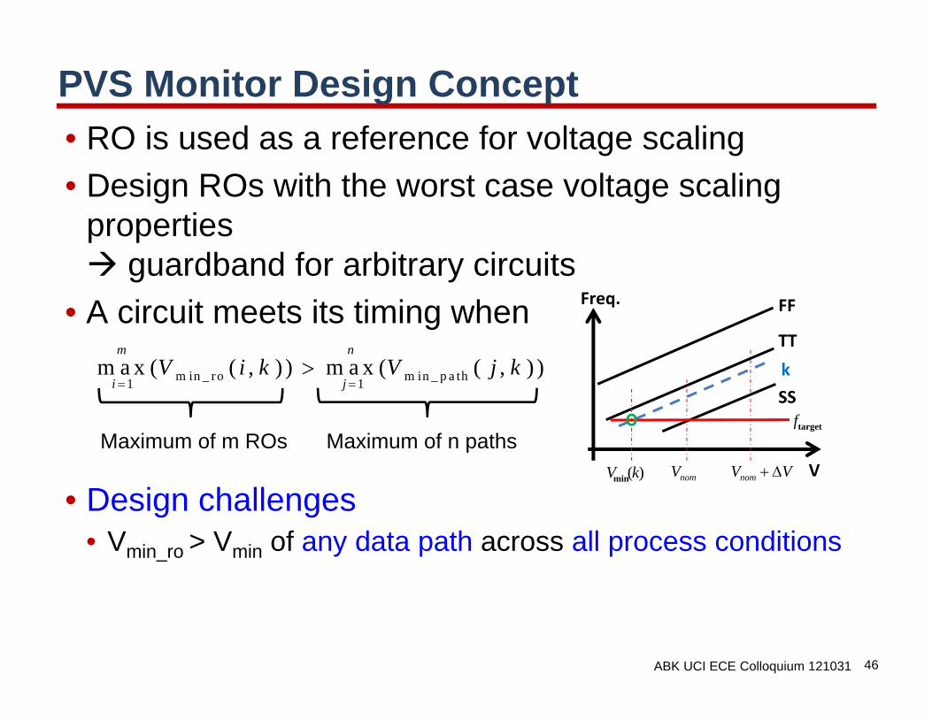
PVS Monitor Design Concept• RO is used as a reference for voltage scaling• Design ROs with the worst case voltage scaling
properties guardband for arbitrary circuits
• A circuit meets its timing when
• Design challenges• Vmin_ro > Vmin of any data path across all process conditions
V
FF
TT
SSk
targetf
)(kVmin nomV VVnom
Freq.
m in _ ro m in _ p a th1 1m a x ( ( , ) ) m a x ( ( , ) )
m n
i jV i k V j k
Maximum of m ROs Maximum of n paths

ABK UCI ECE Colloquium 121031 47
0.500
0.600
0.700
0.800
0.900
1.000
1.100
INVX0 NAND2X0 NAND3X0 NAND4X0 NOR2X0 NOR3X0 NOR4X0
Vmin(V)
Cell type
SS TT FF SF FS
Vmin Analysis• Key observation: Vmin is bounded by NMOS or PMOS
dominated cells (e.g., NOR3 at FS corner)Use NAND, NOR type ROs

ABK UCI ECE Colloquium 121031 48
Design RO with Tunable Vmin• Identified two circuit knobs to tune Vmin
• Series resistance• Cell types (INV, NAND, NOR)
• Example circuit strategy• Allow tuning of series resistance of each stage to high or low• Different cell types cover different process corners
1 bit 1 bit 1 bit
Control pins
High resistance
Low resistance

ABK UCI ECE Colloquium 121031 49
PVS Experiment Result
• Default setting: low resistance in all stages Vmin_est – Vmin_chip = 13mV on average (guardband for worst-case)
• With Fmax information per die, can tune RO configuration to drive Vmin_est – Vmin_chip 0
• Better on-chip sensing and adaptation more reduction of runtime power overheads (Vdd)
More aggressive scaling
Min margin
65nm, OpenSPARC T1 moduleMonte Carlo SPICE simulation

ABK UCI ECE Colloquium 121031 50
On “What if We Knew …”

ABK UCI ECE Colloquium 121031 51
What If We Knew…(switching activity from workload)
Error‐Tolerant Design
CPU, heal thyself ...
Errors are detected and corrected with redundancy technique
Problem: • Many paths have near‐critical slack → wall of (critical) slack
• Scaling beyond the critical operating point causes massive errors that cannot be corrected
Frequently‐exercised paths: upsize cellsRarely‐exercised paths: downsize cells
Reshape slack distribution for gracefully increasing error rate
Scale voltage further
ABK UCI ECE Colloquium 121031 52
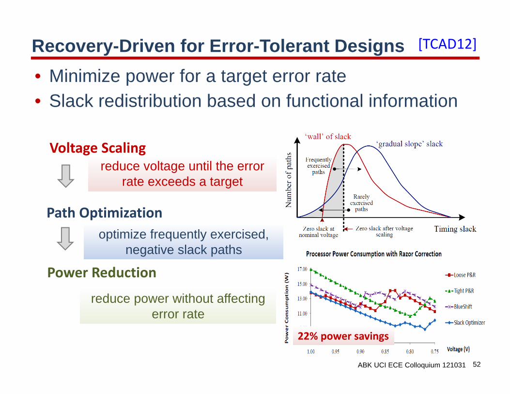
Recovery-Driven for Error-Tolerant Designs• Minimize power for a target error rate• Slack redistribution based on functional information
[TCAD12]
Power Reduction
reduce voltage until the error rate exceeds a target
optimize frequently exercised, negative slack paths
reduce power without affecting error rate
Voltage Scaling
Path Optimization
22% power savings

ABK UCI ECE Colloquium 121031 53
What If We Knew … (scenarios, duty cycles) Dynamic Voltage Freq. Scaling
• DVFS allows adaptation to workloads & operating conditions
• Multi-Mode (or DVFS) design operates at multiple power/performance points with different lifetimes
1.0V, 1GHz(e.g., talk mode)
0.7V, 100MHz(e.g., standby mode)
• Conventional EDA tool: require constraints (freq., voltage) before implementation (which constraints will provide minimum energy?)
• Replication: Create replicas that target each performance mode(Replication incurs a large area overhead)Use scenario/duty cycle information for multi-mode optimization [TCAD12]
ABK UCI ECE Colloquium 121031 54
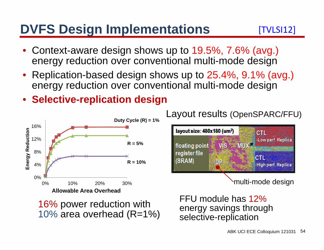
DVFS Design Implementations• Context-aware design shows up to 19.5%, 7.6% (avg.)
energy reduction over conventional multi-mode design• Replication-based design shows up to 25.4%, 9.1% (avg.)
energy reduction over conventional multi-mode design• Selective-replication design
FFU module has 12%energy savings through selective-replication
multi-mode design
Layout results (OpenSPARC/FFU)
16% power reduction with 10% area overhead (R=1%)
0%
4%
8%
12%
16%
0% 10% 20% 30%
Ener
gy R
educ
tion
Allowable Area Overhead
Duty Cycle (R) = 1%
R = 5%
R = 10%
[TVLSI12]

ABK UCI ECE Colloquium 121031 55
What If We Knew … (accuracy requirements)
Problem: • Accuracy requirement can change during runtime benefits of approximation could be reduced
Adapt to changing requirements with runtime accuracy configuration
[DAC 2012]“accuracy‐configurableapproximate adder”
Approximate DesignWhat is the square root of 10 ?
“a little more than three”
“3.162278...”Approximation could be faster and more powerful
higher accuracylower power consumption

ABK UCI ECE Colloquium 121031 56
Accuracy-Configurable Adder
• Power reduction when accuracy requirement varying
0
0.2
0.4
0.6
0.8
1
Normalize
d po
wer
consum
ption mode‐4
mode‐3
mode‐2
mode‐1
0.98 Accuracy 1.00
Average 30% power savings vs. no accuracy configuration
referencereferenceresultAvgAccuracy ||1.
Config. Accuracy Power reduction
1.000 ‐11.5%
0.998 12.4%
0.991 31.0%
0.983 51.6%
[DAC12]
• Accuracy configuration with pipelined adder

ABK UCI ECE Colloquium 121031 57
What If We Knew … (Lifetime (MTTF) Reqts)
AF (α)
Jrms
Temp
Wire width
MTTF
Driver size
A B Inverse relation; if A increases then B decreases
A BDirect relation; if A increases then B increases
Supply voltage
Timing slack
|Vthp |
Wire spacing
TDDB
TDDB
EM
EM
Freq.|Vthn |
Slew rate
Load/fanout
Gate length
Junction resistance
EM, TDDB, NBTI, HCI
HCINBTI
HCIHCI
HCI
HCI
HCI
HCI
NBTI
Tunable at design or runtime
Tunable at design
general
general
general
generalgeneral
general
general
general
generalgeneral
general
general
general
general
general
general
general
HCI
HCI
NBTI

ABK UCI ECE Colloquium 121031 58
Example: Electromigration MTTF vs. Fmax
• Fmax increases with relaxing MTTFrequire• Up to +60% of Fmax for -30% of MTTFrequire
• Fmax improvement is determined by • Mix of cell sizes• Length and timing constraints of critical paths
0%
20%
40%
60%
80%
100%
10 9 8 7 6 5 4 3 2 1
% in
crea
se o
f Fm
ax DMA AES JPEG
-30% of MTTFrequire= +60% of Fmax
• 65nm technology• Fixed area
ABK UCI ECE Colloquium 121031 59
Conclusions• A new technology node costs billions of dollars in
technology development and hundreds of millions of dollars in design enablement
• Leading-edge companies accept these costs to gain “20%” advantages
• Design-based equivalent scaling offers entire technology nodes of improvements that are essential to the continuation of “Moore’s Law”
• Recurring theme: “What if we knew…”• Bridges between design and manufacturing• Bridges between system design and IC implementation

ABK UCI ECE Colloquium 121031 60
THANK YOU


