March 17, 2011 • Santa Clara, California Design for reliability of BEoL and 3‐D TSV structures – A joint effort of FEA and innovative experimental techniques Jürgen Auersperg 1 , D. Vogel 1 , M.U. Lehr 3 , M. Grillberger 3 , J. Oswald 3 , S. Rzepka 1 , B. Michel 1,2 1 Fraunhofer Institute for Electronic Nano Systems ENAS, Germany 2 l hf f l bl d 2 Micro Materials Center at Fraunhofer Institute for Reliability and Microintegration IZM, Germany 4 GLOBALFOUNDRIES Dresden Module One LLC & Co. KG, Dresden, Germany Micro Materials Center Chemnitz Heads: Prof. B. Michel and Dr. Sven Rzepka
Transcript
March 17, 2011 • Santa Clara, California
Design for reliability of BEoL and 3‐D TSV structures – A joint effort of FEA and innovative experimental techniques
Jürgen Auersperg1, D. Vogel1, M.U. Lehr3, M. Grillberger3, J. Oswald3, S. Rzepka1, B. Michel1,2
1 Fraunhofer Institute for Electronic Nano Systems ENAS, Germany2 l h f f l b l d2Micro Materials Center at Fraunhofer Institute for Reliability and Microintegration IZM, Germany
4GLOBALFOUNDRIES Dresden Module One LLC & Co. KG, Dresden, Germany
Micro Materials Center ChemnitzHeads: Prof. B. Michel and
Dr. Sven Rzepka
Outline
Motivation
Multi‐level FE modeling of CPI
Multi‐failure evaluation for Near‐Chip‐Edge and Near‐Bump Cracks in BEoL
Role of Initial Stresses
TSV –damage and delamination investigation
Required experimentsRequired experiments
Summary and Outlook
Jürgen Auersperg D Vogel M U LehrJürgen Auersperg, D. Vogel, M.U. Lehr, M. Grillberger, J. Oswald, S. Rzepka, B. Michel Micro Materials Center Chemnitz
Heads: Prof. B. Michel andDr. Sven Rzepka
Task – Heterogeneous Integration ‐ Packaging
Bridging the gap between chip and application
Bump side
Transistor side
<10 µm
Jürgen Auersperg D Vogel M U Lehr
nm, µmNanostructures
cm, mApplications
Jürgen Auersperg, D. Vogel, M.U. Lehr, M. Grillberger, J. Oswald, S. Rzepka, B. Michel Micro Materials Center Chemnitz
Heads: Prof. B. Michel andDr. Sven Rzepka
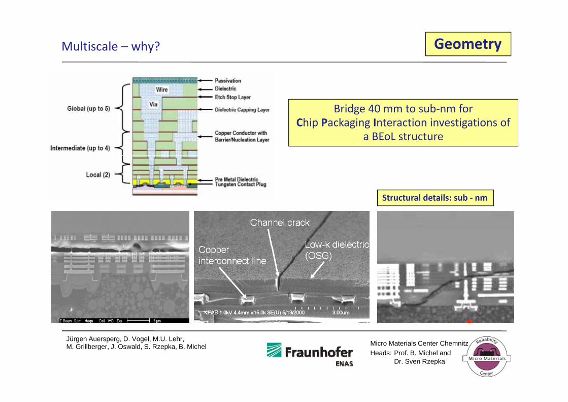
Multiscale – why? Geometry
Packaged microprocessor(eight symmetric model
Packaged microprocessor(10 – 40 mm size) PI layerNi layerBEoL stack region
HMT solderUnderfill
Bump side
HMT solder
Soldermask
LJT solder
gap<10
BEoL‐stack(5 – 10 µm size)
Jürgen Auersperg D Vogel M U Lehr
Boardpad
LJT solder
Transistor side
µm
Solder interconnect with BEoL‐stack(50 – 80 µm size)
Feature sizes: some nm!
Jürgen Auersperg, D. Vogel, M.U. Lehr, M. Grillberger, J. Oswald, S. Rzepka, B. Michel Micro Materials Center Chemnitz
Heads: Prof. B. Michel andDr. Sven Rzepka
Multiscale – why? Geometry
Bridge 40 mm to sub‐nm forBridge 40 mm to sub nm for Chip Packaging Interaction investigations of
a BEoL structure
Structural details: sub ‐ nm
Jürgen Auersperg D Vogel M U LehrJürgen Auersperg, D. Vogel, M.U. Lehr, M. Grillberger, J. Oswald, S. Rzepka, B. Michel Micro Materials Center Chemnitz
Heads: Prof. B. Michel andDr. Sven Rzepka
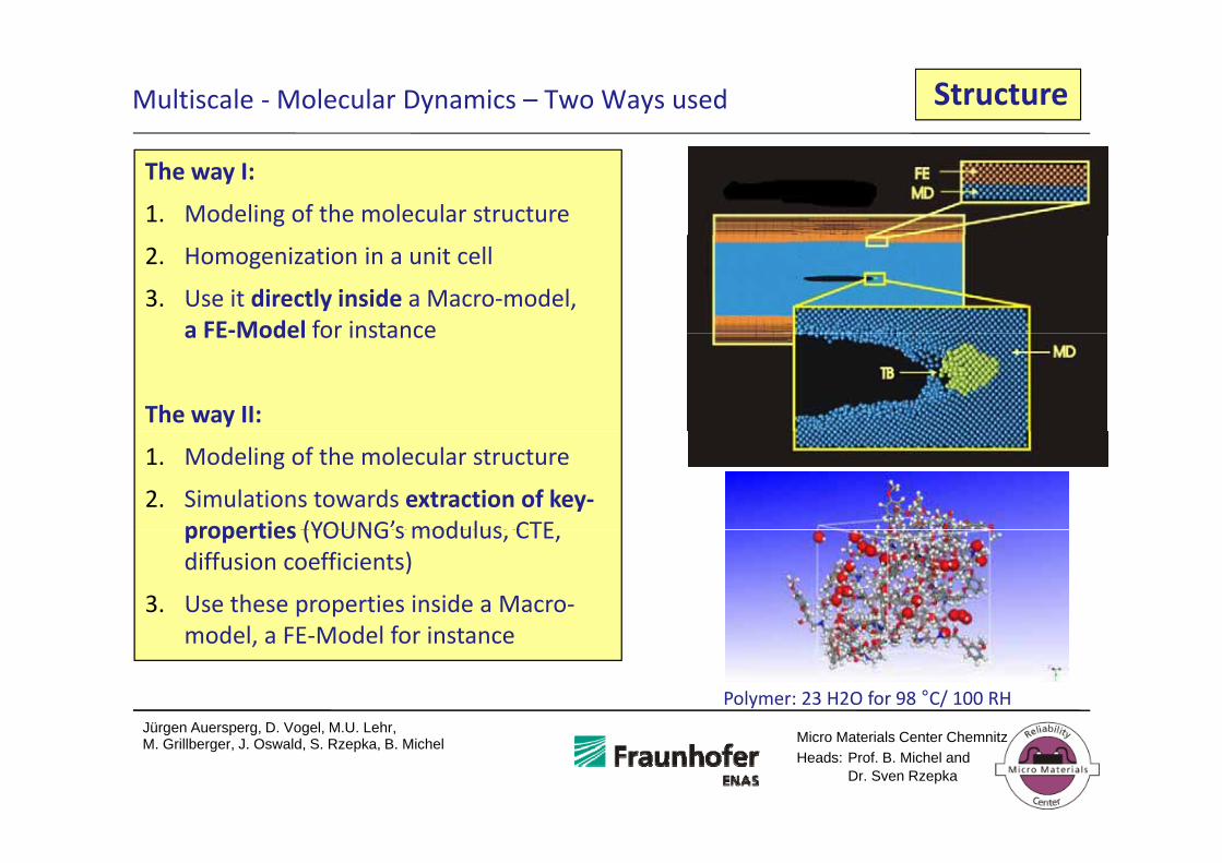
Multiscale – why? Structure
Nano lawn for interconnect formation
Can these materials longer be modeled as homogeneous
Jürgen Auersperg, D. Vogel, M.U. Lehr, M. Grillberger, J. Oswald, S. Rzepka, B. Michel Micro Materials Center Chemnitz
Heads: Prof. B. Michel andDr. Sven Rzepka
Multiscale ‐Molecular Dynamics – Two Ways used Structure
The way I:
1. Modeling of the molecular structure
2. Homogenization in a unit cell
3. Use it directly inside a Macro‐model,a FE‐Model for instancea FE Model for instance
The way II:
Finite Element Region
1. Modeling of the molecular structure
2. Simulations towards extraction of key‐properties (YOUNG’s modulus CTEFinite Element Region
Crack Tip Molecular Dynamics Region
properties (YOUNG s modulus, CTE, diffusion coefficients)
3. Use these properties inside a Macro‐d l FE M d l f i
Jürgen Auersperg D Vogel M U Lehr
model, a FE‐Model for instance
Polymer: 23 H2O for 98 °C/ 100 RHJürgen Auersperg, D. Vogel, M.U. Lehr, M. Grillberger, J. Oswald, S. Rzepka, B. Michel Micro Materials Center Chemnitz
Heads: Prof. B. Michel andDr. Sven Rzepka
M i i
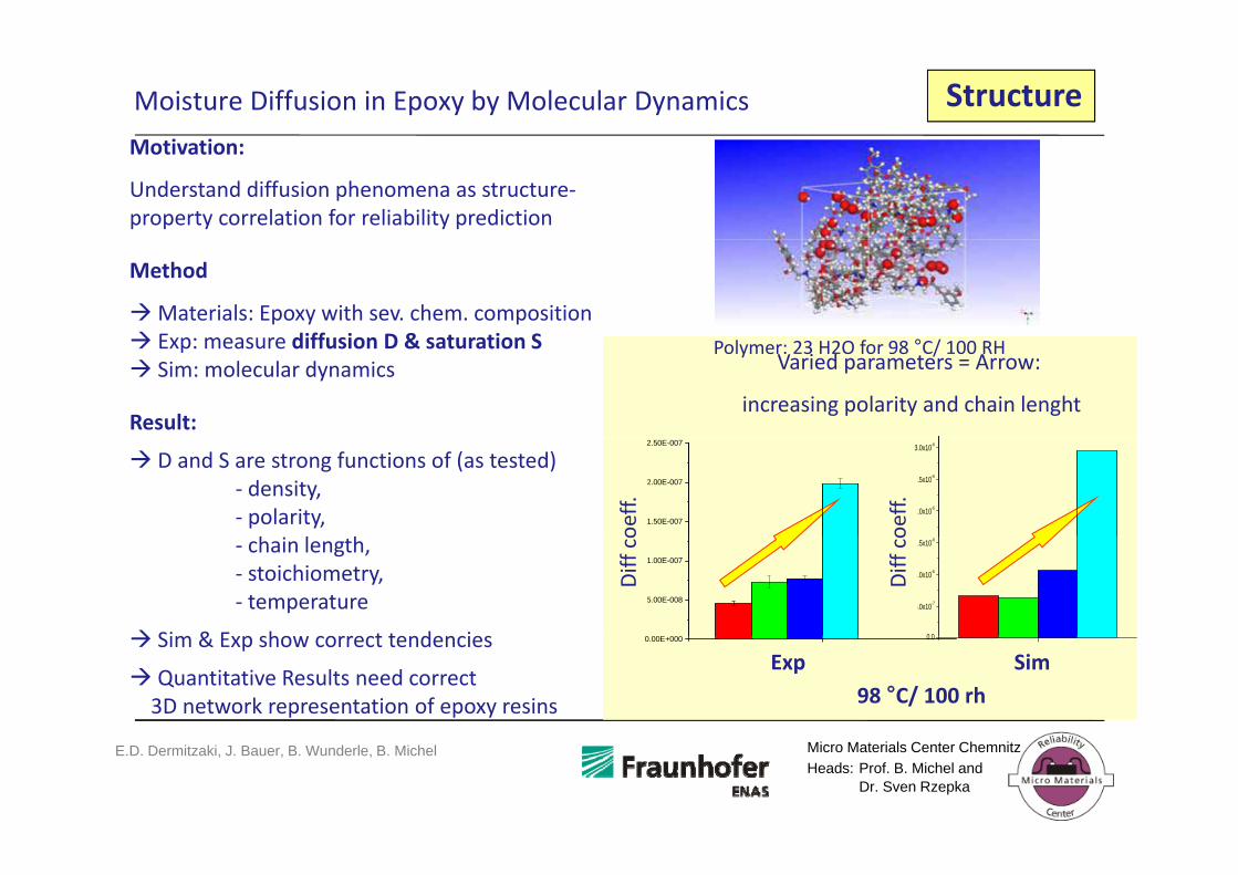
Moisture Diffusion in Epoxy by Molecular Dynamics StructureMotivation:
Understand diffusion phenomena as structure‐property correlation for reliability prediction
Method
Materials: Epoxy with sev. chem. composition Exp: measure diffusion D & saturation S
Varied parameters = Arrow:
increasing polarity and chain lenght
Exp: measure diffusion D & saturation S Sim: molecular dynamics
Result:
Polymer: 23 H2O for 98 °C/ 100 RH
2.0x10⁻⁶
2.5x10⁻⁶
3.0x10⁻⁶
2/s)1.50E-007
2.00E-007
2.50E-007
m^2
/s)
oeff.
oeff.
D and S are strong functions of (as tested) ‐ density, ‐ polarity, h l h
0 0
5.0x10⁻⁷
1.0x10⁻⁶
1.5x10⁻⁶
D (c
m^
0 00E 000
5.00E-008
1.00E-007
D (c
mDiff co
Diff co
‐ chain length, ‐ stoichiometry, ‐ temperature
Sim & Exp show correct tendencies
Jürgen Auersperg D Vogel M U Lehr
Molecular Dynamics 98°C/100RH0.0
Experiment:98°C/100RH0.00E+000
SimExp98 °C/ 100 rh
Sim & Exp show correct tendencies
Quantitative Results need correct 3D network representation of epoxy resins
Jürgen Auersperg, D. Vogel, M.U. Lehr, M. Grillberger, J. Oswald, S. Rzepka, B. Michel Micro Materials Center Chemnitz
Heads: Prof. B. Michel andDr. Sven Rzepka
E.D. Dermitzaki, J. Bauer, B. Wunderle, B. Michel
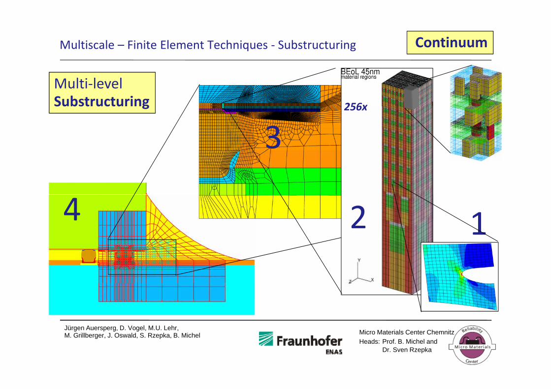
Multiscale – Finite Element Techniques ‐ Substructuring Continuum
Jürgen Auersperg D Vogel M U LehrJürgen Auersperg, D. Vogel, M.U. Lehr, M. Grillberger, J. Oswald, S. Rzepka, B. Michel Micro Materials Center Chemnitz
Heads: Prof. B. Michel andDr. Sven Rzepka
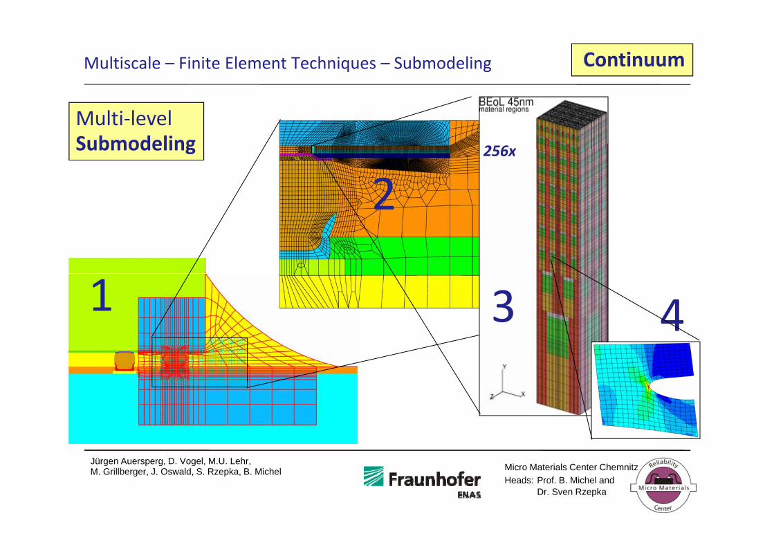
Multiscale – Finite Element Techniques – Submodeling Continuum
256x
Multi‐level Submodeling 256x
2Submodeling
31 4
Jürgen Auersperg D Vogel M U LehrJürgen Auersperg, D. Vogel, M.U. Lehr, M. Grillberger, J. Oswald, S. Rzepka, B. Michel Micro Materials Center Chemnitz
Heads: Prof. B. Michel andDr. Sven Rzepka
Multi‐failure Evaluationf
Micro Materials Center ChemnitzHeads: Prof. B. Michel and
Dr. Sven Rzepka
2nd Failure‐Mode – Risk for Die‐Cracking, Cracking of Substrates, …
Stress field with stress singularity
r1Smooth bending w/o singularities in stresses/strains
Stress field with well known stress singularity 1stresses/strains singularity r1
Cl i l t th h th G li d t i t it F t h i
Well known angle from anisotropic etching, for instance
Fracture mechanics: K‐factor (SIF), J‐integral, energy release rate (ERR) …
Jürgen Auersperg, D. Vogel, M.U. Lehr, M. Grillberger, J. Oswald, S. Rzepka, B. Michel Micro Materials Center Chemnitz
Heads: Prof. B. Michel andDr. Sven Rzepka
3rd Failure‐Mode – Delamination at Materials Interfaces
20µm
rrKi iyyxx 2/)( 0 Hutchinson et al.
1992
xyyy forarandforar
exp2
2exp2 *
00
Jürgen Auersperg D Vogel M U Lehr
Mixed Mode Situation 2
Jürgen Auersperg, D. Vogel, M.U. Lehr, M. Grillberger, J. Oswald, S. Rzepka, B. Michel Micro Materials Center Chemnitz
Heads: Prof. B. Michel andDr. Sven Rzepka
Cohesive Zone Modeling – Drawbacks and Challenges CZM
DCB specimen with crack propagation under continuous displacement controlled opening ! CZM‐Models have to handle and
deliver damage parameters (damage progress per(damage progress per cycle/time)
CZM with damage options
Jürgen Auersperg D Vogel M U Lehr
Subjects of current research!
Jürgen Auersperg, D. Vogel, M.U. Lehr, M. Grillberger, J. Oswald, S. Rzepka, B. Michel Micro Materials Center Chemnitz
Heads: Prof. B. Michel andDr. Sven Rzepka
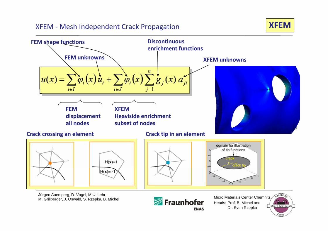
XFEM ‐Mesh Independent Crack Propagation XFEM
FEM shape functions
FEM unknowns
Discontinuousenrichment functions
XFEM unknowns
FEMdisplacement
XFEMHeaviside enrichmentdisplacement
all nodesHeaviside enrichmentsubset of nodes
Crack crossing an element Crack tip in an element
Jürgen Auersperg D Vogel M U LehrJürgen Auersperg, D. Vogel, M.U. Lehr, M. Grillberger, J. Oswald, S. Rzepka, B. Michel Micro Materials Center Chemnitz
Heads: Prof. B. Michel andDr. Sven Rzepka
BEoL Stack of an IC – Cracking/Delamination ‐ Locations and Impacts
Near-chip-edge cracks under Chip Package Interaction (CPI)
Crack stop structure
Near-bump cracking during reflow(NBC)
Leadfree Copper Pillars
Jürgen Auersperg D Vogel M U LehrJürgen Auersperg, D. Vogel, M.U. Lehr, M. Grillberger, J. Oswald, S. Rzepka, B. Michel Micro Materials Center Chemnitz
Heads: Prof. B. Michel andDr. Sven Rzepka
Chip Package Interaction (CPI)
Near-chip-edge cracks
Micro Materials Center ChemnitzHeads: Prof. B. Michel and
Dr. Sven Rzepka
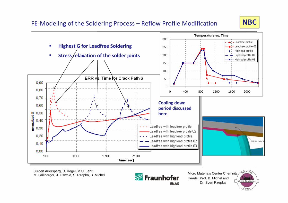
BEoL Stack of an IC – Near‐Bump‐Cracks – Region of Interest NBC
LID adhesive
Packaged FE‐model(eight symmetric model)
LID adhesive
TIM1
Die
Underfill
PI layerNi layerBEoL stack region
Board
Soldermask
HMT solderUnderfill
Soldermask
LJT solder
gap
Jürgen Auersperg D Vogel M U Lehr
Boardpad
Jürgen Auersperg, D. Vogel, M.U. Lehr, M. Grillberger, J. Oswald, S. Rzepka, B. Michel Micro Materials Center Chemnitz
Heads: Prof. B. Michel andDr. Sven Rzepka
3D BEoL Stack Part‐model – Submodeling with Substructures NBC
Substructure
Finite elelement characteristic size in BEoL‐stack
Substructure region
< nm
Replacement of the finest (1x) structures b s perelements (repeatedl sed) leads
Substructure region
by superelements (repeatedly used) leads to a dramatically reduced model size(by factor 3),
Jürgen Auersperg D Vogel M U Lehr
complete model(with and without element edges)
vias andmetal traces
Jürgen Auersperg, D. Vogel, M.U. Lehr, M. Grillberger, J. Oswald, S. Rzepka, B. Michel Micro Materials Center Chemnitz
Heads: Prof. B. Michel andDr. Sven Rzepka
3d Local Model of a BEoL Part – Crack Introduced ‐ SubModeling NBC
Global model
Submodel
Initial crack
Jürgen Auersperg D Vogel M U LehrJürgen Auersperg, D. Vogel, M.U. Lehr, M. Grillberger, J. Oswald, S. Rzepka, B. Michel Micro Materials Center Chemnitz
Heads: Prof. B. Michel andDr. Sven Rzepka
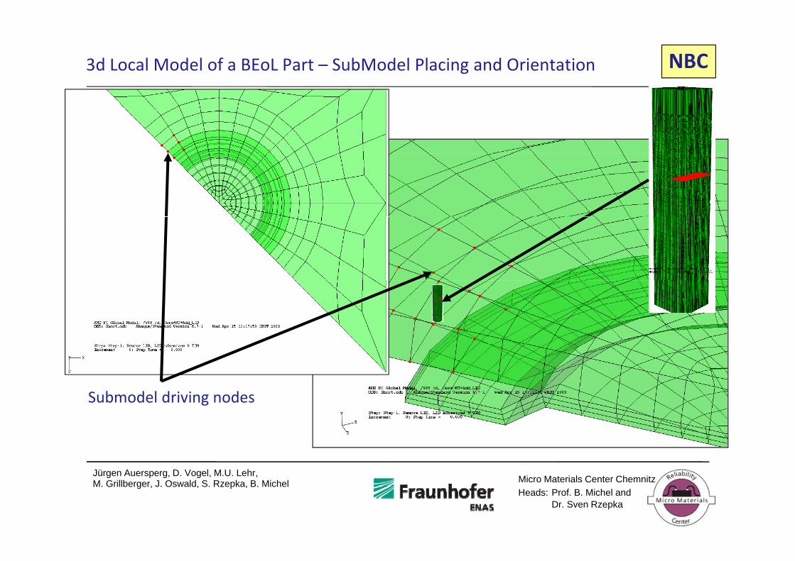
3d Local Model of a BEoL Part – SubModel Placing and Orientation NBC
Submodel driving nodes
Jürgen Auersperg D Vogel M U LehrJürgen Auersperg, D. Vogel, M.U. Lehr, M. Grillberger, J. Oswald, S. Rzepka, B. Michel Micro Materials Center Chemnitz
Heads: Prof. B. Michel andDr. Sven Rzepka
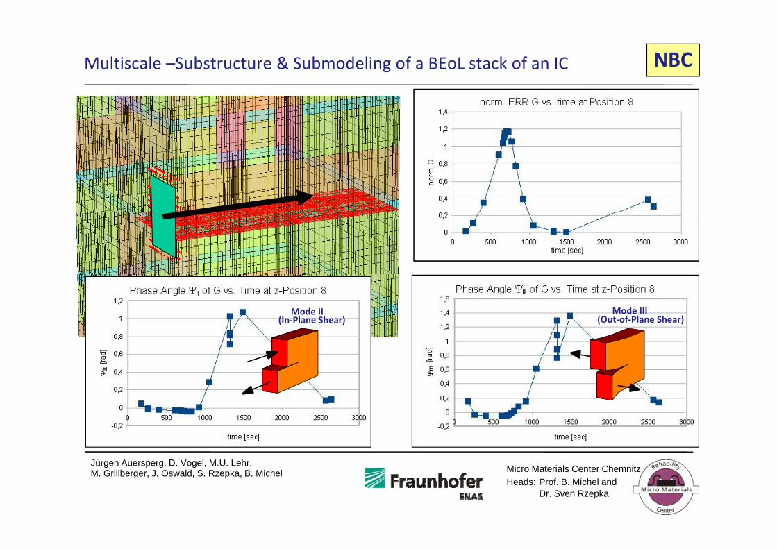
Multiscale –Substructure & Submodeling of a BEoL stack of an IC NBC
Mode II(In‐Plane Shear)
Mode III(Out‐of‐Plane Shear)
Jürgen Auersperg D Vogel M U LehrJürgen Auersperg, D. Vogel, M.U. Lehr, M. Grillberger, J. Oswald, S. Rzepka, B. Michel Micro Materials Center Chemnitz
Heads: Prof. B. Michel andDr. Sven Rzepka
Multiscale –Substructure & Submodeling of a BEoL stack of an IC NBC
C k d i i f l h k fCrack driving force along the crack front
Results:
• Find most critical places with
• Material interface delamination
Jürgen Auersperg D Vogel M U Lehr
Material interface delaminationand/or
• Cohesive fracture of material
Jürgen Auersperg, D. Vogel, M.U. Lehr, M. Grillberger, J. Oswald, S. Rzepka, B. Michel Micro Materials Center Chemnitz
Heads: Prof. B. Michel andDr. Sven Rzepka
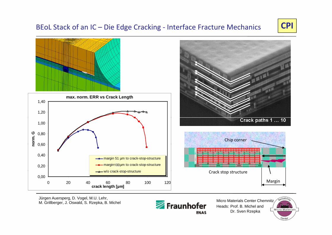
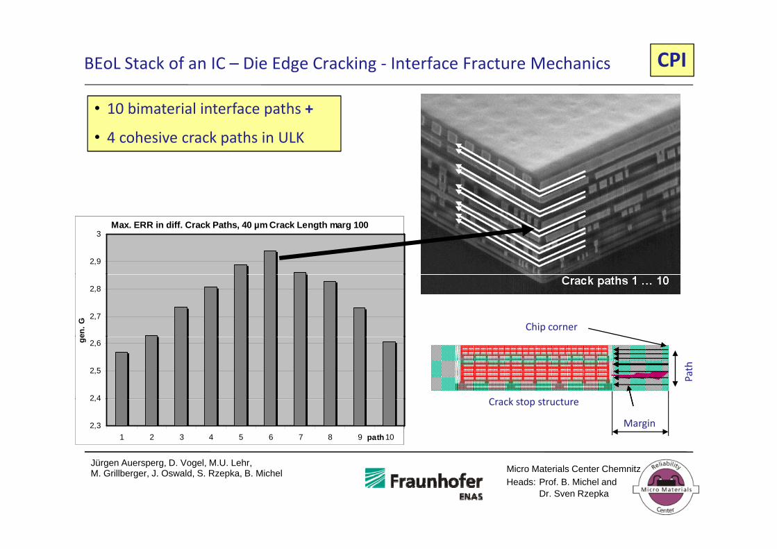
BEoL Stack of an IC – Die Edge Cracking ‐ Interface Fracture Mechanics CPI
max. norm. ERR vs Crack Length
1,20
1,40max. norm. ERR vs Crack Length
1,20
1,40
Chip corner0 60
0,80
1,00
orm
. G
0 60
0,80
1,00
orm
. G
C k t t t0,20
0,40
0,60n
margin 51 µm to crack-stop-structure
margin 51 µm to crack-stop-structure
w/o crack stop structure0,20
0,40
0,60n
margin 51 µm to crack-stop-structure
margin 51 µm to crack-stop-structure
w/o crack stop structure
Jürgen Auersperg D Vogel M U Lehr
Margin
Crack stop structure0,00
0 20 40 60 80 100 120crack length [µm]
w/o crack-stop-structure0,00
0 20 40 60 80 100 120crack length [µm]
w/o crack-stop-structure
Jürgen Auersperg, D. Vogel, M.U. Lehr, M. Grillberger, J. Oswald, S. Rzepka, B. Michel Micro Materials Center Chemnitz
Heads: Prof. B. Michel andDr. Sven Rzepka
BEoL Stack of an IC – Die Edge Cracking ‐ Interface Fracture Mechanics CPI
Jürgen Auersperg D Vogel M U LehrJürgen Auersperg, D. Vogel, M.U. Lehr, M. Grillberger, J. Oswald, S. Rzepka, B. Michel Micro Materials Center Chemnitz
Heads: Prof. B. Michel andDr. Sven Rzepka
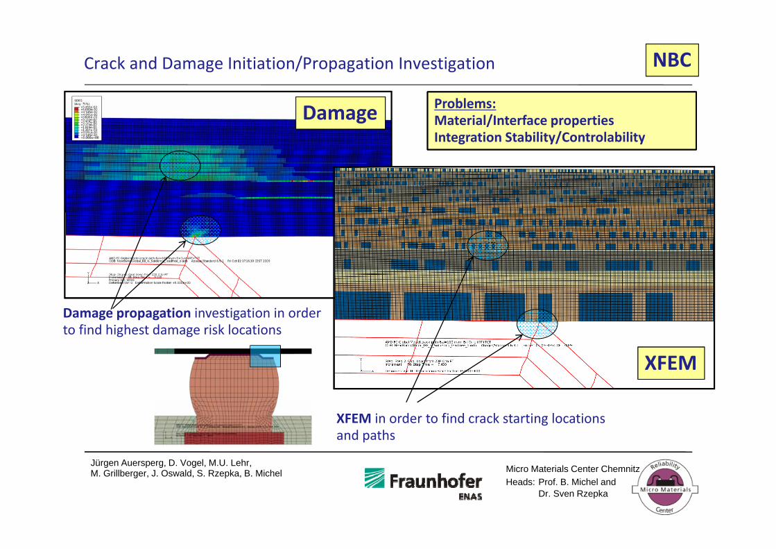
Crack and Damage Initiation/Propagation Investigation NBC
Jürgen Auersperg, D. Vogel, M.U. Lehr, M. Grillberger, J. Oswald, S. Rzepka, B. Michel Micro Materials Center Chemnitz
Heads: Prof. B. Michel andDr. Sven Rzepka
3D I t ti TSV d BE L3D‐Integration – TSV and BEoL
Cracking/Delamination risks during BEoL‐manufacturing on top of TSVs?
Micro Materials Center ChemnitzHeads: Prof. B. Michel and
Dr. Sven Rzepka
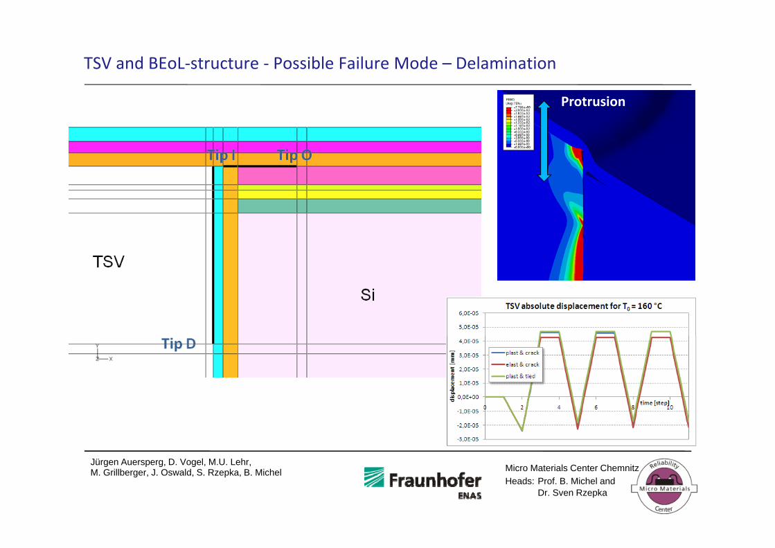
TSV and BEoL‐structure
Protrusion
Jürgen Auersperg D Vogel M U LehrJürgen Auersperg, D. Vogel, M.U. Lehr, M. Grillberger, J. Oswald, S. Rzepka, B. Michel Micro Materials Center Chemnitz
Heads: Prof. B. Michel andDr. Sven Rzepka
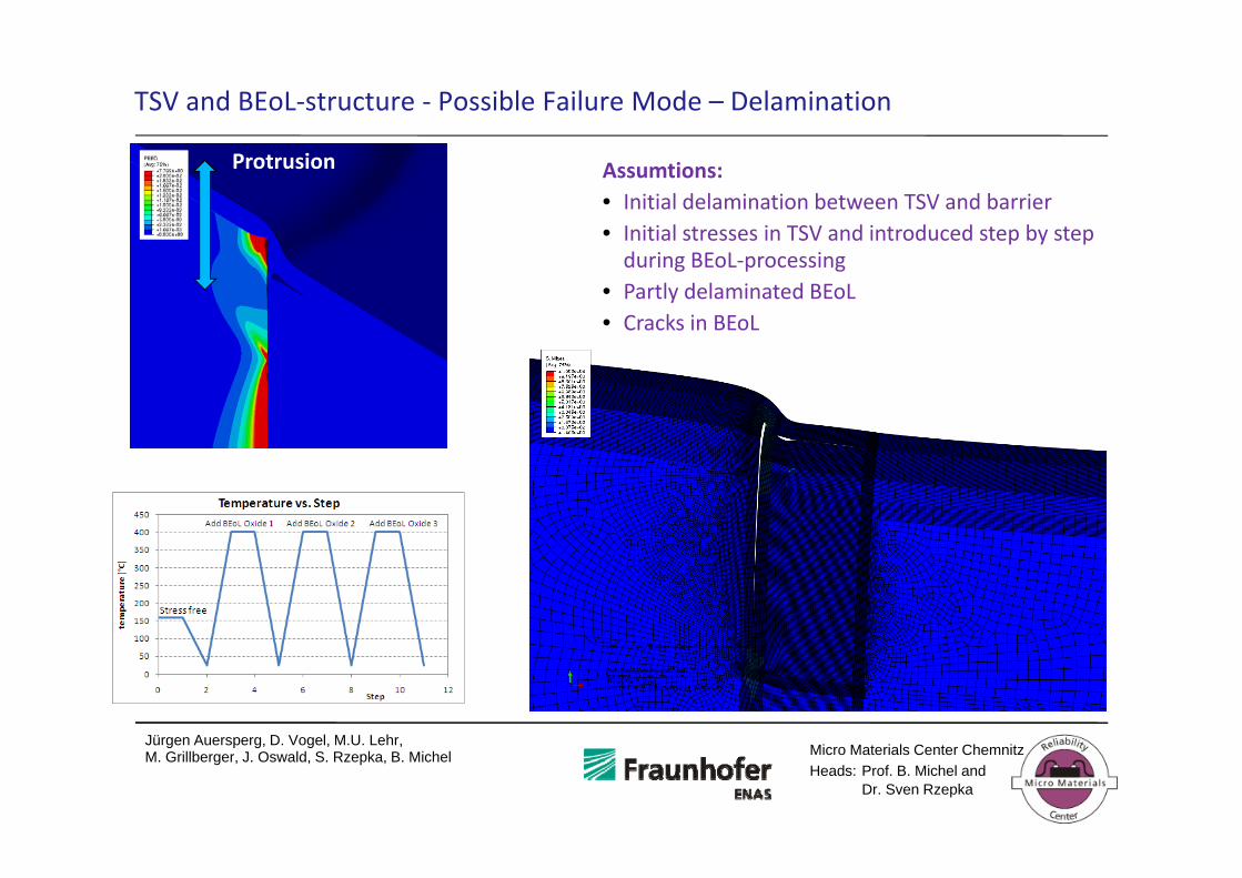
TSV and BEoL‐structure ‐ Possible Failure Mode – Delamination
Protrusion
Jürgen Auersperg D Vogel M U LehrJürgen Auersperg, D. Vogel, M.U. Lehr, M. Grillberger, J. Oswald, S. Rzepka, B. Michel Micro Materials Center Chemnitz
Heads: Prof. B. Michel andDr. Sven Rzepka
TSV and BEoL‐structure ‐ Possible Failure Mode – Delamination
Protrusion Assumtions:• Initial delamination between TSV and barrier• Initial stresses in TSV and introduced step by stepInitial stresses in TSV and introduced step by step during BEoL‐processing
• Partly delaminated BEoL• Cracks in BEoL
Jürgen Auersperg D Vogel M U LehrJürgen Auersperg, D. Vogel, M.U. Lehr, M. Grillberger, J. Oswald, S. Rzepka, B. Michel Micro Materials Center Chemnitz
Heads: Prof. B. Michel andDr. Sven Rzepka
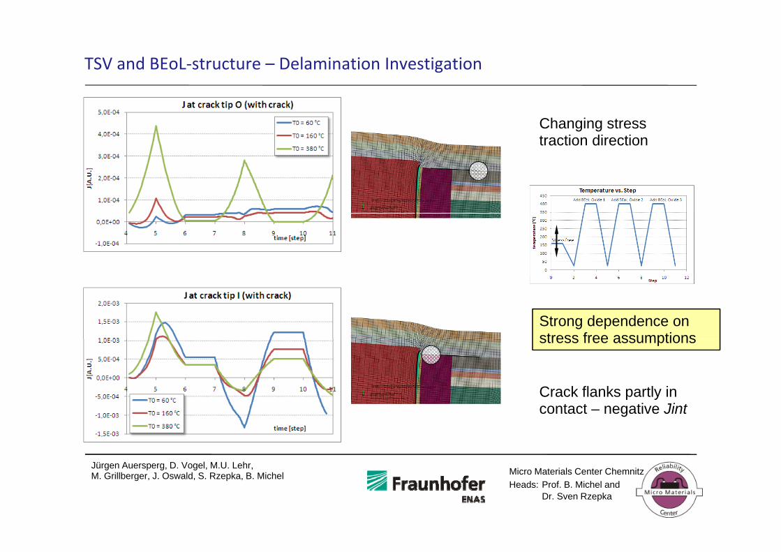
TSV and BEoL‐structure – Delamination Investigation
Changing stress traction direction
Strong dependence on stress free assumptions
Crack flanks partly in
stress free assumptions
Jürgen Auersperg D Vogel M U Lehr
contact – negative Jint
Jürgen Auersperg, D. Vogel, M.U. Lehr, M. Grillberger, J. Oswald, S. Rzepka, B. Michel Micro Materials Center Chemnitz
Heads: Prof. B. Michel andDr. Sven Rzepka
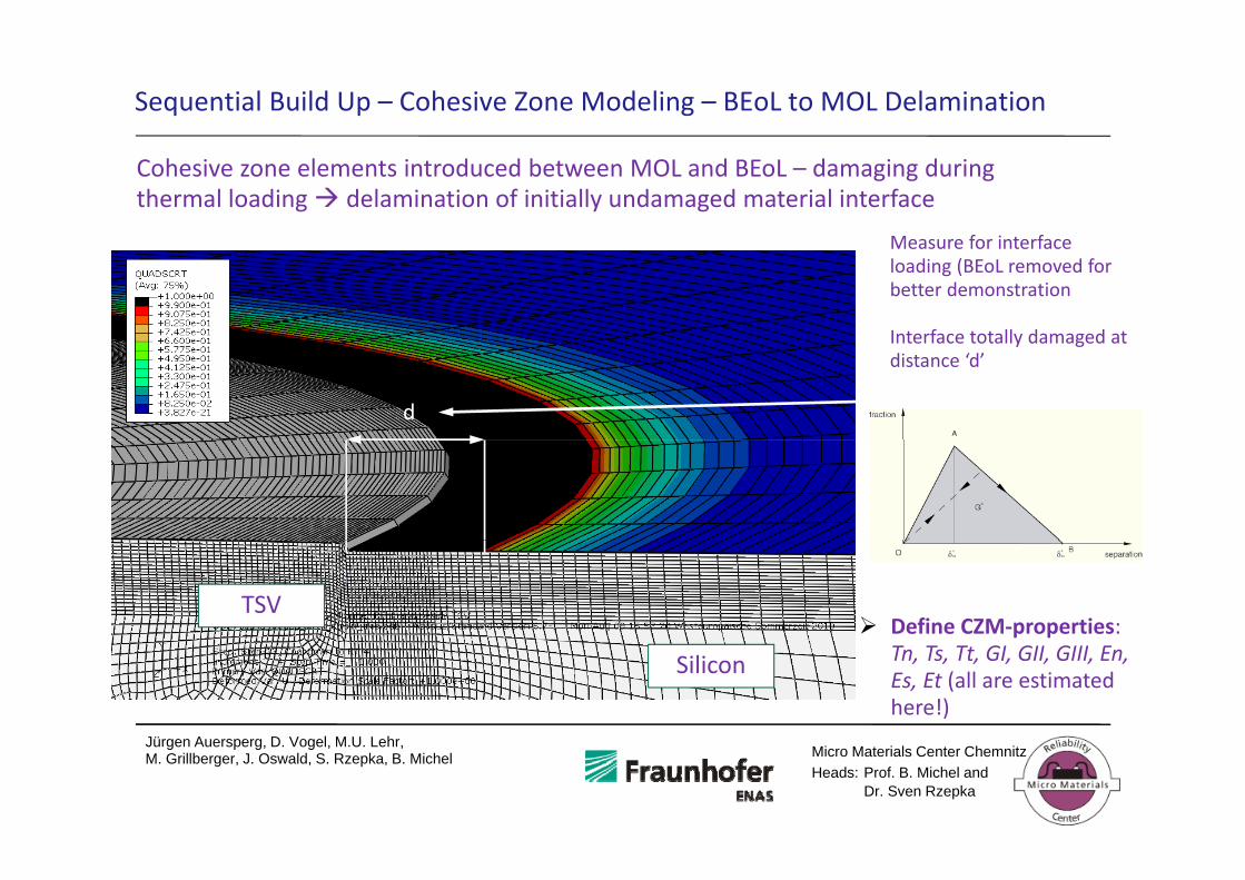
Sequential Build Up – Cohesive Zone Modeling – BEoL to MOL Delamination
Measure for interface
Cohesive zone elements introduced between MOL and BEoL – damaging during thermal loading delamination of initially undamaged material interface
Measure for interface loading (BEoL removed for better demonstration
Interface totally damaged atInterface totally damaged at distance ‘d’
d
TSV Define CZM‐properties:
Jürgen Auersperg D Vogel M U Lehr
Silicon Tn, Ts, Tt, GI, GII, GIII, En, Es, Et (all are estimated here!)
Jürgen Auersperg, D. Vogel, M.U. Lehr, M. Grillberger, J. Oswald, S. Rzepka, B. Michel Micro Materials Center Chemnitz
Heads: Prof. B. Michel andDr. Sven Rzepka
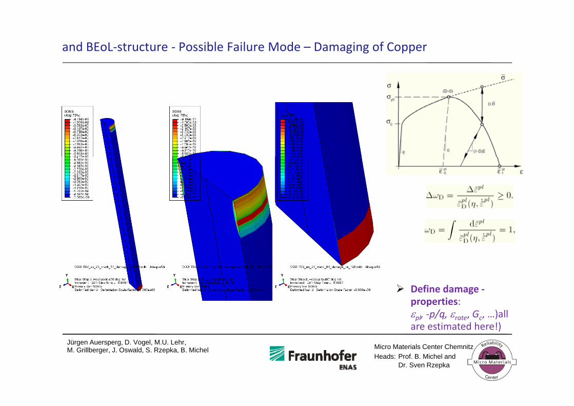
and BEoL‐structure ‐ Possible Failure Mode – Damaging of Copper
Define damage ‐
Jürgen Auersperg D Vogel M U Lehr
properties:pl, ‐p/q, rate, Gc, …)all are estimated here!)
Jürgen Auersperg, D. Vogel, M.U. Lehr, M. Grillberger, J. Oswald, S. Rzepka, B. Michel Micro Materials Center Chemnitz
Heads: Prof. B. Michel andDr. Sven Rzepka
M t i l P t D t i tiMaterial Property Determination
Size Dependent Material Behavior
Micro Materials Center ChemnitzHeads: Prof. B. Michel and
Dr. Sven Rzepka
Material Behavior ‐Measure Required Properties
Dynamical‐Mechanical Analysis (DMA) Thermomechanical Analysis (TMA) Creep data eval. (Solder)
Temp.dep. creep data (Epoxy) Stress relaxation data (Epoxy) Poisson’s ratio eval.Temp.dep. creep data (Epoxy) Stress relaxation data (Epoxy) Poisson s ratio eval.
Jürgen Auersperg D Vogel M U LehrJürgen Auersperg, D. Vogel, M.U. Lehr, M. Grillberger, J. Oswald, S. Rzepka, B. Michel Micro Materials Center Chemnitz
Heads: Prof. B. Michel andDr. Sven Rzepka
H. Walter, J. Auersperg
Nanoindentation in low‐K DielectricsBump side
BEoL stack
7 µm
Thin layers
Chip side
7 µm
For TSV:
800
1000
1200
1400
SimN] 800
1000
1200
1400
SimN]
F, uF, u • Initial yield stress• Hardening behavior
200
400
600
MeasurementE=145, sy=1600-10000Experiment
Sim
Forc
e [µ
200
400
600
MeasurementE=145, sy=1600-10000Experiment
Sim
Forc
e [µ
Intenter
Thin Layer
S b t t
Intenter
Thin Layer
S b t t
a de g be a o
-200
00 20 40 60 80
Distance [nm]
-200
00 20 40 60 80
Distance [nm]
SubstrateSubstrate
Experiment Simulation Agreement
Jürgen Auersperg D Vogel M U Lehr
Parameter – extraction only possible by coupled Sim & Exp
Jürgen Auersperg, D. Vogel, M.U. Lehr, M. Grillberger, J. Oswald, S. Rzepka, B. Michel Micro Materials Center Chemnitz
Heads: Prof. B. Michel andDr. Sven Rzepka
Raul Mrosko, Saskia Huber, O. Wittler
TSV Copper – YOUNGs Modulus by nano‐Indentation
46,405
P13 Messung 3
d e m o d e m o d e m o d e m o d e m od e m o d e m o d e m o d e m o d e m o
120
140
P13 Messung 3
46,400
)
d e m o d e m o d e m o d e m o d e m o
d e m o d e m o d e m o d e m o d e m o
d e m o d e m o d e m o d e m o d e m o
d e m o d e m o d e m o d e m o d e m o
80
100
Er(G
Pa)
46,395
Y(m
m)
d e m o d e m o d e m o d e m o d e m o
d e m o d e m o d e m o d e m o d e m o
d e m o d e m o d e m o d e m o d e m o
d e m o d e m o d e m o d e m o d e m o
82 275 82 270 82 265 82 26040
60
46390
d e m o d e m o d e m o d e m o d e m od e m o d e m o d e m o d e m o d e m o
-82,275 -82,270 -82,265 -82,260
X(mm)
-82,275 -82,270 -82,265 -82,26046,390
X(mm)
Jürgen Auersperg D Vogel M U LehrJürgen Auersperg, D. Vogel, M.U. Lehr, M. Grillberger, J. Oswald, S. Rzepka, B. Michel Micro Materials Center Chemnitz
Heads: Prof. B. Michel andDr. Sven Rzepka
Copper Material Behavior– Properties Necessary
Necessary to know:
• Young's‐modulus dep. On Temperature
• Initial yield stressInitial yield stress
• Hardening vs. plastic strains
• Regarding TSV: initial stress state
Xi Liu, Qiao Chen, Pradeep Dixit, Ritwik Chatterjee, Rao R. Tummala, and Suresh K. Sitaraman, Failure Mechanisms and Optimum Design for Electroplated Copper Through‐Silicon Vias(TSV), 2009 Electronic Components and Technology
fConference, pp. 624 ‐ 629
Jürgen Auersperg D Vogel M U LehrJürgen Auersperg, D. Vogel, M.U. Lehr, M. Grillberger, J. Oswald, S. Rzepka, B. Michel Micro Materials Center Chemnitz
Heads: Prof. B. Michel andDr. Sven Rzepka
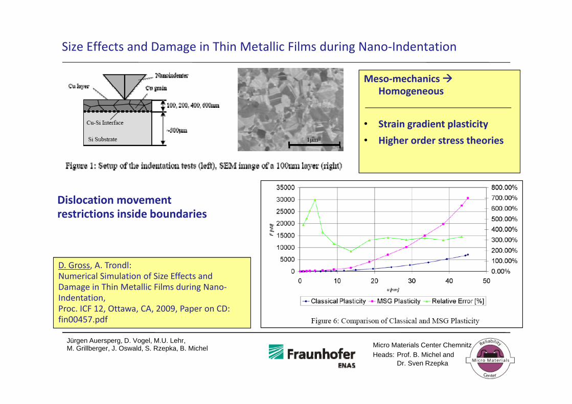
Size Effects and Damage in Thin Metallic Films during Nano‐Indentation
Meso‐mechanics Homogeneous
• Strain gradient plasticity
• Higher order stress theories
Dislocation movementDislocation movement restrictions inside boundaries
D. Gross, A. Trondl:Numerical Simulation of Size Effects and Damage in Thin Metallic Films during Nano‐
Jürgen Auersperg D Vogel M U Lehr
Indentation,Proc. ICF 12, Ottawa, CA, 2009, Paper on CD: fin00457.pdf
Jürgen Auersperg, D. Vogel, M.U. Lehr, M. Grillberger, J. Oswald, S. Rzepka, B. Michel Micro Materials Center Chemnitz
Heads: Prof. B. Michel andDr. Sven Rzepka
D d F t T h Ch t i tiDamage and Fracture Toughness Characterization
Size Dependent Material Behavior
Micro Materials Center ChemnitzHeads: Prof. B. Michel and
Dr. Sven Rzepka
Interface Fracture Toughness Tests
P
Pull‐off test schematic of substrate, interface and pull stud
Modified CT‐specimen Peel test
Jürgen Auersperg D Vogel M U Lehr
Pull‐out test Brazilian disk specimen Superlayer adhesion test
A.A. Volinsky et al. / Acta Materialia 50 (2002) 441–466
Jürgen Auersperg, D. Vogel, M.U. Lehr, M. Grillberger, J. Oswald, S. Rzepka, B. Michel Micro Materials Center Chemnitz
Single Leg BendingSymmetric Double Cantilever Beam
4‐point bending
Asymmetric DCB
Asymmetric End‐Notched FlexureEnd‐Notched Flexure
Mill H 2000
Double Cantilever BeamCenter Cracked Beam
Jürgen Auersperg D Vogel M U Lehr
Sundaraman, Sitaraman 1997Yeung, Lam, Yuen 2000
Miller, Ho 2000
Jürgen Auersperg, D. Vogel, M.U. Lehr, M. Grillberger, J. Oswald, S. Rzepka, B. Michel Micro Materials Center Chemnitz
Heads: Prof. B. Michel andDr. Sven Rzepka
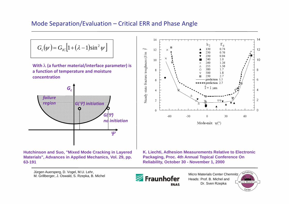
Mode Separation/Evaluation – Critical ERR and Phase Angle
failure regionregion
Measured fracture toughness
Calculated crack loading
Jürgen Auersperg D Vogel M U LehrJürgen Auersperg, D. Vogel, M.U. Lehr, M. Grillberger, J. Oswald, S. Rzepka, B. Michel Micro Materials Center Chemnitz
Heads: Prof. B. Michel andDr. Sven Rzepka
Mode Separation/Evaluation – Critical ERR and Phase Angle
2sin11 ICc GG
With (a further material/interface parameter) is a function of temperature and moisture concentration
G() i i i i
Gc
failure i G() initiation
G()no initiation
region
Jürgen Auersperg D Vogel M U Lehr
K. Liechti, Adhesion Measurements Relative to Electronic Packaging, Proc. 4th Annual Topical Conference On Reliability, October 30 - November 1, 2000
Hutchinson and Suo, "Mixed Mode Cracking in Layered Materials", Advances in Applied Mechanics, Vol. 29, pp. 63-191
Jürgen Auersperg, D. Vogel, M.U. Lehr, M. Grillberger, J. Oswald, S. Rzepka, B. Michel Micro Materials Center Chemnitz
Heads: Prof. B. Michel andDr. Sven Rzepka
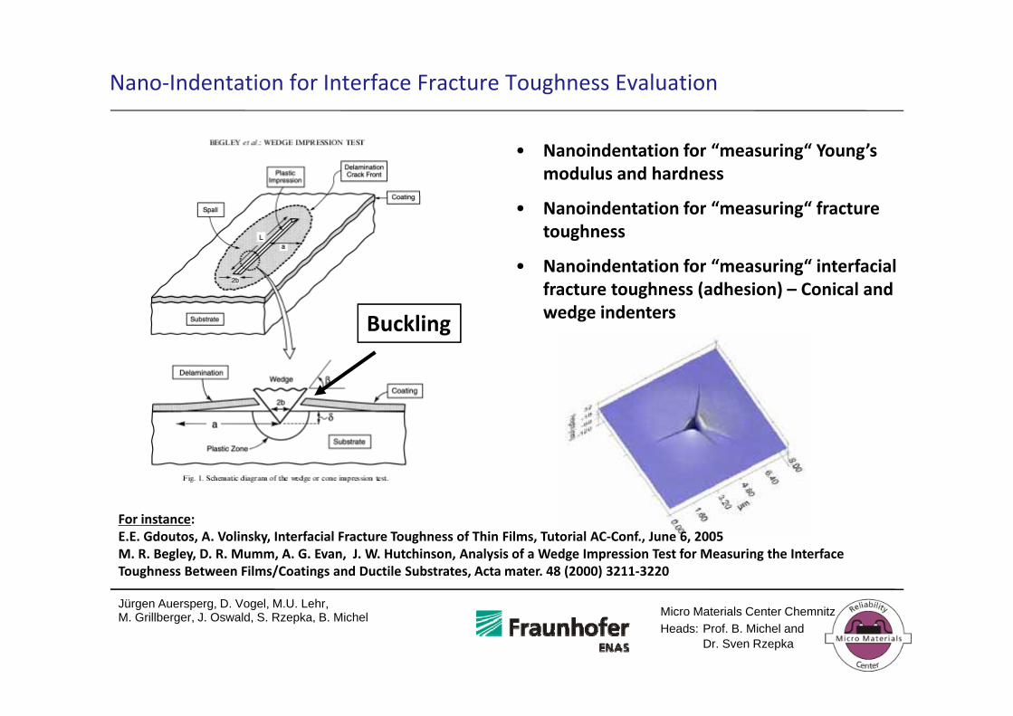
Nano‐Indentation for Interface Fracture Toughness Evaluation
• Nanoindentation for “measuring“ Young’s modulus and hardness
• Nanoindentation for “measuring“ fracture toughness
• Nanoindentation for “measuring“ interfacial fracture toughness (adhesion) – Conical and wedge indentersBuckling
For instance:
Jürgen Auersperg D Vogel M U Lehr
For instance:E.E. Gdoutos, A. Volinsky, Interfacial Fracture Toughness of Thin Films, Tutorial AC‐Conf., June 6, 2005M. R. Begley, D. R. Mumm, A. G. Evan, J. W. Hutchinson, Analysis of a Wedge Impression Test for Measuring the Interface Toughness Between Films/Coatings and Ductile Substrates, Acta mater. 48 (2000) 3211‐3220
Jürgen Auersperg, D. Vogel, M.U. Lehr, M. Grillberger, J. Oswald, S. Rzepka, B. Michel Micro Materials Center Chemnitz
Heads: Prof. B. Michel andDr. Sven Rzepka
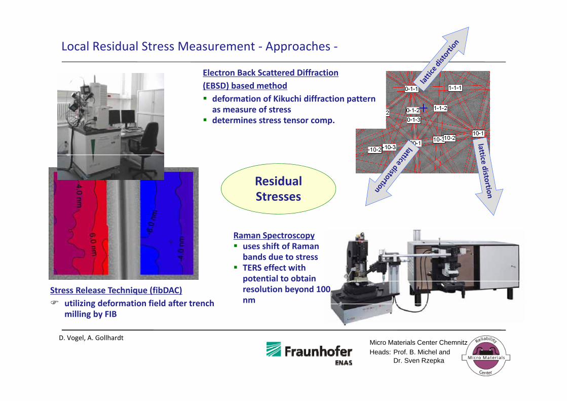
St St t D t i ti /V ifi tiStress State Determination/Verification
Fitting modeling assumption with experimental results
Micro Materials Center ChemnitzHeads: Prof. B. Michel and
Dr. Sven Rzepka
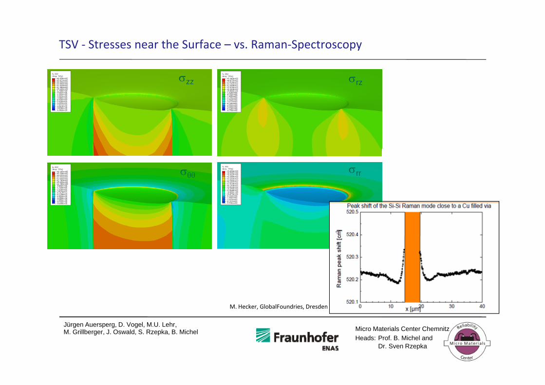
TSV ‐ Stresses near the Surface – vs. Raman‐Spectroscopy
zz rz
rr
Jürgen Auersperg D Vogel M U Lehr
M. Hecker, GlobalFoundries, Dresden
Jürgen Auersperg, D. Vogel, M.U. Lehr, M. Grillberger, J. Oswald, S. Rzepka, B. Michel Micro Materials Center Chemnitz
Heads: Prof. B. Michel andDr. Sven Rzepka
Surface vs. Midd‐Stress rr
Surface - rr
Middle -
Jürgen Auersperg D Vogel M U Lehr
Middle - rr
Jürgen Auersperg, D. Vogel, M.U. Lehr, M. Grillberger, J. Oswald, S. Rzepka, B. Michel Micro Materials Center Chemnitz
Heads: Prof. B. Michel andDr. Sven Rzepka
Summary
M ltil l FE d lli f k i BE L St kt Multilevel FE‐modelling of cracks in BEoL‐Struktures
For Chip Package Interaction and
fl l df b i Reflow ‐ leadfree bumping
Goal: Reliability enhancement
Utilizing fracture mechanics concepts (cohesive and adhesive) and/or
Damage mechanics approaches
Jürgen Auersperg D Vogel M U LehrJürgen Auersperg, D. Vogel, M.U. Lehr, M. Grillberger, J. Oswald, S. Rzepka, B. Michel Micro Materials Center Chemnitz
Heads: Prof. B. Michel andDr. Sven Rzepka
What we need
Intensive experimental work necessary for
Evaluation of residual stresses from manufacturing,
Evaluation of the material behavior (constitutive, size dependent)
Characterization of the damage behavior of materials
Characterization of strength/toughness properties (fracture mechanics characterization) of materials and materials interfaces
Verification of simulation results
Extensive simulation work necessary
Huge simulation models and computing resources
Jürgen Auersperg D Vogel M U Lehr
Theoretical work – delamination und fracture (CZM, XFEM), materials behavior (SGPM)
Jürgen Auersperg, D. Vogel, M.U. Lehr, M. Grillberger, J. Oswald, S. Rzepka, B. Michel Micro Materials Center Chemnitz
Heads: Prof. B. Michel andDr. Sven Rzepka
What we Need for Helpful Simulation Results
Residual stress characterization
Damage and fracture characterization
Material behavior and property characterization
Jürgen Auersperg D Vogel M U Lehr
Simulation results verification
Jürgen Auersperg, D. Vogel, M.U. Lehr, M. Grillberger, J. Oswald, S. Rzepka, B. Michel Micro Materials Center Chemnitz
Heads: Prof. B. Michel andDr. Sven Rzepka
Th k Y f Y Att ti !Thank You for Your Attention!
Micro Materials Center ChemnitzHeads: Prof. B. Michel and