University of Central Florida University of Central Florida STARS STARS Electronic Theses and Dissertations, 2004-2019 2008 Design, Characterization And Compact Modeling Of Novel Silicon Design, Characterization And Compact Modeling Of Novel Silicon Controlled Rectifier (scr)-based Devices For Electrostatic Discha Controlled Rectifier (scr)-based Devices For Electrostatic Discha Lifang Lou University of Central Florida Part of the Electrical and Electronics Commons Find similar works at: https://stars.library.ucf.edu/etd University of Central Florida Libraries http://library.ucf.edu This Doctoral Dissertation (Open Access) is brought to you for free and open access by STARS. It has been accepted for inclusion in Electronic Theses and Dissertations, 2004-2019 by an authorized administrator of STARS. For more information, please contact [email protected]. STARS Citation STARS Citation Lou, Lifang, "Design, Characterization And Compact Modeling Of Novel Silicon Controlled Rectifier (scr)- based Devices For Electrostatic Discha" (2008). Electronic Theses and Dissertations, 2004-2019. 3597. https://stars.library.ucf.edu/etd/3597
Transcript
University of Central Florida University of Central Florida
STARS STARS
Electronic Theses and Dissertations, 2004-2019
2008
Design, Characterization And Compact Modeling Of Novel Silicon Design, Characterization And Compact Modeling Of Novel Silicon
Controlled Rectifier (scr)-based Devices For Electrostatic Discha Controlled Rectifier (scr)-based Devices For Electrostatic Discha
Lifang Lou University of Central Florida
Part of the Electrical and Electronics Commons
Find similar works at: https://stars.library.ucf.edu/etd
University of Central Florida Libraries http://library.ucf.edu
This Doctoral Dissertation (Open Access) is brought to you for free and open access by STARS. It has been accepted
for inclusion in Electronic Theses and Dissertations, 2004-2019 by an authorized administrator of STARS. For more
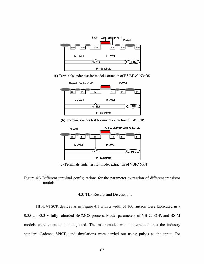
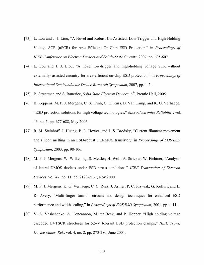
Figure 2.1 Device cross-section view of the uSCR, showing the locations of the Ln and Lp regions and the dimensions associated with the device characteristic.
When the anode of the device is biased positively with respect to the cathode, the P+/N-
Well junction and the P-Well/N+ junction are forward biased while the center junction, P-
Well/N-Well, is under reverse bias. Most of the forward voltage drops across the P-Well/N-Well
junction. The current level is small at the beginning since the supply of electrons and holes to the
27
center junction is restricted by the reverse-biased junction on either side [75]. If holes are
injected from P+ to N-Well and will recombine with electrons in N-Well region to maintain
space charge neutrality, the supply of electrons in current situation is severely restricted since N-
Well region is terminated in the reverse-biased P-Well/N-Well junction. It is the same thing to
electrons injected from N+ to P-Well region. The P-Well/N-Well junction is the blocking
junction. The supply of electrons and holes are from the thermal generation of electron-hole pairs
at the center junction. As a result, the total current is approximately the reverse saturation current
of the center junction and the SCR device is in forward-blocking state. The reverse saturation
current passing through the center junction will be multiplied by the carrier multiplication due to
impact ionization over a fairly broad range of the voltage. As shown in Figure 2.2,
C PNP PNP E PNP co PNPI I Iα− − −= + (2.1)
( )1B PNP E PNP C PNP PNP E PNP co PNPI I I I Iα− − − − −= − = − − (2.2)
where αPNP is the current transport factor of PNP transistor and Ico-PNP is the collector-base
reverse saturation current of PNP transistor,
when multiplied by the multiplication factor, M,
( )C PNP PNP E PNP co PNPI M I Iα− − −= ⋅ + (2.3)
( )1B PNP PNP E PNP co PNPI M I M Iα− − −= − ⋅ − ⋅ (2.4)
similarly,
( )C NPN NPN E NPN co NPNI M I Iα− − −= ⋅ + (2.5)
where αNPN the current transport factor of PNP transistor and Ico-NPN is the collector-base reverse
saturation current of NPN transistor, assuming MPNP=MNPN. Since
28
B PNP SUB PNP C NPNI I I− − −+ = (2.6)
E PNP A SUB PNPI I I− −= − (2.7)
E NPN A SUB NPNI I I− −= − (2.8)
replacing Equation (2.4), (2.5), (2.7), (2.8) in Equation (2.6), it will have:
( )1 ( )
co PNP co NPN PNP SUB PNP NPN SUB NPNA
PNP NPN
M I I M I M II
Mα αα α
− − − −+ − −=
− + (2.9)
When carrier multiplication happens in the center junction, many electrons are swept into N-
Well region and holes into P-Well region. This process provides the majority carriers to these
regions needed for increased injection by the emitter junctions. As derived in Equation (2.9),
breakdown occurs at the center blocking junction when
( ) 1PNP NPNM α α+ → (2.10)
When the bias voltage increases, the depletion region of the P-Well/N-Well junction will expand,
which means the base widths of both PNP and NPN transistors will be narrowed. Since αPNP and
αNPN increase as the base widths decrease, the device triggering can occur by the effect of base-
width narrowing. And just moderate narrowing can increase the alphas enough to trigger the
device with the contribution of avalanche multiplication. As M(αPNP +αNPN) approaches unity,
many holes injected into N-Well region survive to be swept across center blocking junction into
P-Well region. This helps to feed the recombination in P-Well region and to support the injection
of holes into N+ region. Similarly, the elections injected in to P-Well region and collected by N-
Well will supply the injection of electrons into P+ region. The transfer of injected carriers across
the center junction is regenerative which means a greater supply of electrons to N-Well allows a
29
greater injection of holes from P+ and this greater injection of holes further feeds P-Well by
transistor action. The process continues to repeat itself to push the device to be triggered in the
end.
From another point of view, when the bias voltage increases, the reverse saturation
current will increase due to impact ionization. This current will flow through the two substrate
resistances, RN-Well and RP-Well (see Figure 2.1 and Figure 2.2), to raise the base-emitter voltages
of both transistors. As long as the voltage drop on the base-emitter junction is greater than about
0.7 V, the PNP emitter and the NPN emitter would be allowed to inject a large number of holes
and electrons, respectively, and the positive feedback regenerative mechanism is then initiated
and the SCR device becomes active. Both PNP and NPN transistors are working in forward
active mode now.
When the avalanche multiplication happens in the center junction, the primary collector
current, IC-PNP and IC-NPN, are multiplied by M.
( ) ( )A C PNP C NPN PNP E PNP co PNP NPN E NPN co NPNI M I M I M I I M I Iα α− − − − − −= ⋅ + ⋅ = ⋅ + + ⋅ + (2.11)
Equation (2.11) can be rewritten as:
1 E PNP E NPN co PNP co NPNPNP NPN
A A A
I I I IM I I I
α α− − − −+= + +
(2.12)
M can also be expressed as [84]:
1 1n
BC
BRK
VM V
⎛ ⎞= − ⎜ ⎟
⎝ ⎠ (2.13)
VBRK is the breakdown voltage of the center junction which is also the base-collector junction of
both PNP and NPN transistors, VBC is the voltage drop across this junction, and n is typically
30
equal to 2. By equaling Equation (2.12) with Equation (2.13), the trigger voltage, VT, will be
obtained as:
1
1n
E PNP E NPN co PNP co NPNT BC BRK PNP NPN
A A A
I I I IV V VI I I
α α− − − −⎛ ⎞+= = ⋅ − − −⎜ ⎟
⎝ ⎠ (2.14)
Cathode
Anode
RN-Well
RP-Well
PNP
NPN
IA
ISUB-PNP
IB - PNP
ISUB -NPN
IC-PNP
IE-NPN
IE-PNP
IC-NPN
IB-NPN
IA
Figure 2.2 The equivalent circuit of the SCR device.
As derived in Equation (2.14), the breakdown voltage of the blocking junction controls
the trigger voltage. In a typical low-triggering SCR without an external trigger circuit [62], the
blocking junction is the P-Well/N-Well junction whose breakdown voltage is fairly high. To
reduce the trigger voltage, the modified lateral SCR (MLSCR) [62] shown in Figure 2.1 is made
by adding an N+ diffusion across the P-Well/N-Well junction. In such a device, the N+/P-Well
junction controls the trigger voltage. In order to develop the new uSCR for further reducing the
31
trigger voltage, the N-type ESD (NESD) and P-type lightly-doped drain (PLDD) regions
(regions indicated with dashed lines in Figure 2.1) are added into the MLSCR through the LDD
ion implant step. The lengths, Ln and Lp, depict the NESD and PLDD region extensions. Lx is the
distance between the N+ and P+ regions (see Figure 2.1) and the silicide blocking mask covers
this region for the fully-salicided process. The variation of Ln and Lp is visualized in Figure 2.3.
When these two NESD and PLDD regions touch or overlap with each other (i.e., Ln+Lp ≥ Lx),
the NESD/PLDD junction takes over the N+/P-Well junction and becomes the dominant
blocking junction. The order of magnitude of doping levels for N+, P-Well, NESD and PLDD
are approximately 1020cm-3, 1017cm-3, 1019cm-3 and 1019cm-3, respectively. Since the depletion-
region width of the NESD/PLDD junction is much smaller than that of the N+/P-Well junction
under the same reverse-biased voltage, the former can breakdown at a smaller voltage than the
latter, which is able to make the SCR device triggered at much lower voltage.
P-Well
NESD PLDD
Silicide Blocking Layer
Lx
Ln Lp
Lx=1µm
Ln Lp
Ln Lp
N -Well
PLDD
Lx=1µm
Lx=1µm
Ln+Lp < Lx
Ln+Lp= Lx
Ln+Lp > Lx
Ln LpD5 D6
P-Well
PLDD
Silicide Blocking Layer
Lx
Ln Lp
Lx=1µm
Ln Lp
Ln Lp
N -Well
NESD PLDD
Lx=1µm
Lx=1µm
Ln+Lp < Lx
Ln+Lp= Lx
Ln+Lp > Lx
Ln LpD5 D
P-Well
NESD PLDD
Silicide Blocking Layer
Lx
Ln Lp
Lx=1µm
Ln Lp
Ln Lp
N -Well
PLDD
Lx=1µm
Lx=1µm
Ln+Lp < Lx
Ln+Lp= Lx
Ln+Lp > Lx
Ln LpD5 D6
P-Well
PLDD
Silicide Blocking Layer
Lx
Ln Lp
Lx=1µm
Ln Lp
Ln Lp
N -Well
NESD PLDD
Lx=1µm
Lx=1µm
Ln+Lp < Lx
Ln+Lp= Lx
Ln+Lp > Lx
Ln LpD5 D
Figure 2.3 Schematic diagram showing the different cases of Ln+Lp. Lx always keeps at 1μm.
32
A high and tunable holding voltage is desirable for latch-up immunity. On the
phenomenological level, the holding voltage depends on the degree of space charge
neutralization in the base regions of the p-n-p and n-p-n BJTs due to free carriers injected from
the emitter regions of the two BJTs. Hence, the lateral dimensions associated with the
neutralization area and injection area are the key parameters in designing the holding voltage.
For the uSCR shown in Figure 2.1, the holding voltage is tunable by changing the dimensions D3,
D5, D6 and D8.
For the negative characteristic of the uSCR device, the reverse breakdown and
conducting capability will be different when N-Well electrode is connected in two different ways.
Keeping the terminals, Emitter-NPN and P-Well, connected together as Cathode and tied to
ground, when N-Well is connected to Anode, the reverse breakdown voltage will approximate
the turn-on voltage of forward-biased p-n junction and the conduction current can be relatively
high. When N-Well is left open, the reverse breakdown voltage is about equal to VCEO of the
parasitic PNP BJT and the conducting capability is low. The normal operation of uSCR is to
keep N-Well connected to Anode. The connection way of N-Well open can be used to form a
dual direction SCR [63].
2.3. Experimental Results and Discussions
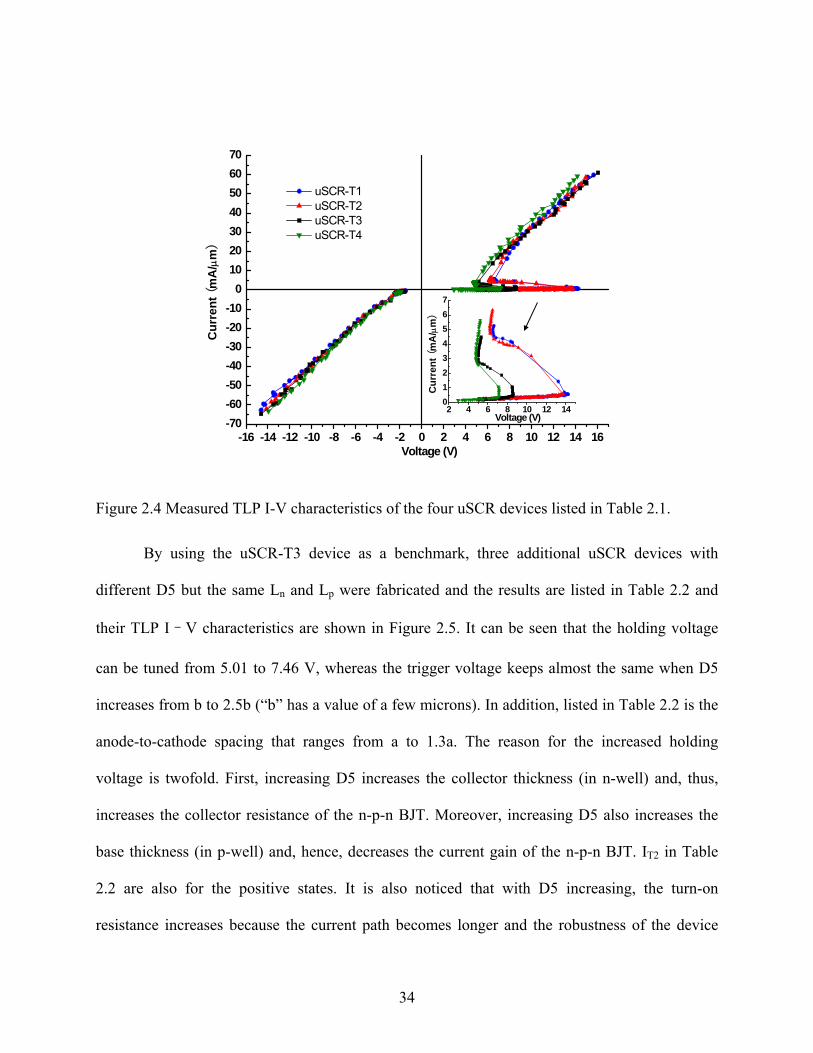
uSCR devices have been fabricated on a 0.35-μm fully-salicided BiCMOS process (see
Table 1.1). Their TLP I-V characteristics are plotted in Figure 2.4. The devices all have a width
of 100 μm and Lx of 1μm, while Ln and Lp are varied. The distance of anode to cathode keeps at
a (a has a value of more than 10 μm).
33
The trigger voltage VT is decreased from 14.24 to 7.16 V when Ln + Lp increases from 0
to 1.5Lx. Note that the trigger voltage is reduced more significantly when Ln + Lp is increased
beyond Lx. The leakage current IL increases with increasing Ln + Lp, but all IL are lower than 10-8
A. The holding voltage VH also decreases with increasing Ln and Lp. The change of Ln and Lp
alters only slightly the slope of the on-state I-V curve. The negative characteristic of the uSCR
devices is like a forward-biased diode. The IT2 listed in Table 2.1 are the failure current levels of
the four uSCRs in the positive operation regions. The ESD robustness of the uSCR in both the
positive and negative operations is high then 60 mA/μm.
When designing a snapback-type device, one of the most important things is to verify the
tolerance of the device for process variation. Even for the same process, the I-V characteristic of
the devices from different lots, wafers and dies will vary. The design goal is to make the device
function ESD protection correctly with the process variation. For the uSCR device, the low
trigger voltage is realized by dimension variation of Ln and Lp, whose tolerance for aligning Ln
and Lp was +/-5% and among the uSCR devices fabricated on four different wafers, alignment-
induced variability in the trigger voltage was with +/- 1.5%.
Table 2.1 Lateral dimensions and TLP measurement results of the four uSCR devices with different Ln + Lp.
a
a
a
a
Cathode( )
Anode to
8.0
1.0
0.1
0.1
(nA)
IL
306
297
490
488
(mA)
IH
≥604.77427.16Ln + Lp = 1.5LxuSCR-T4
≥605.01488.6Ln + Lp = LxuSCR-T3
≥606.155513.4Ln + Lp = 0.5LxuSCR-T2
≥606.55614.24Ln = Lp = 0uSCR-T1
(mA/ )(V)(mA)(V)
IT2VHITVT
Ln, Lp, LxCell Name
a
a
a
a
Cathode( )
Anode to
8.0
1.0
0.1
0.1
(nA)
IL
306
297
490
488
(mA)
IH
≥604.77427.16Ln + Lp = 1.5LxuSCR-T4
≥605.01488.6Ln + Lp = LxuSCR-T3
≥606.155513.4Ln + Lp = 0.5LxuSCR-T2
≥606.55614.24Ln = Lp = 0uSCR-T1
(mA/ )(V)(mA)(V)
IT2VHITVT
Ln, Lp, LxCell Namemμ
mμ
34
Figure 2.4 Measured TLP I-V characteristics of the four uSCR devices listed in Table 2.1.
By using the uSCR-T3 device as a benchmark, three additional uSCR devices with
different D5 but the same Ln and Lp were fabricated and the results are listed in Table 2.2 and
their TLP I–V characteristics are shown in Figure 2.5. It can be seen that the holding voltage
can be tuned from 5.01 to 7.46 V, whereas the trigger voltage keeps almost the same when D5
increases from b to 2.5b (“b” has a value of a few microns). In addition, listed in Table 2.2 is the
anode-to-cathode spacing that ranges from a to 1.3a. The reason for the increased holding
voltage is twofold. First, increasing D5 increases the collector thickness (in n-well) and, thus,
increases the collector resistance of the n-p-n BJT. Moreover, increasing D5 also increases the
base thickness (in p-well) and, hence, decreases the current gain of the n-p-n BJT. IT2 in Table
2.2 are also for the positive states. It is also noticed that with D5 increasing, the turn-on
resistance increases because the current path becomes longer and the robustness of the device
The uSCR devices were integrated into a low-voltage IC and Figure 2.6(a) shows its on-
chip ESD protection scheme. This uSCR device is designed for the VSS-based ESD protection
scheme as shown in Figure 1.8. The anode terminals of the uSCR devices are all connected to the
pads and their cathode terminals are all connected to the common ground bus of the chip. The
TLP results show the ESD robustness of uSCR is as high as 60 mA/μm at both positive and
negative operation regions, the extra diode between supply and VSS in supply ESD protection
section and the primary ESD clamp for negative strikes in signal ESD protection section (in
Figure 1.8) can be removed to save area. The die size of the test chip is 1000*800 μm2 the
package type is 10-lead MicroPAK. The total width of the uSCR devices employed in this IC
chip are all 100 μm. Figure 2.6(b) is the equivalent circuit schematic diagram of the layout
showed in Figure 2.6(a). It illustrates the discharging current loops under the different JEDEC-
standard HBM and CDM zaps. The diode inside each uSCR cell denotes the device when it is
working in the negative operation. It can be seen that some discharging currents have to go
through positive- and negative-direction uSCR cells, for example, in the case of the HBM zap of
I/O pin vs. Vcc. The robustness of the uSCR in both directions can protect the chip up to +/- 8 kV
HBM and +/- 2 kV CDM stresses. Due to the robustness of the uSCR itself and no any
externally-assisted circuitry, each uSCR cell only consumes an area of about 2400 μm2.
37
Internal Circuitry
I/O Pad
I/O Pad
I/O Pad
I/O Pad
Vcc
GND
Internal Circuitry
Input Pin
OutputPin
Vcc
Vss
uSCR Cell
uSCRCell
uSCR Cell
uSCR
I/O Pad
I/O Pad
I/O Pad
I/O Pad
uSCR
uSCR
uSCR
uSCR
uSC
RuS
CR
uSC
RuS
CR
Ground Bus
Discharge current path of HBM zap of I/O pin vs. Vcc
Discharge current path of HBM zap of I/O pin vs. I/O pin
Discharge current path ofpositive CDM zap and
HBM zap of GND vs. I/O pin
Discharge current path ofnegative CDM zap and
HBM zap of I/O pin vs. GND
Internal Circuitry
I/O Pad
I/O Pad
I/O Pad
I/O Pad
Vcc
GND
Internal Circuitry
Input Pin
OutputPin
Vcc
Vss
uSCR Cell
uSCRCell
uSCR Cell
uSCR
I/O Pad
I/O Pad
I/O Pad
I/O Pad
uSCR
uSCR
uSCR
uSCR
uSC
RuS
CR
uSC
RuS
CR
Ground Bus
Discharge current path of HBM zap of I/O pin vs. Vcc
Discharge current path of HBM zap of I/O pin vs. I/O pin
Discharge current path ofpositive CDM zap and
HBM zap of GND vs. I/O pin
Discharge current path ofnegative CDM zap and
HBM zap of I/O pin vs. GND
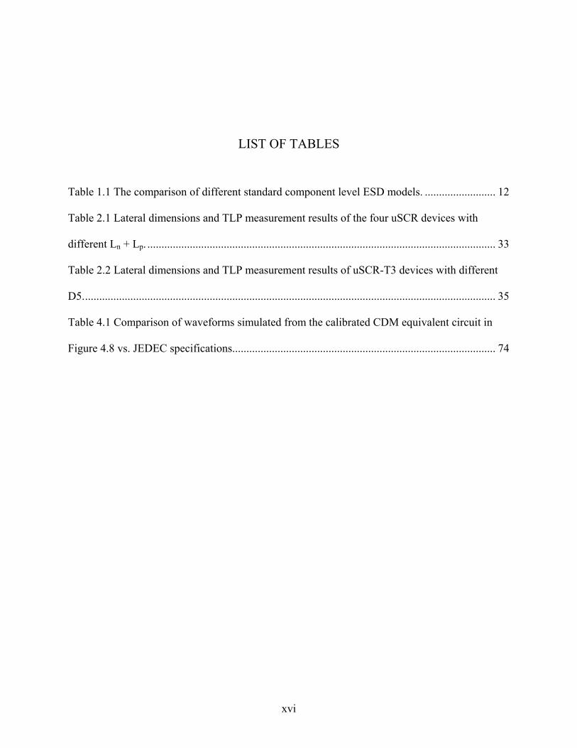
Figure 2.6 (a) Scheme of the on-chip ESD protection realized with the uSCR device. (b) Equivalent circuit schematic diagram of the layout showed in (a). It shows the discharge current loops under the different HBM and CDM zaps.
The proposed uSCR in this chapter with a trigger voltage lower than 8 V, a holding
voltage higher than 6 V, an ESD robustness higher than 60 mA/μm and an HBM as well as a
CDM ESD-protection levels as high as +/- 8 kV and +/- 2 kV, respectively, is one of the most
advanced ESD devices to date for low-voltage ESD-protection applications.
(a)
(b)
38
2.5. Chapter Summary
As technology advances, the requirement for the trigger and holding voltages of the ESD
devices becomes more stringent. This chapter starts with discussion of the triggering mechanism
of the SCR device then presents a novel low trigger-/high holding-voltage SCR devices, called
uSCR, which have been successfully designed, fabricated and characterized on a 0.35 μm
BiCMOS process. Experimental results have verified that the trigger voltage can be reduced to
less than 8 V without using any external trigger circuitry and that the holding voltage can be
increased to more than 6 V without sacrificing the ESD robustness. The ESD robustness of the
uSCR device makes it be used as an area efficient ESD protection cell in VSS-based ESD
protection scheme. The area efficiency is realized by three factors:
1. The uSCR device itself is robust, with a IT2 higher than 60 mA/μm at both
forward and reverse operation region.
2. When apply the uSCR device in VSS-based ESD protection scheme, the extra
diode for negative ESD strike can be removed, with relaying on the uSCR
device to dump the ESD current of negative strike.
3. Comparing with VDD-based ESD protection scheme, the VSS-based ESD
protection scheme dose not have to involve an ESD clamp between I/O pad and
VDD.
39
CHAPTER 3. DEVELOPMENT OF HIGH HOLDING CURRENT SCR FOR HIGH VOLTAGE ESD PROTECTION APPLICATIONS
3.1. Introduction
High voltage technologies have been developed by extending mature, less expensive
CMOS technologies (0.18 μm and above) with new features for specific automotive or consumer
electronics products, etc, which offers significant economical advantages in this competitive
market segment [76]. The new features, such as equipping the MOS transistors with thick gate
oxides and lowly doped drain/source implants to increase the voltage tolerance of the devices,
allows driving the maximum operating voltages to the limits of the process technology. The ESD
protection cells for the high voltage technologies need to be able to withstand the high voltages.
However, these new technology features will significantly degrade the high current performance
of conventional protection devices.
ESD related issues in high voltage technologies including: 1) Strong snapback. The
additional feature in high voltage technology, low doping implants, will strongly impact the
snapback behavior of conventional snapback ESD protection device, like ggNMOS. The holding
voltage of the ggNMOS for high voltage technologies are far away below operation voltage, VDD.
This is due to Kirk effect [77]-[78]. Also, the ggNMOS shows the immediate degradation after
snapback. 2) Intrinsic high voltage NMOS reliability issues due to high voltage and high current
applications. 3) Multi-finger non- uniformly triggering. The Murphy’s law always prefers to turn
on one MOSFET finger ahead of any other ones. The condition, VT1 (the trigger voltage) < VT2
40
(the thermal runaway voltage), needs to meet to make other fingers come to play together before
the first-turn-on finger fails, especially for the silicide technologies. It is hard to make VT1 < VT2
valid in high voltage technologies [79]. 4) Latchup risk. Due to the strong snapback, transient
latchup may occur due to the low holding voltage of the ESD protection cell. 5) High series
resistance, which is due to the increasing critical distance in high voltage technologies to avoid
punch through when the lightly doped diffusions make the depletion region wider. 6) The
triggering competition between the weak output driver and the parallel ESD clamp are tougher in
high voltage technologies.
We have discussed in previous chapters that the SCR device has long been used as a
robust and area-efficient on-chip ESD protection device. Its inherent regenerative feedback
mechanism leads to a deep-snapback characteristic with a relatively small holding voltage [80].
This reduces the power dissipation in the SCR during the ESD event and makes the SCR device
more robust than other ESD devices such as diodes and GGNMOS [81].
The SCR device is one of the good candidate devices to be used for high voltage ESD
protection [76]. When using SCR devices for ESD protection of high voltage ICs, the transient
trigger voltage needs to be tailored to meet high voltage application. Also, the small holding
voltage will become problematic, especially for the case of a supply clamp. The VDD is much
higher for high voltage applications than that when the technology is for CMOS low voltage
application, for example, VDD can be from 5 V to 65 V and higher. The low holding voltage
would allow the SCR to remain in its low conductive state after the ESD event dissipated if the
holding voltage is smaller than the supply voltage. And the SCR-based devices with low holding
41
voltage would interfere with the normal circuit operation when accidentally triggered on by noise
pulses, which is known as the ESD-induced latchup [49].
There are two solutions to avoid such kind of latchup. One is to increase the holding
voltage (VH) to be greater than the maximum voltage supply of VDD [82]-[83], which either has
to stack several ESD protection devices by consuming a large layout area [82] or has to sacrifice
the robustness [83] which is right the advantage of SCR-based devices due to the relatively low
holding voltage. Another solution is to increase the triggering current [68] or the holding current
of the SCR devices [69]. As shown in Figure 3.1, if the SCR device has an holding current (IH)
higher than certain latchup-immune current (ILU), the latchup due to ESD device false triggering
can be avoided during normal operation as well as under the overshooting and undershooting
noise pulses. Additionally, since the requirement of VH > VDD can be dropped, the failure current
(IT2) of the SCR device can be higher, comparing with the other latchup-immune solution which
requires VH > VDD. By doing this way, the big advantage of high failure current of the SCR
device due to deep-snapback can be utilized well. Literature [68]-[69] have reported such SCR
devices with high IH for latchup-free solutions, but both cases have to involve ground-gate MOS
devices which normally will incur serious reliability weakness issues for high voltage
technologies [76].
42
Figure 3.1 The comparison of generic characteristics of the high holding current and the high holding voltage snapback ESD protection cells within the ESD design window defined by the supply voltage (VDD), Vmax and the latchup-immune current (ILU).
In this chapter, we will present a new high holding current SCR (HHC-SCR) device with
a holding current as high as 24 mA/μm and a high failure current, IT2, for high voltage
applications without involving any external circuitry or extra devices. The avalanche
multiplication factor (M) and the current gains of PNP and NPN bipolar transistors coupled in
SCR devices are two factors to determine the holding current of SCR devices. The SCR device
presented in this paper perform a high holding current by realizing an optimized balance between
current gains and M.
ESD Design Window
Normal Operation
Inte
rnal
Circ
uitry
Bre
akdo
wn
VT
IT
IH
IT2
VH
VDD Vmax
Voltage
Cur
rent
ILU
VH IH
VT
IT
IT2
Latchup Immunity Solutions VH > VDD IH > ILU
43
3.2. Holding Current of SCR Devices
Figure 3.2 shows the cross-section view of a conventional triple-well SCR structure.
There is no local oxidation of silicon (LOCOS) between the N+ region under terminal N-Well
and the P+ region under terminal.Emitter_PNP. Also, there is no LOCOS between the N+ region
under terminal.Emitter_NPN and the P+ region under terminal P-Well. It is well known such
SCR device is a PNP-NPN coupled system and triggered by the avalanche breakdown of the
base-collector junction which is N-Extension/P-Well junction in Figure 3.2. The avalanche
current going through the both substrate resistances, RN-Well and RP-Well, will raise the base-
emitter biases of the PNP and NPN transistors to turn on both bipolar transistors in the end. Then
the SCR device is triggered and enter conduction mode. The high avalanche breakdown voltage
of the N-Extension/ P-Well junction ensures the SCR device to be triggered higher than 45 V for
Figure 3.2 The device cross-section view of the conventional SCR structure.
44
The SCR device physics before triggering has been discussed in detail in Chapter 2.Here
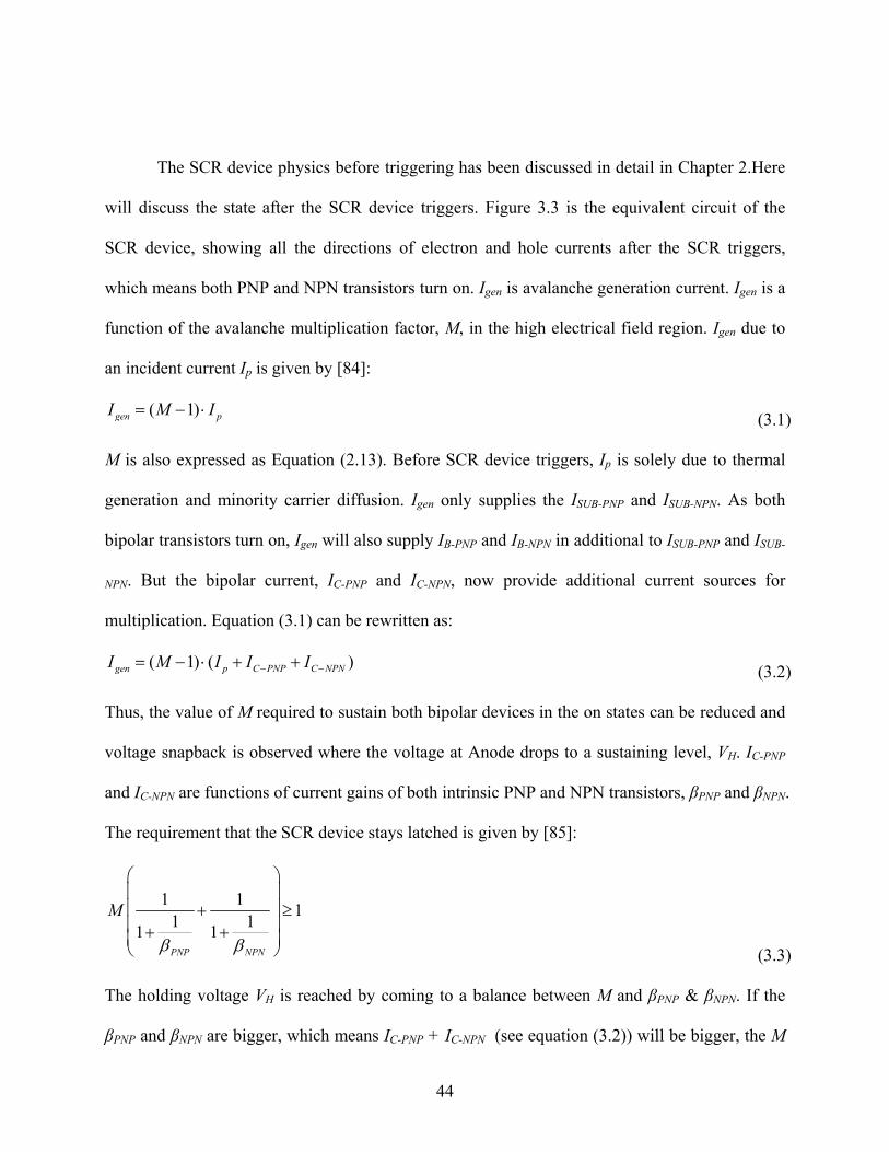
will discuss the state after the SCR device triggers. Figure 3.3 is the equivalent circuit of the
SCR device, showing all the directions of electron and hole currents after the SCR triggers,
which means both PNP and NPN transistors turn on. Igen is avalanche generation current. Igen is a
function of the avalanche multiplication factor, M, in the high electrical field region. Igen due to
an incident current Ip is given by [84]:
( 1)gen pI M I= − ⋅ (3.1)
M is also expressed as Equation (2.13). Before SCR device triggers, Ip is solely due to thermal
generation and minority carrier diffusion. Igen only supplies the ISUB-PNP and ISUB-NPN. As both
bipolar transistors turn on, Igen will also supply IB-PNP and IB-NPN in additional to ISUB-PNP and ISUB-
NPN. But the bipolar current, IC-PNP and IC-NPN, now provide additional current sources for
multiplication. Equation (3.1) can be rewritten as:
( 1) ( )gen p C PNP C NPNI M I I I− −= − ⋅ + + (3.2)
Thus, the value of M required to sustain both bipolar devices in the on states can be reduced and
voltage snapback is observed where the voltage at Anode drops to a sustaining level, VH. IC-PNP
and IC-NPN are functions of current gains of both intrinsic PNP and NPN transistors, βPNP and βNPN.
The requirement that the SCR device stays latched is given by [85]:
1 1 11 11 1PNP NPN
M
β β
⎛ ⎞⎜ ⎟⎜ ⎟+ ≥⎜ ⎟+ +⎜ ⎟⎝ ⎠ (3.3)
The holding voltage VH is reached by coming to a balance between M and βPNP & βNPN. If the
βPNP and βNPN are bigger, which means IC-PNP + IC-NPN (see equation (3.2)) will be bigger, the M
45
will be less resulting a smaller VH, vice versa. The corresponding current when the SCR device
reaches VH is the holding current, IH, which can be expressed as (as shown in Figure 3.3):
H SUB PNP E PNPI I I− −= + (3.4)
SUB PNP gen C NPN B PNPI I I I− − −= + − (3.5)
Since the Ip is much smaller comparing with IC-PNP and IC-NPN after the device turns on, we can
get the relationship:
( 1) ( )gen C PNP C NPN genI M I I I− −≈ − ⋅ + = (3.6)
C PNPE PNP
PNP
IIα
−− =
(3.7)
C PNPB PNP
PNP
IIβ−
− = (3.8)
By replacing (3.6), (3.7), (3.8) and (3.9) in (3.5), we finally have:
( )H C PNP C NPNI M I I− −= ⋅ + (3.9)
As the aforementioned, an increasing of IC-PNP+IC-NPN will normally cause M decreasing.
So the high holding current will be realized by designing a SCR structure with a maximal M(IC-
PNP+IC-NPN), which means to find an optimized combination of M and βPNP & βNPN.
46
Cathode
Anode
RP-Well
PNP
NPN
Injection
Injection
Generation
Generation
Hole CurrentElectron Current
IE-PNP
IE-NPN
IC-NPNIB-NPN
IC-PNP
ISUB-NPN
RN-Well
ISUB-PNP
IB-PNPIgen
IHVH
RP
IH Cathode
Anode
RP-Well
PNP
NPN
Injection
Injection
Generation
Generation
Hole CurrentElectron Current
IE-PNP
IE-NPN
IC-NPNIB-NPN
IC-PNP
ISUB-NPN
RN-Well
ISUB-PNP
IB-PNPIgen
IHVH
RP
IH
Figure 3.3 The equivalent circuit of the SCR device, showing the directions of all electron and hole current components after the both PNP and NPN transistors turn on.
3.3. Device Structure, Experimental Results and Discussions
The top view of the proposed HHC-SCR device is shown in Figure 3.4(b). Figure 3.4(a)
is the top topology of the conventional SCR device, corresponding to the cross section view in
Figure 3.2. Its well tie and emitter tie for both PNP and NPN transistors are strips. Both devices
shown in Figure 3.4(a) and (b) have D3=D4=8 micron and D1=D2=D5=D6= 1.6 micron. In
order to realize high holding current, we have to increase the βPNP & βNPN while without
decreasing M that much. Comparing with the conventional SCR device (Figure 3.4 (a)), the
47
proposed HHC-SCR device gets rid of the strips of N-Well tie and P-Well tie and insert the well
ties into the strips of emitter ties of both PNP and NPN transistors, realizing a pattern of
intermittent well tie and emitter tie. By doing this, the lengths of base region of both transistors
are reduced, which will result in the increased βPNP & βNPN. Also, the intermittent pattern reduced
the effective emitter areas of both transistors such that the emitter injection efficiencies are
decreased. The impact ionization has to be more intensive to get enough Igen, which will incur a
higher M and higher holding voltage, VH.
P+
N+
P+
N+
P+
N+
P+
N+
P+
N+
P+
N+
P+
N+
P+
N+
N+
P+
P+
N+
P+
N+
P+
N+
P+
N+
P+
N+
P+
N+
P+
N+
N+
P+
D2 D3 D4 D5
N-E
x ten
s ion
P-W
ell
P+
N+
P+
N+
P+
P+
N+
P+
P+
N+
P+
P+
N+
N+
P+
P+
N+
N+
P+
N+
N+
P+
N+
N+
P+
N+
N+
P+
D2 D3 D4 D5
N-E
x ten
sion
P-W
ell
P+
N+
P+
N+
P+
P+
N+
P+
N+
P+
P+
N+
P+
N+
N+
P+
P+
N+
N+
P+
N+
P+
N+
N+
P+
N+
P+
N+
N+
P+
D2 D3 D4 D5
N-E
x ten
sion
P-W
ell
N+
N+
N+
N+
N+
N+
N+
N+
N+
N+
N+
N+
N+
N+
N+
N+
N+
P+
P+
P+
P+
P+
P+
P+
P+
P+
P+
P+
P+
P+
P+
P+
P+
P+
D1 D2 D3 D6D4 D5
N-E
xten
sion
P -W
ell
P+
P+
P+
P+
P+
P+
P+
P+
P+
P+
P+
P+
P+
P+
P+
P+
P+
N+
N+
N+
N+
N+
N+
N+
N+
N+
N+
N+
N+
N+
N+
N+
N+
N+
P+
N+
P+
N+
P+
N+
P+
N+
P+
N+
P+
N+
P+
N+
P+
N+
N+
P+
P+
N+
P+
N+
P+
N+
P+
N+
P+
N+
P+
N+
P+
N+
N+
P+
D2 D3 D4 D5
N-E
x ten
s ion
P-W
ell
P+
N+
P+
N+
P+
P+
N+
P+
P+
N+
P+
P+
N+
N+
P+
P+
N+
N+
P+
N+
N+
P+
N+
N+
P+
N+
N+
P+
D2 D3 D4 D5
N-E
x ten
sion
P-W
ell
P+
N+
P+
N+
P+
P+
N+
P+
N+
P+
P+
N+
P+
N+
N+
P+
P+
N+
N+
P+
N+
P+
N+
N+
P+
N+
P+
N+
N+
P+
D2 D3 D4 D5
N-E
x ten
sion
P-W
ell
N+
N+
N+
N+
N+
N+
N+
N+
N+
N+
N+
N+
N+
N+
N+
N+
N+
P+
P+
P+
P+
P+
P+
P+
P+
P+
P+
P+
P+
P+
P+
P+
P+
P+
D1 D2 D3 D6D4 D5
N-E
xten
sion
P -W
ell
P+
P+
P+
P+
P+
P+
P+
P+
P+
P+
P+
P+
P+
P+
P+
P+
P+
N+
N+
N+
N+
N+
N+
N+
N+
N+
N+
N+
N+
N+
N+
N+
N+
N+
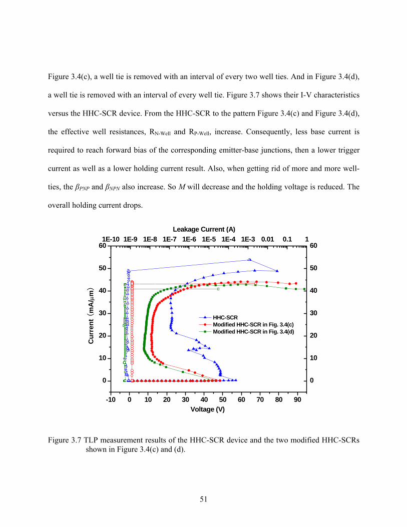
Figure 3.4 The top view of the SCR devices. (a) Strip topology of conventional SCR, (b) segmented topology of high holding current SCR (HHC-SCR), (c) modified HHC-SCR with a well tie removed from each strip with an interval of every two well ties, and (d) modified HHC-SCR with a well tie removed from each strip with an interval of every well tie.
(b) (c) (d) (a)
48
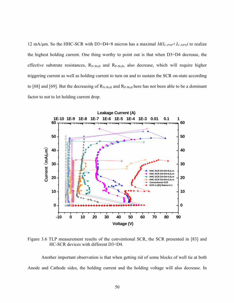
Figure 3.6. shows the TLP I-V characteristic of the proposed HHC-SCR as well as the
conventional SCR device and the SCR device reported in [83] with the segment ratio of 1:1. Test
devices were fabricated on the BiCMOS 0.6 μm process and all have a total width of 100 μm.
Figure 3.5 illustrates the segmented topology of the device in [83] for comparison. The device
shown in Figure 3.5 also has D3=D4=8 micron and D1=D2=D5=D6=1.6 micron. The
conventional SCR device triggers at 45 V. Its holding voltage is very low at 5.5 V which give the
device the high IT2 which is higher than 50 mA/μm. From the conventional SCR to the SCR
device in [83], the injection efficiency has been reduced significantly, so IC-PNP + IC-NPN has been
reduced a lot while M has to increase significantly to maintain an enough Igen. As a compensation
result, IH of the SCR device in [83] doesn’t change a lot but a high holding voltage of 45 V is
reached. Comparing with the SCR device in [83], the proposed HHC-SCR keeps the same
injection efficiency but has a higher βPNP and βNPN, which will give a higher IC-PNP + IC-NPN,
which causes M dropping a little to realize a maximal M(IC-PNP+IC-NPN), which means the best
combination of M and βPNP & βNPN to realize the highest high holding current (refer to Equation
(3.9)). The HHC-SCR device has performed a holding current as high as 24 mA/ μm, which can
effectively avoid latch-up without having to increase the holding voltage higher than the
maximum supply voltage when using a such device for ESD protection applications. Such a high
holding current is much higher than those having been reported in [68] and [69]. The leakage
current of the HHC-SCR device is at nA range and the turn-on resistance is pretty low. In
additional, with a lower M, the HHC-SCR device has a lower holding voltage, 22 V, which gives
a higher ESD robustness comparing with the device in [83]. The IT2 of HHC-SCR is 48.8 mA/μm
49
versus 28 mA/μm in [83] which relies on increasing VH to be higher than VDD to realize the
latchup immunity. And the IT2 of HHC-SCR is almost as good as that of the conventional SCR.
N+
N+
N+
N+
N+
N+
N+
N+
N+
N+
N+
N+
N+
N+
N+
N+
N+
P+
P+
P+
P+
P+
P+
P+
P+
P+
P+
P+
P+
P+
P+
P+
P+
P+
P+
N+
P+
N+
P+
N+
P+
N+
P+
N+
P+
N+
P+
N+
P+
N+
N+
P+
D1
P+
N+
P+
N+
P+
N+
P+
N+
P+
N+
P+
N+
P+
N+
N+
P+
D2 D3 D6D4 D5
N-E
xten
sion
P-W
ell
N+
N+
N+
N+
N+
N+
N+
N+
N+
N+
N+
N+
N+
N+
N+
N+
N+
P+
P+
P+
P+
P+
P+
P+
P+
P+
P+
P+
P+
P+
P+
P+
P+
P+
P+
N+
P+
N+
P+
N+
P+
N+
P+
N+
P+
N+
P+
N+
P+
N+
N+
P+
D1
P+
N+
P+
N+
P+
N+
P+
N+
P+
N+
P+
N+
P+
N+
N+
P+
D2 D3 D6D4 D5
N-E
xten
sion
P-W
ell
Figure 3.5 The illustration of the segment topology of the SCR device reported in reference [83].
The further increasing of βPNP and βNPN are also performed to verify the maximal M(IC-
PNP+IC-NPN) has been reached. Taking the proposed HHC-SCR in Figure 3.4(b) as a benchmark,
which has a D3=D4=8 micron, D3=D4 is reduced from 8.0 micro to 2.0 micron, which cause
βPNP and βNPN increasing. Figure 3.6 shows the TLP measurement results of HHC-SCR with
different D3 and D4. It can be seen that when D3=D4 decrease, the lengths of base region of
both transistors are reduced, which will result in the increased βPNP & βNPN then the increased IC-
PNP + IC-NPN. However, the holding voltage decreases since M has decreased. As the result, the
overall holding current, which is the product of M and IC-PNP + IC-NPN, drops from 24 mA/μm to
50
12 mA/μm. So the HHC-SCR with D3=D4=8 micron has a maximal M(IC-PNP+IC-NPN) to realize
the highest holding current. One thing worthy to point out is that when D3=D4 decrease, the
effective substrate resistances, RN-Well and RP-Well, also decrease, which will require higher
triggering current as well as holding current to turn on and to sustain the SCR on-state according
to [68] and [69]. But the decreasing of RN-Well and RP-Well here has not been able to be a dominant
Itfp and Itrp are the parasitic forward and reverse transport currents, WSP is the portion of Iccp from
Vbep, ISP is parasitic saturation current, NFP is parasitic forward emission coefficient, Qbp is
parasitic normalized base charge, and IKP is parasitic knee current. It can be seen that Qbp only
includes high-level forward injection, not including the early effects and high-level reverse
injection. However, the parasitic PNP in Zhou et al.’s model is working in reverse active mode
which the parasitic model doesn’t model. So the model can not fit the measurement data in
positive operation very well.
The configuration of Zhou et al.’s maromodel doesn’t have efficient current path to
describe the device characteristic in negative operation. That’s why the negative characteristic is
far away from the measurement data. Also, the simulation results show the major portion of the
negative current comes from the impact ionization of source-to-bulk junction of the NMOS
transistor built in the macromodel, not coming from the forward biased diode.
Figure 4.5(a) and (b) compare the measured and simulated transient responses of the TLP
voltage and current, respectively, in the SCR right after triggering point. The pad voltage reaches
a peak value of 9.42 V and then is decreased to 5.11 V (holding voltage) before it is turned off.
The pad current, on the other hand, reaches a maximum value of 218 mA after the device turns
on.
70
-6 -4 -2 0 2 4 6 8 10 12
-1.5
-1.0
-0.5
0.0
0.5
1.0
1.5
Pad
Cur
rent
(A)
Pad Voltage (V)
New Model TLP Measurement Model by Zhou et. al.
Figure 4.4 Simulated and measured TLP I-V characteristics of the HH-LVTSCR.
Figure 4.6 shows the simulation results of the transient response of the pad voltage using
the presented SCR macromodel under very-fast TLP (VFTLP) condition with a rise-time of 250
ps at a current level of 1A. The waveform demonstrates a significant voltage overshoot at the
beginning of the pulse.
71
67.15 67.20 67.25 67.30 67.35
02468
10
67.15 67.20 67.25 67.30 67.35
0.000.050.100.150.200.25
(b)
(a)
Volta
ge (V
)
Time (μs)
C
urre
nt (A
)
Simulation Measurement
Figure 4.5 (a) Simulated and measured time-dependent pad voltages and (b) simulated and measured pad currents right after the SCR triggering.
0 1 2 3 4 5 6 7
0
5
10
15
20
Volta
ge (V
)
Time (ns)
Figure 4.6 The simulated pad voltage under VFTLP pulse at a steady-state current of 1A.
72
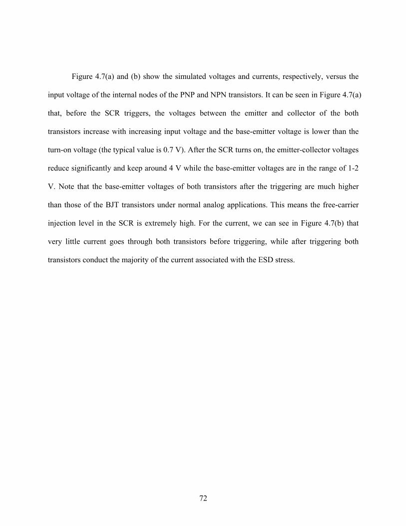
Figure 4.7(a) and (b) show the simulated voltages and currents, respectively, versus the
input voltage of the internal nodes of the PNP and NPN transistors. It can be seen in Figure 4.7(a)
that, before the SCR triggers, the voltages between the emitter and collector of the both
transistors increase with increasing input voltage and the base-emitter voltage is lower than the
turn-on voltage (the typical value is 0.7 V). After the SCR turns on, the emitter-collector voltages
reduce significantly and keep around 4 V while the base-emitter voltages are in the range of 1-2
V. Note that the base-emitter voltages of both transistors after the triggering are much higher
than those of the BJT transistors under normal analog applications. This means the free-carrier
injection level in the SCR is extremely high. For the current, we can see in Figure 4.7(b) that
very little current goes through both transistors before triggering, while after triggering both
transistors conduct the majority of the current associated with the ESD stress.
73
0 5 10 15 20-0.8
-0.6
-0.4
-0.2
0.0
0.2
0.4
0.6
0.8
0 5 10 15 20
0
2
4
6
8
10
12
(b)
(a)
Cur
rent
(A)
Anode to Cathode Voltage (V)
NPN-IB NPN-IC NPN-IE PNP-IB PNP-IC PNP-IE
Volta
ge (V
)
Anode to Cathode Voltage (V)
NPN-Vbe
NPN-Vce
PNP-Veb
PNP-Vec
Figure 4.7 Simulated (a) base-emitter and collector-emitter voltages of the PNP and NPN transistors and (b) emitter, base and collector currents of the PNP and NPN transistors.
4.4. CDM Transient Simulation of I/O Circuit
4.4.1. CDM Pulse Circuit
The CDM event can be emulated using the equivalent circuit in Figure 4.8 consisting of a
capacitance, inductance, resistance, and a JEDEC-specified small target made of a piece of metal
with a resistance of about 45 ohm. The current waveform associated with the CDM discharge
process depends on the values of the RLC and the charging voltage. In order to comply with the
74
JEDEC standard [24]-[25], we have calibrated the RLC values, as shown in Figure 4.8, and the
simulated waveforms of two CDM voltages (500 and 1000 V) compare with the JEDEC specs
listed in Table 4.1. The calibrated equivalent circuit in Figure 4.8 will be used to generate CDM
Figure 4.8 Current waveforms of CDM pulses generated by the calibrated CDM equivalent circuit (insert) with the small target.
Table 4.1 Comparison of waveforms simulated from the calibrated CDM equivalent circuit in Figure 4.8 vs. JEDEC specifications.
0.86< 25%Ip0.42< 25%IpU+Overshoot (A)
-2.9< 50%Ip-1.5< 50%IpU-Undershoot (A)
0.8971.0±0.50.8881.0±0.5TdFull width at half height (ns)
335.1< 400341.08< 400trRise time (ps)
10.3611.5 (±15%)5.25.75 (±15%)IpPeak current Magnitude (A)
SimulationJEDEC Spec.SimulationJEDEC Spec.
1 kV500 VTest voltage (V)
Small Target
75
4.4.2. Experimental Results
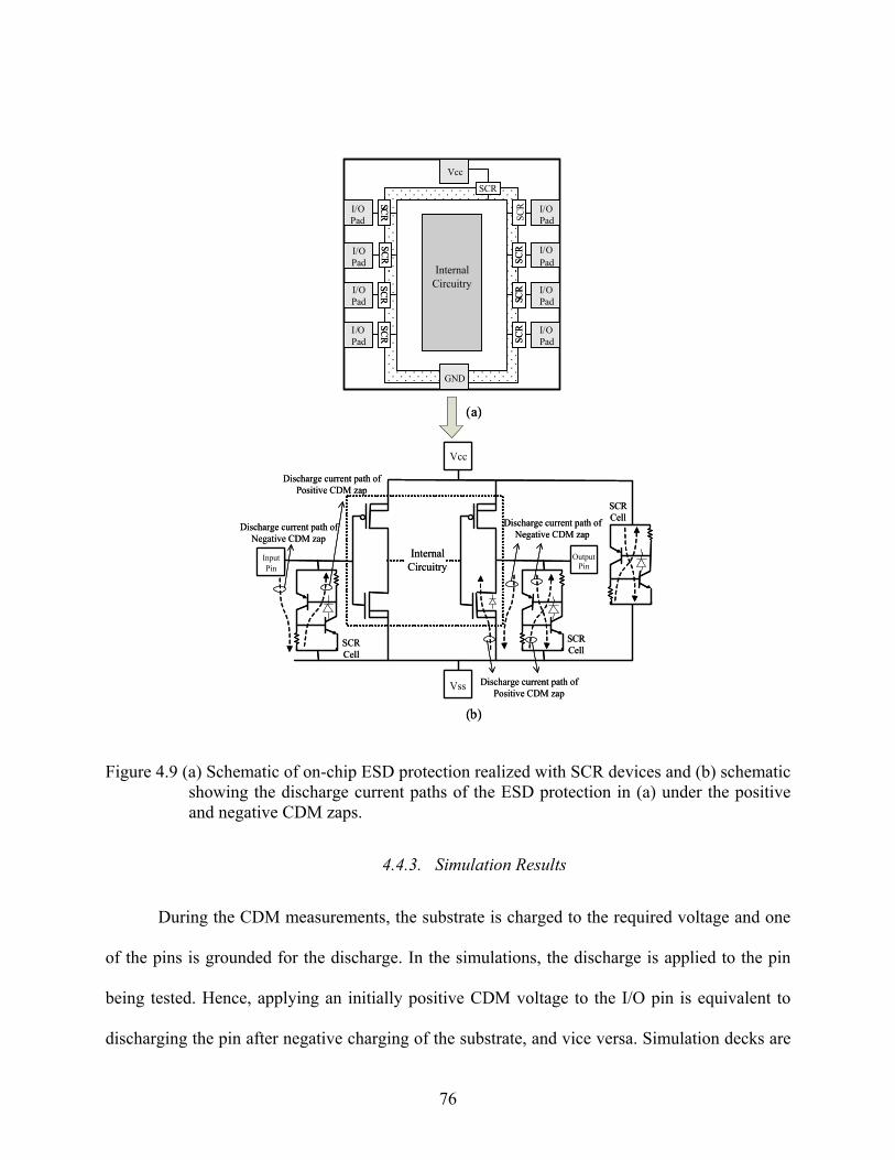
The HH-LVTSCR devices with a width of 100 micron were integrated into a single pole
double throw (SPDT) analog switch. Figure 4.9(a) shows its on-chip ESD protection scheme.
The anode terminals of the SCR devices are all connected to the pads and their cathode terminals
are all connected to the common ground bus of the chip. The die size of the test chip is 1000*800
μm2, and its package type is 10-lead MicroPAK.
Figure 4.9(b) is the equivalent circuit schematic diagram of the layout showed in (a). In
the SPDT analog switch, there are three types of pins: input-only pins, output-only pins and
power supply pins. The ESD protection is provided by the SCR devices conducting current from
pins to ground bus, which is VSS-based ESD protection scheme as shown in Figure 1.8. Figure
4.9(b) illustrates the discharging paths under the JEDEC-standard CDM zaps. The diode inside
each SCR cell and the output NMOS denotes the device when it is working in the negative
operation.
SPDT analog switch parts are stressed by Thermo KeyTek RCDM automatic tester from
250 V to 1 kV. The stress method is compliance with JEDEC standard [24]-[25]. Those parts are
screened for pin leakage and functionality by automatic test equipment (ATE) before and after
CDM zaps to identify the failure voltage level. The test results revealed that, with the SCR
protecting devices at the pin, the input pins will fail after 500 V CDM zap and the SCR devices
can protect output pins up to 1 kV CDM.
76
SCR
SCR
Internal Circuitry
SCR
SCR
S CRSCR
SCRS CR
I/O Pad
I/O Pad
I/O Pad
I/O Pad
Vcc
GND
Internal Circuitry
Input Pin
OutputPin
Vcc
Vss
SCR Cell
SCR Cell
SCR Cell
Discharge current path ofPositive CDM zap
SCR
I/O Pad
I/O Pad
I/O Pad
I/O Pad
Discharge current path ofNegative CDM zap
Discharge current path ofNegative CDM zap
Discharge current path ofPositive CDM zap
(a)
(b)
SCR
SCR
SCR
Internal Circuitry
SCR
SCR
SCR
SCR
S CRS CR
SCRSCR
SCRSCR
S CRS CR
I/O Pad
I/O Pad
I/O Pad
I/O Pad
Vcc
GND
Internal Circuitry
Input Pin
OutputPin
Vcc
Vss
SCR Cell
SCR Cell
SCR Cell
Discharge current path ofPositive CDM zap
SCR
I/O Pad
I/O Pad
I/O Pad
I/O Pad
Discharge current path ofNegative CDM zap
Discharge current path ofNegative CDM zap
Discharge current path ofPositive CDM zap
(a)
(b)
Figure 4.9 (a) Schematic of on-chip ESD protection realized with SCR devices and (b) schematic showing the discharge current paths of the ESD protection in (a) under the positive and negative CDM zaps.
4.4.3. Simulation Results
During the CDM measurements, the substrate is charged to the required voltage and one
of the pins is grounded for the discharge. In the simulations, the discharge is applied to the pin
being tested. Hence, applying an initially positive CDM voltage to the I/O pin is equivalent to
discharging the pin after negative charging of the substrate, and vice versa. Simulation decks are
77
created to simulate the response of the input-only and output-only pins under CDM stresses. The
macromodel developed is used to model the SCR devices and the standard BSIM3v3 model is
used to model the MOS transistors in the core circuit. The NMOS in output buffer for pull-down
has the snapback modeling capability.
Figure 4.10 shows the simulated transient voltage and current characteristics of the input-
only pin subjecting to a positive 500 V CDM stress (i.e., negative substrate charging). The
maximum voltage at the input pad, which is also the maximum voltage stressed on the gate oxide
of the input MOS, is as high as 35 V. Even though the oxide breakdown voltage for a 1-ns rise
time CDM pulse is much higher than that for a dc stress [95], but the 35 V resulted from the
CDM is very likely to be sufficiently large to damage the core circuit. The ATE testing showed
the leakage current of the input pins increases significantly after the 500 V CDM stress,
indicating the gate oxide of the input MOS has failed. This may stems from that fact that the HH-
LVTCSR doesn’t trigger fast enough to discharge the CDM stress current, as evidenced by the
current waveform lagging the voltage waveform during the positive portion of the first cycle.
The simulation results shown in Figure 4.6 also show the voltage overshoot. Ideally, if the SCR’s
turn-on time is sufficiently fast, the maximum input pad voltage is the same as the SCR trigger
voltage of 9.4 V. But in practice, the slow SCR turn-on leads to a voltage build up of about 35 V
until the SCR can start to conduct a large current. In the negative portion of the first cycle, the
maximum voltage is much lower because the current will discharge through the forward-biased
P-Substrate/N-Well and P-Well/N-Well junction diodes. The diodes can turn on quickly enough
to safely shunt the current. During the second cycle, the HH-LVTSCR follows the voltage
Figure 4.11 Simulated transient voltage and currents at the output-only pin under a positive 1 kV CDM stress.
The above simulation finding is consistent with the testing results that the input pins
failed after a 500 V CDM stress and the output pins failed at a higher level of 1 kV CDM. While
the output NMOS is self-protecting, the ESD protection device, like HH-LVTSCR considered, is
still indispensable for the output pins. The total width of the output NMOS is not big enough to
handle all the ESD current (the total width of the output NMOS in this presented case is 40 μm)
and its area efficiency of ESD protection is lower than that of the SCR protection device.
80
In order to improve the CDM robustness of the pins, a clear way is to reduce the pad
clamping voltage. A suggested way is to provide an alternate discharge path from pad to VSS or
to reduce the impedance of the existing path [104] or to design new ESD protection structures
which can trigger fast enough to offer adequate CDM protection.
Thus, the model developed, together with the knowledge of pad voltage that can be
applied to the I/O pin without damaging the core circuit, can be used to predict the I/O pin ESD
protection level offered by the SCR protection devices.
4.5. Chapter Summary
In this chapter, we have presented a comprehensive compact model of SCR for the
simulation of integrated circuits subjected to a pervasive ESD event called the charge device
model (CDM). The work illustrated the useful and effective macromodeling approach of
integrating the various industry standard models to describe the individual devices imbedded in
the SCR. In addition, the modeling of the avalanche current sources, substrate parastics, and
capacitances were discussed. The issue of parameter extraction was addressed as well. The
macromodel has been implemented into Cadence SPICE, and TLP and transient simulations
have been carried out. A 0.35-μm CMOS circuit subjecting to CDM stresses was also considered
and tested in support of the modeling development.
81
CHAPTER 5. COMPARISON OF VBIC AND CONVENTIONAL GUMMEL-POON MODEL FOR ESD SCR COMPACT MODELING
5.1. Introduction
In Chapter 4, we have already discussed how important to build a predictable compact
model for SCR devices for ESD protection design and what are the difficulties of building such
model. Also, Chapter 4 presents a marcomodeling approach to build an accurate, stable and fast
SCR compact model by taking the advantage of the advanced BJT model, VBIC. This modeling
approach offers simplicity, wide availability and compatibility with most commercial simulators.
In additional, this approach by using VBIC model can quickly adapted to technology scaling
when new physical phenomena is updated into standard VBIC model for the latest state-of-art
technologies by compact modeling community. Furthermore, the sophisticated capacitance
modeling and the parasitical PNP in the advanced VBIC model ensure this macromodel
approach can simulate the response of the SCR device to very fast transient stimulus such as
CDM.
The macromodeling approach is to use the existing device model to build an equivalent
sub-circuit to describe the characteristic of the device to be modeled. This approach is highly
suitable for modeling a device whose behavior is hard to describe with a close-form analytical
solutions. The SCR device is a PNP-NPN transistor coupled system. The straightforward idea to
model this device is to consolidate a PNP and a NPN BJT to represent the SCR device. The
question is what kind of model should be used for the PNP and NPN transistors in SCR sub-
82
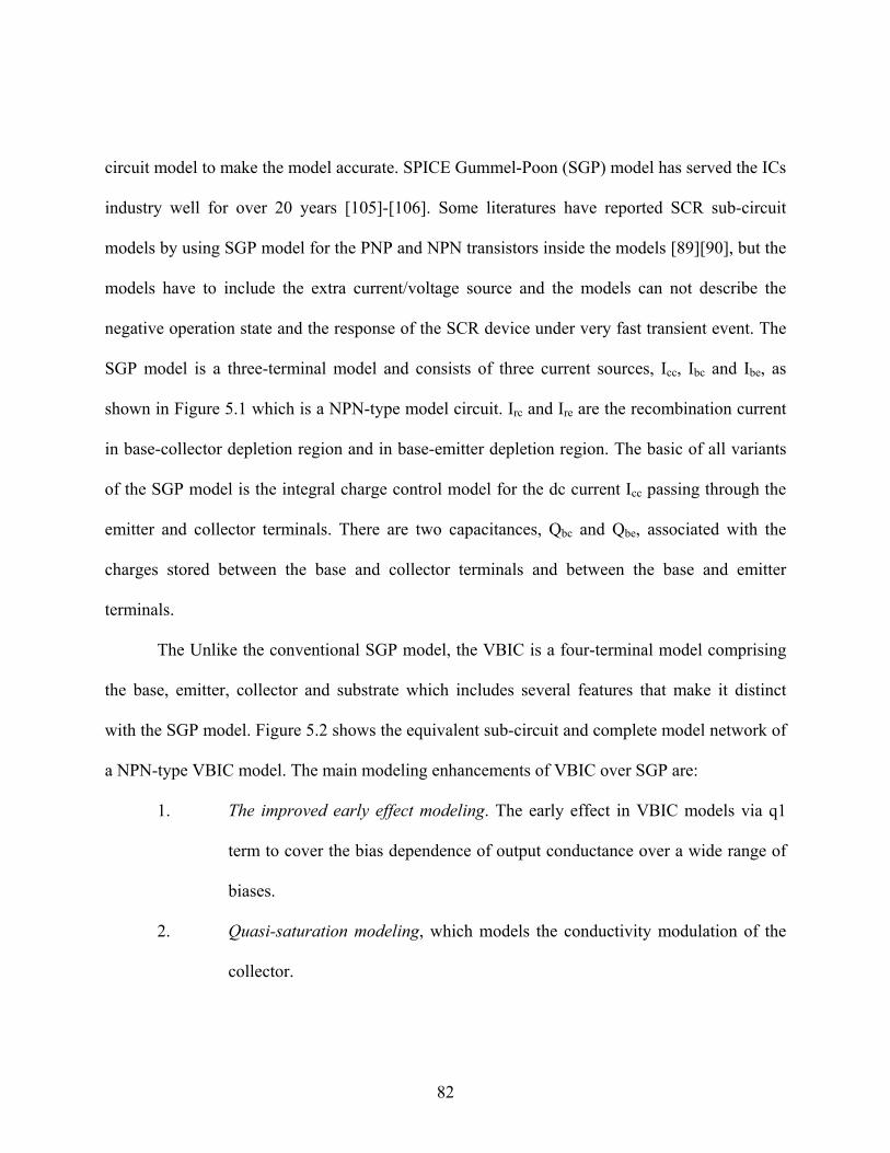
circuit model to make the model accurate. SPICE Gummel-Poon (SGP) model has served the ICs
industry well for over 20 years [105]-[106]. Some literatures have reported SCR sub-circuit
models by using SGP model for the PNP and NPN transistors inside the models [89][90], but the
models have to include the extra current/voltage source and the models can not describe the
negative operation state and the response of the SCR device under very fast transient event. The
SGP model is a three-terminal model and consists of three current sources, Icc, Ibc and Ibe, as
shown in Figure 5.1 which is a NPN-type model circuit. Irc and Ire are the recombination current
in base-collector depletion region and in base-emitter depletion region. The basic of all variants
of the SGP model is the integral charge control model for the dc current Icc passing through the
emitter and collector terminals. There are two capacitances, Qbc and Qbe, associated with the
charges stored between the base and collector terminals and between the base and emitter
terminals.
The Unlike the conventional SGP model, the VBIC is a four-terminal model comprising
the base, emitter, collector and substrate which includes several features that make it distinct
with the SGP model. Figure 5.2 shows the equivalent sub-circuit and complete model network of
a NPN-type VBIC model. The main modeling enhancements of VBIC over SGP are:
1. The improved early effect modeling. The early effect in VBIC models via q1
term to cover the bias dependence of output conductance over a wide range of
biases.
2. Quasi-saturation modeling, which models the conductivity modulation of the
collector.
83
3. Parasitic substrate transistor modeling. VBIC model composes a intrinsic
NPN transistor and a parasitic PNP transistor.
4. Parasitic oxide capacitance modeling.
5. Avalanche current modeling. VBIC models the base-collector avalanche
current at high reverse bias when the device is in forward-active mode.
6. Decoupling of base and collector current. In the conventional SGP model, the
base and collector currents are correlated with current gain while in VBIC
model, there is no such direct connection between the two currents.
7. Improved temperature dependence modeling.
8. Self heating modeling.
9. Capacitance continuous modeling.
For ESD compact modeling purpose, are all the above advanced features benefit the sub-
circuit model with using VBIC model to be a superior one and how these distinct features benefit
the SCR compact model for ESD application? This chapter seeks to compare the difference of
SCR compact model built by using VBIC and conventional SGP in order to point out the
important features of VBIC model for building an accurate and easy-CAD implement SCR
model and explain why from device physics and model theory perspectives. First, the
development of SCR macromodels by using VBIC and SGP will be presented. The results
calculated from the VBIC-based macromodel, calculated from SGP based macromodel and
obtained from measurements will be compared. This will be followed by the discussion of what
kind of unique features in VBIC model, comparing with SGP model, make the VBIC-based
macromodel model SCR triggering and characteristics in conduction mode accurately.
84
Rb
Qbe
Qbc
Re
Rc
Icc
Ibc
Ibe Ire
Irc
B
C
E
Rb
Qbe
Qbc
Re
Rc
Icc
Ibc
Ibe Ire
Irc
B
C
E
Figure 5.1 The model circuit of the SPICE Gummel-Poon bipolar transistor model.
Re
Rci
RCX
RBX
Qbcp
Qbep
Ibc
Ibe
Iavc
IccQbc
Qbcx
Rs
Qbe
Iccp
Ibep
Ibcp
si
QbexIbex
bp
bx bi
ci
ei
cx
B
C
E
S
CS
E
Intrinsic NPN
Parasitic PNP
Excess Phase Network
Thermal Network
Itzf
IthRTH CTH
Qcxf
Flxf
t
xf1 xf2
Equivalent Sub-Circuit
bib
RBIR =Q
1Ω
bpbp
RBPR =Q
(a) (b)
B
Re
Rci
RCX
RBX
Qbcp
Qbep
Ibc
Ibe
Iavc
IccQbc
Qbcx
Rs
Qbe
Iccp
Ibep
Ibcp
si
QbexIbex
bp
bx bi
ci
ei
cx
B
C
E
S
CS
E
Intrinsic NPN
Parasitic PNP
Excess Phase Network
Thermal Network
Itzf
IthRTH CTH
Qcxf
Flxf
t
xf1 xf2
Equivalent Sub-Circuit
bib
RBIR =Q
1Ω
bpbp
RBPR =Q
(a) (b)
B
Figure 5.2 (a) The equivalent sub-circuit of VBIC bipolar transistor model and (b) the model circuit network.
85
5.2. Model Development by Using VBIC and SGP
A comprehensive SCR compact model for CDM ESD circuit simulation by using VBIC
has been developed in Chapter 4. The HH-LVTSCR has been considered to illustrate the model
development. Here we redraw Figure 4.1 as Figure 5.3 for comparison. The cross-section view
and the terminal connection in ESD bias condition of the device are shown in Figure 5.3(a) and
the sub-circuit of SCR macromodel is shown in Figure 5.3(b). The NPN bipolar transistor is
using the VBIC model which includes a built-in parasitic PNP to model the substrate parasitics.
The PNP BJT and NMOS are described by the SGP and BSIM3v3 models respectively. The
schematic of the macromodel is illustrating in Figure 4.2, showing the detailed connections of all
internal nodes.
Using this macromodel as a benchmark, another macromodel based on SGP is developed.
As shown in Figure 5.4, the NPN BJT is now described with SGP model. The rest sub-circuit of
the macromodel keeps the same in order to compare the performance of the macromodel when
using VBIC and SGP to describe the NPN transistor. The Figure 5.5 shows the detailed internal
nodes connection of the SGP-based macromodel.
Industry standard software tool IC-CAP is used for the parameter extraction. The model
extraction follows the methods presented in Section 4.2.8. The terminals, N-Well, Emitter-NPN,
P-Well and Substrate, are biased to extract the NPN VBIC model for VBIC-based macromodel
while also used to extract the NPN SGP model for SGP-based one. The model extraction of NPN
SGP also follows the standard strategies in IC-CAP user manual [101]. The rest model elements
of both macromodels are using the same extracted model parameters.
86
N - Well
P - Substrate
N - Epi
N-Well Gate
P - Well
Anode Cathode
Drain
N + P +
Substrate
RP-Well
Rsub
R N-Well-1
VBIC-NPNSGP-PNP
Dsub
P-Well
N + N + P + P +
Emitter-PNP Emitter-NPN
RN-Well-2
Parasitic-PNP
P1
P3
P2
PBL
Cathode
Anode
RN-Well -1
RP-Well
SGP-PNP
Parasitic-PNP
NMOSVBIC-NPN
RN-Well-2
Rsub
Dsub
GND
Pad
(a) (b)
Figure 5.3 (a) Cross-section view of the HH-LVTSCR and (b) equivalent circuit of the HH-LVTSCR when the macromodel is using VBIC model to describe the NPN transistor.
N - Well
P - Substrate
N - Epi
N-Well Gate
P - Well
Anode Cathode
Drain
N + P +
Substrate
RP-Well
Rsub
RN-Well-1
SGP-NPNSGP-PNP
Dsub
P-Well
N + N + P + P +
Emitter-PNP Emitter-NPN
RN-Well-2
P1P2
PBL
Cathode
Anode
RN-Well-1
RP-Well
SGP-PNP
NMOSSGP-NPN
RN-Well-2
Rsub
Dsub
GND
Pad
(a) (b)
N - Well
P - Substrate
N - Epi
N-Well Gate
P - Well
Anode Cathode
Drain
N + P +
Substrate
RP-Well
Rsub
RN-Well-1
SGP-NPNSGP-PNP
Dsub
P-Well
N + N + P + P +
Emitter-PNP Emitter-NPN
RN-Well-2
P1P2
PBL
Cathode
Anode
RN-Well-1
RP-Well
SGP-PNP
NMOSSGP-NPN
RN-Well-2
Rsub
Dsub
GND
Pad
(a) (b)
Figure 5.4 (a) Cross-section view of the HH-LVTSCR and (b) equivalent circuit of the HH-LVTSCR when the macromodel is using SGP model to describe the NPN transistor.
87
Rsource
ID QD
Cathode
Anode
RN-Well -1
RP-Well
RN-Well-2
Rsub
RB-PNP
Qbe-PNP
Qbc-PNP
RE-PNP
RE-NPN
RC-PNP
RC-NPN
RB-NPN
Icc-PNP
Cgso
Cgdo
Cgbo
Isub
Ibc-PNP
Ibe-PNP
Rdrain
Cgbi
IDS
Csb
Cdb
Cgsi
CgdiCdbi
Csbi
Ibd
Ibs
Irc-PNP
Icc-NPN
Ire-PNP
Qbe-NPN
Qbc-NPN Ibc-NPN
Ibe-NPN
Ire-NPN
Irc-NPN
Rsource
ID QD
Cathode
Anode
RN-Well -1
RP-Well
RN-Well-2
Rsub
RB-PNP
Qbe-PNP
Qbc-PNP
RE-PNP
RE-NPN
RC-PNP
RC-NPN
RB-NPN
Icc-PNP
Cgso
Cgdo
Cgbo
Isub
Ibc-PNP
Ibe-PNP
Rdrain
Cgbi
IDS
Csb
Cdb
Cgsi
CgdiCdbi
Csbi
Ibd
Ibs
Irc-PNP
Icc-NPN
Ire-PNP
Qbe-NPN
Qbc-NPN Ibc-NPN
Ibe-NPN
Ire-NPN
Irc-NPN
Figure 5.5 Schematic of the HH-LVTSCR SGP-based macromodel with all model elements included, showing the detailed connections of all internal nodes.
The two macromodel were implemented into the industry standard Cadence SPICE, and
simulations were carried out using pulses as the input. HH-LVTSCR devices with a width of 100
micron were fabricated in a 0.35-μm/3.3-V fully salicided BiCMOS process for model validation.
Barth-4002 TLP pulse generator was used to do the measurement, and the rise time and width of
TLP pulses were 8 ns and 100 ns, respectively. The same pulses were also considered in
simulations.
88
Figure 5.6 shows the comparison of the simulation results of the macromodel using VBIC
as well as SGP and the measurement results for both forward and reverse directions. There is an
excellent match between the measurements and the simulation of macromodel by VBIC. The
simulation of SGP-based macromodel also shows snapback but the curve is far away from the
measurements. In the positive direction, the VBIC-based macromodel triggers at 9.4 V and holds
at 5 V, and the model turns on at 0.7 V without snapback in the reverse direction. However, the
SGP-based macromodel snaps back at 10.54 V and holds at 10.13 V.
Figure 5.6 Measured and Simulated TLP I-V characteristics of the macromodels built with VBIC and SGP models.
Figure 5.7(a) and (b) have been redrawn from Figure 4.5 for comparison with SGP-based
macromodel. They compare the current and voltage waveforms from the measurement and the
-6 -4 -2 0 2 4 6 8 10 12 14 16 18 20
-1.5
-1.0
-0.5
0.0
0.5
1.0
1.5
9.5 10.0 10.5 11.0 11.5 12.0-0.02
0.00
0.02
0.04
0.06
0.08
0.10
Pad
Cur
rent
(A)
Pad Voltage (V)
Pad
Cur
rent
(A)
Pad Voltage (V)
Simulation of Macromodel by VBIC Simulation of Macromodel by SGP Measurement
89
simulations by VBIC-based macromodel with a TLP pulse right after triggering point. As we
discussed in Chapter 4, the pad voltage reaches a peak value of 9.42 V and then is decreased to
5.11 V (holding voltage) before it is turned off. The pad current, on the other hand, reaches a
maximum value of 218 mA after the device turns on. Figure 5.7(c) and (d) show the current and
voltage waveforms from the simulations by SGP-based macromodel with a TLP pulse also right
after the triggering point of the model. The voltage initially is built up to 10.55 V then reaches
10.11 V (holding voltage) before it turns off. The current keeps at the low level of 21.9mA after
the device is triggered.
0 20 40 60 80 100 120 140 160 180 200
0
2
4
6
8
10
12
0 20 40 60 80 100 120 140 160 180 200
0.00
0.05
0.10
0.15
0.20
0.25
0 20 40 60 80 100 120 140 160 180 200
0
2
4
6
8
10
12
0 20 40 60 80 100 120 140 160 180 200
0.00
0.05
0.10
0.15
0.20
0.25
Measurement Simulation of Macromodel by VBIC
Time (ns)
Volta
ge (V
)
(d)(b)
(c)(a)
Time (ns)
Cur
rent
(A)
Simulation of Macromodel by SGP
Time (ns)
Volta
ge (V
)
C
urre
nt (A
)
Time (ns)
Figure 5.7 (a) The measured and simulated time-dependent pad voltages and (b) pad currents by VBIC-based macromodel right after the SCR triggering. (c) The simulated time-dependent pad voltages and (d) pad currents by SGP-based macromodel right after the SCR triggering.
90
5.3. Model Analysis and Discussion
5.3.1. Triggering Region
As shown in Figure 5.7, the SGP-based macromodel does not snapback correctly since
the macromodel doesn’t model correctly the avalanche breakdown current which is the most
important components to determine the device triggering.
We have discussed in Section 4.2.5 that in the conventional approach in which a SCR is
modeled with two coupled PNP and NPN bipolar transistors using the SGP model, an avalanche
generation current source as Equation (4.1) has to be inserted in parallel with the base-collector
junction to properly characterize the junction breakdown [89]-[90]. For the macromodel using
VBIC, no extra current source is needed. All the necessary avalanche current sources are
imbedded in the equivalent circuit in Figure 4.2, as described with Equation (4.2) and (4.3).
For the macromodel using SGP for NPN transistor, there is no avalanche breakdown
model in SGP. The macromodel only has one current source imbedded in NMOS transistor
described by BSIM3v3 (Equation (4.2)). Isub accounts for a big portion of the generation current
in VBIC-based macromodel, so the SGP-based macromodel dose snapback even with this one
current source. But without enough generation current generated by the model, the model will
not triggered at the right voltage. Also, the model doesn’t work out the right holding voltage.
Figure 3.3 shows the directions of all electron and hole currents after the SCR triggers which
means both PNP and NPN transistors turn on. Igen is avalanche generation current. The two
current sources, Iave (Equation (4.3)) and Isub (Equation (4.2)), compose Igen in the VBIC-based
macromodel while in the SGP-based macromodel, there is only Isub who functions as Igen. Igen is
given by Equation (3.1). As discussed in Section 3.2, after both PNP and NPN bipolar transistors
91
turn on, Igen will be described as Equation (3.2). Then the value of M will reduce and the voltage
at Anode drops to VH. The value of VH is dependent on the voltage at Anode required to maintain
the base to emitter voltage at the level needed to sustain the bipolar current. Hence, VH is a
function of RN-Well, RP-Well, RP, M and the gains of both intrinsic PNP and NPN transistors, βPNP
and βNPN. As shown in Figure 3.3,
H H P BC SUB PNP N Well SUB NPN P WellV I R V I R I R− − − −= ⋅ + + ⋅ + ⋅ (5.1)
1(1 )SUB PNP H C PNPPNP
I I Iβ− −= − ⋅ +
(5.2)
1(1 )SUB NPN H C NPNNPN
I I Iβ− −= − ⋅ +
(5.3)
Replacing equations (5.2) and (5.3) in equation (5.1), we will get
1 1( ) (1 ) (1 )H H P N Well P Well BC C PNP N Well C NPN P WellPNP NPN
V I R R R V I R I Rβ β− − − − − −= ⋅ + + + − ⋅ + − ⋅ +
(5.4)
IH, IC-PNP and IC-NPN are functions of βPNP and βNPN, and VBC, the voltage drop across base-
collector junction, determines how big M will be. Since the SGP-based maromodel has only one
current source, which requires higher VBC to reach higher M in order to get enough Igen. So the
model has not been able to hold at the right voltage. The VH is much higher for SGP-based
maromodel. The comparison results presented in Figure 5.7 shows that it is not efficient enough
to model the SCR triggering when having the only one current source, Isub in NMOS.
Extra current source needs to be added into the macromodel with NPN transistor
described by SGP. In this way, behavior languages or special setups in CAD simulators are
needed to implement such extra current source, which could significantly lower the simulation
92
speed and may cause convergence problems, while the implementation of the VBIC-based
macromodel is much simpler. In principle, the macromodel in Figure 4.2 can be implemented in
any circuit simulator containing advanced MOS and BJT models. The simplicity of this
modeling approach offers advantages of higher simulation speed, more flexibility, and less
convergence issues.
0 5 10 15 20
02468
10121416182022
0 5 10 15 20-0.6
-0.4
-0.2
0.0
0.2
0.4
0.6
Volta
ge (V
)
Anode to Cathode Voltage (V)
NPN-Vbe
NPN-Vce
PNP-Veb
PNP-Vec
(b)
(a)
Cur
rent
(A)
Anode to Cathode Voltage (V)
NPN-IB NPN-IC NPN-IE PNP-IB PNP-IC PNP-IE
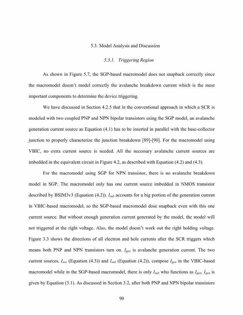
Figure 5.8 Simulated (a) base-emitter and collector-emitter voltages of the PNP and NPN transistors and (b) emitter, base and collector currents of the PNP and NPN transistors in the SGP-based macromodel.
93
Comparing with Figure 4.7, Figure 5.8(a) and (b) show the simulated voltages and
currents, respectively, versus the input voltage of the internal nodes of the PNP and NPN
transistors for the SGP-based macromodel. In Figure 5.8(a), the emitter-collector voltages of
both transistors also increase with increasing input voltage. The trigger voltage of the
macromodel by SGP model is higher than that of the one by VBIC model. After the SCR turns
on, the emitter-collector voltages reduce little bit and keep increasing afterwards while the base-
emitter voltages are in the range of 0.8-1.0 V. For the currents in Figure 5.8(b), very little current
goes through both transistors before triggering, while after triggering the current conduction
level of both transistors are low.
5.3.2. High Current Region
After the SCR device enters conduction mode, both PNP and NPN transistor turn on and
work in forward active mode. The simulated shape of I-V curve in conducting state depends on
the current level both PNP and NPN transistor models can work out. As shown in Figure 5.6,
Figure 4.7 and Figure 5.8, the conduction current level of SGP-based macromodel is low after
the model turns on while the VBIC-based macromodel can give the accurate conduction current.
After the device is triggered, considerable electrons and holes are injected from the
emitters of NPN and PNP transistor, and the SCR resistance is reduced significantly. As shown
in Figure 4.7 and Figure 5.8, the base-emitter biases of PNP and NPN transistors in both
macromodels are higher than those of the BJT transistors under normal analog applications,
especially the biases in the VBIC-based macromodel. This means the free-carrier injection level
in the SCR is extremely high. The high-level injection can also give rise to base pushout and
94
conductivity modulation in the collector. This effect is accounted for in the VBIC model with the
quasi-saturation components described by Equation (4.5) to (4.9).
Additionally, the emitter-collector biases of PNP and NPN transistors in both
macromodels are also high, especially the biases in the SGP-based macromodel. This means the
reverse biases of base-collector junctions are high where effects of impact ionization become
significant. This effect has been taken care of by avalanche current model in VBIC as described
by Equation (4.3) to (4.4).
With aforesaid advanced features in VBIC model, the VBIC-based macromodel can
simulate the SCR characteristic in conduction region very well. Figure 5.9 shows the forward
Gummel-Poon plots (Figure 5.9(a)) and the output characteristics (Figure 5.9(b)) of VBIC and
SGP models for the NPN transistor in both macromodels under normal model extraction
conditions. Figure 5.9(a) is the forward Gummel-Poon plots when Vce = 2 V. Since the NPN
transistor is working under high Vbe bias for SCR modeling, so we focus on high Vbe region when
doing the model extraction of VBIC and SGP for NPN transistor. We tried to make the SGP
model can reach the same high current level as VBIC, sacrificing the low Vbe region. If we make
the Ib and Ic of SGP model match the ones of VBIC model in low Vbe region, the both currents
will drop much lower in the high Vbe region. In Figure 5.9(b), it can be seen that at different Vbe,
the Ic increases as Vce increasing in VBIC model while it keeps almost the same in SGP model,
which shows the capability of VBIC model to handle impact ionization.
Figure 5.9 The Gummel-Poon plots and output characteristics of VBIC and SGP model of NPN transistor under normal model extraction conditions.
96
When we applied the extracted VBIC and SGP models on NPN transistor for both
macromodels, the bias voltages of base-emitter and emitter-collector junctions of NPN transistor
in both macromodels are different after both macromodels enter conduction mode with the same
bias at Anode. The characteristics of NPN transistor in both macromodels are studied when the
voltage at Anode is 10.85 V, under which voltage both PNP and NPN transistors turn on,
working in forward active mode. When voltage at Anode is 10.85V, the total current dumped by
the VBIC-based macromodel is 288.8 mA while only 23.34 mA by SGP-based macromodel. In
VBIC-based macromodel, Vbe and Vce are 1.15 V and 3.65 V respectively, and IB-NPN and IC-NPN
are 75.7 mA and 213 mA respectively. In SGP-based macromodel, Vbe and Vce are 0.8 V and
9.47 V respectively, and IB-NPN and IC-NPN are 14.34 mA and 8.5 mA respectively. Figure 5.10 and
Figure 5.11 show the comparison of forward Gummel-Poon plots and output characteristics for
VBIC and SGP models under the above bias conditions. It can be seen there are about two orders
of magnitude difference between the collector currents as well as the injected emitter currents of
the NPN transistor in the VBIC-based macromodel and the SGP-based one when both
macromodels are conducting ESD current even though the VBIC model and SGP model have
been extracted in the way that they have almost the same current level under high Vbe region.
Being lacking of features to model high level injection and avalanche breakdown, the
macromodel using SGP for NPN transistor has not been able to model the current of the SCR
device in conduction mode.
97
0.0 0.5 1.0 1.510-14
10-13
10-12
10-1110-10
10-9
10-8
10-7
10-6
10-5
10-4
10-310-2
10-1
100
101
0.7 0.8 0.9 1.0 1.1 1.2 1.3 1.4 1.510-3
10-2
10-1
100
I b, Ic (A
)
Vbe
(V)
Ic=8.50e-3 A
Ib=1.43e-2 A
Ic=2.13e-1 A
Ib=7.57e-2 A
I B-N
PN, I
C-N
PN (A
)
Vbe (V)
VBIC-IB-NPN at Vce=3.65V VBIC-IC-NPN at Vce=3.65V SGP-IB-NPN at Vce=9.47V SGP-IC-NPN at Vce=9.47V
Figure 5.10 The Gummel-Poon plot of VBIC and SGP model of NPN transistor when the macromodels is in conduction mode with a voltage of 10.85 V at Anode.
VBIC-IC-NPN at Vbe= 1.15V SGP-IC-NPN at Vbe= 0.80V
Figure 5.11 The output characteristics of VBIC and SGP model of NPN transistor when the macromodels is in conduction mode with a voltage of 10.85 V at Anode.
5.3.3. Negative Operation Region
The negative characteristic of the HH-LVTSCR is like a forward-biased diode, as the
TLP measurements in Figure 5.6. With the terminal connection as in Figure 5.3 and Figure 5.4,
when under the reverse bias, the P-Well/N-Well and P-Substrate/N-Well junction diodes are
forward biased and diode-mode conduction results. The P-Substrate/N-Well junction has been
modeled by Dsub. The current path going through Dsub under reverse bias is denoted as P1 in
99
Figure 5.3(a) and Figure 5.4(a). The P-Well/N-Well junction is the base-collector junction of the
PNP transistor as well as the NPN transistor. It has been modeled within the respective SGP-PNP
model and VBIC-NPN model in the VBIC-based macromodel, and SGP-PNP model and SGP-
NPN model in the SGP-based macromodel. The current path going through P-Well/N-Well
junction diode under reverse bias is denoted as P2 in Figure 5.3(a) and Figure 5.4(a). There is
one more current path going through the base-collector junction of the Parasitic-PNP transistor
built in VBIC, denoted as P3 (see Figure 5.3(a)).
For the SGP-based macromodel, there are only current path P1 and P2, the simulation
results can not fit the TLP measurement results since the coupled PNP and NPN transistor
models can not function correctly as a forward biased diode under reverse bias. With the built-in
parasitic PNP transistor, we have additional current path, P3, parallel with P1 and P2 to conduct
more reverse current.
5.4. Chapter Summary
In this chapter, we presented two SCR macromodels by using VBIC model and SGP
model respectively to describe the NPN bipolar transistor in the macromodel. The simulation
results of the VBIC-based macromodel shows excellent match with measurements while those of
the SGP-based macromodel do not. Comparing with SGP-based macromodel, the VBIC-based
macromodel has one more current source, avalanche breakdown current, to contribute to the total
generation current, which makes the macromodel predict the trigger and holding voltages
correctly. In additional to the avalanche current model, the VBIC model models the quasi-
saturation behavior to describe high level injection, which makes the VBIC-based macromodel is
100
accurate in conduction mode. Moreover, the parasitic PNP built in VBIC model supplies
additional current path in negative operation, which make the simulation results of the VBIC-
based macromodel fit the TLP measurements well in reverse direction. Being lake of the above
advanced features, the SCR macromodel by using SGP for NPN transistor has not been a
successful model.
101
CHAPTER 6. CONCLUSIONS
ESD failure is a stringent reliability problem to semiconductor industry. Up to one third
of all ICs failure might be attributed to ESD. The dissertation firstly talks about how ESD events
happen and how they related to failures of integrated circuits, which is followed by models of
ESD events and characterization of ESD performance in ICs. Then the dissertation leads the
topic to how to reduce ICs failures due to ESD. One of the most important ways is to incorporate
on-chip ESD protection inside ICs. The main contributions of this dissertation are having
designed and integrated the novel ESD protection devices for low- and high-voltage applications
and having developed and implemented the accurate compact model of the ESD protection
device in SPICE-like circuit simulator to optimize ESD design and predict ESD performance at
pre-silicon stages.
A novel SCR device, called uSCR, has been presented in this dissertation for ESD
protection applications of low-voltage ICs. This is the first time an SCR can possess a trigger
voltage as low as 7 V without using any external triggering circuitry and a holding voltage as
high as 6 V without sacrificing the ESD robustness, while at the same time consuming an area of
only 2400 μm2. The ESD protection robustness of the uSCR in both positive and negative
operations exceeds 60 mA/μm, which enables ESD protection levels of +/- 8 kV HBM and +/- 2
kV CDM for a low voltage ICs.
For high voltage technologies, the first important issue the snapback-type ESD protection
device has to face is how to avoid latch-up. Increase the holding current is an efficient solution.
102
The holding current of SCR device is dependent on the avalanche multiplication factor, M, and
the current gains of the PNP and NPN transistors in SCR device. A novel high holding current
SCR (HHC-SCR) has been developed in this dissertation for high voltage applications and test
devices have been fabricated on the BiCMOS 0.6 μm process. The TLP measurement results
have shown that by reaching a maximal M(IC-PNP+IC-NPN), the HHC-SCR device has realized a
holding current as high as 24 mA/μm to effectively avoid latch-up and a high failure current (48
mA/μm) for ESD robustness. Additionally, without involving any external circuitry or extra
devices, the HHC-SCR device releases reliability weakness issues and accomplishes the
minimum area consumption.
In additional to the on-chip ESD protection design, this dissertation has presented a
comprehensive compact model of SCR for the simulation of integrated circuits subjected to a
pervasive CDM ESD event. The work illustrated the useful and effective macromodeling
approach of integrating the various industry standard models to describe the individual devices
imbedded in the SCR. In addition, the modeling of the avalanche current sources, substrate
parastics, and capacitances were discussed. The issue of parameter extraction was addressed as
well. This modeling approach offers simplicity, wide availability and compatibility with most
commercial simulators by taking advantage of using the advanced BJT model, VBIC. The
presented model is implemented into the industry standard Cadence SPICE to study the CMOS
circuit response to CDM stress. Application to 0.35-μm technology SPDT analog switch I/O
circuits demonstrates effectiveness in analyzing CDM response and quantitatively predicting
withstand levels.
103
In the end, this dissertation compared two SCR macromodels by using VBIC model and
SGP model respectively to describe the NPN bipolar transistor in the SCR macromodel. The
simulation results of the VBIC-based macromodel shows excellent match with measurements
while those of the SGP-based macromodel do not. The avalanche current model, the quasi-
saturation model and the parasitic substrate transistor model built in VBIC model give the VBIC-
based macromodel capability to predict the trigger and holding voltages correctly, to perform in
conduction model accurately and to the dump enough current in reverse operation region to fit
the TLP measurement results. Being lake of the above advanced features, the SCR macromodel
by using SGP for NPN transistor has not been able to be a successful model.
104
LIST OF REFERENCES
[1] A. Wang, On-Chip ESD Protection for Integrated Circuits, Boston: Kluwer Academic
Publishers, 2002.
[2] T. J. Green and W. K. Denson, “A review of EOS/ESD field failures in military
equipment,” in Proceedings of EOS/ESD Symposium, 1988, pp. 7-14.
[3] W. D. Greason, “Electrostatic discharge: A charge driven phenomenon,” in Proc.
EOS/ESD Symposium, vol. EOS-13, Sept. 1991, pp. 1-9.
[4] International Technology Roadmap for Semiconductors, http://www.itrs.net, 2007.
[5] SEMATECH International, “Critical reliability challenges for the international technology
roadmap for semiconductor (ITRS),” SEMATECH DOC ID # 03024377A-TR, 2003.
[6] A. Amerasekera and C. Duvvury, “The impact of technology scaling on ESD robustness
and protection circuit design,” IEEE Transaction Component, Packaging and
Manufacturing Technology, Part A, vol. 21, no. 4, pp. 314-320, June 1995.
[7] S. H. Voldman, L. Lanzerotti, W. Morris, and L. Rubin, “A review of electrostatic
discharge (ESD) in advanced semiconductor technology,” Journal of Microelectronics
Reliability, vol. 44, no. 1, pp. 33-46, Jan 2004.
[8] S. H. Voldman, “A review of latchup and electrostatic discharge (ESD) in BiCMOS RF
silicon germanium technologies: Part I-ESD”, Journal of Microelectronics Reliability, vol.
45, no. 2, pp. 323-340, Feb 2005.
105
[9] S. H. Voldman, “A review of CMOS latchup and electrostatic discharge (ESD) in bipolar
complimentary MOSFET (BiCMOS) Silicon Germanium technologies: Part II–Latchup,”
Journal of Microelectronics Reliability, vol. 45, no. 3-4, pp. 437-455, Apr 2005.
[10] R. Glenn Wagner, J. M. Soden, and C. F. Hawkins, “Extent and Cost of EOS/ESD Damage
in an IC Manufacturing Process,” in Proceedings of EOS/ESD Symposium, 1993, pp. 49-55.
[11] T. J. Green and W. K. Denson, “Review of EOS/ESD Field Failures in Military
Equipment,” in Proceedings of EOS/ESD Symposium, 1988, pp. 7-14.
[12] A. Amerasekera and C. Duvvury, ESD in Silicon Integrated Circuits, 2nd ed., England:
John Wiley, 2002.
[13] J. E. Vinson, J. C. Bernier, G. D. Croft and J. J. Liou, ESD Design and Analysis Handbook,
Boston: Kluwer Academic Publishers, 2003.
[14] S. H. Voldman, ESD Circuits and Devices. England: Wiley, 2006.
[15] D. G. Pierce and D. L. Durgin, “An overview of electrical overstress effects on
semiconductor devices,” in Proceedings of EOS/ESD Symposium, 1981, pp.120-131.
[16] D. G. Pierce, “Electrostatic Discharge (ESD) Failure Mechanisms”, EOS/ESD Tutorial
Notes, 1995, pp. C-1 to C-32.
[17] S. Dabral and T. J. Maloney, Basic ESD and I/O Design, John Wiley & Sons, Inc., 1998.
[18] T. S. Speakman, “A model for the failure of bipolar silicon integrated circuits subjected to
electrostatic discharge,” in Proceedings of International Reliability Physics Symposium,
1974, pp.60-67.
106
[19] M. J. Middendorf and T. Hausken, “Observed physical effects and failure analysis of
EOS/ESD in MOS devices,” in Proceedings of International Symposium for Testing and
Failure Analysis, 1984, pp. 205-213.
[20] JEDEC Solid State Technology Association, “Electrostatic Discharge (ESD) Sensitivity
Testing Human Body Model (HBM),” JESD22-A114E, Jan 2007, [Online] available:
http://www.jedec.org.
[21] Electrostatic Discharge Association, “Electrostatic Discharge Sensitivity Testing – Human
Body Model (HBM) Component Level,” ANSI/ESD STM5.1-2007, Nov 2007, [Online]