56
Design considerations for a Half Design considerations for a Half - - Bridge LLC resonant converter Bridge LLC resonant converter

Design considerations for a HalfDesign considerations for a Half--Bridge LLC resonant converterBridge LLC resonant converter

2
AgendaAgenda
• Why an HB LLC converter
• Configurations of the HB LLC converter and a resonant tank
• Operating states of the HB LLC
• HB LLC converter modeling and gain characteristics
• Primary currents and resonant cap dimensioning
• Secondary rectification design and output cap dimensioning
• Resonant inductance balance
• Transformer winding dimensioning and transformer construction

3
The LCD and PLASMA TV market is growing each year. These and also other markets call for an SMPS unit that can provide these features:
- Output power from 150 W up to 600 W- Universal mains- Active or passive PFC (given by needed power)- Limited width and space, no fan: limited air flow- Low standby power consumption- Consumer Electronics market: fierce competition
The above requirements can be fulfilled with an SMPS that provides:→ High power density→ Smooth EMI signature→ Cost effective solution with minimum component count
Why an LLC series resonant converter ?Why an LLC series resonant converter ?

4
Benefits of an LLC series resonant converterBenefits of an LLC series resonant converter• Type of serial resonant converter that allows operation in relatively
wide input voltage and output load range when compared to the other resonant topologies
• Limited number of components: resonant tank elements can be integrated to a single transformer – only one magnetic component needed
• Zero Voltage Switching (ZVS) condition for the primary switches under all normal load conditions
• Zero Current Switching (ZCS) for secondary diodes, no reverse recovery losses
Cost effective, highly efficient and EMI friendly solutionfor high and medium output voltage converters

5
AgendaAgenda
• Why an HB LLC converter
• Configurations of the HB LLC converter and a resonant tank
• Operating states of the HB LLC
• HB LLC converter modeling and gain characteristics
• Primary currents and resonant cap dimensioning
• Secondary rectification design and output cap dimensioning
• Resonant inductance balance
• Transformer winding dimensioning and transformer construction

6
Configurations of an HB LLC Configurations of an HB LLC –– single res. capsingle res. cap
- Higher input current ripple and RMS value- Higher RMS current through the resonant capacitor- High voltage (600 – 1500 V) resonant capacitor needed- Low cost- Small size / easy layout

7
Compared to the single capacitor solution this connection offers:- Lower input current ripple and RMS value (1/√2)- Resonant capacitors handle half RMS current- Capacitors with half capacitance are used- Low voltage ratings (450 V) for the resonant capacitors when clamping diodes D3, D4 perform an easy and cheap overload protection
Configurations of an HB LLC Configurations of an HB LLC –– split res. capsplit res. cap

8
Resonant tank configurations Resonant tank configurations –– discrete solutiondiscrete solutionResonant inductance is located outside of the transformerAdvantages:- Greater design flexibility (designer can setup any Ls and Lm value)- Lower radiated EMI emission
Disadvantages of this solution are:- Complicated insulation between primary and secondary windings- Worse cooling conditions for the windings - More components to be assembled

9
Leakage inductance of the transformer is used as a resonant inductance.Advantages:- Low cost, only one magnetic component is needed - Usually smaller size of the SMPS- Better cooling conditions for transformer windings- Insulation between primary and secondary side is easily achieved
Disadvantages:- Less flexibility (achievable Ls inductance range is limited)- Higher radiated EMI emission - LLC with integrated resonant tank operates in a slightly different way than the solution with discrete Ls- Strong proximity effect in the primary and secondary windings
Resonant tank configurations Resonant tank configurations –– integrated solutionintegrated solution

10
AgendaAgenda
• Why an HB LLC converter
• Configurations of the HB LLC converter and a resonant tank
• Operating states of the HB LLC
• HB LLC converter modeling and gain characteristics
• Primary currents and resonant cap dimensioning
• Secondary rectification design and output cap dimensioning
• Resonant inductance balance
• Transformer winding dimensioning and transformer construction

11
sss LC
F⋅⋅⋅
=π2
1
)(21
minmss LLC
F+⋅⋅⋅
=π
LLC converter can operate:a) between Fmin and Fs c) above Fsb) direct in Fs d) between Fmin and Fs - overload
e) below Fmin
Operating states of the LLC converter Operating states of the LLC converter
Two resonant frequencies can be defined:
Discrete resonant tank solution

12
c) Operating waveforms for Fop > Fs Discrete resonant tank solution
CBA D E F
Operating states of the LLC converter Operating states of the LLC converter

13
- Integrated resonant tank behaves differently than the discrete resonant tank - leakage inductance is given by the transformer coupling - Llk participates only if there is a energy transfer between primary and secondary- Once the secondary diodes are closed under ZCS, Llk has no energy
Secondary diodes are always turned OFF under ZCS condition in HB LLC. The resonant inductance Ls and magnetizing inductance Lm never participate inthe resonance together as with discrete resonant tank solution!
m
lk
LLM −= 1
Operating states of the LLC converter Operating states of the LLC converter Integrated resonant tank solution

14
sss LC
F⋅⋅⋅
=π2
1
ms LCF
⋅⋅⋅=
π21
min
LLC converter can again operate:a) between Fmin and Fs c) above Fsb) direct in Fs d) between Fmin and Fs – overload
e) below Fmin
Two resonant frequencies can be defined:
Integrated resonant tank solutionOperating states of the LLC converter Operating states of the LLC converter

15
AgendaAgenda
• Why an HB LLC converter
• Configurations of the HB LLC converter and a resonant tank
• Operating states of the HB LLC
• HB LLC converter modeling and gain characteristics
• Primary currents and resonant cap dimensioning
• Secondary rectification design and output cap dimensioning
• Resonant inductance balance
• Transformer winding dimensioning and transformer construction

16
LLC converter modeling LLC converter modeling –– equivalent circuitequivalent circuitLLC converter can be described using firs fundamental approximation. Only approximation – accuracy is limited!! Best accuracy is reached around Fs.
Transfer function of equivalent circuit:21
2
ZZZ
VVnGin
outac +
=⋅
=
Z1, Z2 are frequency dependent => LLC converter behaves like frequencydependent divider. The higher load, the Lm gets to be more clamped by Rac. Resonant frequency of LLC resonant tank thus changes between Fs and Fmin.

17
Real load resistance has to be modified when using fundamental approximation because the real resonant tank is driven by square wave voltage.
ORMSac II22_
π=
ORMSac VVπ
22_ =
Considering the fundamental component of the square wave, the RMS voltage is:
In a full-wave bridge circuit the RMS current is:
LO
O
RMSac
RMSacac R
IE
IV
R 22_
_ 88ππ
===
The AC resistance Rac ca be expressed as:
LLC converter modeling LLC converter modeling –– equivalent circuitequivalent circuit

18
0
2
ZRnQ L⋅
=s
s
CLZ =0
s
m
LLk =
Resonant tank equationsResonant tank equations
sss LC
F⋅⋅⋅
=π2
1)(2
1min
mss LLCF
+⋅⋅⋅=
π
Quality factor: Characteristic impedance:
Lm/Ls ratio:
Minimum resonant frequency:Series resonant frequency:
Load dependent !
in
fout
VVV
G)(2 +⋅
=
Gain of the converter:

19
0.0
0.2
0.4
0.6
0.8
1.0
1.2
1.4
1.6
1.8
2.0
0.0 0.2 0.4 0.6 0.8 1.0 1.2 1.4 1.6 1.8 2.0
f / fs
volta
ge g
ain
Q=0.05Q=0.5Q=1Q=2Q=3Q=4Q=5Q=10Q=20Q=50Q=100Q=200
Lm/Ls=6Region 2
Region 1
Region 3
Normalized gain characteristicNormalized gain characteristic
Region 3: ZCS region Region 1 and 2: ZVS operating regions
Q=0.05 – Heavy load
ZCS
ZVS
Q=200 – Light load

20
Gain characteristic discussionGain characteristic discussion- The desired operating region is on the right side of the gain characteristic (negative slope means – ZVS mode for primary MOSFETs).
-Gain of the LLC converter, which operates in the fs is 1 (for discrete resonant tank solution) - i.e. is given by the transformer turns ratio. This operating point isthe most attractive from the efficiency and EMI point of view – sinusoidal primarycurrent, MOSFETs and secondary diodes optimally used. This operating point can be reached only for specific input voltage and load (usually full load andnominal Vbulk).
Gain characteristics shape and also needed operating frequency range is givenby these parameters:- Lm/Ls ratio- Characteristic impedance of the resonant tank- Load value- Transformer turns ratio

21
How to obtain gain characteristics?How to obtain gain characteristics?Use fundamental approximation and AC simulation in any simulation softwarelike PSpice, Icap4 etc..
Rac is the parameter !1 V amplitude AC supply
Direct gain plot for given Rac

22
Simulation schematic for discrete solution
Simulation schematic for integrated solution
Discrete and integrated tank gain differencesDiscrete and integrated tank gain differences

23
Full load Q and k factors optimization Full load Q and k factors optimization Proper selection of these two factors is the key point for the LLC resonantconverter design! Their selection will impact these converter characteristics:
- Needed operating frequency range for output voltage regulation- Line and load regulation ranges- Value of circulating energy in the resonant tank- Efficiency of the converter
The efficiency, line and load regulation ranges are usually the most importantcriteria for optimization.
Quality factor Q directly depends on the load. It is given by the Ls and Cscomponents values for full load conditions:
s
s
L
CLRnQ ⋅
=2

24
0.000
0.050
0.100
0.150
0.200
0.250
1.00E+04 1.00E+05 1.00E+06
Frequency [Hz]
Gai
n [-
]
Q=2 Q=3 Q=4
n=8, Ls/Lm=6, Q=parameter, Rload=2.4Ω
Gmin
Gmax
Δ f@Q=4
Δ f@Q=3
Needed gains band for full load regulation
- Higher Q factor results in larger Fop range - Characteristic impedance has to be lower for higher Q and given load => higher Cs- Low Q factor can cause the loss of regulation capability!- LLC gain characteristics are degraded to the SRC for very low Q values.
Full load Q and k factors optimization Full load Q and k factors optimization

25
- The k=Lm/Ls ratio dictates how much energy is stored in the Lm. - Higher k will result in the lover magnetizing current and gain of the converter. - Needed regulation frequency range is higher for larger k factor.
0.000
0.050
0.100
0.150
0.200
0.250
1.00E+04 1.00E+05 1.00E+06
Frequency [Hz]
Gai
n [-
]
k=2 k=4 k=6 k=8 k=10
Gmax
Gmin
Needed gains band for full load regulation
Δ f@k=6
Δ f@k=2
n=8, Cs=33nF, Ls=100uH, Lm=parameter, Rload=2.4Ω
Full load Q and k factors optimization Full load Q and k factors optimization

26
Practically, the Ls (i.e. leakage inductance of the integrated transformer version)has only limited range of values and is given by the transformer construction (forneeded power level) and turns ratio.
The Q factor calculation is then given by the wanted nominal operating frequency fs.
The k factor has to be then calculated to assure gains needed for the outputvoltage regulation (with line and load changes).
The k factor can be set in such a way that converter wont be able to maintainregulation at light loads – skip mode can be easily implemented to lover no loadconsumption.
Full load Q and k factors optimization Full load Q and k factors optimization

27
AgendaAgenda
• Why an HB LLC converter
• Configurations of the HB LLC converter and a resonant tank
• Operating states of the HB LLC
• HB LLC converter modeling and gain characteristics
• Primary currents and resonant cap dimensioning
• Secondary rectification design and output cap dimensioning
• Resonant inductance balance
• Transformer winding dimensioning and transformer construction

28
Fsw = Fs
Primary currents Primary currents –– single resonant capsingle resonant capIIN, IDM1
ICs
Time
2.780ms 2.782ms 2.784ms 2.786ms 2.788ms 2.790ms 2.792ms 2.794ms 2.796ms 2.798msV(Cs2:2)
0V
100V
200V
300V
400V
VCs
Time
3.26000ms 3.26400ms 3.26800ms 3.27200ms 3.27600ms 3.28000ms 3.28400ms3.25665ms 3.28740ms-I(IDM1)
-2.0A
-1.0A
-0.0A
1.0A
2.0A
IDM2
Time
3.26000ms 3.26400ms 3.26800ms 3.27200ms 3.27600ms 3.28000ms 3.28400ms3.25665ms 3.28740ms-I(IDM2)
-2.0A
-1.0A
-0.0A
1.0A
2.0A
⎟⎟⎠
⎞⎜⎜⎝
⎛
⋅⋅+
⋅⋅≈ 22
2
2
22
_ 1681
swm
bulkoutRMSC fL
Vn
IIs
πms LprimaryC I
nIII +== sec
Time
2.8160ms 2.8200ms 2.8240ms 2.8280ms 2.8320ms 2.8360ms 2.8400msI(Cs2) I(L5) -I(TX1)
-2.0A
-1.0A
-0.0A
1.0A
2.0A

29
Time
1.3200ms 1.3240ms 1.3280ms 1.3320ms 1.3360ms 1.3400ms 1.3440ms 1.3479msI(Cs)
-2.0A
-1.0A
-0.0A
1.0A
2.0A
Time
1.3200ms 1.3240ms 1.3280ms 1.3320ms 1.3360ms 1.3400ms 1.3440ms 1.3479msI(Cs2)
-2.0A
-1.0A
-0.0A
1.0A
2.0A
Time
1.9680ms 1.9720ms 1.9760ms 1.9800ms 1.9840ms 1.9880ms1.9648ms-I(V1)
-1.00A
0A
1.00A
2.00A
-1.49A
2.54A
Time
1.320ms 1.325ms 1.330ms 1.335ms 1.340ms 1.345ms 1.350msV(Cs2:2)
0V
100V
200V
300V
400V
IINICs2VCs2
ICs1
Time
3.26000ms 3.26400ms 3.26800ms 3.27200ms 3.27600ms 3.28000ms 3.28400ms3.25665ms 3.28740ms-I(IDM1)
-2.0A
-1.0A
-0.0A
1.0A
2.0A
IDM1
IDM2
Time
3.26000ms 3.26400ms 3.26800ms 3.27200ms 3.27600ms 3.28000ms 3.28400ms3.25665ms 3.28740ms-I(IDM2)
-2.0A
-1.0A
-0.0A
1.0A
2.0A
Primary currents Primary currents –– split resonant cap split resonant cap
Fsw=Fs

30
Single and split resonant capacitor solutions - 24 V / 10 A applicationComparison of Primary CurrentsComparison of Primary Currents
1.08 A2.16 AIIN_Pk
0.76 A1.07 AIIN_RMS
0.76 A1.52 AICs_RMS
1.08 A2.16 AICs_Pk
Split CapsSingle CapParameter
• Split solution offers 50% reduction in resonant capacitor current and 30% reduction in input rms current
• Select resonant capacitor(s) for current and voltage ratings

31
- Body diode is conducting during the dead time only (A)- MOSFET is conducting for the rest of the period (B) - Turn ON losses are given by Qg (burned in the driver not in MOSFET)- MOSFET turns OFF under non-zero current => turn OFF losses
Primary switches dimensioning Primary switches dimensioning
Time
3.26800ms 3.27200ms 3.27600ms 3.28000ms 3.28400ms3.26620ms 3.28707ms-I(IDM1) (V(M1:g)- V(bridge))/10 V(M2:g)/10
-1.0A
0A
1.0A
2.0A
A B

32
MOSFET RMS current calculation- The body diode conduction time is negligible- Assume that the MOSFET current has half sinusoid waveform
⎟⎟⎠
⎞⎜⎜⎝
⎛
⋅⋅+
⋅⋅≈ 22
2
2
22
_ 16161
swm
bulkoutRMSswitch fL
Vn
II π
swm
bulkOFF fL
VI⋅⋅
≈8
Turn OFF current calculation- Assume that the magnetizing current increases linearly
- Turn OFF losses (EOFF @ IOFF) can be find in the MOSFET datasheet
Primary switches dimensioningPrimary switches dimensioning
OFFdsONRMSswitchtotalswitch PRIP +⋅≈ 2__

33
AgendaAgenda
• Why an HB LLC converter
• Configurations of the HB LLC converter and a resonant tank
• Operating states of the HB LLC
• HB LLC converter modeling and gain characteristics
• Primary currents and resonant cap dimensioning
• Secondary rectification design and output cap dimensioning
• Resonant inductance balance
• Transformer winding dimensioning and transformer construction

34
Secondary Rectifier DesignSecondary Rectifier Design• Secondary rectifiers work in ZCS• Possible configurations:
a) Push-Pull configuration – for low voltage / high current output
b) Bridge configuration – for high voltage / low current output
c) Bridge configuration with two secondary windings – for complementary output voltages
Advantages:- Half the diode drops compared to bridge- Single package, dual diode can be used - Space efficient
Disadvantages:- Need additional winding- Higher rectifier breakdown voltage- Need good matching between windings
Push-Pull Configuration

35
Equations 24 V/10 A output
RMS diode current
4_π
⋅= outRMSD II
2_out
AVGDII =
2_π
⋅= outPKD II
AVG diode current
Peak diode current
AI RMSD 85.7_ =
AI AVGD 5_ =
AI PKD 7.15_ =
12 V/20 A output
AI PKD 4.31_ =
AI AVGD 10_ =
AI RMSD 7.15_ =
Secondary Current Calculations Secondary Current Calculations –– PushPush--PullPull
• To simplify calculations, assume sinusoidal current and Fop=Fs

36
Equations 24 V/ 10 AVf=0.8 V, Rd=0.01 Ohm
Losses due to forward drop:
2OUTF
DFWIVP ⋅
=
16
22 π⋅⋅= OUTd
DRdIRP
Losses due to dynamic resistance:
rectDRdDFWtotalct nPPP ⋅+= )(_Re
W0.4=DFWP
W62.0=DRdP
W24.9_Re =totalctP
12 V/ 20 AVf=0.5 V, Rd=0.01 Ohm
W48.2=DRdP
W0.5=DFWP
Equation 24 V/ 10 A 12 V/ 20 A
W15_Re =totalctP
Rectifier Losses Rectifier Losses –– PushPush--PullPull

37
Advantages:- Lower voltage rating - Needs only one winding- No matching needed for windings
Disadvantages:- Higher diode drops- Need four rectifiers
Secondary Rectifiers Secondary Rectifiers -- Bridge ConfigurationBridge Configuration

38
1. Select appropriate topology (push-pull or bridge) 2. Calculate rectifier peak, AVG and RMS current3. Select rectifier based on the needed current and voltage ratings4. Measure the diode voltage waveform in the application and design
snubber to limit diode voltage overshoot and improve EMI signature (forLLC “weak” snubber is needed since diodes operate in ZCS mode)
Notes:
- The current ripple increases for fop<fs, the current waveform is still half “sinusoidal” but with dead times between each half period
- The peak current is very high for low voltage and high current LLC applications – example 12 V/ 20 A output: Ipeak= 31.4 A and IRMS= 9.7 A!! Each “mΩ” becomes critical - PCB layout. The secondary rectification paths should be as symmetrical as possible to assure same parameters for each switching cycle.
Secondary Rectifier Design ProcedureSecondary Rectifier Design Procedure

39
• Output capacitor is the only energy storage device – Higher peak/rms ripple current and energy
• Ripple current leads to:– Voltage ripple created by the ESR of output capacitor (dominant)– Voltage ripple created by the capacitance (less critical)
Output Capacitor DimensioningOutput Capacitor Dimensioning

40
2_π
⋅= outpeakrect IIAI peakrect 7.15_ =
Equations: 24 V/ 10 A example:Cf=5000 uF, ESR=6 mΩ
peakrectpkpkrippleout IESRV ___ ⋅=−
mV 94__ =− pkpkrippleoutV
Peak rectifier current
Output voltage ripple peak to peak
ESR Component of Output RippleESR Component of Output Ripple• In phase with the current ripple and frequency independent• Low ESR capacitors needed to keep ripple acceptable
– Cost/performance trade-off (efficiency impact)
18
2
_ −⋅=π
outRMSCf II A83.4_ =RMSCfICapacitor RMS current:
ESRIP RMSCfESR ⋅= 2_
mW 140=ESRPESR power losses

41
Capacitive Component of Output RippleCapacitive Component of Output Ripple
• Out of phase with current and frequency dependent• Actual ripple negligible due to high value of
capacitance chosen
Equation: 24 V/ 10 A output example:Cf=5000 uF, Fop=100 kHz
)2(32___ −⋅
⋅⋅⋅⋅=− π
π fop
outpkpkcaprippleout Cf
IV
mV 1.2__ =caprippleoutV
24 V/ 10 A output example:Cf=100 uF, Fop=100 kHz
mV 104__ =caprippleoutV
42
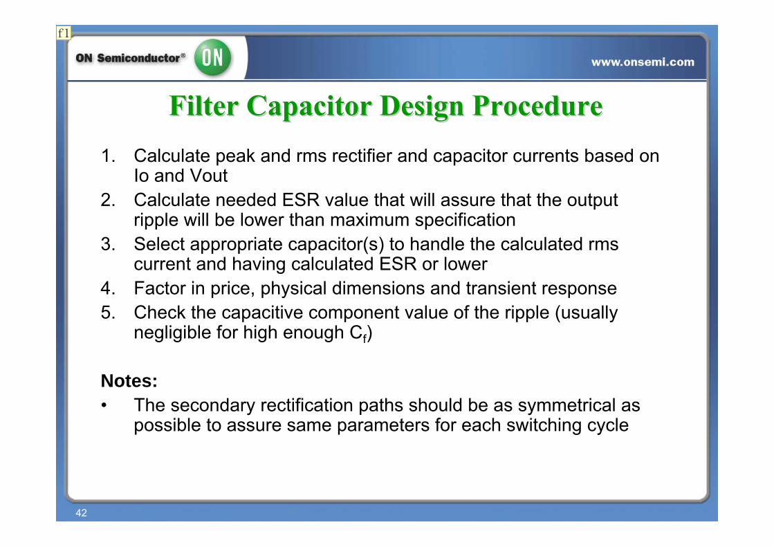
Filter Capacitor Design ProcedureFilter Capacitor Design Procedure1. Calculate peak and rms rectifier and capacitor currents based on
Io and Vout2. Calculate needed ESR value that will assure that the output
ripple will be lower than maximum specification3. Select appropriate capacitor(s) to handle the calculated rms
current and having calculated ESR or lower4. Factor in price, physical dimensions and transient response5. Check the capacitive component value of the ripple (usually
negligible for high enough Cf)
Notes:• The secondary rectification paths should be as symmetrical as
possible to assure same parameters for each switching cycle
f1

幻灯片 42
f1 This slide may be better off getting split into two slides and add some more notes. Let's discuss. ffmrmw, 2007-9-3

43
AgendaAgenda
• Why an HB LLC converter
• Configurations of the HB LLC converter and a resonant tank
• Operating states of the HB LLC
• HB LLC converter modeling and gain characteristics
• Primary currents and resonant cap dimensioning
• Secondary rectification design and output cap dimensioning
• Resonant inductance balance
• Transformer winding dimensioning and transformer construction

44
Resonant inductance balanceResonant inductance balance
Example:Llk(p-s1) = 105 uHLlk(p-s2) = 115 uH∆Llk = 10 uHLlk(total) = 100 uHLm = 600 uHCs = 33 nF
- Total Ls is always affected by the transformer leakage inductance - Special case for transformer with integrated leakage inductance - Ls=Llk- Push pull and mult. output app. are sensitive to the leakage inductance balance
C-D openD-E open
A-BLm
C-D shortD-E short
A-BLlk(total)
C-D openD-E short
A-BLlk(p-s2)
C-D shortD-E open
A-BLlk(p-s1)
Secondary pins configuration
Measuredbetween
pins
Parameter
fs1 = 85.5 kHz
fs2 = 81.7 kHz5 % difference
Transformer leakage inductance

45
Resonant inductance balanceResonant inductance balanceSeries resonant frequency differs for each switching half-cycle that resultsin primary and mainly secondary current imbalance.
Time
608.00us 612.00us 616.00us 620.00us 624.00us 628.00us 632.00us 635.45usI(D6) I(D3)
0A
4A
8A
12A
16A
3 A difference in the peak secondary current – the power dissipation is differentfor each rectifier from pair as well as for the secondary windings.

46
Resonant inductance balanceResonant inductance balance
Converter works below series resonant frequency Fs for the one half of theswitching cycle and in the Fs for the second half of the switching cycle.
Iprimary

47
Resonant inductance balanceResonant inductance balanceFor high power app. it is attractive to connect primary windings in series andsecondary windings in parallel. There is possibility to compensate transformerleakage imbalance by appropriate connection of the secondary windings:
∆Llk_total = 2* ∆Llk ∆Llk_total = 0

48
Resonant inductance balanceResonant inductance balanceThe secondary leakage inductance is transformed to the primary and increasesthe total resonant inductance value. Situation becomes critical for the LLC applications with high turns ratios.
12 V / 20 A application example:Np = 35 turns Llk_s1 = 100 nHNs = 2 x 2 turns Llk_s2 = 150 nHn = Np/Ns = 17.5Ls = 110 uHLm = 630 uH
∆Llk_s = 50 nH HnLL slks μ3.152_ =⋅Δ=Δ
50 nH difference on the secondary causes 14 % difference of Ls !!!

49
Transformer construction and secondary layout considerations:
- Resonant tank parameters can change each switching half cycle when push pull configuration is used. This can cause the primary and secondary currents imbalance.
- For the transformer with integrated resonant inductance, it has to be checked how the transformer manufacturer specifies the leakage inductance. Specification for all secondary windings shorted is irrelevant. The particular leakage inductance values can differ.
- When using more transformers with primary windings in series andsecondary windings in parallel the leakage inductance asymmetry can be compensated by appropriate secondary windings connection.
- Secondary leakage inductance can cause significant resonant inductance imbalance in applications with high transformer turns ratio. Layout on the secondary side of the LLC resonant converter is critical in that case.
Resonant inductance balanceResonant inductance balance

50
AgendaAgenda
• Why an HB LLC converter
• Configurations of the HB LLC converter and a resonant tank
• Operating states of the HB LLC
• HB LLC converter modeling and gain characteristics
• Primary currents and resonant cap dimensioning
• Secondary rectification design and output cap dimensioning
• Resonant inductance balance
• Transformer winding dimensioning and transformer construction

51
The primary current is sinusoidal for Fop=Fs. The secondary current is almostsinusoidal too – there is slight distortion that is given by the magnetizing current.
Transformer winding dimensioningTransformer winding dimensioning
⎟⎟⎠
⎞⎜⎜⎝
⎛
⋅⋅+
⋅⋅≈ 22
2
2
22
_ 1681
swm
bulkoutRMSprimary fL
Vn
II π
22_sec ⋅⋅≈
πoutRMSondary II
- The skin effect and mainly proximity effect decreases effective cooper area. - Proximity effect can be overcome by the interleaved winding construction (for
discrete resonant tank solution)
- The proximity effect becomes critical for the transformer with integrated leakage- Wires that are located to the center of the bobbin “feels” much higher current density than the rest of the windings even when litz wire used!
(single winding solution)

52
Transformer with integrated leakageTransformer with integrated leakage- For the standard transformer with good coupling (Llk<0.1*Lm) is the leakageinductance independent on the air gap thickness and position
m
lk
LLM −= 1
- Transformer with divided bobbin exhibits high leakage inductance- Significant energy is related to the stray flux - The Llk is dependent on air gap thickness and position

53
- Small energy is stored in the Lm each switching cycle to prepare ZVS - Lm is given by the magnetic conductivity of the magnetic circuit i.e.: Lm=n2*Al- Gap is used to absorb most of the magnetizing energy and to adjust Lm value- Magnetizing energy is taken from the primary winding - it is advantageous tolocate the air gap in the centre of the primary winding
Transformer with integrated leakageTransformer with integrated leakage

54
ConclusionsConclusions• HB LLC Converter provides a very good solution for high efficiency,
low EMI power conversion requirements• Design considerations for HB LLC converter are more complex than
traditional topologies– Transformer design choice is critical for converter operation– Other passive components also exhibit high stresses– Frequency variation is used to maintain output regulation
• This presentation covered all power stage design considerations– More details available in future app. note
• ON Semiconductor offers full support for your designs using NCP1395/1396

55
Thank you for your attention!


