1560 IEEE JOURNAL OF PHOTOVOLTAICS, VOL. 8, NO. 6, NOVEMBER 2018
Design Criteria for Micro-Optical TandemLuminescent Solar Concentrators
David R. Needell , Ognjen Ilic, Colton R. Bukowsky , Zach Nett, Lu Xu, Junwen He, Haley Bauser ,Benjamin G. Lee , John F. Geisz , Ralph G. Nuzzo, A. Paul Alivisatos, and Harry A. Atwater
Abstract—Luminescent solar concentrators (LSCs) harnesslight generated by luminophores embedded in a light-trappingwaveguide to concentrate onto smaller cells. LSCs can absorb bothdirect and diffuse sunlight, and thus can operate as flat plate re-ceivers at a fixed tilt and with a conventional module form factor.However, current LSCs experience significant power loss throughparasitic luminophore absorption and incomplete light trapping bythe optical waveguide. Here, we introduce a tandem LSC device ar-chitecture that overcomes both of these limitations, consisting of apoly(lauryl methacrylate) polymer layer with embedded cadmiumselenide core, cadmium sulfide shell (CdSe/CdS) quantum dot (QD)luminophores and an InGaP microcell array, which serves as highbandgap absorbers on the top of a conventional Si photovoltaic.We investigate the design space for a tandem LSC, using experi-mentally measured performance parameters for key components,including the InGaP microcell array, CdSe/CdS QDs, and spec-trally selective waveguide filters. Using a Monte Carlo ray-tracingmodel, we compute the power conversion efficiency for a tandemLSC module with these components to be 29.4% under partiallydiffuse illumination conditions. These results indicate that a tan-dem LSC-on-Si architecture could significantly improve upon theefficiency of a conventional Si photovoltaic cell.
Index Terms—III–V concentrator photovoltaics (PV), lumines-cent devices, Monte Carlo methods, quantum dots (QDs), tandemPV.
I. INTRODUCTION
LUMINESCENT solar concentrators (LSCs) offer a methodto capture diffuse sunlight and maintain a relatively low
manufacturing cost [1]. A traditional LSC consists of an optical
Manuscript received March 9, 2018; revised May 19, 2018; accepted July22, 2018. Date of publication August 10, 2018; date of current version Oc-tober 26, 2018. This work was supported by the U.S. Department of Energy,Advanced Research Projects Agency for Energy under Grant DE-AR0000627.(Corresponding author: Harry A. Atwater.)
B. G. Lee and J. F. Geisz are with the National Renewable Energy Laboratory,Golden, CO 80401 USA (e-mail:,[email protected]; [email protected]).
A. P. Alivisatos is with the Lawrence Berkeley National Laboratory,Department of Materials Science and Engineering, and Kavli EnergyNanoScience Institute, University of California Berkeley, Berkeley, CA 94720USA (e-mail:,[email protected]).
Color versions of one or more of the figures in this paper are available onlineat http://ieeexplore.ieee.org.
Digital Object Identifier 10.1109/JPHOTOV.2018.2861751
waveguide with luminophores suspended in a polymer matrixand photovoltaics (PV) material lining the waveguide’s edges[2]–[4]. Both diffuse and direct sunlight incident upon this wave-guide become absorbed by the embedded luminophores.
Such absorbed photons can undergo radiative recombination,which gives rise to a sharply peaked and energy downshiftedphotoluminescence (PL) emission spectrum. As dictated by thephotoluminescence quantum yield (PLQY) of the luminophoreabsorbers, photons can also undergo nonradiative recombina-tion, becoming parasitically lost as heat. Total internal reflectiontypically guides the PL radiation to the waveguide’s edge, whereit impinges upon the PV cells [5]–[7]. The light concentrationfactor is, therefore, proportional to the geometric gain (GG) ofthe LSC, defined as the ratio of illuminated waveguide area tototal PV cell area.
Despite extensive research and development, LSC moduleconcentration factors and power conversion efficiencies (PCEs)suffer from two key loss mechanisms [8]–[10]. First, embed-ded luminophores require near-unity PLQY in order to achievedesired optical efficiencies [11]. To prevent excess nonradia-tive recombination, overlap between luminophore absorbed andemitted photon energies needs to be minimized by employing lu-minophore species that exhibit a Stokes shift [12]–[14]. Despiteadvances in PLQY of various organic dyes and fluorophores,luminophores have not been traditionally able to exhibit botha sufficiently high PLQY and large Stokes shifts, leading to asignificant fraction of luminesced photons to be re-absorbed bythe luminophores [10], [15]–[19]. Second, the index of refrac-tion contrast between the optical waveguide and the surround-ing medium defines a photon escape cone and the limits forwaveguide light trapping [13]. The LSC, therefore, experiencessignificant escape cone losses for light photoluminescence atangles that lie between normal incidence and the critical angleof the waveguide.
Recent advances in cadmium selenide core, cadmium sul-fide shell (CdSe/CdS) quantum dots (QDs) allow for near-unityPLQY at sufficiently large Stokes shifts and ratios—where wedefine the Stokes shift and ratio as the separation of absorp-tion and PL bands and the ratio of the absorption at the CdSto CdSe band edges, respectively [14], [20]. Furthermore, asshown by previous studies, the incorporation of top and bottomspectrally selective filters presents a possible approach to en-hancing the waveguide light trapping efficiency [10], [12], [15],[21]–[23]. Despite these solutions targeted to maximize the op-tical efficiency of an LSC, only a small portion of incident light
NEEDELL et al.: DESIGN CRITERIA FOR MICRO-OPTICAL TANDEM LUMINESCENT SOLAR CONCENTRATORS 1561
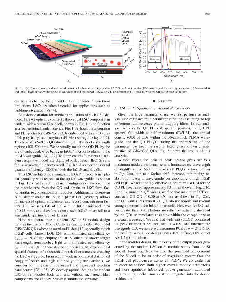
Fig. 1. (a) Three-dimensional and two-dimensional schematics of the tandem LSC–Si architecture, the QDs are enlarged for viewing purposes. (b) Measured Siand InGaP EQE curves with respect to wavelength and optimized CdSe/CdS QD absorption and PL spectra with reflectance regime definitions.
can be absorbed by the embedded luminophores. Given theselimitations, LSCs are often intended for applications such asbuilding-integrated PVs [4].
As a demonstration for another application of such LSC de-vices, here we optically connect a theoretical LSC component intandem with a planar Si subcell, shown in Fig. 1(a), to functionas a four-terminal tandem device. Fig. 1(b) shows the absorptionand PL spectra for CdSe/CdS QDs embedded within a 30-μm-thick poly(lauryl methacrylate) (PLMA) waveguide layer [12].This type of CdSe/CdS QD absorbs most in the short wavelengthregime (400–500 nm). We spectrally match the QD PL by theuse of embedded, wide bandgap InGaP microcells planar to thePLMA waveguide [24]–[27]. To complete this four-terminal tan-dem design, we model interdigitated back contact (IBC) Si cellsfor use as an example bottom cell. Fig. 1(b) displays the externalquantum efficiency (EQE) of both the InGaP and Si cells.
This LSC architecture arranges the InGaP microcells in a pla-nar geometry with respect to the optical waveguide, as shownin Fig. 1(a). With such a planar configuration, we decouplethe module area from the GG and obtain an LSC form fac-tor similar to conventional Si modules. Additionally, Bronsteinet al. demonstrated that such a planar LSC geometry allowsfor increased optical efficiencies and record concentration fac-tors [12]. We set a GG of 100 with an InGaP microcell areaof 0.15 mm2, and therefore expose each InGaP microcell to awaveguide aperture area of 15 mm2.
Here, we characterize a tandem LSC-on-Si module designthrough the use of a Monte Carlo ray-tracing model. We modelCdSe/CdS QDs whose absorption/PL data [12] spectrally matchInGaP cells’ known EQE [24] with simulated cell efficiencyηInGaP = 19.3% and employ an IBC Si subcell to absorb longerwavelength, nonabsorbed light with simulated cell efficiencyηSi = 18.2%. Using these device components, we explore idealspectral features of a theoretical notch-filter structure encasingthe LSC waveguide. From recent work in optimized distributedBragg reflectors and high contrast grating metasurfaces, weconsider both angularly independent and dependent rejectionband centers [28]–[35]. We develop optimal designs for tandemLSC-on-Si modules both with and without such notch-filtercomponents and analyze best-case simulation scenarios.
II. RESULTS
A. LSC-on-Si Optimization Without Notch Filters
Given the large parameter space, we first perform an anal-ysis with extensive multiparameter variations assuming no topor bottom luminescence photon-trapping filters. In our anal-ysis, we vary the QD PL peak spectral position, the QD PLspectral full width at half maximum (FWHM), the opticaldensity (OD) of QDs within the 30-μm-thick PLMA wave-guide, and the QD PLQY. During the optimization of oneparameter, we treat the rest as fixed given known charac-teristics of CdSe/CdS QDs. Fig. 2 shows the results of thisanalysis.
Without filters, the ideal PL peak location gives rise to amaximum module performance at a luminescence wavelengthof slightly above 650 nm across all PLQY values, shownin Fig. 2(a), due to a Stokes shift increase, minimizing re-absorption losses at wavelengths corresponding to high InGaPcell EQE. We additionally observe an optimum FWHM for theQD PL spectrum of approximately 80 nm, as shown in Fig. 2(b).For all assumed PLQY values, we find that maximum PCE oc-curs at a QD OD of 0.30 at 450 nm, as shown in Fig. 2(c).For OD values less than 0.30, QDs do not absorb and re-emitenough photons to the InGaP microcells. However, for OD val-ues greater than 0.30, photons are either parasitically absorbedby the QDs or reradiated at angles within the escape cone ata greater frequency. We find that with unity PLQY, optimizedPL peak location at 650 nm, ideal FWHM, and intermediatewaveguide OD, we achieve a maximum PCE of η = 24.5% forthe no-filter waveguide design under 40% diffuse, 60% directAM1.5 g simulations.
In the no-filter design, the majority of the output power gen-erated by the tandem LSC-on-Si module stems from the Sisubcell. From Fig. 2(d), we find the generated photocurrentof the Si cell to be an order of magnitude greater than theInGaP cell photocurrent across all PLQY. We conclude thatin order to achieve both higher overall module efficienciesand more significant InGaP cell power generation, additionallight-trapping mechanisms must be integrated into the devicearchitecture.
1562 IEEE JOURNAL OF PHOTOVOLTAICS, VOL. 8, NO. 6, NOVEMBER 2018
Fig. 2. Tandem LSC-on-Si module efficiency in the case without filters, with respect to varying. (a) PLQY and QD PL peak location assuming an OD of 0.30and FWHM of 30 nm. (b) PLQY and QD PL FWHM assuming an OD of 0.30 and PL peak location of 635 nm. (c) PLQY and OD of the embedded QDs at 450 nmassuming a PL peak location of 635 nm and FWHM of 30 nm. (d) Short-circuit current of the Si and InGaP cells, varying PLQY and OD of the embedded QDs at450 nm again assuming a PL peak location of 635 nm and FWHM of 30 nm.
B. Top and Bottom Notch-Filter Optimization
To determine optimal spectral and angular requirements forthe top and bottom luminescence photon trapping notch filters,we vary the reflection parameters, with a top hat-like profile, asshown in Fig. 1(c).
Given the PL spectrum of such CdSe/CdS QDs, Fig. 3(a)shows the module PCE for various rejection-band widths. Awidth of 68 nm yields maximum device performance, assum-ing no strong angular dependence of the rejection band of thenotch filter and a QD PL FWHM of 30 nm centered at 635 nm.Assuming ideal rejection-band top/bottom filter widths, we in-vestigate the effects of filter reflectance variation, specificallyRrejection against Rpass (in the short-pass and long-pass regimes).Fig. 3(c) details the overall module efficiency results, whilevarying the two reflection parameters Rrejection and Rpass. Wefind that, while optimal module efficiency results from an as-sumed unity Rrejection and zero Rpass, an increase in filter Rpass
is more detrimental to overall device performance than a re-duction in Rrejection. Assuming distinct top/bottom notch filters,we determine the overall impact on module efficiency of vary-ing Rshort-pass for the bottom notch filter only while assuming aunity Rrejection and zero Rpass for the top notch filter. Fig. 3(d)shows that the short-wavelength transmission requirements forthe bottom filter can be significantly relaxed while still enablinghigh performance. For the optimal top and bottom angularly in-
dependent notch-filter designs obtained from this analysis, weachieve a maximum module efficiency of η = 27.7%.
As is the case with common spectrally selective notch fil-ters (e.g., one-dimensional photonic crystals), a greater incidentphoton angle often blueshifts the rejection band while main-taining a relatively constant bandwidth [31], [30], [28]. We varythe rejection band left and right edges’ location for normallyincident photons, and, as an example, assume a rejection bandblue-shift of 1 nm per degree off-normal incidence. Fig. 3(b)shows the results of this simulation. For rejection band left andright edges located near 620 and 700 nm, respectively, we finda globally maximum module efficiency of η = 25.0%.
C. LSC-on-Si Optimization With Notch Filters
Analogous to the optimization of the tandem LSC withoutspectral filters, we determine the maximum module efficiencypossible with optimal top and bottom notch filters. Fig. 4(a)shows that ideal PL peak values depend strongly on the PLQY.For lower QD performance, 650 nm yields maximum moduleefficiency. As the limit of PLQY approaches unity, the PL peakoptimum shifts to 635 nm as a result of the lossless filters al-lowing for unlimited photon recycling and trapping.
Similarly, we see a strong dependence of module perfor-mance on PLQY by varying the FWHM, shown in Fig. 4(b). Wefind that, as expected, high PLQY values favor sharply peaked
NEEDELL et al.: DESIGN CRITERIA FOR MICRO-OPTICAL TANDEM LUMINESCENT SOLAR CONCENTRATORS 1563
Fig. 3. Tandem LSC-on-Si module efficiency with respect to varying. (a) Rejection-band filter width, centered at 635 nm, assuming unity rejection-band reflectionand unity out-band transmission. (b) Filter rejection-band left and right edges’ location at DNI photons, assuming unity Rrejection and zero Rpass. (c) Top andbottom filter Rrejection vs. Rpass across all angles at ideal rejection-band widths. (d) Bottom-only filter Rrejection vs. Rshort-pass, assuming ideal top filter performanceas shown in (c), and ideal rejection-band widths.
PL. Variation of OD of the QDs embedded within the polymerwaveguide shows a strong dependence on PLQY values as well,shown in Fig. 4(c). However, in all cases, a maximum modulePCE is obtained at OD of 0.30 at 450 nm. In contrast to theno-filter case, we find that the module efficiency decreases lessrapidly for increasing OD with nonunity PLQY. We, therefore,find that with unity PLQY, optimized QD PL peak location, idealFWHM, and an OD of 0.30 at 450 nm, we achieve a maximumPCE of η = 29.4% under 40% diffuse, 60% direct AM1.5 gsimulations.
D. Optimal Case Analysis
In the perfect-filter case, the output power generated by thistandem LSC-on-Si module is much more evenly split betweenthe Si subcell and the embedded InGaP microcells. The InGaPcontributes approximately 43% of the total output power forunity PLQY, as shown in Table I. Fig. 4(d) displays the short-circuit current contribution of the InGaP cell. In contrast toFig. 2(d), the InGaP photocurrent has increased by a factorof 4.5.
Fig. 5(b)–(d) compares the performance of the optimized no-filter and perfect-filter designs. For this, we choose a PLQY of0.98 to determine how parasitic QD absorption loss comparesto escape cone loss. We find that in the no-filter design, thelargest performance detriment comes from escape cone loss,shown in Fig. 5(c). For the perfect-filter case, short-wavelength
photons are more likely to be parasitically absorbed, as a re-sult of increased photon recycling, shown in Fig. 5(d). Wedemonstrate this fact by comparing the average number of PLevents for a given photon of a certain wavelength, shown inFig. 5(b). We note that even though CdSe/CdS exhibits largeStokes ratios [12], extended PL lifetimes result in more fre-quent re-absorption. The dominant loss mechanism for longwavelength photons in the perfect-filter design is primarily a re-sult of the imperfect absorption of the Si subcell, matching theno-filter case. This matches well to expected loss mechanismspreviously reported [36].
Table I shows the comparison between best-case scenarios ofthe no-filter and perfect-filter configurations, for unity and 0.98PLQY. Additionally, Table I compares the overall power outputwith the use of a 25.6% cell efficiency, silicon heterojunctionstructure with IBCs as the subcell [37]; we also demonstrate thepower output possible with this tandem LSC–Si architecture byreplacing the subcell with a passivated emitter with rear contact(PERC) Si cell [38].
Finally, we investigate how the fraction of DNI light affectsthe overall module PCE. Fig. 5(a) shows the results of this simu-lation for the perfect-filter case. As expected, the highest moduleefficiency results from 100% DNI; however, we also note thatthe absolute percent efficiency increase between the completelydiffuse case (i.e., 0% DNI) and the fully direct case is 0.389%absolute PCE for the LSC-on-Si module. This suggests that,while DNI light is ideal for maximum module efficiencies, this
1564 IEEE JOURNAL OF PHOTOVOLTAICS, VOL. 8, NO. 6, NOVEMBER 2018
Fig. 4. Tandem LSC–Si module efficiency in the perfect-filters case with respect to varying. (a) PLQY and QD PL peak location. (b) PLQY and QD PLFWHM. (c) PLQY and OD of the embedded QDs at 450 nm. (d) Short-circuit current of the Si and InGaP cells, varying PLQY and OD of the embedded QDsat 450 nm.
tandem LSC-on-Si architecture can perform close to 30% PCEeven in the completely diffuse limit. Debije et al. demonstratedanalogous results for an LSC’s performance under varyingdiffusivity conditions [1].
III. CONCLUSION
We have introduced a tandem-on-Si LSC design. We showsignificant PCE enhancements can be achieved in a tandemLSC, relative to both traditional single-layer LSC designs andflat-plate Si cells. A tandem LSC-on-Si module features anumber of components that influence its conversion effi-ciency, including spectrally selective top and bottom filtersand CdSe/CdS QD luminophores with optimally tuned ab-sorption and PL spectra. We apply a Monte Carlo ray-tracingmodel to IBC Si and InGaP cells with known EQEs, whichyield stand-alone, simulated cell efficiencies of ηSi = 18.2%and ηInGaP = 19.3% under direct AM1.5 conditions. We ulti-mately find, under 40% diffuse 60% direct AM1.5 g simulationconditions, maximum LSC-on-Si PCEs reach 24.5% and 29.4%for the no-filter and perfect-filter designs, respectively. Further-more, if we assume Si subcell EQEs consistent with reportedPERC [38] or heterojunction interdigitated back contact [37] Sicells and perfect notch filters, we find tandem LSC-on-Si PCEsof 31.2% and 32.0%, respectively.
Assuming a tandem structure without top and bottom filters,we find an ideal QD PL peak location of 650 nm given the InGaPand Si cell EQEs, optimized QD PL FWHM of 80 nm, and anOD of the embedded QDs within the PLMA waveguide of 0.30at 450 nm. For high QD PLQY under these conditions, we finda maximum PCE of 24.5%, where roughly 10% of this poweris generated by the LSC and 90% by the Si subcell.
Optimizing the top and bottom notch filters’ spectral reflec-tion and angular dependence for maximum PCE, we find fornear-unity PLQY an ideal QD PL peak location of 635 nm, op-timized QD PL FWHM of 10 nm, and an OD of the embeddedQDs within the PLMA waveguide of 0.30 at 450 nm. Underthese conditions and optimized filter design, we find a maxi-mum PCE of 29.4%, where roughly 45% of the output power isgenerated by the LSC and 55% by the Si subcell.
IV. METHODS
The tandem LSC-on-Si module performance is simulatedvia a Monte Carlo ray-tracing model [39]–[41]. The algorithmtraces photons throughout the module architecture, assumingperiodic boundary conditions at the waveguide edges. We deter-mine photon trajectories via scattering, reflection, transmission,and absorption probabilities for each component in the device.We calculate photon reflection probabilities by Fresnel laws for
NEEDELL et al.: DESIGN CRITERIA FOR MICRO-OPTICAL TANDEM LUMINESCENT SOLAR CONCENTRATORS 1565
Fig. 5. (a) Comparison of the tandem LSC–Si module efficiency performance vs. the standalone Si cell efficiency, varying the fraction of light that is normallyincident upon the structure. (b) Comparison between the number of QD absorption and PL events of the cases with/without filters under their respective, optimizedconditions; and the tandem LSC–Si photon loss mechanisms with respect to incident photon wavelength for the (c) case without and (d) case with perfect filtersunder their respective, optimized conditions.
TABLE IOPTIMAL CASE SIMULATION RESULTS
Photoluminescence quantum yield (PLQY), power output (Po u t ), power input (Pin ), power conversion efficiency (PCE), passivated emitted rear contact (PERC), hetero-junction interdigitated back contact (HIT).aMeasured in mW/cm2.
the TE and TM polarizations, and refraction angles via Snell’slaw. The algorithm assumes either complete transmission orreflection at a given interface, thereby stochastically treatingphoton paths [42], [43]. To achieve sufficient statistical averag-ing, we initialize approximately 106 photons for a given MonteCarlo simulation. To simulate low DNI environment, we as-sume 60% of incident photons to normally strike the tandemmodule and 40% to approach with angles uniformly distributedthroughout the incident photon hemisphere—i.e., a Lambertiandistribution. Cosine factor intensity losses apply to all initializedphotons and determine the net incident power.
Photons impinge upon either the top filter or the LSC wave-guide, for the cases with and without a notch filter, respec-tively. We assume a PLMA polymer waveguide (refractive indexn = 1.44 for all wavelengths) with uniformly distributed QDs.To determine QD absorption within the polymer, we apply theBeer–Lambert law, given a certain optical loading of QDs withinthe PLMA [44]. We input literature CdSe/CdS QDs’ absorptionand PL characteristics as a baseline for Monte Carlo optimiza-tion and simulation [12]. We calculate scattering probabilitiesvia the electric dipole approximation and insert PLMA parasiticabsorption data from previous work [12].
1566 IEEE JOURNAL OF PHOTOVOLTAICS, VOL. 8, NO. 6, NOVEMBER 2018
As mentioned, the heterojunction structure of the CdSe/CdScore/shell QDs allows for fine tuning of the absorption andPL spectra. Ideally, luminophores exhibit large Stokes shifts athigh PLQY in order to minimize both the number of photonsparasitically absorbed by the QDs as well as the amount of lighttransmitted through the escape cone of the waveguide [45].However, QD PLQY values typically decrease slightly upondispersion in PLMA due to clumping of QDs, while PL centerlocation remains relatively unaffected [14]. For this, we simulatePLQY varying from 0.80 to 1.00. For the Monte Carlo, we definethe PLQY as the probability of photon reradiation directly afterabsorption by a QD.
Upon emission of the photon by the QD, we isotropically as-sign a radiated angle to the photon. The ray-tracing simulationassumes that the InGaP microcell is part of a larger array ofcells, all planar to the waveguide as depicted in Fig. 1(a). There-fore, we assign unity reflection values to all lateral edges of thewaveguide in order to simulate periodic boundary conditions.
Once a photon strikes either the embedded InGaP microcellor the Si subcell, the cell EQE determines the photon to electronconversion. We input InGaP microcells and Si subcells exhibit-ing EQE shown in Fig. 1(b) [24]. The EQE shown in Fig. 1(b)is an angle-averaged EQE calculated for the InGaP device whenembedded in PLMA with a 70 nm ZnS antireflective coating(ARC). We calculate this EQE curve from measurements (andfitting) of larger InGaP devices in air without an ARC [24].Because InGaP PLQY is an order of magnitude lower than QDPLQY, we do not assume any PL from the InGaP cell in thisLSC system [46].
For the Si subcell, we simulate using an advanced designsuitable for reaching high efficiencies, specifically an inter-digitated back passivated contact (IBC) cell [47]. This back-contacted architecture frees the cell of optical shading losses.Passivated contacts enable high open-circuit voltages [48], [49].As shown in Fig. 1(b), the IBC Si cell suffers from EQE loss inboth the short wavelength regime (400–500 nm) and the longerwavelength region (700–900 nm). These loss mechanisms re-sult from lack of a textured front surface and a suboptimalARC.
To simulate photon reflection via front contact shading, weassign a finite probability to the InGaP cell. We do not considershading losses resulting from interconnection of adjacent InGaPmicrocells. Given our Si cell EQE, this Monte Carlo simulationyields an overall PCE of ηSi ≈ 18.2% and ηInGaP = 19.3% forthe stand-alone Si and InGaP cells under full DNI illuminationat AM1.5 g, respectively.
Photon loss mechanisms occur from either initial reflectionoff of the top notch filter or interface of the module, parasiticabsorption via the QDs, or transmission through the top surfaceof the device [50]. A count of the photons and their incidentwavelength accepted by either the InGaP or Si cell is integratedwith respect to the standard AM1.5 g spectrum. The model thenuses a detailed balance calculation of the open-circuit voltage(Voc) and fill factor (FF) to give an overall tandem LSC-on-Simodule efficiency [21], [51]–[53]. Note here that we definemodule efficiency as the generated power ratio to incident power,where the DNI:diffuse light ratio determines the incident power.
We assume an ideality factor of n = 1 for both the InGaP and Sicell cases and calculate the cell Voc from the following equation:
Voc =nkB T
qIn
(IL
I0
)+
nkB T
qIn (QERE)
where q is the electron charge, kB is the Boltzmann constant,T is the cell operating temperature (assumed to be T = 300 K),IL is the simulated illumination current, I0 is the dark saturationcurrent, and QERE is the cell’s external radiative efficiency (ERE)in order to account for nonradiative effects on Voc [24]. I0 isapproximated from the energy bandgaps Eg of our simulatedInGaP and Si cells
I0 =q
kB
15σ
π4AWGT 3
∫ ∞
Eg /kB T
x2
ex − 1dx
where σ is the Stefan–Boltzmann constant and Awg is the wave-guide area. We calculate the ERE, and therefore, the nonradiativedark-current limit, for both the InGaP and Si cells from [24],and [54] and [55], respectively. This simulation assumes a GGof 100, where we assume the InGaP microcell dimensions to be1.5 × 10−3 m by 1 × 10−4 m, yielding an InGaP cell area of0.15 mm2 and, therefore, a waveguide aperture area of 15 mm2
per unit cell.
REFERENCES
[1] M. G. Debije and V. A. Rajkumar, “Direct versus indirect illuminationof a prototype luminescent solar concentrator,” Sol. Energy, vol. 122,pp. 334–340, 2015.
[2] J. S. Batchelder, “The luminescent solar concentrator,” Ph.D. dissertation,California Inst. Technol., Pasadena, CA, USA, 1982.
[3] J. Madrid, M. Ropp, D. Galipeau, and S. May, “Investigation of the effi-ciency boost due to spectral concentration in a quantum-dot based lumi-nescent concentrator,” in Proc. IEEE 4th World Conf. Photovolt. EnergyConf., 2006, pp. 154–157.
[4] F. Meinardi et al., “Highly efficient luminescent solar concentrators basedon ultra-earth-abundant indirect band gap silicon quantum dots,” NaturePhoton., vol. 11, no. 3, pp. 177–185, 2017.
[5] A. Goetzberger and W. Greubel, “Applied physics solar energy conversionwith fluorescent collectors,” Appl. Phys., vol. 14, pp. 123–139, 1977.
[6] E. Yablonovitch, “Thermodynamics of the fluorescent planar concentra-tor,” J. Opt. Soc. Amer., vol. 70, no. 11, pp. 1362–1363, 1980.
[7] E. Yablonovitch, “Statistical ray optics,” J. Opt. Soc. Amer., vol. 72, no. 7,pp. 899–907, 1982.
[8] J. Gutmann, H. Zappe, and J. C. Goldschmidt, “Predicting the perfor-mance of photonic luminescent solar concentrators,” in Proc. IEEE 39thPhotovolt. Spec. Conf., 2013, pp. 1864–1868.
[9] W. G. J. H. M. Van Sark, Z. Krumer, C. D. M. Donega, and R. E. I.Schropp, “Luminescent solar concentrators: The route to 10% efficiency,”in Proc. IEEE 40th Photovolt. Spec. Conf., 2014, pp. 2276–2279.
[10] W. G. J. H. M. Van Sark et al., “Luminescent solar concentrators – Areview of recent results,” Opt. Express, vol. 16, no. 26, pp. 21773–21792,2008.
[11] A. L. Martınez and D. Gomez, “Design, fabrication, and characterizationof a luminescent solar concentrator with optimized optical concentrationthrough minimization of optical losses,” J. Photon. Energy, vol. 6, no. 4,2016, Art. no. 45504.
[12] N. D. Bronstein et al., “Quantum dot luminescent concentrator cavityexhibiting 30-fold concentration,” ACS Photon., vol. 2, pp. 1576–1583,2015.
[13] J. C. Goldschmidt et al., “Increasing the efficiency of fluorescent concen-trator systems,” Sol. Energy Mater. Sol. Cells, vol. 93, no. 2, pp. 176–182,2009.
[14] N. D. Bronstein et al., “Luminescent solar concentration with semicon-ductor nanorods and transfer-printed micro-silicon solar cells,” ACS Nano,vol. 8, no. 1, pp. 44–53, 2014.
NEEDELL et al.: DESIGN CRITERIA FOR MICRO-OPTICAL TANDEM LUMINESCENT SOLAR CONCENTRATORS 1567
[15] M. G. Debije and P. P. C. Verbunt, “Thirty years of luminescent solarconcentrator research: Solar energy for the built environment,” Adv. EnergyMater., vol. 2, no. 1, pp. 12–35, 2012.
[16] F. Vollmer and W. Rettig, “Fluorescence loss mechanism due to large-amplitude motions in derivatives of 2,2′-bipyridyl exhibiting excited-stateintramolecular proton transfer and perspectives of luminescence solarconcentrators,” J. Photochem. Photobiol. A, Chem., vol. 95, no. 2, pp. 143–155, 1996.
[17] J. S. Batchelder, A. H. Zewail, and T. Cole, “Luminescent solar concentra-tors. 1: Theory of operation and techniques for performance evaluation,”Appl. Opt., vol. 18, no. 18, pp. 3090–3110, 1979.
[18] B. A. Swartz, T. Cole, and A. H. Zewail, “Photon trapping and energytransfer in multiple-dye plastic matrices: An efficient solar-energy con-centrator,” Opt. Lett., vol. 1, no. 2, pp. 73–75, 1977.
[19] B. McKenna and R. C. Evans, “Towards efficient spectral convertersthrough materials design for luminescent solar devices,” Adv. Mater.,vol. 29, no. 28, pp. 1–23, 2017.
[20] F. Meinardi et al., “Large-area luminescent solar concentrators basedon ‘Stokes-shift-engineered’ nanocrystals in a mass-polymerized PMMAmatrix,” Nature Photon., vol. 8, no. 5, pp. 392–399, 2014.
[21] U. Rau, U. W. Paetzold, and T. Kirchartz, “Thermodynamics of lightmanagement in photovoltaic devices,” Phys. Rev. B, Condens. MatterMater. Phys., vol. 90, 2014, Art. no. 035211.
[22] P. P. C. Verbunt et al., “Increased efficiency of luminescent solar con-centrators after application of organic wavelength selective mirrors,” Opt.Express, vol. 20, no. S5, pp. A655–A668, 2012.
[23] M. G. Debije et al., “Effect on the output of a luminescent solar concen-trator on application of organic wavelength-selective mirrors,” Appl. Opt.,vol. 49, no. 4, pp. 745–751, 2010.
[24] J. F. Geisz, M. A. Steiner, I. Garcıa, S. R. Kurtz, and D. J. Friedman,“Enhanced external radiative efficiency for 20.8% efficient single-junction GaInP solar cells,” Appl. Phys. Lett., vol. 103, no. 4, 2013,Art. no. 041118.
[25] A. Reinders, M. G. Debije, and A. Rosemann, “Measured efficiency ofa luminescent solar concentrator PV module called leaf roof,” IEEE J.Photovolt., vol. 7, no. 6, pp. 1663–1666, Nov. 2017.
[26] M. E. Loik et al., “Wavelength-selective solar photovoltaic systems: Pow-ering greenhouses for plant growth at the food-energy-water nexus,”Earth’s Future, vol. 5, no. 10, pp. 1044–1053, 2017.
[27] C. Corrado et al., “Optimization of gain and energy conversion efficiencyusing front-facing photovoltaic cell luminescent solar concentrator de-sign,” Sol. Energy Mater. Sol. Cells, vol. 111, pp. 74–81, 2013.
[28] D. N. Chigrin and A. V. Lavrinenko, “One-dimensional dielectric peri-odic structures: Total omnidirectional reflection and spontaneous emis-sion control,” J. Lightw. Technol., vol. 17, no. 11, pp. 2018–2024,Nov. 1999.
[29] D. K. G. de Boer, “Optimizing wavelength-selective filters for luminescentsolar concentrators,” Sol. Energy, vol. 7725, 2010, Art. no. 77250Q.
[30] W. H. Southwell, “Omnidirectional mirror design with quarter-wave di-electric stacks,” Appl. Opt., vol. 38, no. 25, pp. 5464–5467, 1999.
[31] H.-Y. Lee and T. Yao, “Design and evaluation of omnidirectional one-dimensional photonic crystals,” J. Appl. Phys., vol. 93, no. 2, pp. 819–830,2003.
[32] A. Arbabi, Y. Horie, M. Bagheri, and A. Faraon, “Dielectric metasurfacesfor complete control of phase and polarization with subwavelength spatialresolution and high transmission,” Nature Nanotechnol., vol. 10, pp. 937–943, 2015.
[33] Y. Yao, H. Liu, and W. Wu, “Spectrum splitting using multi-layer dielec-tric meta-surfaces for efficient solar energy harvesting,” Appl. Phys. A,vol. 115, no. 3, pp. 713–719, 2014.
[34] V. Karagodsky, F. G. Sedgwick, and C. J. Chang-Hasnain, “Theoreticalanalysis of subwavelength high contrast grating reflectors,” Opt. Express,vol. 18, no. 16, pp. 16973–16988, 2010.
[35] S. Darbe and H. Atwater, “Resonant dielectric high-contrast gratingsas spectrum splitting optical elements for ultrahigh efficiency (>50%)photovoltaics,” in Proc. IEEE 42nd Photovolt. Spec. Conf., 2015,pp. 1–4.
[36] M. G. Debije, P. P. C. Verbunt, B. C. Rowan, B. S. Richards, and T.L. Hoeks, “Measured surface loss from luminescent solar concentratorwaveguides,” Appl. Opt., vol. 47, no. 36, pp. 6763–6768, 2008.
[37] K. Masuko et al., “Achievement of more than 25% conversion efficiencywith crystalline silicon heterojunction solar cell,” IEEE J. Photovolt.,vol. 4, no. 6, pp. 1433–1435, Nov. 2014.
[38] M. Padmanabhan et al., “Light-induced degradation and regeneration ofmulticrystalline silicon Al-BSF and PERC solar cells,” Phys. Status Solidi,Rapid Res. Lett., vol. 10, no. 12, pp. 874–881, 2016.
[39] S. J. Gallagher, P. C. Eames, and B. Norton, “Quantum dot solar concen-trator behaviour, predicted using a ray trace approach,” Int. J. AmbientEnergy, vol. 25, no. 1, pp. 47–56, 2004.
[40] I. Papakonstantinou and C. Tummeltshammer, “Fundamental limits ofconcentration in luminescent solar concentrators revised: The effect ofreabsorption and nonunity quantum yield,” Optica, vol. 2, no. 10, pp. 841–849, 2015.
[41] B. S. Richards and K. R. McIntosh, “Overcoming the poor short wave-length spectral response of CdS/CdTe photovoltaic modules via lumi-nescence down-shifting: Ray-tracing simulations,” Prog. Photovolt., Res.Appl., vol. 15, no. 1, pp. 27–34, 2007.
[42] I. Coropceanu and M. G. Bawendi, “Core/shell quantum dot based lu-minescent solar concentrators with reduced reabsorption and enhancedefficiency,” Nano Lett., vol. 14, no. 7, pp. 4097–4101, 2014.
[43] V. Sholin, J. D. Olson, and S. A. Carter, “Semiconducting polymers andquantum dots in luminescent solar concentrators for solar energy harvest-ing,” J. Appl. Phys., vol. 101, no. 12, 2007, Art. no. 123114.
[44] Y. Zhou et al., “Near infrared, highly efficient luminescent solar concen-trators,” Adv. Energy Mater., vol. 6, no. 11, 2016, Art. no. 1501913.
[45] J. Bomm et al., “Fabrication and spectroscopic studies on highly lumines-cent CdSe/CdS nanorod polymer composites,” Beilstein J. Nanotechnol.,vol. 1, no. 1, pp. 94–100, 2010.
[46] J. F. Geisz, M. A. Steiner, I. Garcıa, S. R. Kurtz, and D. J. Friedman,“Enhanced external radiative efficiency for 20.8% efficient single-junctionGaInP solar cells,” Appl. Phys. Lett., vol. 103, no. 4, 2013, Art. no. 041118.
[47] S. Essig et al., “Realization of GaInP/Si dual-junction solar cells with29.8% 1-Sun efficiency,” IEEE J. Photovolt., vol. 6, no. 4, pp. 1012–1019,Jul. 2016.
[48] F. Feldmann et al., “Carrier-selective contacts for Si solar cells,” Appl.Phys. Lett., vol. 104, no. 18, 2014, Art. no. 181105.
[49] U. Romer et al., “Ion implantation for poly-Si passivated back-junctionback-contacted solar cells,” IEEE J. Photovolt., vol. 5, no. 2, pp. 507–514,Mar. 2015.
[50] B. C. Rowan, L. R. Wilson, and B. S. Richards, “Advanced material con-cepts for luminescent solar concentrators,” IEEE J. Sel. Topics QuantumElectron., vol. 14, no. 5, pp. 1312–1322, Sep./Oct. 2008.
[51] P. Baruch, A. De Vos, P. T. Landsberg, and J. E. Parrott, “On some ther-modynamic aspects of photovoltaic solar energy conversion,” Sol. EnergyMater. Sol. Cells, vol. 36, no. 2, pp. 201–222, 1995.
[52] M. Y. Levy and C. Honsberg, “Rapid and precise calculations of energyand particle flux for detailed-balance photovoltaic applications,” SolidState Electron., vol. 50, nos. 7–8, pp. 1400–1405, 2006.
[53] W. Shockley and H. J. Queisser, “Detailed balance limit of efficiency ofp-n junction solar cells,” J. Appl. Phys., vol. 32, no. 3, pp. 510–519, 1961.
[54] M. A. Green, “Radiative efficiency of state-of-the-art photovoltaic cells,”Prog. Photovolt., Res. Appl., vol. 20, pp. 472–476, 2012.
[55] K.-H. Lee et al., “Assessing material qualities and efficiency limits ofIII–V on silicon solar cells using external radiative efficiency,” Prog.Photovolt., Res. Appl., vol. 24, pp. 1310–1318, 2016.
Authors’ photographs and biographies not available at the time of publication.