Page 1
Design, Fabrication, and Characterization of an
Electrostatically Actuated Microfluidic Valve
A Thesis
Presented To
The Faculty of California Polytechnic State University
San Luis Obispo
In Partial Fulfillment
Of the Requirements for the Degree
Master of Science in Engineering with Specialization in Materials Engineering
By
Ryan D. Rivers
June 2010
Page 2
ii
© 2009
Ryan D. Rivers
ALL RIGHTS RESERVED
Page 3
iii
COMMITTEE MEMBERSHIP
Title: Design, Fabrication, and Characterization of an Electrostatically Actuated
Microfluidic Valve
Author: Ryan D. Rivers
Date Submitted: June 2010
Committee Chair: Dr. Richard Savage
Professor of Materials Engineering
California Polytechnic State University, San Luis Obispo
Committee Member: Dr. Linda Vanasupa
Professor of Materials Engineering
California Polytechnic State University, San Luis Obispo
Committee Member: Dr. David Clague
Professor of Biomedical Engineering
California Polytechnic State University, San Luis Obispo
Page 4
iv
Abstract
Design, Fabrication, and Characterization of an Electrostatically Actuated Microfluidic
Valve
Ryan D. Rivers
Microfluidic device construction uses certain critical structures throughout many different
applications. The valve structure remains one of the primary structures that present a barrier to
miniaturization and portability. The extensive support devices required to power common
microfluidic valves remove a significant amount of freedom from microfluidic device design.
Moving to electrostatic methods of actuation could reduce the overall footprint of the microfluidic
valve. This thesis covers three concept prototypes. Concept I presents an attempt at inlaying gold
electrodes into polydimethylsiloxane substrates. Concept II attempts to use liquid silver injected
into channels as electrode materials. Concept III uses aluminum sputtering to fabricate valve
electrodes. Each device encountered complications during fabrication which led to improved
fabrication guidelines for future devices. Designing and fabricating these concept devices
required the development of several new processes in the clean room, including RIE Plasma
bonding, PDMS sputtering techniques, and multilayer PDMS thin film fabrication. The PDMS
sputtering technique in particular allows profilometry measurement of PDMS surfaces without risk
of damaging the profilometer tip, a development that could allow for much more control over
PDMS film thicknesses in future projects.
Page 5
v
Acknowledgements
First and foremost, thanks go to Dr. Richard Savage for his invaluable advice and support
throughout this project. This project operated solely on Clean Room funding, and despite that Dr.
Savage managed to procure every item I requested. Dr. Savage’s uncanny ability to get our
extremely temperamental aligner to function has saved this project more than once. None of the
concept devices would have seen fabrication if not for his efforts.
Thanks to Hans Mayer for the introduction to soft lithography and providing me with a copy of
many of the core research articles published on this topic. Hans’ experience with pneumatic
valves and other basic device structures helped shape the fundamental design of the electrostatic
valve, and his assistance with my training in SU-8 resist lithography prevented dozens of
fabrication complications and helped understand many others. Hans’ work with the TCS and
JerseyCote release layer formed a key component of my multilayer fabrication.
Thanks to Nic Vickers for helping me solve the polymer-plasma interactions and helping me find
flaws in experiment concepts. Few people at Cal Poly understand the chemistry behind PDMS
better than Nic.
Thanks to Brian Stahl for his availability as a general expert in the lab environment, and for
assistance with initial modeling of electromechanical behavior.
Thanks to Sean Kaylor for helping me realize I reached too far too fast with concepts I and II. His
comments about “Trying too hard for a home run” instead of working with more simple devices
inspired the much more simplified design of concept III. Additionally, his work with SU-8 resist
helped avoid many fabrication complications during concepts I and II.
Thanks to Christine Ghent for the incredibly quick turnaround on parts requests and order
placement.
Thanks to Dylan Chesboro, Matt Lewis, and all of the clean room team for keeping the machines
running smoothly.
Thanks to the entire Cal Poly Materials Engineering department for the constant support, funding,
and assistance. There’s no better group of people I’ve ever met.
Thanks to my family and friends for their constant support, Particularly during any of the many,
many rants that occurred during my time working on this project. Thesis projects have a way of
wearing down on one’s sanity, and my friends and family constantly inspired me to keep slugging
it out and finish.
Page 6
vi
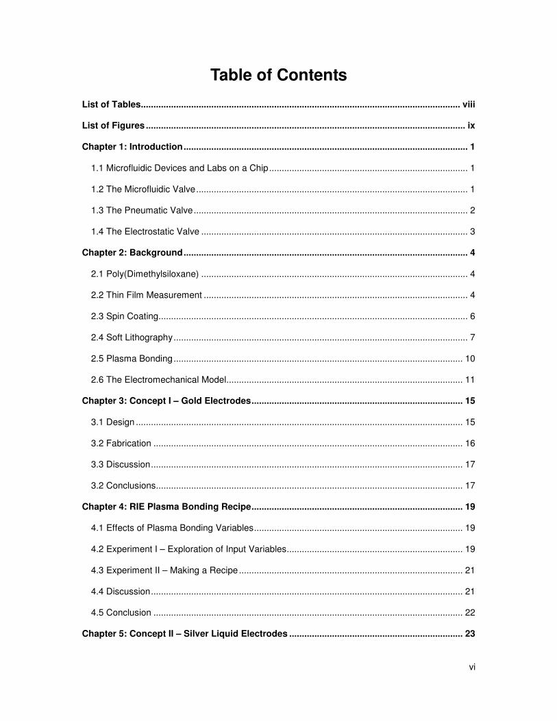
Table of Contents
List of Tables............................................................................................................................... viii
List of Figures ............................................................................................................................... ix
Chapter 1: Introduction................................................................................................................. 1
1.1 Microfluidic Devices and Labs on a Chip............................................................................... 1
1.2 The Microfluidic Valve............................................................................................................ 1
1.3 The Pneumatic Valve............................................................................................................. 2
1.4 The Electrostatic Valve .......................................................................................................... 3
Chapter 2: Background................................................................................................................. 4
2.1 Poly(Dimethylsiloxane) .......................................................................................................... 4
2.2 Thin Film Measurement ......................................................................................................... 4
2.3 Spin Coating........................................................................................................................... 6
2.4 Soft Lithography..................................................................................................................... 7
2.5 Plasma Bonding................................................................................................................... 10
2.6 The Electromechanical Model.............................................................................................. 11
Chapter 3: Concept I – Gold Electrodes.................................................................................... 15
3.1 Design .................................................................................................................................. 15
3.2 Fabrication ........................................................................................................................... 16
3.3 Discussion............................................................................................................................ 17
3.2 Conclusions.......................................................................................................................... 17
Chapter 4: RIE Plasma Bonding Recipe.................................................................................... 19
4.1 Effects of Plasma Bonding Variables................................................................................... 19
4.2 Experiment I – Exploration of Input Variables...................................................................... 19
4.3 Experiment II – Making a Recipe ......................................................................................... 21
4.4 Discussion............................................................................................................................ 21
4.5 Conclusion ........................................................................................................................... 22
Chapter 5: Concept II – Silver Liquid Electrodes ..................................................................... 23
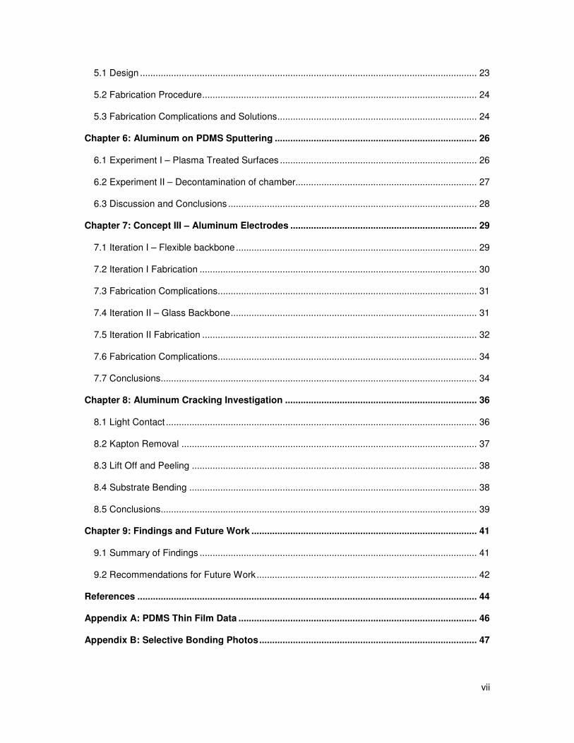
Page 7
vii
5.1 Design .................................................................................................................................. 23
5.2 Fabrication Procedure.......................................................................................................... 24
5.3 Fabrication Complications and Solutions............................................................................. 24
Chapter 6: Aluminum on PDMS Sputtering .............................................................................. 26
6.1 Experiment I – Plasma Treated Surfaces ............................................................................ 26
6.2 Experiment II – Decontamination of chamber...................................................................... 27
6.3 Discussion and Conclusions ................................................................................................ 28
Chapter 7: Concept III – Aluminum Electrodes ........................................................................ 29
7.1 Iteration I – Flexible backbone............................................................................................. 29
7.2 Iteration I Fabrication ........................................................................................................... 30
7.3 Fabrication Complications.................................................................................................... 31
7.4 Iteration II – Glass Backbone............................................................................................... 31
7.5 Iteration II Fabrication .......................................................................................................... 32
7.6 Fabrication Complications.................................................................................................... 34
7.7 Conclusions.......................................................................................................................... 34
Chapter 8: Aluminum Cracking Investigation .......................................................................... 36
8.1 Light Contact ........................................................................................................................ 36
8.2 Kapton Removal .................................................................................................................. 37
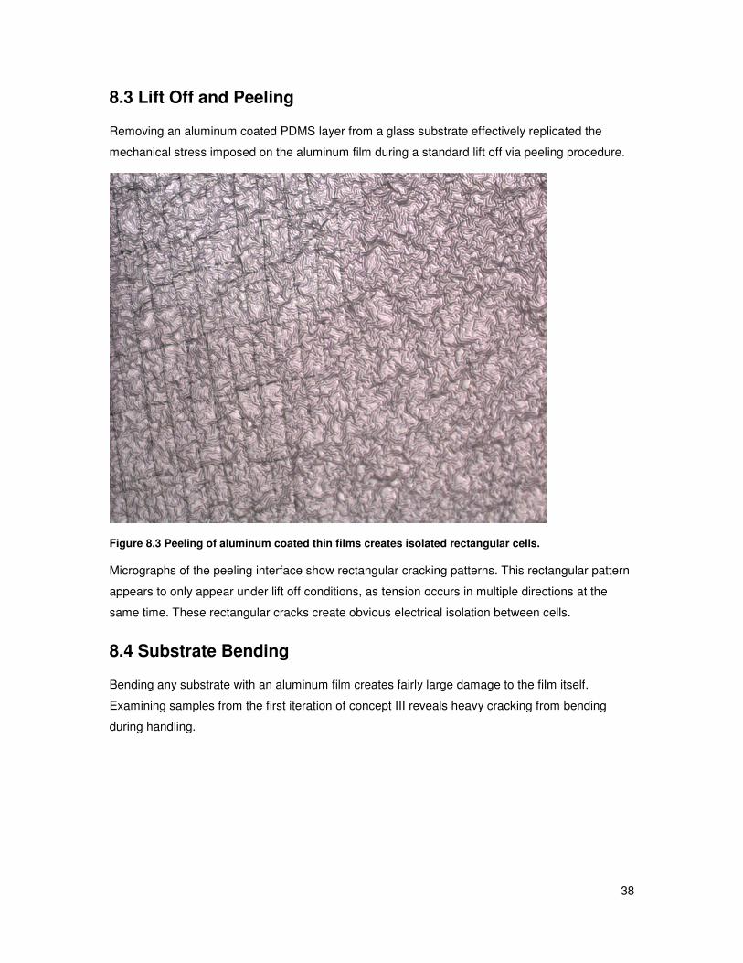
8.3 Lift Off and Peeling .............................................................................................................. 38
8.4 Substrate Bending ............................................................................................................... 38
8.5 Conclusions.......................................................................................................................... 39
Chapter 9: Findings and Future Work ....................................................................................... 41
9.1 Summary of Findings ........................................................................................................... 41
9.2 Recommendations for Future Work..................................................................................... 42
References ................................................................................................................................... 44
Appendix A: PDMS Thin Film Data ............................................................................................ 46
Appendix B: Selective Bonding Photos.................................................................................... 47
Page 8
viii
List of Tables
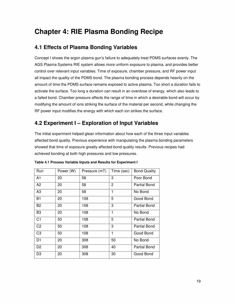
Table 4.1 Process Variable Inputs and Results for Experiment I ........................................... 19
Table 4.2 Time Inputs and Bond Quality Results of Experiment II......................................... 21
Page 9
ix
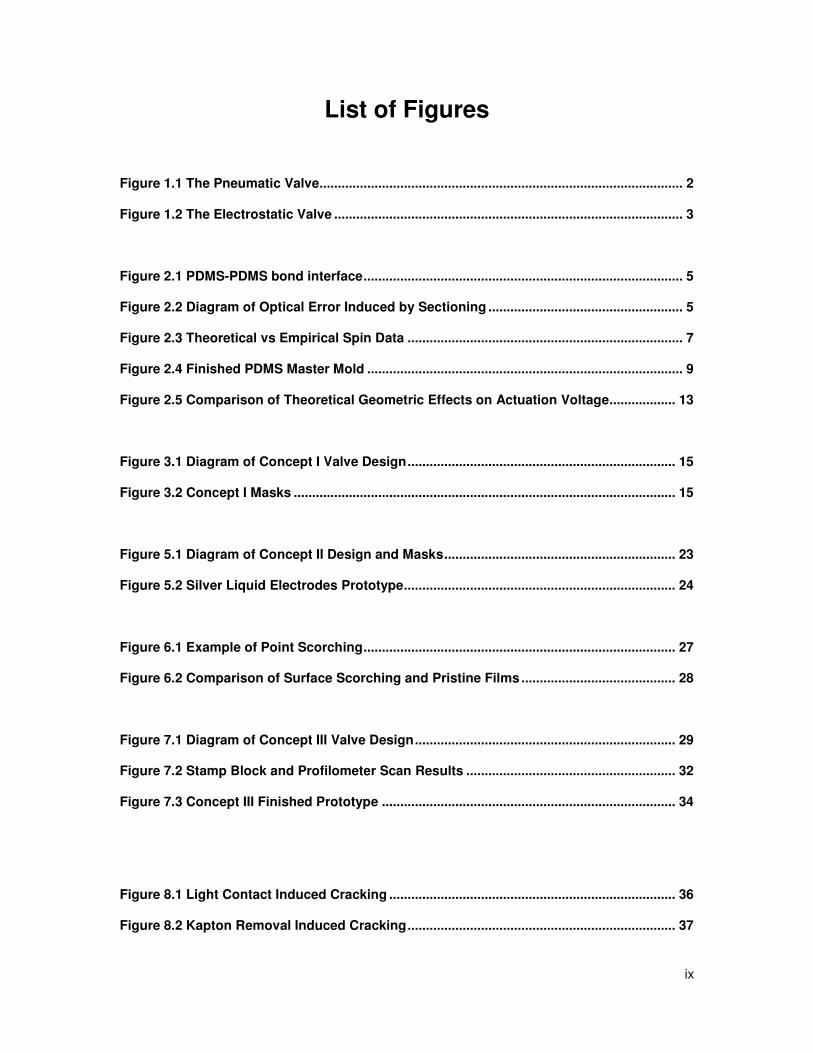
List of Figures
Figure 1.1 The Pneumatic Valve................................................................................................... 2
Figure 1.2 The Electrostatic Valve ............................................................................................... 3
Figure 2.1 PDMS-PDMS bond interface....................................................................................... 5
Figure 2.2 Diagram of Optical Error Induced by Sectioning ..................................................... 5
Figure 2.3 Theoretical vs Empirical Spin Data ........................................................................... 7
Figure 2.4 Finished PDMS Master Mold ...................................................................................... 9
Figure 2.5 Comparison of Theoretical Geometric Effects on Actuation Voltage.................. 13
Figure 3.1 Diagram of Concept I Valve Design......................................................................... 15
Figure 3.2 Concept I Masks ........................................................................................................ 15
Figure 5.1 Diagram of Concept II Design and Masks............................................................... 23
Figure 5.2 Silver Liquid Electrodes Prototype.......................................................................... 24
Figure 6.1 Example of Point Scorching..................................................................................... 27
Figure 6.2 Comparison of Surface Scorching and Pristine Films .......................................... 28
Figure 7.1 Diagram of Concept III Valve Design....................................................................... 29
Figure 7.2 Stamp Block and Profilometer Scan Results ......................................................... 32
Figure 7.3 Concept III Finished Prototype ................................................................................ 34
Figure 8.1 Light Contact Induced Cracking .............................................................................. 36
Figure 8.2 Kapton Removal Induced Cracking......................................................................... 37
Page 10
x
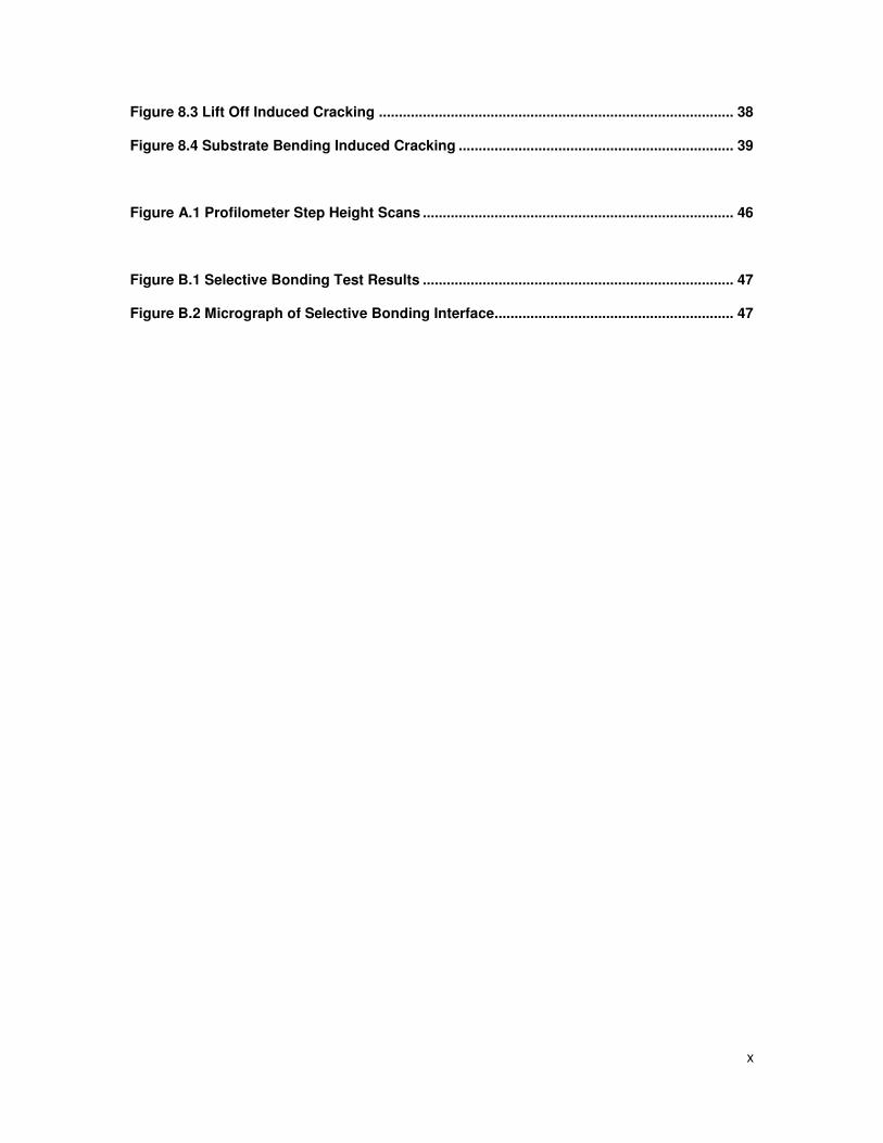
Figure 8.3 Lift Off Induced Cracking ......................................................................................... 38
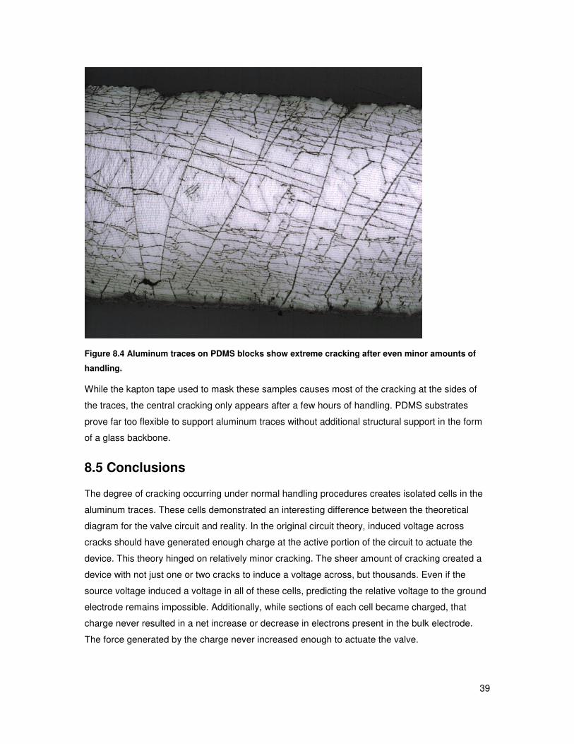
Figure 8.4 Substrate Bending Induced Cracking ..................................................................... 39
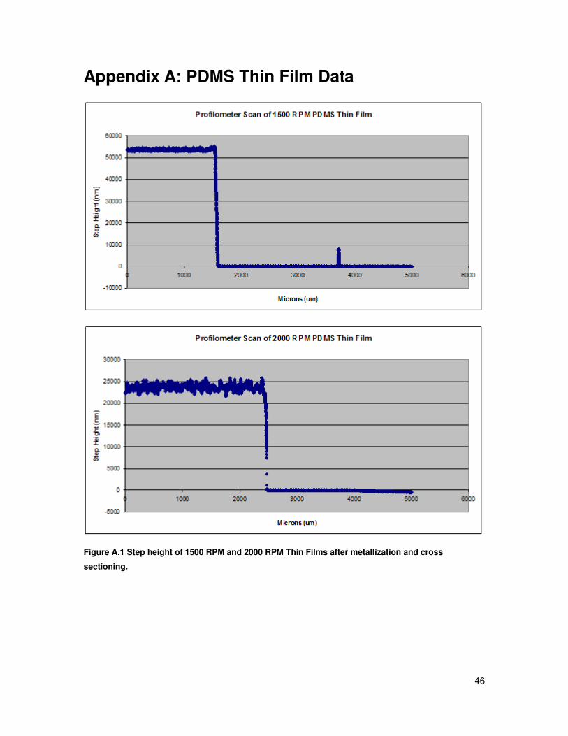
Figure A.1 Profilometer Step Height Scans .............................................................................. 46
Figure B.1 Selective Bonding Test Results .............................................................................. 47
Figure B.2 Micrograph of Selective Bonding Interface............................................................ 47
Page 11
1
Chapter 1: Introduction
1.1 Microfluidic Devices and Labs on a Chip
Microfluidic systems attempt to significantly increase the efficiency and control of chemical and
biological processes by shrinking reactions down to microscale dimensions. [1, 2] Microfluidic
devices can mix chemicals, capture individual cells, perform electrophoresis, separate DNA, and
in general perform many of the functions traditionally requiring complex lab setups. These
microscale devices require far less space and support structure than their large scale
counterparts. The active area of a microfluidic device usually spans less than 100 mm x 100 mm.
A network of microfluidic channels, valves, mixers, pumps, and other structures within the active
area accomplish the task of that particular device at a fraction of the size of a comparable
laboratory system. [3-8]
This small size creates a unique opportunity for researchers. Fabricating a testing setup on a
microfluidic platform theoretically allows for extremely portable and highly accurate testing
devices. Such a lab-on-a-chip would allow on site biological and chemical testing and reduce the
turnaround for test results significantly. [9]
1.2 The Microfluidic Valve
A microfluidic device consists of a series of channels that convey various fluids to different
components of a microfluidic chip. Microfluidic valves direct flow through fluid channels in even
the simplest devices, making them the most common form of microfluidic structure. Typical
prototype device valves use simple pneumatic or hydraulic pressure to deflect a
Poly(Dimethylsiloxane) (PDMS) membrane, closing a channel within various substrates. [10, 11,
12] The external power sources required to power pneumatic and hydraulic valves creates a
barrier to lab-on-a-chip design. Large external pressure sources such as syringe pumps require
large amounts of on-site power and storage space. A typical syringe pump weighs at least 2 kg
and takes up at least twice as much space as the device it powers. Laboratory syringe pumps
can require over 10 W of power to drive the syringe. [13] Each individually activated valve
requires its own syringe pump, and each syringe pump requires a channel leading to the valves it
actuates. These channels require a huge amount of space on a microfluidic device, and add at
least one additional layer of channel structures to a device. These factors severely limit the
complexity of a device using pneumatic systems.
The electrostatic valve can theoretically nullify these problems. A single electronic microchip can
control hundreds of electrostatic valves in the same manner a computer CPU controls billions of
transistors. While electrostatic valves require slightly higher voltages than syringe pumps, the
Page 12
2
capacitive nature of the circuits keeps current flow and thus power use to a minimum. The
controller can also theoretically require a single power source with enough voltage to drive the
electrostatic devices, making electrostatic valves a much more attractive choice for truly complex
lab-on-a-chip devices. Electrical traces take up far less volume than pneumatic source channels
and do not compromise the structural integrity of the device to the same degree. An electrostatic
valve actually becomes more efficient with further miniaturization on the Z axis. A thinner
channel’s electrodes rest closer together, reducing the voltage necessary to actuate the device.
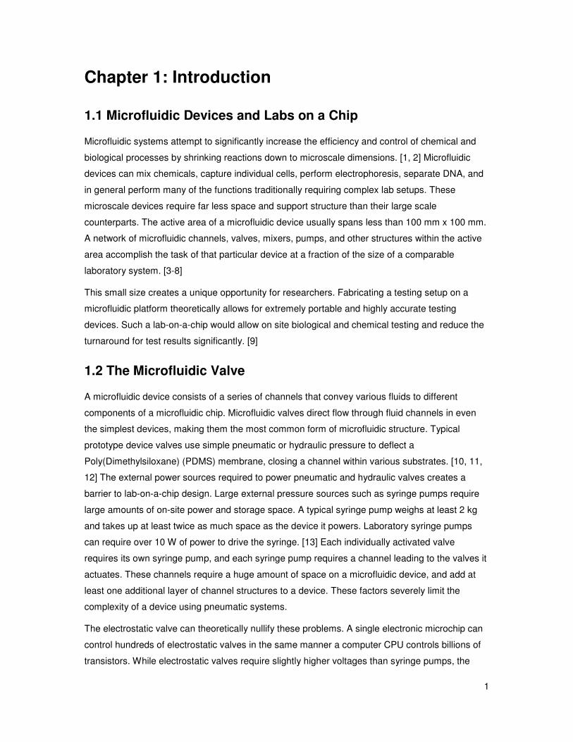
1.3 The Pneumatic Valve
Figure 1.1 Above: A basic pneumatically actuated microfluidic valve design. Below: Behavior of thin
membrane after pressurization of upper channel.
The key components of the pneumatic membrane valve most commonly used in microfluidic
prototypes provide a starting point for modifying the valve design to use electrostatic actuation.
[14] The typical pneumatic valve consists of a channel molded into a PDMS substrate and
capped by a second, thin membrane of PDMS bonded to the open side of the channel. This
assembly then bonds to a third layer containing a second channel which provides a conduit for
pneumatic pressure. After completion, auxiliary devices pressurize the upper channel, deflecting
the membrane until it squeezes the lower channel closed and prevents fluid flow.
Page 13
3
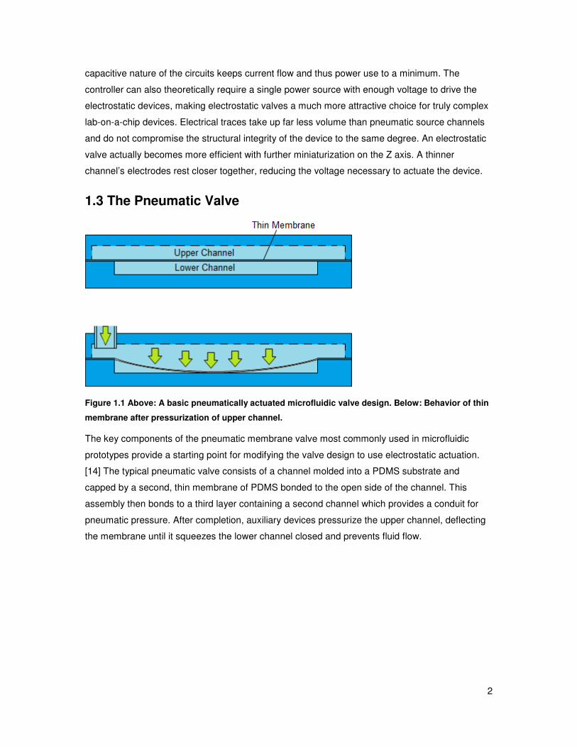
1.4 The Electrostatic Valve
Figure 1.2 Above: A basic electrostatically actuated microfluidic valve design. Below: Behavior of
thin membrane after application of driving voltage.
Theoretically, using electrostatically actuated valves in place of the traditional pneumatically
actuated valve reduces the number and size of auxiliary devices required to power the device.
Electrostatic force replaces pneumatic force in an electrostatic valve. Instead of an upper and
lower channel separated by a thin membrane, two electrodes fabricated into the upper and lower
walls of the channel become attracted by electrostatic forces generated by an applied voltage.
The electrostatic attraction deflects the membrane and closes the fluid channel in a manner
similar to the way the lower channel in a pneumatic valve closes.
The challenge in creating an electrostatic valve lies in fabrication. The question of how best to
design not only the valve itself but the step by step process which creates it leads to several
roadblocks. Metals typically do not bond to PDMS, making electrode fabrication extremely
difficult.
Additionally, the ideal electrostatic valve maintains an extremely low aspect ratio. The thinner the
channel, and the wider or longer the electrodes, the more force generated. However, too low an
aspect ratio can lead to PDMS channel collapse which can destroy the device.
Page 14
4
Chapter 2: Background
2.1 Poly(Dimethylsiloxane)
Microfluidic systems research typically uses poly(dimethylsiloxane) (PDMS) as the primary
substrate material of many prototype devices. These PDMS substrates possess many desirable
qualities for use in microfluidic devices, including high flexibility, low chemical reactivity, high
formability via soft lithography, and the ability to seal to other substrates via plasma bonding. [11]
PDMS manufacturers ship the material in two parts: a base and a catalyst. Mixing the base and
catalyst at a 10:1 ratio begins reactions that will crosslink the liquid polymer, eventually resulting
in a solid elastomeric material. [15] Following the mixing, the curing PDMS requires vacuum
treatment to remove air bubbles in the liquid. After removing the air the liquid PDMS can form into
nearly any desired shape via casting. At room temperature, the curing reaction takes 1-2 days to
complete. However, by elevating the temperature of the curing environment the process speeds
up immensely. At 75 ºC the process requires less than 45 minutes, and at 130 ºC the process can
take as little as 20 minutes. Higher temperatures during curing leave a small amount of stress in
the PDMS proportional to the thermal contraction that occurs on cooling to room temperature.
Cured PDMS has a very low elastic modulus estimated at 750 kPa. [16] This low elastic modulus
makes PDMS an ideal material for thin membrane valves. Very low amounts of pressure can
close a PDMS membrane valve. The elastomeric nature of PDMS allows it to elastically stretch
many times its equilibrium length before rupturing, stretching to cut off most or all of a channel.
Most chemicals have no effect on fully cured PDMS. The nonpolar nature of PDMS gives it a
hydrophobic surface and makes it impermeable to water. A cured substrate becomes all but
impervious to chemical attack from anything other than organic solvents. Exposure to organic
solvent solutions results in temporary swelling of the PDMS substrate as the solvent diffuses into
the material. [17] The swelling subsides as the solvent evaporates and diffuses back out of the
PDMS.
2.2 Thin Film Measurement
Thin film measurement presents one of the largest difficulties in designing a microfluidic device.
Typical methods for measuring thin films such as profilometry and multiwavelength reflection
spectroscopy cannot function with PDMS thin films. PDMS films rarely achieve thicknesses of
less than 5 µm. The clean room’s multiwavelength reflection spectroscopy system cannot analyze
films that thick due to the bandwidth limitations of the light source and generally poor parameters
for PDMS. [18] Profilometer tips stick to the extremely soft surface of PDMS, which can cause
thousands of dollars in damage by breaking a profilometer tip as it travels across the surface of
Page 15
5
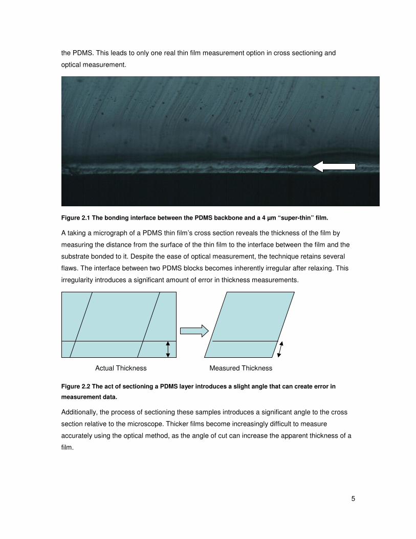
the PDMS. This leads to only one real thin film measurement option in cross sectioning and
optical measurement.
Figure 2.1 The bonding interface between the PDMS backbone and a 4 µm “super-thin” film.
A taking a micrograph of a PDMS thin film’s cross section reveals the thickness of the film by
measuring the distance from the surface of the thin film to the interface between the film and the
substrate bonded to it. Despite the ease of optical measurement, the technique retains several
flaws. The interface between two PDMS blocks becomes inherently irregular after relaxing. This
irregularity introduces a significant amount of error in thickness measurements.
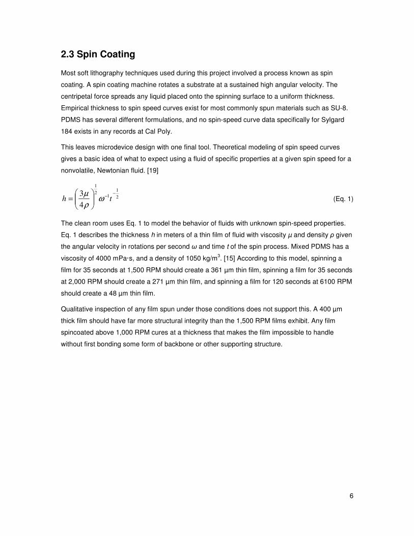
Figure 2.2 The act of sectioning a PDMS layer introduces a slight angle that can create error in
measurement data.
Additionally, the process of sectioning these samples introduces a significant angle to the cross
section relative to the microscope. Thicker films become increasingly difficult to measure
accurately using the optical method, as the angle of cut can increase the apparent thickness of a
film.
Actual Thickness Measured Thickness
Page 16
6
2.3 Spin Coating
Most soft lithography techniques used during this project involved a process known as spin
coating. A spin coating machine rotates a substrate at a sustained high angular velocity. The
centripetal force spreads any liquid placed onto the spinning surface to a uniform thickness.
Empirical thickness to spin speed curves exist for most commonly spun materials such as SU-8.
PDMS has several different formulations, and no spin-speed curve data specifically for Sylgard
184 exists in any records at Cal Poly.
This leaves microdevice design with one final tool. Theoretical modeling of spin speed curves
gives a basic idea of what to expect using a fluid of specific properties at a given spin speed for a
nonvolatile, Newtonian fluid. [19]
2
1
12
1
4
3 −−
= th ω
ρ
µ (Eq. 1)
The clean room uses Eq. 1 to model the behavior of fluids with unknown spin-speed properties.
Eq. 1 describes the thickness h in meters of a thin film of fluid with viscosity µ and density ρ given
the angular velocity in rotations per second ω and time t of the spin process. Mixed PDMS has a
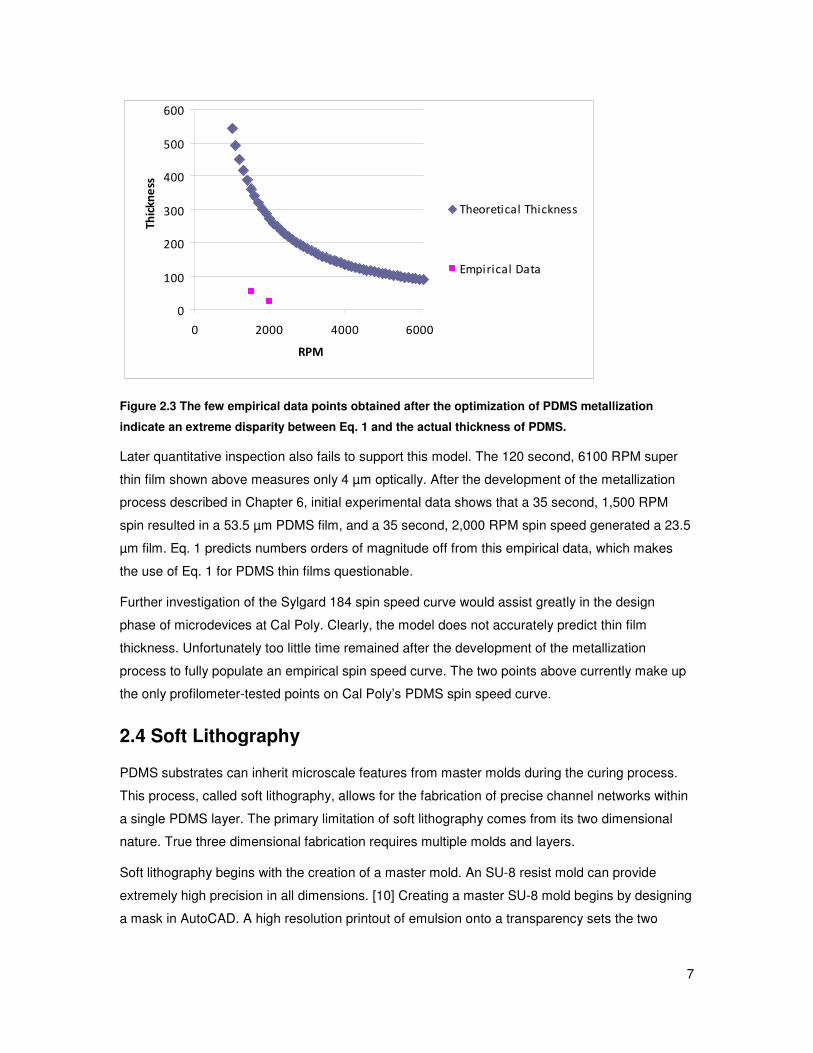
viscosity of 4000 mPa·s, and a density of 1050 kg/m3. [15] According to this model, spinning a
film for 35 seconds at 1,500 RPM should create a 361 µm thin film, spinning a film for 35 seconds
at 2,000 RPM should create a 271 µm thin film, and spinning a film for 120 seconds at 6100 RPM
should create a 48 µm thin film.
Qualitative inspection of any film spun under those conditions does not support this. A 400 µm
thick film should have far more structural integrity than the 1,500 RPM films exhibit. Any film
spincoated above 1,000 RPM cures at a thickness that makes the film impossible to handle
without first bonding some form of backbone or other supporting structure.
Page 17
7
0
100
200
300
400
500
600
0 2000 4000 6000
RPM
Thickness
Theoretical Thickness
Empirical Data
Figure 2.3 The few empirical data points obtained after the optimization of PDMS metallization
indicate an extreme disparity between Eq. 1 and the actual thickness of PDMS.
Later quantitative inspection also fails to support this model. The 120 second, 6100 RPM super
thin film shown above measures only 4 µm optically. After the development of the metallization
process described in Chapter 6, initial experimental data shows that a 35 second, 1,500 RPM
spin resulted in a 53.5 µm PDMS film, and a 35 second, 2,000 RPM spin speed generated a 23.5
µm film. Eq. 1 predicts numbers orders of magnitude off from this empirical data, which makes
the use of Eq. 1 for PDMS thin films questionable.
Further investigation of the Sylgard 184 spin speed curve would assist greatly in the design
phase of microdevices at Cal Poly. Clearly, the model does not accurately predict thin film
thickness. Unfortunately too little time remained after the development of the metallization
process to fully populate an empirical spin speed curve. The two points above currently make up
the only profilometer-tested points on Cal Poly’s PDMS spin speed curve.
2.4 Soft Lithography
PDMS substrates can inherit microscale features from master molds during the curing process.
This process, called soft lithography, allows for the fabrication of precise channel networks within
a single PDMS layer. The primary limitation of soft lithography comes from its two dimensional
nature. True three dimensional fabrication requires multiple molds and layers.
Soft lithography begins with the creation of a master mold. An SU-8 resist mold can provide
extremely high precision in all dimensions. [10] Creating a master SU-8 mold begins by designing
a mask in AutoCAD. A high resolution printout of emulsion onto a transparency sets the two
Page 18
8
dimensional pattern of each feature. At Cal Poly, typical masks with no features under 100µm use
5,000 DPI. Features under 15 µm typically require 10,000 DPI.
After preparing the mask, a general fabrication procedure generates a master mold. Process
variables such as spin speed and bake time remain dependant on the desired mold thickness.
Exposure to water during the development creates an extremely thick white residue and
effectively destroys the mold. The following values correspond to a typical 40 µm tall mold. [20]
1. Clean a silicon wafer with a Piranha bath followed by a BOE bath
2. Dehydrate bake the wafer at 150 ºC for 2 minutes
3. Transfer to spin coater
4. Pour a small amount of SU-8 2050 onto the wafer
5. Spin wafer at 4000 RPM for 30 seconds
6. Bake wafer at 65 ºC for 90 seconds
7. Bake at 95 ºC for 6 minutes
8. Transfer wafer to aligner and apply mask directly to wafer.
9. Cover wafer with 5 in x 5 in glass plate and 5 in x 5 in UV filter plate
10. Expose wafer to UV lamp for 140–180 seconds
11. Bake wafer at 65 ºC for 1 minute
12. Bake at 95 ºC for 6 minutes
13. Develop resist in SU-8 developer
14. Rinse with isopropyl alcohol
15. Hard bake at 130 ºC for 2 minutes
16. Inspect mold for defects
A more advanced method of mold fabrication uses multiple SU-8 applications to fine tune the
height. This technique allows creation of molds with features greater than 250 µm tall, or features
beyond the maximum height tolerances of SU-8 2007 and 2050. The process flow changes
during the spincoating process. The following process creates a pattern greater than 250 microns
tall.
1. Clean a silicon wafer with a Piranha bath followed by a BOE bath
2. Dehydrate bake the wafer at 150 ºC for 2 minutes
3. Dehydrate bake wafer at 150 ºC for 2 minutes
4. Transfer to spin coater
5. Spin on SU-8 2050 at 1250 RPM for 30 seconds
6. Bake wafer at 65 ºC for 5 minutes
7. Bake at 95 ºC for 30 minutes
8. Repeat steps 20-22 varying spin speed and bake times as necessary
9. Transfer wafer to aligner and apply mask directly to wafer.
Page 19
9
10. Cover wafer with 5 in x 5 in glass plate and 5 in x 5 in UV filter plate
11. Expose wafer to UV lamp for 8 minutes
12. Bake wafer at 65 ºC for 5 minutes
13. Bake at 95 ºC for 15 minutes
14. Develop resist in SU-8 developer
15. Rinse with isopropyl alcohol
16. Hard bake at 130 ºC for 2 minutes
17. Inspect mold for defects
Multilayer patterning techniques can also help bridge the gap between the low viscosity 2007
formulation and the high viscosity 2050 formulations of SU-8 which the clean room currently uses.
Due to the low viscosity of SU-8 2007 obtaining features taller than 12-13 µm becomes difficult in
one spin pass. However, stacking multiple layers of 2007 using the multilayer process can
generate taller molds in 7-12 µm increments simply by varying the spin speed and soft bake
times of each incremental layer. The SU-8 can expose as a single unit after application and soft
baking of the individual layers.
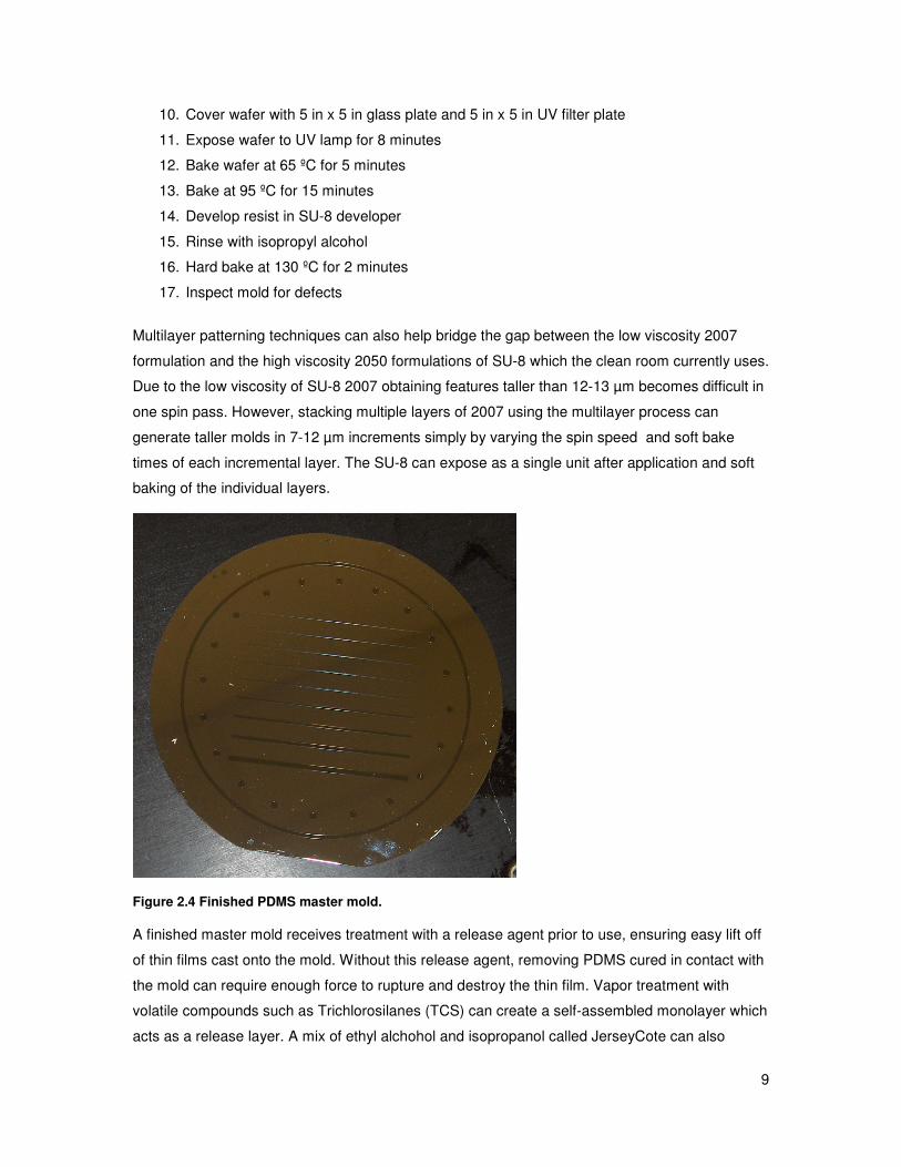
Figure 2.4 Finished PDMS master mold.
A finished master mold receives treatment with a release agent prior to use, ensuring easy lift off
of thin films cast onto the mold. Without this release agent, removing PDMS cured in contact with
the mold can require enough force to rupture and destroy the thin film. Vapor treatment with
volatile compounds such as Trichlorosilanes (TCS) can create a self-assembled monolayer which
acts as a release layer. A mix of ethyl alchohol and isopropanol called JerseyCote can also
Page 20
10
create a release layer when spun onto a wafer at 3000 RPM for 60 seconds. The Cal Poly clean
room has effectively phased out TCS use in favor of the less dangerous and time consuming
JerseyCote release agent.
A complete master mold can imprint multiple PDMS layers. Imprinting a layer requires
spincoating liquid PDMS to the desired thickness over the mold, curing the PDMS, and lifting off
the layer. Thin film layers typically need additional support during the lift off phase, using a
backbone bonded to the film prior to removal from the mold.
2.5 Plasma Bonding
The key benefit to using PDMS as a substrate material lies in the ability of PDMS to bond to itself
easily through relatively simple plasma treatments. The plasma bonding process creates a bond
with a virtually undetectable interface which possesses material properties nearly identical to the
bulk material. In essence, the surfaces of the two PDMS pieces cease to exist and a single
macroscopically continuous block remains. [10]
This property has advantages when creating three dimensional structures. The ability to create a
single object by stacking multiple layers on top of one another allows for complex, sealed channel
networks on the micro and meso scale. These layers combine into an effectively continuous
structure allowing remarkably complex designs with little to no leaks. The multilayer system also
allows channels to cross other channels by routing over or under a channel. By manipulating
these benefits, many features of piping systems can occur at the micro level.
PDMS can also bond to other substrate materials such as SiO2 and Si through the same method.
Glass microscope slides make stable and relatively inexpensive device platforms for many
devices. Typically these substrates see use in applications requiring a degree of rigidity.
To generate a plasma bond, PDMS substrates first need preparation. Each surface has tape
attached and removed to clean the surface of any particulate matter such as dust or cloth
fragments. Once cleaned, both substrates enter the vacuum chamber of a Rapid Ion Etching
(RIE) machine. The RIE creates oxygen plasma in a low vacuum environment. Exposure to
oxygen plasma replaces methyl groups on the surface of the substrate with an oxygen molecule.
These oxygen molecules have dangling bonds. Upon venting the vacuum chamber, the hydrogen
in the atmosphere bonds with the oxygen groups creating a large number of hydroxide groups on
the surface of the substrate. The substrates require assembly within 10 minutes or the surfaces
will relax too far to bond. Once assembled, the substrates bake within an oven at 65 to 75 ºC for
at least 30 minutes. During this time, the hydroxide groups on the surfaces allow the surfaces to
bond together via condensation, effectively removing the surface entirely.
Page 21
11
An argon plasma gun can also treat a PDMS surface. Plasma gun treatments require less lab
space and less expensive equipment. However, using a plasma gun decreases control over
exposure variables significantly, and can cause problems with sealing.
Underexposure or overexposure to plasma can thwart the bonding process by either failing to
create enough hydroxide groups on the surface or causing too much damage to the surface to
allow for bonding. In addition, PDMS begins to relax immediately after removing the treated
surfaces from the plasma. The surfaces must come in contact and begin bonding within minutes
of shutting off the oxygen plasma or the bond will fail. This severely restricts the alignment
between layers.
Another concern during plasma bonding comes in the form of interchannel leaking. Channels
placed too closely together in a layer may not have enough bonded area between them to hold
back the pressures within the channel, generating ruptures and leaks. These cases generally
occur due to poor or partial bonds. In some cases, a bond removed from an oven too early can
fail to fully cure and rupture during operation as well. Channels closer than 5000 µm separation
can see fairly extreme interchannel leaking, especially with smaller channels which require more
pressure to push the initial fluid/PDMS contact line fully through the device.
The most common form of bonding failure comes from channel collapse. Thin membranes
covering channels can collapse during the bonding step and become permanently sealed to the
floor of the channel. This phenomenon usually occurs only in channels with a greater than 10:1
width to depth ratio, though extremely wide channels greater than 500 µm become more prone to
collapse as the width increases.
Plasma treatment can also generate temporary hydrophilic surfaces. The hydroxide groups
polarize the surface molecules and create a surface layer of hydrophilic material. Just as in
plasma bonding, the surfaces relax over time to their original hydrophobic state.
2.6 The Electromechanical Model
Deriving a general model of the electromechanical behavior of an electrostatic valve provides a
convenient design tool for determining the appropriate dimensions for a prototype valve. This
electromechanical model incorporates geometric, mechanical, electrical, and material factors into
a calculation resulting in the theoretical voltage required to fully close a valve of the given
parameters.
The derivation begins with the relationship between an applied voltage across a parallel plate
capacitor and its resulting force. [21]
2
2V
d
CF = (2)
Page 22
12
The applied voltage V greatly affects the force output of an electrostatic device. The sum of the
thickness of all components between the electrodes results in the distance d between the plates.
hHd 2+= (3)
Where H describes the height of the channel, and h describes the thickness of each wall
membrane. The capacitance C expands to:
fluidwallstotal CCC += 2 (4)
h
AC wall
walls
εε 0= (5)
H
AC
fluid
fluid
εε 0= (6)
The relative permittivities εfluid and εwall describe the material contribution to the capacitance.
Combining the area A with the force applied F results in a relationship between the applied
voltage, channel geometry, and the pressure generated by the electrostatic attraction.
2
)2(2
2
VhH
Hh
A
FP
fluidowallso
+
+
==
εεεε
(7)
Some rearrangement via algebra obtains the equation for the voltage required to apply a specific
pressure to the valve membrane.
+
+=
Hh
hHPV
fluidowallsoεεεε2
)2(2 (8)
Reasearch done by Kartalov et al. has constructed an empirical model for the pressure required
to push down a rectangular valve membrane. [22]
+
−++
+
+=
44
333
22
211
5
16
3
164
11
3
161ln
LW
HhHhH
LW
HEP (9)
Where E represents the elastic modulus of the membrane material, W represents the width of the
membrane, and L represents the length of the membrane. Using both Eq. 8 and 9 results in the
theoretical voltage required to actuate a rectangular electrostatic valve of specific geometric and
material construction.
Page 23
13
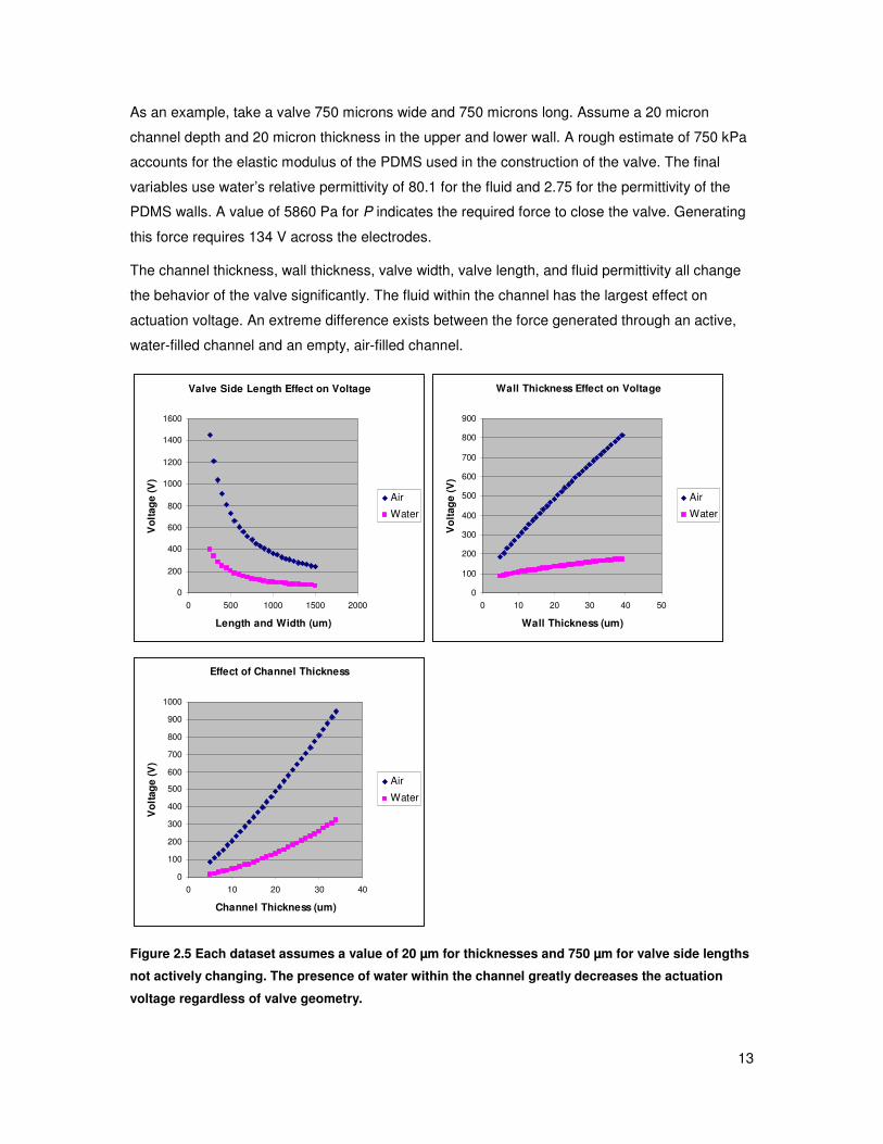
As an example, take a valve 750 microns wide and 750 microns long. Assume a 20 micron
channel depth and 20 micron thickness in the upper and lower wall. A rough estimate of 750 kPa
accounts for the elastic modulus of the PDMS used in the construction of the valve. The final
variables use water’s relative permittivity of 80.1 for the fluid and 2.75 for the permittivity of the
PDMS walls. A value of 5860 Pa for P indicates the required force to close the valve. Generating
this force requires 134 V across the electrodes.
The channel thickness, wall thickness, valve width, valve length, and fluid permittivity all change
the behavior of the valve significantly. The fluid within the channel has the largest effect on
actuation voltage. An extreme difference exists between the force generated through an active,
water-filled channel and an empty, air-filled channel.
Valve Side Length Effect on Voltage
0
200
400
600
800
1000
1200
1400
1600
0 500 1000 1500 2000
Length and Width (um)
Vo
ltag
e (
V)
Air
Water
Wall Thickness Effect on Voltage
0
100
200
300
400
500
600
700
800
900
0 10 20 30 40 50
Wall Thickness (um)
Vo
ltag
e (
V)
Air
Water
Effect of Channel Thickness
0
100
200
300
400
500
600
700
800
900
1000
0 10 20 30 40
Channel Thickness (um)
Vo
ltag
e (
V)
Air
Water
Figure 2.5 Each dataset assumes a value of 20 µm for thicknesses and 750 µm for valve side lengths
not actively changing. The presence of water within the channel greatly decreases the actuation
voltage regardless of valve geometry.
Page 24
14
Water’s relative permittivity of 80.1 greatly amplifies the electrostatic field. By comparison the
2.75 relative permittivity of PDMS becomes completely overwhelmed in the presence of water.
Specifically, the presence of water in the channel should allow much thicker walls between the
electrodes and the channel itself. Increasing the thickness of the channel greatly increases the
voltage required to actuate the device. The model also predicts severely increasing voltages for
valves widths and lengths under 500 µm.
Page 25
15
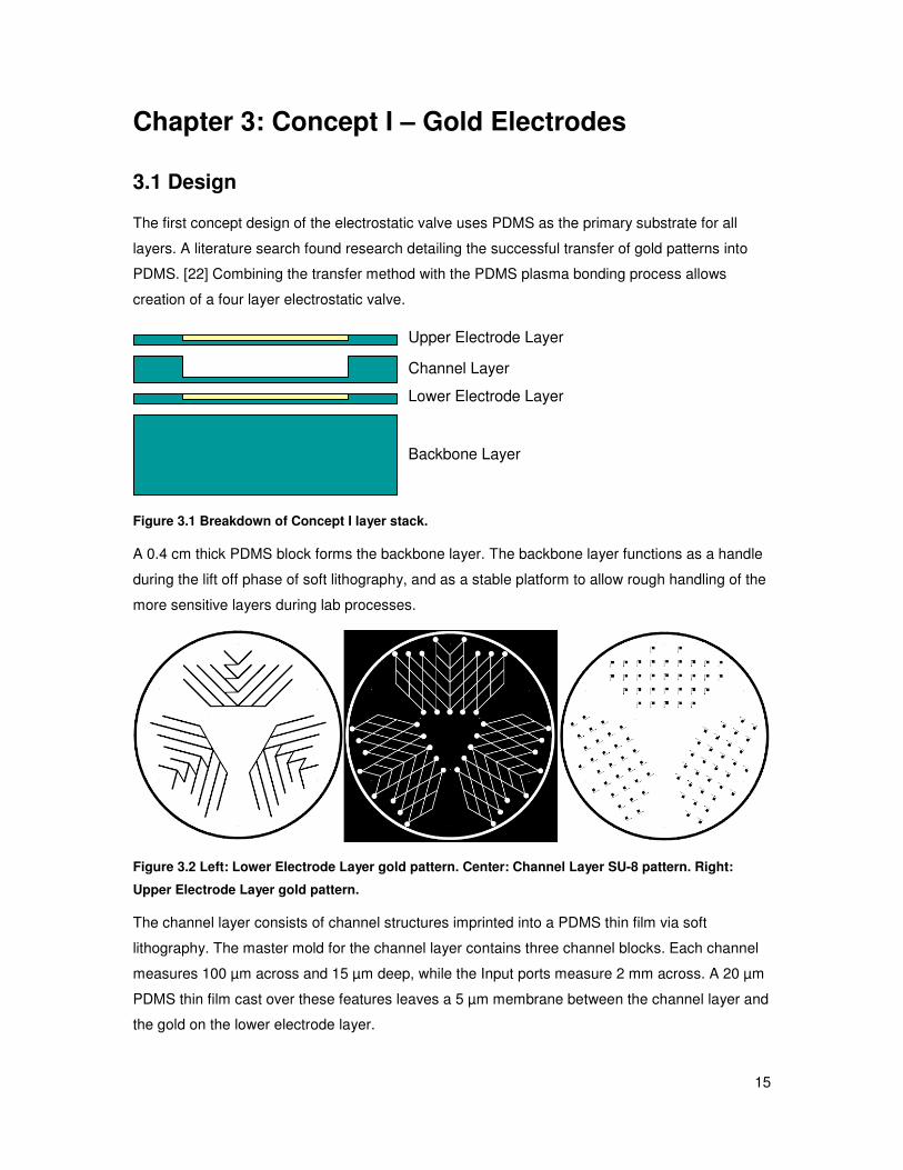
Chapter 3: Concept I – Gold Electrodes
3.1 Design
The first concept design of the electrostatic valve uses PDMS as the primary substrate for all
layers. A literature search found research detailing the successful transfer of gold patterns into
PDMS. [22] Combining the transfer method with the PDMS plasma bonding process allows
creation of a four layer electrostatic valve.
Figure 3.1 Breakdown of Concept I layer stack.
A 0.4 cm thick PDMS block forms the backbone layer. The backbone layer functions as a handle
during the lift off phase of soft lithography, and as a stable platform to allow rough handling of the
more sensitive layers during lab processes.
Figure 3.2 Left: Lower Electrode Layer gold pattern. Center: Channel Layer SU-8 pattern. Right:
Upper Electrode Layer gold pattern.
The channel layer consists of channel structures imprinted into a PDMS thin film via soft
lithography. The master mold for the channel layer contains three channel blocks. Each channel
measures 100 µm across and 15 µm deep, while the Input ports measure 2 mm across. A 20 µm
PDMS thin film cast over these features leaves a 5 µm membrane between the channel layer and
the gold on the lower electrode layer.
Backbone Layer
Lower Electrode Layer
Channel Layer
Upper Electrode Layer
Page 26
16
Both electrode layers contain 60 nm thick gold electrodes transferred into PDMS thin films. A
vapor treatment of 3-Mercaptopropyl Trimethoxysilane (MPT) over the gold surfaces creates a
self-assembled monolayer. This methoxy groups in MPT bond to the PDMS as it cures over the
monolayer, creating an adhesion layer between the gold and the 20 µm PDMS thin film, which
improves the quality of the transfer. The lower electrode design allows a single point of electrical
contact to ground the entire channel block.
Each prototype device contains 32 separate valves to ensure at least a few valves survive the
various fabrication steps. A network of fluid channels connects these valves, designed to require
a minimal amount input and output ports on the channel layer to reduce the amount of damage to
the upper electrode layer during testing.
3.2 Fabrication
Backbone Layer Fabrication Recipe
1. Mix 35 ml Sylgard 184 at a 10:1 base to catalyst ratio
2. Place mixture into vacuum chamber and degas for 10 minutes
3. Pour liquid PDMS into 6” petri dish
4. Cure PDMS in oven at 75 ºC for 45 minutes
Upper/Lower Electrode Layer Fabrication Recipe
1. Sputter gold onto wafer at 9 mTorr and 60 W for 1 minute
2. Spin on HMDS primer at 500 RPM for 30 seconds
3. Spin on positive photoresist at 3000 RPM for 30 seconds
4. Soft bake positive photoresist at 90 ºC for 1 minute
5. Expose positive photoresist for 16 seconds
6. Develop positive photoresist using CD-26
7. Etch gold using KI based gold etchant
8. Vapor treat surface with MPT
9. Vapor treat surface with TCS
10. Spin on 3 ml Sylgard 184 at 3000 RPM for 30 seconds
11. Cure PDMS in oven at 75 ºC for 45 minutes
Channel Layer Fabrication Recipe
1. Vapor treat channel layer master mold with TCS
2. Spin on 3 ml Sylgard 184 at 2000 RPM for 30 seconds
3. Cure PDMS in oven at 75 ºC for 45 minutes
Page 27
17
3.3 Discussion
Unfortunately, none of the devices ever fully survived the fabrication process. Multiple
complications arose during fabrication of the active layers.
Initial designs left the electrode layer PDMS thin films so thin they fell apart during bonding and lift
off. A decrease in spin speed to match the channel layer thickness solved this issue. In addition,
combining the backbone and lower electrode layer reinforced the lower electrode layer during lift
off.
The MPT adhesion layer failed to function properly. Two possibilities explain this phenomenon.
First, the TCS release agent and the MPT adhesion agent could interfere with one another. Both
the chemicals use the formation of a self-assembled monolayer via vapor treatment to change the
properties of the surface. The TCS and MPT directly conflict with one another for monolayer
formation. Second, the MPT could have failed to properly coat the gold traces.
Rearranging the process steps to expose the wafer to the TCS release agent prior to gold
sputtering resulted in PDMS tearing during release of the layer. Additionally, the reorganized
recipe continued to fail to fully transfer the gold films. Testing gold transfer with and without the
MPT confirmed the MPT had no effect on transfer quality. This suggested the MPT vapor
treatments failed to successfully coat the gold traces. MPT appears to require a vacuum
assistance to properly vaporize and create a SAM on the wafer. The clean room has no vacuum
chambers inside fume hoods, and the toxic nature of MPT precludes its use outside of a fume
hood.
A thin oxide coating on surface of the wafer substrate succeeded in releasing the gold from the
substrate without MPT adhesion layers. However, the gold thin film experienced severe
delamination problems during wet etch processes.
Finally, the complexity of the design worked against success. While multiple valves existed on
each block, the large blocks developed several leaks due to the uneven treatment from the
plasma gun. While one or two electrodes might survive a transfer intact, no corresponding
electrode ever survived to allow creation of a fully functional valve.
3.2 Conclusions
Concept I ruled out gold as an electrode material. The results of K.J. Lee et al. proved impossible
to reproduce with the equipment available. The cost of electronics grade gold precluded further
attempts at developing a method for full transfer.
Page 28
18
Concept I also revealed that extremely thin (<10 µm) PDMS layers do not possess enough
durability to reliably survive the lift off process. Additionally, concept I revealed the ineffectiveness
of complex device designs.
Page 29
19
Chapter 4: RIE Plasma Bonding Recipe
4.1 Effects of Plasma Bonding Variables
Concept I shows the argon plasma gun’s failure to adequately treat PDMS surfaces evenly. The
AGS Plasma Systems RIE system allows more uniform exposure to plasma, and provides better
control over relevant input variables. Time of exposure, chamber pressure, and RF power input
all impact the quality of the PDMS bond. The plasma bonding process depends heavily on the
amount of time the PDMS surface remains exposed to active plasma. Too short a duration fails to
activate the surface. Too long a duration can result in an overdose of energy, which also leads to
a failed bond. Chamber pressure affects the range of time in which a desirable bond will occur by
modifying the amount of ions striking the surface of the material per second, while changing the
RF power input modifies the energy with which each ion strikes the surface.
4.2 Experiment I – Exploration of Input Variables
The initial experiment helped glean information about how each of the three input variables
affected bond quality. Previous experience with manipulating the plasma bonding parameters
showed that time of exposure greatly affected bond quality results. Previous recipes had
achieved bonding at both high pressures and low pressures.
Table 4.1 Process Variable Inputs and Results for Experiment I
Run Power (W) Pressure (mT) Time (sec) Bond Quality
A1 20 58 3 Poor Bond
A2 20 58 2 Partial Bond
A3 20 58 1 No Bond
B1 20 108 5 Good Bond
B2 20 108 3 Partial Bond
B3 20 108 1 No Bond
C1 50 108 5 Partial Bond
C2 50 108 3 Partial Bond
C3 50 108 1 Good Bond
D1 20 308 50 No Bond
D2 20 308 40 Partial Bond
D3 20 308 30 Good Bond
Page 30
20
The experiment helped determine the effect of changes to pressure and power input on the time
required to create a strong and uniform bond. Each test involved two blocks of thermally cured
PDMS treated under specific pressure, power, and time conditions.
The experiment tested each of four different power and pressure combinations. Cal Poly does not
posess the necessary equipment to effectively test the strength of the bond. In lieu of quantitative
data, qualitative testing must suffice. Three criteria describe a “good bond”:
1. A complete bond, with no areas near edges which failed to bond.
2. The bond must withstand tearing across the interface, indicating the toughness of the bonded region to match or exceed the toughness of the bulk material.
3. The torn surface must give no visual indicator of where the interface between the two previous surfaces exists.
A “partial bond” complies with conditions two and three, but has areas where the bond failed to
take hold. Typically, these areas occur near edges of the two PDMS substrates. Partial bonding
can result from a lack or excess of plasma exposure. More extreme partial bonding issues occur
from dirt or other contamination present on the substrates during plasma treatment. Devices
which partially bond leak, causing cross channel contamination, and cannot properly function as
microfluidic devices.
“No bond” means a test in which no bond occurred at all. Both pieces separated from each other
without resistance. A no bond result indicates configurations that have too little or too much time
of exposure, and as a result have failed to activate the surface of the substrate.
The results of runs A1 through A3 at 20 W and 58 mT showed a lack of bonding at 1 sec and a
poor bond at 3 sec of exposure time. However, at 2 sec of exposure, the bond held strongly at
most of the interface, though the edges failed to bond in many places.
Runs B1 through B3 increased the pressure to 108 mT show a dramatic expansion of the window
in time of exposure values in which a strong bond can occur. A 3 sec treatment produced similar
results to run A2, while run B3 produced a good bond with a 5 sec treatment.
Runs C1 through C3 increased the power output to 50 W at 108 mT. The degradation in bond
quality indicates that increasing the power input may cause general bond degradation.
Runs D1 through D3 returned the power output to 20 W at 308 mT. Previous recipes achieved
successful bonds at timestamps greater than 30 seconds. The success of the 30 second
sample’s bond shows a much larger time window at the higher chamber pressure.
Page 31
21
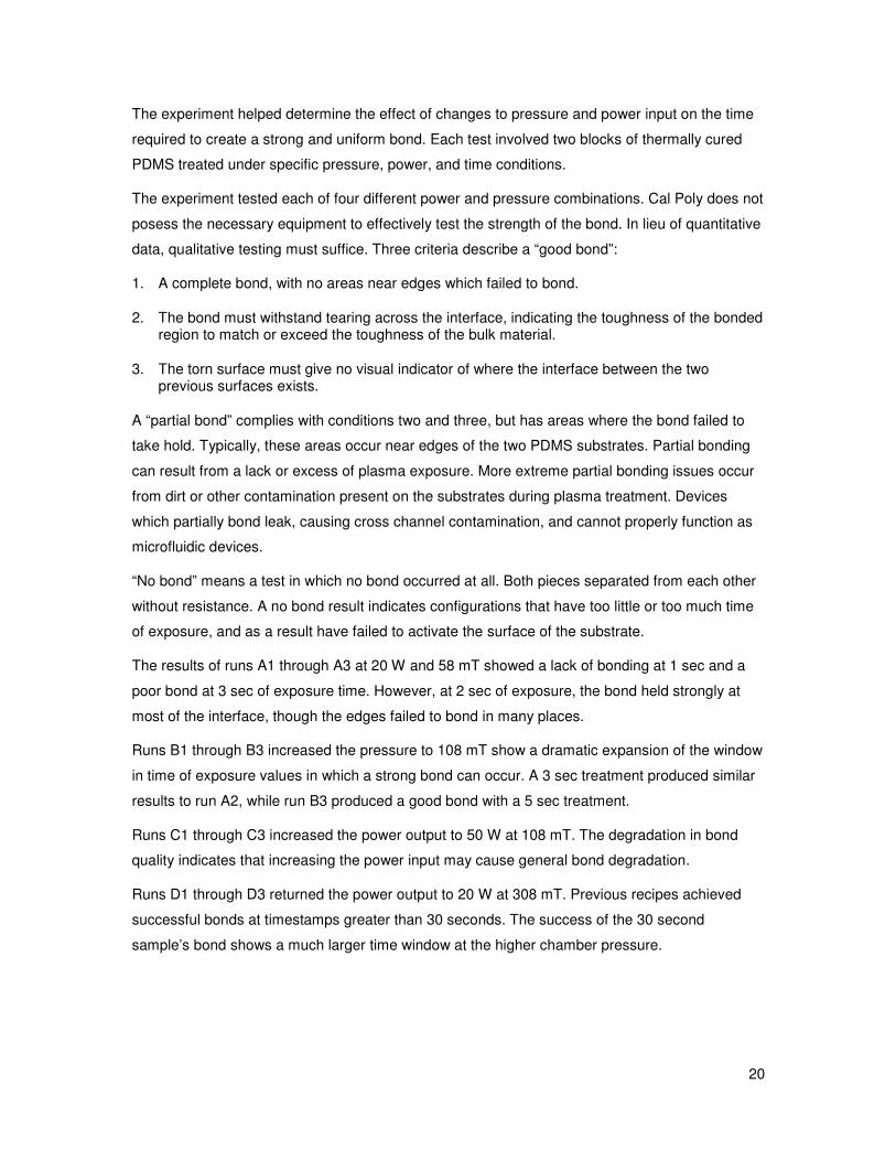
4.3 Experiment II – Making a Recipe
The second experiment used the information gleaned from experiment I to explore the time of
exposure window more effectively. All runs of this experiment took place at 20 W and 308 mT.
The previous experiment’s results indicated a lower power and higher pressure would extended
the time of exposure window to an interval in which more samples could better indicate which
times created optimal bonds.
Table 4.2 Time Inputs and Bond Quality Results of Experiment II
Time (s) Sample 1 Sample 2 Sample 3
15 Good Bond Good Bond Good Bond
20 Good Bond Good Bond Good Bond
25 Partial Bond Partial Bond Partial Bond
30 Partial Bond Partial Bond Partial Bond
35 Good Bond Good Bond Good Bond
40 Partial Bond Partial Bond Partial Bond
60 Partial Bond Partial Bond Partial Bond
Bonding results follow the same guidelines as those in experiment I. However, in experiment II,
each surface remained covered by scotch tape until placed into the chamber by tongs. Thus,
none of the partial bond results come from dirty surfaces.
The results seem to indicate a time interval of 15–20 sec results in a good bond. This interval
allows for much more human error than the previous interval of 2-3 seconds. The results also
indicate good bonding at 35 sec of exposure, however 30 sec and 40 sec of exposure both
produce partial bonds, making 35 sec runs a more difficult process to consistently execute.
4.4 Discussion
Overall, the results of the experiments indicate time as the most crucial variable in the process.
Too much or too little time of exposure causes bond failure. Increasing pressure seems to
increase the range of exposure times in which a good bond remains possible. Input power seems
to have little to no effect on the time window. Increasing input power output appears to generate
lower quality bonding results. The lower quality bonds could result from surface damage incurred
by the higher energy ion impacts at higher power levels.
From an operator’s viewpoint, the ideal recipe extends the time of exposure window to the point
that an error of 1-2 sec in the process time does not compromise the bond’s integrity. By
increasing the pressure from 58 mT to 308 mT, the time of exposure window increases
Page 32
22
significantly. Attempting to end the process within a 5 sec window better allows for human error
than a 1 sec window. The larger 15-20 sec time of exposure also allows the operator to check the
chamber viewport to ensure the plasma struck successfully and confirm the sensitive power
settings remain undisturbed.
4.5 Conclusion
A new plasma bonding recipe of 20 W, 308 mT, and 15 sec reliably creates good bonds. The
higher pressure allows for a much longer exposure window and suits a one-shot process with a
high degree of human error. Choosing 15 sec allows the operator to overshoot the time by 1-2
seconds and remain well within the parameters necessary for a consistently acceptable bond.
Page 33
23
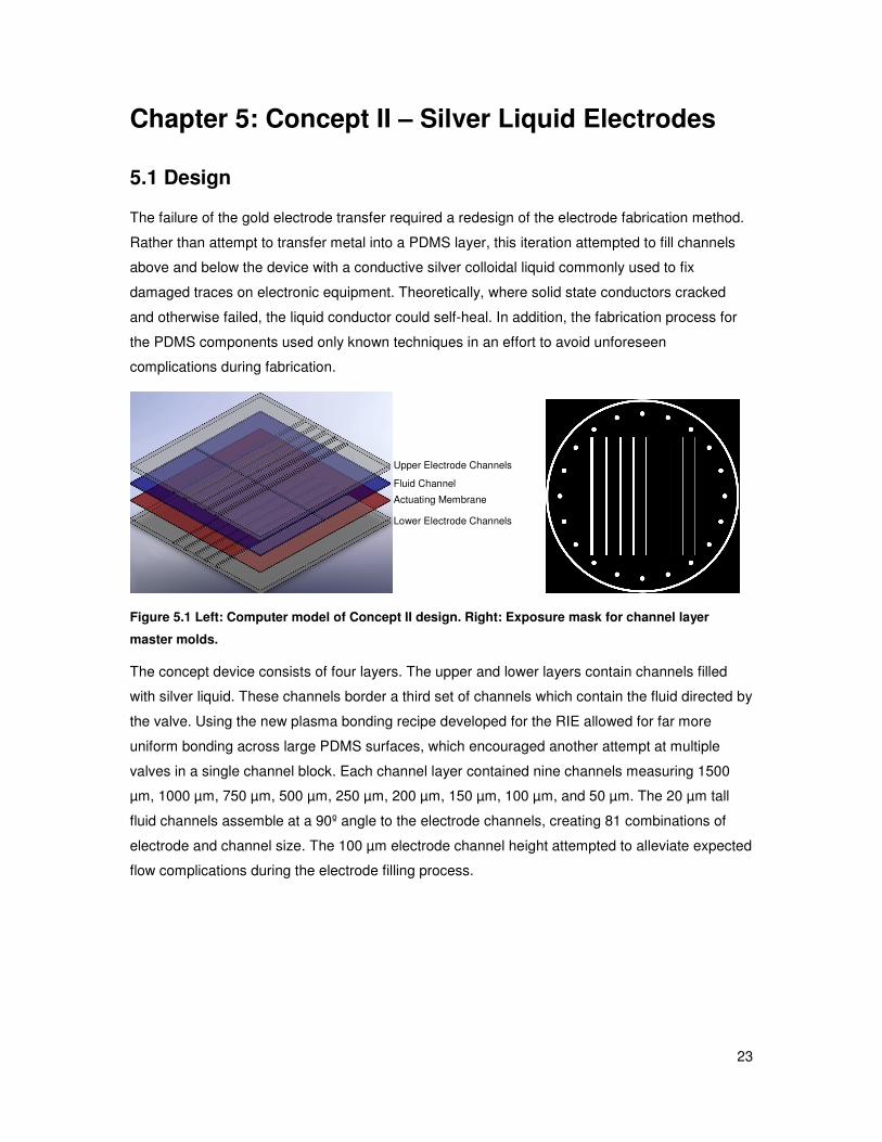
Chapter 5: Concept II – Silver Liquid Electrodes
5.1 Design
The failure of the gold electrode transfer required a redesign of the electrode fabrication method.
Rather than attempt to transfer metal into a PDMS layer, this iteration attempted to fill channels
above and below the device with a conductive silver colloidal liquid commonly used to fix
damaged traces on electronic equipment. Theoretically, where solid state conductors cracked
and otherwise failed, the liquid conductor could self-heal. In addition, the fabrication process for
the PDMS components used only known techniques in an effort to avoid unforeseen
complications during fabrication.
Figure 5.1 Left: Computer model of Concept II design. Right: Exposure mask for channel layer
master molds.
The concept device consists of four layers. The upper and lower layers contain channels filled
with silver liquid. These channels border a third set of channels which contain the fluid directed by
the valve. Using the new plasma bonding recipe developed for the RIE allowed for far more
uniform bonding across large PDMS surfaces, which encouraged another attempt at multiple
valves in a single channel block. Each channel layer contained nine channels measuring 1500
µm, 1000 µm, 750 µm, 500 µm, 250 µm, 200 µm, 150 µm, 100 µm, and 50 µm. The 20 µm tall
fluid channels assemble at a 90º angle to the electrode channels, creating 81 combinations of
electrode and channel size. The 100 µm electrode channel height attempted to alleviate expected
flow complications during the electrode filling process.
Upper Electrode Channels
Actuating Membrane
Fluid Channel
Lower Electrode Channels
Page 34
24
5.2 Fabrication Procedure
Upper and Lower Electrode Channels
1. Pour 30 ml uncured PDMS into petri dish containing electrode channel master mold
2. Degas PDMS in vacuum chamber
3. Cure PDMS in oven at 75 ºC for 45 minutes
4. Cut channel block free from master mold
Actuating membrane
1. Spin coat PDMS onto bare wafer at 2,000 RPM for 30 seconds
2. Cure PDMS in oven at 75 ºC for 45 minutes
Fluid Channel Layer
1. Spin coat PDMS onto bare wafer at 2,000 RPM for 30 seconds
2. Cure PDMS in oven at 75 ºC for 45 minutes
Device Assembly
1. Punch input/output ports into the upper and lower electrode channels.
2. Plasma bond lower electrode channel and fluid channel layer
3. Punch input/output ports into fluid channel layer
4. Plasma bond fluid channel layer and actuating membrane
5. Align and plasma bond actuating membrane and upper channel layer
6. Fill electrode channels with silver colloid
5.3 Fabrication Complications and Solutions
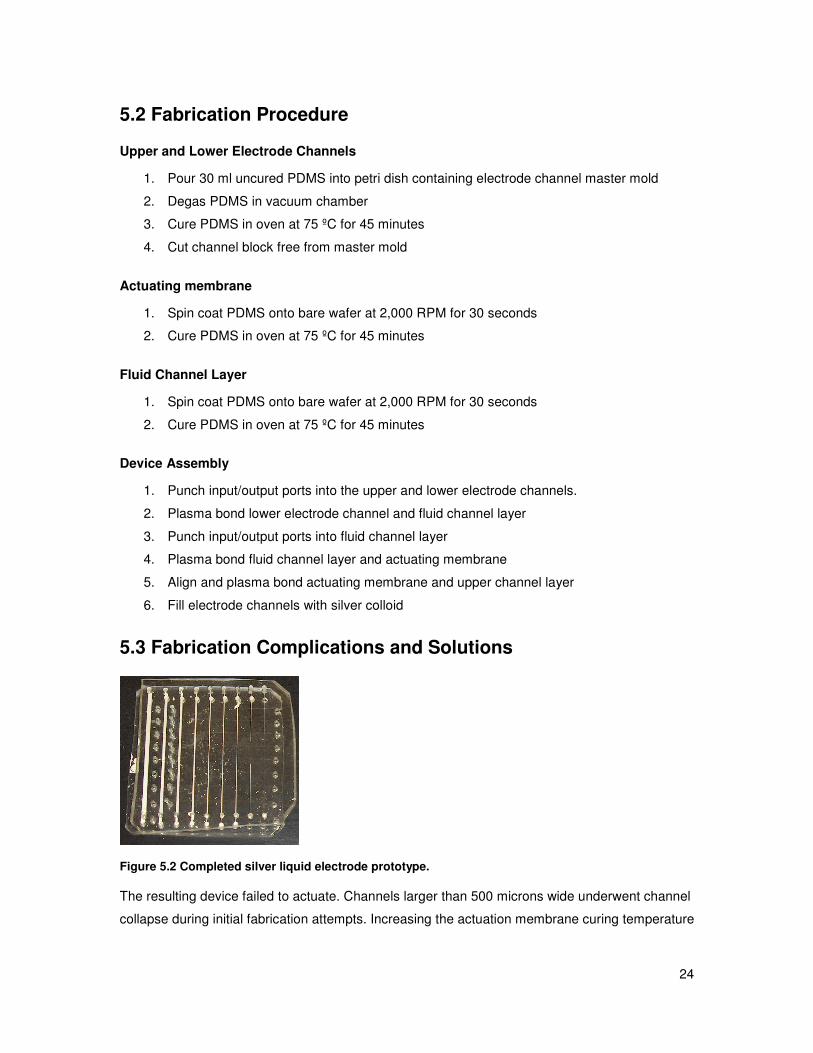
Figure 5.2 Completed silver liquid electrode prototype.
The resulting device failed to actuate. Channels larger than 500 microns wide underwent channel
collapse during initial fabrication attempts. Increasing the actuation membrane curing temperature
Page 35
25
to 135 ºC introduced a small pre-stress into the film and prevented channel collapse in channels
1,000 µm or smaller during later fabrication attempts.
The thinnest channels proved impossible fill with silver liquid, as the pressure would rupture the
membrane at the input port before fully filling the channel. This revealed the primary design flaw
in the chip: the vertical stacking of the input ports left a 40 µm thin film to support the pressures
required to fill the channel. The high pressures required to fill the electrode channels tended to
rupture the membranes sealing the valves and the input ports, leading to extreme cases of
leaking within the chip.
Interfacing with the chip proved impossible due to an unforeseen interaction of the silver liquid
with the PDMS channels. Ideally, the PDMS channels should have prevented the liquid drying
inside the channel itself. However, the permeability of PDMS to air and solvent allowed the silver
colloid to dry and settle. The polymer solution formed a solid insulative casing around the
conductive element, rather than remaining in a liquid state. While ideal for repairing broken
traces, the insulative layer prevented most attempts at interfacing with the traces. The act of
breaking through the casing to interface electrically typically ruptured a membrane in the device
and caused further leaking.
Page 36
26
Chapter 6: Aluminum on PDMS Sputtering
The failure of the liquid silver electrodes required a new method of electrode fabrication. Previous
attempts to sputter aluminum directly onto PDMS substrates had limited success. Aluminum
sputtering would intermittently leave a black scorched surface at points. In some cases scorching
covered the entire substrate.
RF sputtering processes used on PDMS substrates behave oddly due to the insulative nature of
the material. Unlike a conductive or semiconductive material, the charge imparted by the
incoming metal ions cannot dissipate through the material. When these charges build up at
various points on the surface of the substrate, they deflect incoming metal ions away. This
property could cause the point scorching seen in previous sputtering attempts.
Plasma treatment just prior to sputtering uniformly polarizes the surface. A uniformly polarized
surface presents a more stable electrical profile than uncharged PDMS. In theory, the polar
surface could significantly reduce the generation of point charges and allow for more uniform
metal coatings. Unfortunately, the treated surface relaxes quickly at normal room conditions,
normally within 10-15 minutes. The standard operating procedure indicates that pumping down
the sputtering chamber for less than 30-40 minutes can generate contaminated films with poor
conductive properties.
6.1 Experiment I – Plasma Treated Surfaces
This experiment tested the effect of plasma treatment on the quality of aluminum sputtered traces
on PDMS surfaces.
Experiment I Procedure
1. Use a Kapton tape shadowmask to cover all PDMS areas except a 2 mm wide line.
2. Treat substrate in RIE at 20 W and 308 mT for 15 seconds
3. Place substrate in sputtering chamber and pump down for 45 minutes
4. Sputter aluminum at 8 mT and 60 W for 10 minutes.
5. Remove Kapton mask from substrate.
Page 37
27
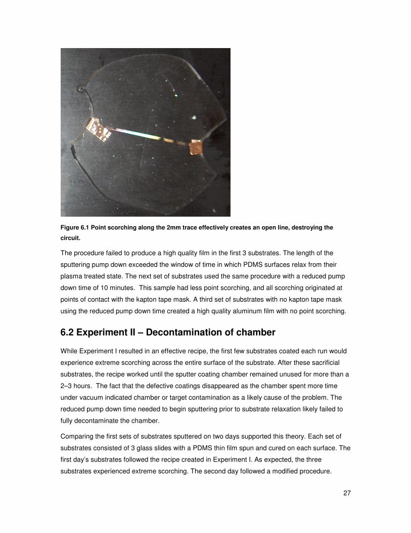
Figure 6.1 Point scorching along the 2mm trace effectively creates an open line, destroying the
circuit.
The procedure failed to produce a high quality film in the first 3 substrates. The length of the
sputtering pump down exceeded the window of time in which PDMS surfaces relax from their
plasma treated state. The next set of substrates used the same procedure with a reduced pump
down time of 10 minutes. This sample had less point scorching, and all scorching originated at
points of contact with the kapton tape mask. A third set of substrates with no kapton tape mask
using the reduced pump down time created a high quality aluminum film with no point scorching.
6.2 Experiment II – Decontamination of chamber
While Experiment I resulted in an effective recipe, the first few substrates coated each run would
experience extreme scorching across the entire surface of the substrate. After these sacrificial
substrates, the recipe worked until the sputter coating chamber remained unused for more than a
2–3 hours. The fact that the defective coatings disappeared as the chamber spent more time
under vacuum indicated chamber or target contamination as a likely cause of the problem. The
reduced pump down time needed to begin sputtering prior to substrate relaxation likely failed to
fully decontaminate the chamber.
Comparing the first sets of substrates sputtered on two days supported this theory. Each set of
substrates consisted of 3 glass slides with a PDMS thin film spun and cured on each surface. The
first day’s substrates followed the recipe created in Experiment I. As expected, the three
substrates experienced extreme scorching. The second day followed a modified procedure.
Page 38
28
Experiment II Procedure
1. Pump down sputtering chamber for 1 hour.
2. Sputter aluminum onto empty chamber for 5 minutes.
3. Use a Kapton tape shadowmask to cover all PDMS areas except a 2 mm wide line.
4. Treat substrate in RIE at 20 W and 308 mT for 15 seconds
5. Place substrate in sputtering chamber and pump down for 45 minutes
6. Sputter aluminum at 8 mT and 60 W for 10 minutes.
7. Remove Kapton mask from substrate.
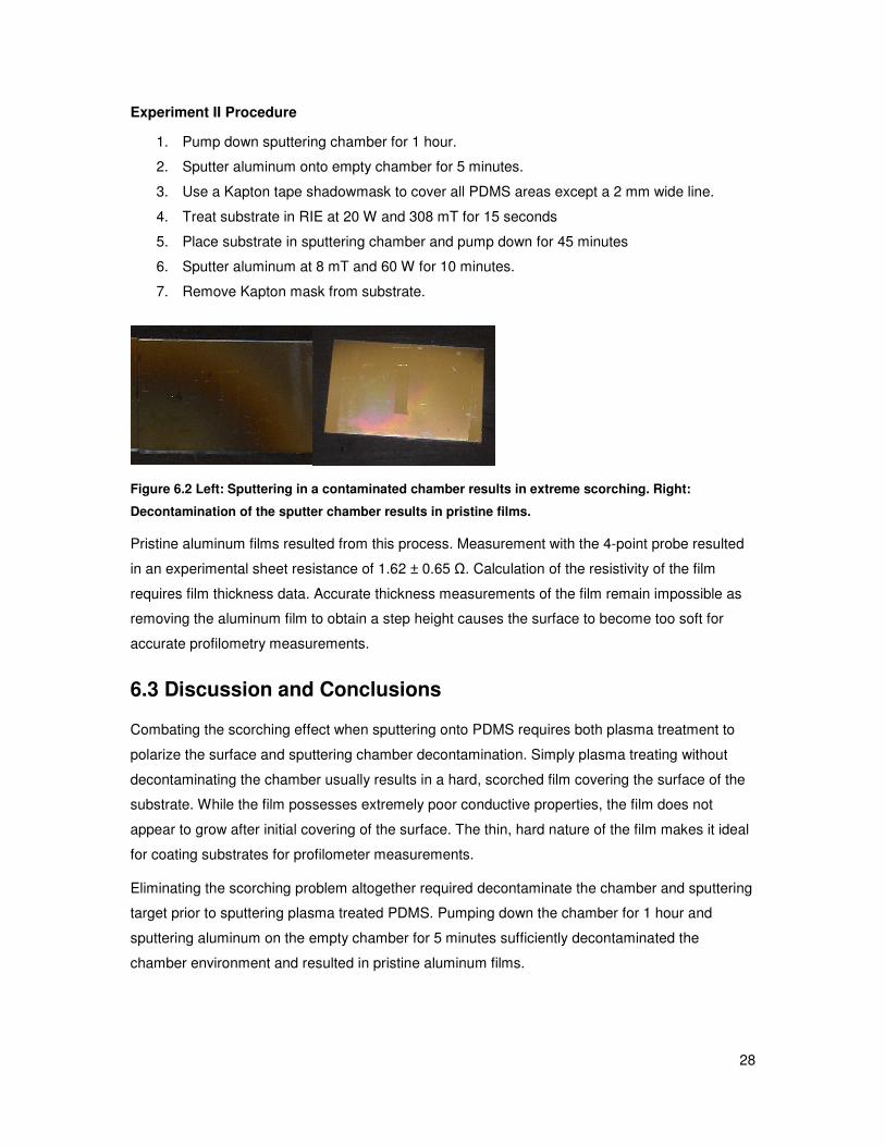
Figure 6.2 Left: Sputtering in a contaminated chamber results in extreme scorching. Right:
Decontamination of the sputter chamber results in pristine films.
Pristine aluminum films resulted from this process. Measurement with the 4-point probe resulted
in an experimental sheet resistance of 1.62 ± 0.65 Ω. Calculation of the resistivity of the film
requires film thickness data. Accurate thickness measurements of the film remain impossible as
removing the aluminum film to obtain a step height causes the surface to become too soft for
accurate profilometry measurements.
6.3 Discussion and Conclusions
Combating the scorching effect when sputtering onto PDMS requires both plasma treatment to
polarize the surface and sputtering chamber decontamination. Simply plasma treating without
decontaminating the chamber usually results in a hard, scorched film covering the surface of the
substrate. While the film possesses extremely poor conductive properties, the film does not
appear to grow after initial covering of the surface. The thin, hard nature of the film makes it ideal
for coating substrates for profilometer measurements.
Eliminating the scorching problem altogether required decontaminate the chamber and sputtering
target prior to sputtering plasma treated PDMS. Pumping down the chamber for 1 hour and
sputtering aluminum on the empty chamber for 5 minutes sufficiently decontaminated the
chamber environment and resulted in pristine aluminum films.
Page 39
29
Chapter 7: Concept III – Aluminum Electrodes
7.1 Iteration I – Flexible backbone
The ability to sputter aluminum directly onto PDMS allowed new electrode fabrication techniques.
Concept III used aluminum electrodes to deliver an actuation voltage to the valve. The design
began as a revision of the original gold electrode concept, modified slightly to account for
differences in process techniques.
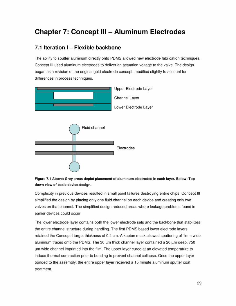
Figure 7.1 Above: Grey areas depict placement of aluminum electrodes in each layer. Below: Top
down view of basic device design.
Complexity in previous devices resulted in small point failures destroying entire chips. Concept III
simplified the design by placing only one fluid channel on each device and creating only two
valves on that channel. The simplified design reduced areas where leakage problems found in
earlier devices could occur.
The lower electrode layer contains both the lower electrode sets and the backbone that stabilizes
the entire channel structure during handling. The first PDMS based lower electrode layers
retained the Concept I target thickness of 0.4 cm. A kapton mask allowed sputtering of 1mm wide
aluminum traces onto the PDMS. The 30 µm thick channel layer contained a 20 µm deep, 750
µm wide channel imprinted into the film. The upper layer cured at an elevated temperature to
induce thermal contraction prior to bonding to prevent channel collapse. Once the upper layer
bonded to the assembly, the entire upper layer received a 15 minute aluminum sputter coat
treatment.
Upper Electrode Layer
Channel Layer
Lower Electrode Layer
Electrodes
Fluid channel
Page 40
30
7.2 Iteration I Fabrication
Lower Electrode Layer
1. Pour 0.4 cm thick block of PDMS
2. Pump down sputtering chamber for 1 hour
3. Cure in oven for 45 minutes at 75 ºC
4. Apply Kapton tape shadowmask
5. Plasma treat masked PDMS block at 308 mT and 20 W for 15 seconds
6. Immediately transfer PDMS to sputtering and pump down for 8 minutes
7. Pre-sputter aluminum for 1 minute at 60 W and 9 mT
8. Open sputter shield and sputter aluminum for 15 minutes at 60 W and 9 mT
9. Remove block from sputter chamber and remove Kapton shadowmask
Channel Layer
1. Spin 30 µm thin film of PDMS over 20 µm tall SU-8 master channel mold
2. Cure in oven for 45 minutes at 75 ºC
Upper Electrode Layer
1. Spin 20 µm thin film of PDMS over silicon wafer treated with JerseyCote
2. Cure in oven for 20 minutes at 135 ºC
Assembly
1. Plasma treat Lower Electrode Layer and Channel Layer for 15 sec at 308 mT and 20 W
2. Place treated surfaces in contact and cure in oven at 75 ºC
3. Plasma treat Channel Layer and Upper Electrode Layer for 15 sec at 308 mT and 20 W
4. Place treated surfaces in contact and cure in oven at 75 ºC
5. Plasma treat Upper Electrode Layer for 15 seconds at 308 mT and 20 W
6. Immediately transfer device to sputtering chamber
7. Pump down chamber for 8 minutes
8. Pre-sputter aluminum for 1 minute at 60 W and 9 mT
9. Open sputter shield and sputter aluminum for 15 minutes at 60 W and 9 mT
10. Remove device from chamber
11. Isolate and attach copper conductive tape to lower traces and upper ground layer
Page 41
31
7.3 Fabrication Complications
The Lower Electrode Layer could not supply adequate support during handling to function as a
backbone. Severe cracking of the aluminum films occurred during handling. The lower electrodes
rarely survived plasma bonding of the channel layer without extreme cracking problems. The
Kapton tape method of electrode patterning also resulted in mild point scorching even after
plasma treatment and decontamination.
The lack of easy access to the lower electrodes resulted in damage during electrical packaging
procedures. The upper PDMS layers of the electrostatic valve blocked electrical contact to the
lower electrodes. The act of removing the upper layers covering the electrode contacts typically
destroyed the trace itself in the process.
Accessing these electrodes required selective removal of the PDMS layers above the electrodes
without high mechanical strain or excessive scraping of the substrate below. Selectively bonding
the upper layers allowed selective removal of specific sections of PDMS away from the active
area of the device.
Generating a selective bond required a small modification of the plasma treatment process. A
Kapton tape shadowmask applied to the surface prior to placing the substrates into the plasma
treatment chamber prevented treatment of the masked areas. The untreated areas did not bond
during the oven curing step and created a removable flap. This flap protected the interface area
of the lower traces during processing, prior to removal during the packaging stage of assembly.
7.4 Iteration II – Glass Backbone
Switching to 2 in x 3 in glass substrates for the Lower Electrode Layer allowed access to known
lithography and wet etching methods, and provided the necessary support to prevent severe
cracking of the lower aluminum electrode. Changing the backbone substrate to glass slides
required significant alteration of the fabrication process of PDMS layers.
Any SU-8 structures built onto a silicon master mold typically create minor irregularities in the
surface of any PDMS thin films spun onto the mold. Unlike a PDMS block, a glass substrate does
not compress during the contact phase of bonding. Irregularities in the surface of a PDMS layer
can generate air pockets when attempting to bond to a bare glass substrate and cause
widespread bond failure.
Additionally, release layers used in prior fabrication methods proved ineffective. Once a glass
substrate bonded to a thin film coated onto a silicon wafer, the rigidity and brittleness of the
substrates prevented the peeling action required to release the PDMS layer. Attempting to
separate the PDMS layer invariably resulted in the shattering of either the glass slide or the SU-8
Page 42
32
master mold. The glass slide backbone required more flexible mold substrates. Plastic petri
dishes used as spincoating platforms by other projects allowed a semistable platform for
spincoating with a degree of flexibility, allowing the necessary peeling action during release.
Plastic mold substrates present a key design problem. Wet chemistries used to develop SU-8
photoresist severely damage plastic substrates. This forces the use of other molding methods
and leads to problems creating channel layers with proper tolerances.
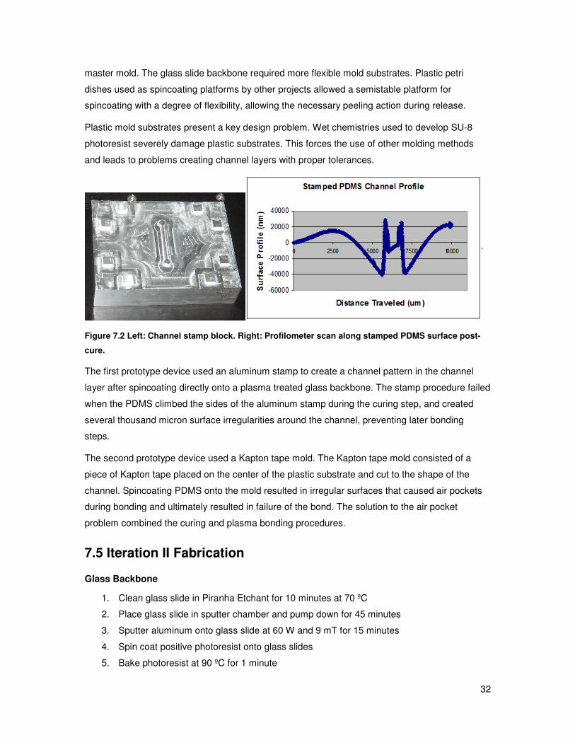
Figure 7.2 Left: Channel stamp block. Right: Profilometer scan along stamped PDMS surface post-
cure.
The first prototype device used an aluminum stamp to create a channel pattern in the channel
layer after spincoating directly onto a plasma treated glass backbone. The stamp procedure failed
when the PDMS climbed the sides of the aluminum stamp during the curing step, and created
several thousand micron surface irregularities around the channel, preventing later bonding
steps.
The second prototype device used a Kapton tape mold. The Kapton tape mold consisted of a
piece of Kapton tape placed on the center of the plastic substrate and cut to the shape of the
channel. Spincoating PDMS onto the mold resulted in irregular surfaces that caused air pockets
during bonding and ultimately resulted in failure of the bond. The solution to the air pocket
problem combined the curing and plasma bonding procedures.
7.5 Iteration II Fabrication
Glass Backbone
1. Clean glass slide in Piranha Etchant for 10 minutes at 70 ºC
2. Place glass slide in sputter chamber and pump down for 45 minutes
3. Sputter aluminum onto glass slide at 60 W and 9 mT for 15 minutes
4. Spin coat positive photoresist onto glass slides
5. Bake photoresist at 90 ºC for 1 minute
Page 43
33
6. Expose photoresist using aluminum trace mask for 16 seconds
7. Develop photoresist in CD-26 for 10 minutes
8. Etch Aluminum using Transene Type A etchant
9. Strip photoresist using acetone
10. Etch any aluminum on sides of glass slide using Transene Type A etchant
Channel Layer
1. Apply Kapton tape to plastic substrate
2. Cut Kapton tape to shape of channel structure
3. Pour liquid PDMS onto center of petri dish
4. Apply Kapton tape selective bonding mask to glass backbone
5. Plasma treat glass backbone in RIE at 308 mT and 20 W for 30 seconds
6. Remove Kapton tape selective bonding mask
7. Press treated glass backbone into liquid PDMS
8. Place plastic substrate onto aluminum block in oven and place aluminum weight onto
glass backbone
9. Cure in oven at 75 ºC for 45 minutes
10. Peel plastic substrate away from glass backbone and channel layer.
Actuating Membrane
1. Spin coat PDMS onto plastic substrate at 2000 RPM for 30 seconds
2. Cure in oven at 135 ºC for 15 minutes
Assembly
1. Plasma treat channel layer and actuating membrane in RIE at 308 mT and 20 W for 15
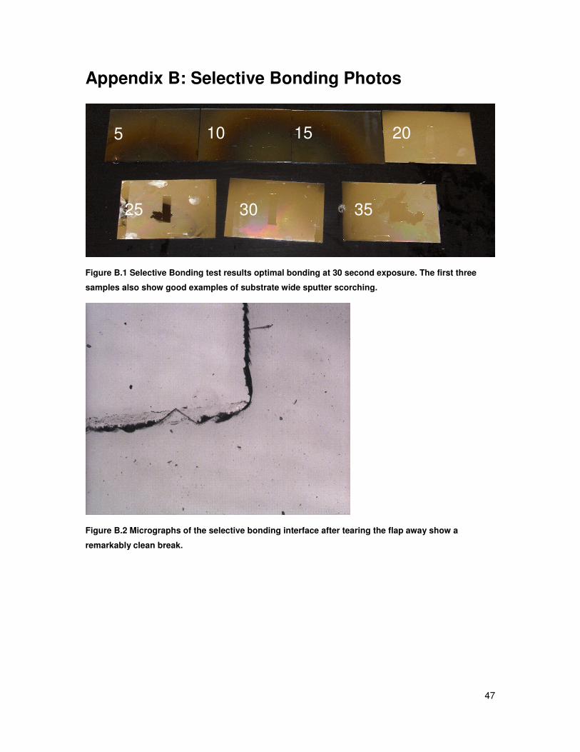
seconds
2. Place channel layer and actuating membrane in contact and cure in oven at 75 ºC for 30
minutes
3. Pump down sputtering chamber for 1 hour
4. Peel valve assembly from plastic substrate
5. Plasma treat valve assembly in RIE at 308 mT and 20 W for 15 seconds
6. Transfer valve assembly to sputtering chamber
7. Pump down chamber for 8 minutes
8. Pre-sputter aluminum for 1 minute at 60 W and 9 mT
9. Open sputter shield and sputter aluminum for 15 minutes at 60 W and 9 mT
10. Remove device from chamber
11. Remove selectively bonded flaps to expose lower traces
12. Isolate and attach copper conductive tape to lower traces and upper ground layer
Page 44
34
7.6 Fabrication Complications
Iteration II marked the first successful fabrication of a testable prototype. All electrodes tested
positive for connection macroscopically and no fluid leaks occurred. One of the valves collapsed
during bonding, leaving one valve intact. This valve did not actuate upon application of a driving
voltage.
Figure 7.3 Left: Top of Prototype Electrostatic Valve. Right: Underside of prototype electrostatic
Valve.
Investigating the valve failure revealed two possible causes. Localized cracking at the channel
edges prevented a driving voltage from applying across the channel properly. The cracking
formed bands of isolated aluminum over the valve itself. These isolated bands received no driving
voltage and effectively cut the upper electrode from the circuit entirely.
Additionally, a cross section of two channel layers from devices that never completed fabrication
revealed extreme inconsistency in the distance between the bottom of the channel layer and the
lower electrodes. Without precise control of the distance between the electrodes the driving
voltage became extremely difficult to predict.
7.7 Conclusions
Aluminum sputtering can successfully create a conductive layer on PDMS. However, the fragility
of the sputtered layers causes major fabrication complications. Attempts to stabilize the aluminum
with rigid substrates met with moderate success. Aluminum layers on PDMS with direct rigid
substrate support eliminate widespread cracking problems but retain localized cracking problems
near surface irregularities.
Patterning of aluminum on PDMS presents severe difficulties. Shadowmasking PDMS layers
engendered scorching during the sputtering steps, and wet etching processes performed on
PDMS supported aluminum led to damage to the PDMS layer under the aluminum. Generating a
patterned aluminum trace on PDMS layers proved impossible to achieve. Layer-wide sputtering
Page 45
35
of aluminum showed promise as effective ground layers in areas away from device geometry.
The severe cracking which occurs near device geometries on layers below the aluminum layer
made aluminum a non-ideal material for electrode fabrication.
Page 46
36
Chapter 8: Aluminum Cracking Investigation
The capacitive circuit used in the valve required no actual flow of electrons across the valve itself.
The charge sourced on one side of a crack should have induced a voltage bias and transferred at
least some voltage to the valve itself, yet applying a voltage across the valve generated no
detectable movement of the concept III valve. Assessing the viability of aluminum electrodes
required explaining why the capacitive nature of the circuit did not overcome the cracking
problem.
Four major handling conditions can cause cracking. Light contact with the surface from fingers or
other objects causes slight localized cracking. Removal of Kapton masks used to pattern
aluminum on PDMS creates regions of cracking around the interfaces during lift off. The act of
lifting off a PDMS layer supporting an aluminum film creates extreme cracking. Finally, any
bending of the substrate creates significant cracking across the entire aluminum film.
8.1 Light Contact
Micrographs of light contact on an aluminum on PDMS film revealed cracking in radial patterns
emanating from the point of contact.
Figure 8.1 Light contact cracking creates a radial pattern of closed aluminum cells.
Page 47
37
Most notably, the patterns created small cells of aluminum isolated by cracks on all sides. These
cracks emanate from the central point of pressure from any given light contact. The pressure
applied by light contact deforms the thin film of PDMS supporting the aluminum film locally. The
PDMS elongates at a rate the aluminum cannot match and cracking occurs quickly due to the
fragility of aluminum films only hundreds of nanometers thick.
8.2 Kapton Removal
Removing Kapton tape from aluminum sputtered onto a PDMS surface left extreme surface
cracking in any film under the tape as well as fringe effects at the edge of the tape-substrate
interface.
Figure 8.2 Removing Kapton tape from an aluminum film causes extreme surface damage and
formation of isolated cells.
When the Kapton tape peels from the surface, the PDMS film deforms under the stress well
beyond the ductility of the brittle aluminum film. The area near the tape also deforms to a lesser
degree, generating the fringe cracking. Eliminating the scorching problem caused by Kapton tape
masking remains pointless because this edge cracking alone will isolate large sections of any
aluminum trace patterned with Kapton masking.
Page 48
38
8.3 Lift Off and Peeling
Removing an aluminum coated PDMS layer from a glass substrate effectively replicated the
mechanical stress imposed on the aluminum film during a standard lift off via peeling procedure.
Figure 8.3 Peeling of aluminum coated thin films creates isolated rectangular cells.
Micrographs of the peeling interface show rectangular cracking patterns. This rectangular pattern
appears to only appear under lift off conditions, as tension occurs in multiple directions at the
same time. These rectangular cracks create obvious electrical isolation between cells.
8.4 Substrate Bending
Bending any substrate with an aluminum film creates fairly large damage to the film itself.
Examining samples from the first iteration of concept III reveals heavy cracking from bending
during handling.
Page 49
39
Figure 8.4 Aluminum traces on PDMS blocks show extreme cracking after even minor amounts of
handling.
While the kapton tape used to mask these samples causes most of the cracking at the sides of
the traces, the central cracking only appears after a few hours of handling. PDMS substrates
prove far too flexible to support aluminum traces without additional structural support in the form
of a glass backbone.
8.5 Conclusions
The degree of cracking occurring under normal handling procedures creates isolated cells in the
aluminum traces. These cells demonstrated an interesting difference between the theoretical
diagram for the valve circuit and reality. In the original circuit theory, induced voltage across
cracks should have generated enough charge at the active portion of the circuit to actuate the
device. This theory hinged on relatively minor cracking. The sheer amount of cracking created a
device with not just one or two cracks to induce a voltage across, but thousands. Even if the
source voltage induced a voltage in all of these cells, predicting the relative voltage to the ground
electrode remains impossible. Additionally, while sections of each cell became charged, that
charge never resulted in a net increase or decrease in electrons present in the bulk electrode.
The force generated by the charge never increased enough to actuate the valve.
Page 50
40
The presence of these isolated cells within the active area of a valve removed any chance of the
valve functioning. The brittleness of aluminum films revealed during handling makes aluminum
non-viable as an electrode material. A viable electrostatic valve required another material switch.
Page 51
41
Chapter 9: Findings and Future Work
9.1 Summary of Findings
Fabrication of an electrostatic switch ultimately remained unsuccessful. The additional materials
and development time required to take the next logical step after the failure of concept III
exceeded the remaining resources and allotted timeframe of this master’s thesis. While the
concept designs failed to result in a working device, each concept has added significantly to the
knowledge base of the Cal Poly Clean Room.
Concept I attempted to reproduce the results of a paper describing the process to transfer gold
films into PDMS. Exact replication of the conditions of the experiment required unavailable
equipment, and all attempts to modify the process to fit clean room technology failed. Moving to
oxide release films showed that reducing adhesion prior to patterning caused failure of the
metallic film during wet etching.
Plasma bonding experiments allowed the creation of recipes for bonding of PDMS blocks to both
glass and other PDMS blocks. PDMS to glass bonding requires 30 seconds of exposure to O2
plasma at 308 mT and 20 W, while PDMS to PDMS bonding requires 15 seconds of exposure to
O2 plasma at 308 mT and 20 W.
Concept II complications led to a thermal pre-stress technique used to prevent channel collapse
during fabrication steps. Increasing the cure temperature of the thin membrane covering a
channel to 135 ºC induces enough pre-stress to prevent channel collapse in channels up to 1,000
µm wide.
Concept II showed improper placement of interface points in multilayer devices can lead to
severe leaking. Active device areas require structures with a sufficient bonding area to separate
active device areas or device pressures can cause bonds or layer integrity to fail.
Concept II also showed the air and solvent permeability of PDMS can allow solvent based
suspensions to dry within channels.
Aluminum sputtering experiments showed plasma exposure of PDMS helped eliminate the effect
of point charges during sputtering, which eventually led to a process to sputter both pristine
aluminum films and hard glassy coatings. The aluminum coatings proved extremely useful for
taking profilometer readings of PDMS step heights.
Concept III, Iteration I showed the need for access flaps to reach lower electrode interfaces.
Shadow masking during plasma treatment allowed the creation of partial bonds that in turn
allowed easy removal of trace coverings.
Page 52
42
Iteration I also showed PDMS backbones failed to protect against cracking in the metallic thin
film. Iteration II used glass backbone layers help eliminate most cracking of aluminum films
sputtered onto PDMS. However, critical areas near device features still exhibited severe cracking.
Fabricating valves directly onto a glass backbone created greater fabrication complications than
the change resolved.
Stamping fabrication techniques showed that small surface irregularities can prevent full contact
of two treated surfaces during plasma bonding. Lack of contact between surfaces prevents
bonding in those areas and invariably leads to leaking and failure.
The aluminum cracking investigation showed cracking of aluminum films resulted in small,
isolated cells which prevented net charge buildup over the active valve area. PDMS layers simply
cannot provide the mechanical support necessary to eliminate cellular cracking of brittle metallic
films in device critical areas.
9.2 Recommendations for Future Work
The results of concepts I, II, and III lead to the following guidelines for future PDMS-based
electrostatic work at Cal Poly.
1. Use as few layers as possible. Each layer added to a device compounds the chances of
failure exponentially, as all previous points of failure can fail during bonding as well as all
new critical areas on the added layer.
2. Reduce layer complexity to a minimum. Leave at least 10,000 µm between fluid channels
whenever possible to avoid leaking.
3. Avoid using brittle materials in PDMS based devices. The lack of rigid support from
PDMS during fabrication and handling processes render brittle materials non-ideal for
PDMS based microfluidic devices.
4. Use large valve structures. Valves less than 500 µm wide quickly increase the amount of
voltage required to close the valve exponentially.
Options for further research into valve electrodes include Dow Corning® DA 6254 and electrically
conductive polymers. DA 6254 contains over 60% silver particles suspended in PDMS with
adhesive components. Adding high amounts of silver to Sylgard 184 could create similar
compounds without the adhesive properties. Electrically conductive polymers also represent a
possible avenue of research into flexible, micropatternable, electrodes.
Metallization with more ductile metals such as copper could also solve the cracking problems.
Electronics applications have used copper coated polymers as flexible connectors for many
years.
Page 53
43
Further research into thermal pre-stressing of PDMS membranes could greatly increase the
maximum channel width available to PDMS devices created in the Cal Poly Clean Room.
Selective bonding presents an opportunity for a highly valuable research project. Selective
bonding techniques could provide further expansion of the tools available in soft lithography
processes and further open multilayer design possibilities.
Aluminum sputtered PDMS layers allow creation of proper PDMS spin speed curves. These
curves could remove a significant amount of trial and error from the fabrication process and
heavily increase device yield in all PDMS based microfluidics at Cal Poly.
Page 54
44
References
[1] S. K. Sia and G. M. Whitesides. Microfluidic Devices Fabricated in Poly(dimethylsiloxane) for
Biological Studies. Electrophoresis. 2003. 24: 3563-3576.
[2] J. M. K. Ng, I. Gitlin, A. D. Stroock, and G. M. Whitesides. Components for Integrated
Poly(dimethylsiloxane) Microfluidic Systems. Electrophoresis. 2002. 23: 3461-3473.
[3] Z. Yang, S. Matsumoto, H. Goto, M. Matsumoto, and R. Maeda. Ultrasonic Micromixer for
Microfluidic Systems. Sensors and Actuators A. 2001. 93. 266-272.
[4] T. N. T. Nguyen, M-C. Kim, J-S. Park, and N-E. Lee. An Effective Passive Microfluidic Mixer
Utilizing Chaotic Advection. Sensors and Actuators B. 2008.
[5] V. Studer, G. Hang, A. Pandolfi, M. Ortiz, W. F. Anderson and S. R. Quake. Scaling Properties
of a Low-Actuation Pressure Microfluidic Valve. Journal of Applied Physics. 2004. 95: 393-398.
[6] M. Yamada and M. Seki. Nanoliter-Sized Liquid Dispenser Array for Multiple Biochemical
Analysis in Microfluidic Devices. Anal. Chem. 2004. 76: 895-899.
[7] O. C. Jeong, and S. Konishi. Fabrication and Drive Test Pneumatic PDMS Micro Pump.
Sensors and Actuators A. 2007. 135: 849-856.
[8] W. H. Grover, A. M. Skelly, C. N. Liu, E.T. Lagally and R. A. Mathies. Monolithic Membrane
Valves and Diaphragm Pumps for Practical Large-Scale Integration into Glass Microfluidic
Devices. Sensors and Actuators B. 2003. 89: 315-323.
[9] J. Wang. Portable Electrochemical Systems. Trends in Analytical Chemistry. 2002. 21:226-
232,
[10] J. C. McDonald and G. M. Whitesides. Poly(dimethylsiloxane) as a Material for Fabricating
Microfluidic Devices. Accounts of Chemical Research. 2002. 35: 491-499.
[11] S. R. Quake and A. Scherer. From Micro- to Nanofabrication with Soft Materials. Science.
2000. 290: 1536-1539.
[12]. Thuillier and C. K. Malek. Development of a Low Cost Hybrid Si/PDMS Multi-layered
Pneumatic Microvalve. Microsyst. Technol. 2005. 12: 180-185.
[13] See www.coleparmer.com
[14] M. A. Unger, H-P. Chou, T. Thorsen, A. Scherer, and S. R. Quake. Monolithic
Microfabricated Valves and Pumps by Multilayer Soft Lithography. Science. 2000. 288: 113-116.
[15] See www.dowcorning.com
Page 55
45
[16] J.C. Lötters, W. Olthuis, P. H. Veltink, and P. Bergveld. The Mechanical Properties of the
Rubber Elastic Polymer Polydimethylsiloxane for Sensor Applications. J. Micromech. Microeng.
1997. 7:145-147.
[17] H. Yang, Q. T. Nguyen, Y. Ding, Y. Long, and Z. Ping. Investigation of poly(dimethyl
siloxane) (PDMS)-solvent interactions by DSC. Journal of Membrane Science. 2000. 164: 37-43
[18] see www.filmetrics.com
[19] S. Middlemann and A. Hochberg. Process Engineering Analysis in Semiconductor Device
Fabrication. McGraw-Hill College. 1993. 313-320
[20] See www.microchem.com
[21] C. Liu. Foundations of MEMS. Pearson Education. 2006.
[22] E. P. Kartalov, A. Scherer, S. R. Quake, C. R. Taylor and W. F. Anderson. Experimentally
Validated Quantitative Linear Model for the Device Physics of Elastomeric Microfluidic Valves.
Journal of Applied Physics. 2007. 101
[23] K. J. Lee, K. A. Fosser, and R. G. Nuzzo. Fabrication of Stable Metallic Patterns Embedded
in Poly(dimethylsiloxane) and Model Applications in Non-Planar Electronic and Lab-on-a-Chip
Device Patterning. Advanced Functional Materials. 2005. 15: 557-566.
Page 56
46
Appendix A: PDMS Thin Film Data
Figure A.1 Step height of 1500 RPM and 2000 RPM Thin Films after metallization and cross
sectioning.
Page 57
47
Appendix B: Selective Bonding Photos
Figure B.1 Selective Bonding test results optimal bonding at 30 second exposure. The first three
samples also show good examples of substrate wide sputter scorching.
Figure B.2 Micrographs of the selective bonding interface after tearing the flap away show a
remarkably clean break.
5 10 15 20
25 30 35