Page 1
1
Design, fabrication and low-power RF measurement
of an X-band dielectric-loaded accelerating
structure
Yelong Wei, 1, 6* Hikmet Bursali 1, 2, Alexej Grudiev 1, Ben Freemire 3, Chunguang Jing 3,4,
Joel Sauza Bedolla 5, Rolf Wegner 1, and Carsten Welsch6
1CERN, Geneva CH-1211, Switzerland
2Sapienza University of Rome, Rome, Italy
3Euclid Techlabs LLC, Bolingbrook, Illinois 60440, USA
4High Energy Physics Division, Argonne National Laboratory, Lemont, Illinois 60439, USA
5Lancaster University, Lancaster, UK
6University of Liverpool and Cockcroft Institute, UK
Abstract: Dielectric-loaded accelerating (DLA) structures are being studied as an alternative to
conventional disk-loaded copper structures to produce the high accelerating gradient. This
paper presents the design, fabrication and low-power RF measurement of an externally-
powered X-band DLA structure with a dielectric constant 휀r = 16.66 and a loss tangent
tan𝛿 = 3.43 × 10⁻⁵. A dielectric matching section for coupling the RF power from a circular
waveguide to an X-band DLA structure consists of a very compact dielectric disk with a width
of 2.035 mm and a tilt angle of 60°, resulting in a broadband coupling at a low RF field which
has the potential to survive in the high-power environment. Based on simulation studies, a
prototype of the DLA structure was fabricated. Results from bench measurements and their
comparison with design values are presented. The detailed analysis on the fabrication error
which may cause the discrepancy between the RF measurements and simulations is also
discussed.
I. Introduction
Over the past few decades, there has been a major
effort to understand the high gradient limits of
conventional disk-loaded metal accelerating
structures, as well as to develop alternative
structures that may be capable of producing high
gradient. One promising concept is the dielectric-
loaded accelerating (DLA) structures which utilize
dielectrics to slow down the phase velocity of
travelling waves in the vacuum channel. A DLA
structure comprises a simple geometry where a
dielectric tube is surrounded by a conducting
cylinder. The simplicity of DLA structures offers
great advantages for fabrication of high frequency
(>10 GHz) accelerating structures, as compared with
conventional metallic accelerating structures which
demand extremely tight fabrication tolerances. This
is of great importance in the case of linear colliders,
where tens of thousands of accelerating structures
have to be built. Moreover, the relatively small
diameter of DLA structures facilitates the use of
quadrupole lenses around the structures. The DLAs
are also advantageous in terms of the ease of
applying damping schemes for beam-induced
deflection modes [1-2], which can cause bunch-to-
bunch beam breakup and intrabunch head-tail
instabilities [3].
The DLA structures were initially proposed in the
1940s [4-7], and experimentally demonstrated in the
1950s [8-10]. Since that time, disk-loaded metallic
structures have prevailed for accelerator research
and development because of their high quality factor
and high field holding capability. Thanks to
remarkable progress in new ceramic materials with
high dielectric permittivity (εr > 20), low loss
*[email protected]
Page 2
2
(tan 𝛿 ≤ 10−4) [11-13], and ultralow-loss (tan 𝛿 ≤
10−5 ) [14-15], studies on DLA structures are
gradually being revived. For example, fused silica,
chemical vapor deposition (CVD) diamond, alumina
and other ceramics have been proposed as materials
for DLA structures [16-18], and experimentally
tested with high-power wakefield accelerating
structures at Argonne National Laboratory [19-22].
In the last two decades, different kinds of DLA
structures with improved performance have been
reported, such as a dual-layered dielectric structure
[23], a hybrid dielectric and iris-loaded accelerating
structure [24], a multilayered dielectric structure
[25], a disk-and-ring tapered accelerating structure
[26], a dielectric disk accelerating structure [27], and
a dielectric assist accelerating structure [28-31].
Since a high accelerating gradient of up to 100
MV/m has been demonstrated at room temperature
for an X-band copper structure [32-33], high-
gradient X-band technology have received
considerable attention from the light-source [34-37]
and medical [38-40] communities. Building on these
developments, a DLA structure operating at a high
frequency (X-band) appears to be very promising for
future linear accelerators.
We describe in this paper a detailed design,
fabrication and low-power RF measurement of an
X-band DLA structure. In order to efficiently couple
the RF power from a rectangular waveguide to an X-
band DLA structure, two modules are adopted (see
Fig. 1): a TE10-TM01 mode converter with choke
geometry and a dielectric matching section. The
mode converter is used to convert the TE10 mode
from a rectangular waveguide to the TM01 mode in
a circular waveguide. The dielectric matching
section provides a good match for the impedance of
the TM01 mode between the circular waveguide and
the DLA structure. A choke flange separates the
DLA structure from the mode converter and thus
makes the mode converter independent of the
dielectric properties. In this case, the mode converter
can be reused for similar experiments operating at
the same frequency. Section II presents detailed RF
design of an X-band DLA structure and dielectric
matching sections with a dielectric constant 휀r =
16.66 and a loss tangent tan𝛿 = 3.43 × 10⁻⁵ .
Section III shows the fabrication process for
obtaining the prototypes of mode converters and
DLA structure. Section IV presents the low-power
RF measurement for the full-assembly prototypes
and its comparison with the simulations. Section V
investigates the fabrication errors to cause the
discrepancy between the measurement and the
simulations. Section VI gives the conclusions.
Figure 1. Conceptual illustration of an externally-
powered DLA structure connected with two matching
sections and two TE10-TM01 mode converters with choke
geometry.
II. Design of an X-band DLA
structure and dielectric matching
sections
In this section, the RF properties of an X-band
DLA structure (see Fig. 2) are studied. A dielectric
matching section to efficiently couple the RF power
from a circular waveguide into the DLA structure is
also described in detail.
A. A DLA Structure
Figure 2. Front view and longitudinal cross section of a
cylindrical DLA structure. 휀r, 𝑅in, 𝑅out, and 𝐿 represent
dielectric constant, inner radius, outer radius, and length
for the DLA structure.
MgTiO3 ceramic, with good thermal conductivity
and ultralow power loss, which has been studied in
[17], is chosen as the dielectric material for our DLA
structure. An accurate measurement of the dielectric
properties has to be performed before using such a
ceramic for our RF design. As shown in Fig. 3, a
TE01δ silver-plated resonator, which is designed for
testing ceramics at an X-band frequency, is used to
Page 3
3
measure the dielectric constant 휀𝑟 and loss tangent
tan𝛿 of sample coupons. Four coupons made from
the same dielectric rods as for the fabrication are
measured. A dielectric constant 휀𝑟 = 16.66 and a
loss tangent tan𝛿 = 3.43 × 10⁻⁵ (having error
bars 0.6% of the nominal value) are obtained for the
RF design of the DLA structure and matching
sections which follows.
Figure 3. Measurement setup of the dielectric properties
of the material sample.
The DLA structure could be potentially used for
the CLIC main linac [41-46]. The inner radius is
chosen to be 𝑅in = 3.0 mm from consideration of
the CLIC beam dynamics requirement [43, 44]. The
outer radius is then calculated to be 𝑅out =
4.6388 mm for an operating frequency of 𝑓0 =
11.994 GHz. The group velocity obtained is 𝑣𝑔 =
0.066𝑐, where 𝑐 is speed of light. A quality factor of
𝑄0 = 2829 and a shunt impedance of
𝑅shunt = 26.5 MΩ m are also derived for such a
DLA structure using HFSS [47]. The length of the
DLA structure is chosen as 𝐿 = 100 mm for the
following simulations and mechanical assembly.
B. A Chamfered Dielectric Matching
Section
Through optimization studies [48], a compact,
low-field, broadband matching section with a tilt
angle of 𝜃 = 60° is obtained. In realistic fabrication,
a sharp dielectric corner easily breaks. In order to
prevent such a break, a 45° chamfer with a length of
0.254 mm is added to this corner, as shown in Fig. 4.
The shape of the outer metal is also changed by
rounding with a fillet radius of 𝑅r = 0.322 mm, in
order to prevent field enhancement near that area.
Figure 4 (a) shows the calculated electric field
distribution for the chamfered dielectric matching
section at an input power of 1 W. Figure 4 (b)
indicates that the electric fields near that area are
much lower than those of the DLA structure. In this
case, this dielectric matching section has the
potential to withstand high-power test.
Figure 4. (a) Electric field distribution for the optimum
matching section with a chamfered dielectric corner. (b)
Electric field magnitude along Line AFC which denotes a
section of lines and arcs connected by the points A, F, and
C, as shown in (a), where the distance of point A is taken
as 0 mm.
Figure 5 shows the calculated 𝑆11 = −54 dB and
𝑆21 = − 0.03 dB for the chamfered dielectric
matching section at the operating frequency of
11.994 GHz. The 𝑆11 = −54 dB indicates that the
reflected RF power is negligibly small. Using 𝑆21 =
−0.03 dB, the coupling coefficient is calculated to
be 99.3%. This means that almost 100% of RF
power is efficiently coupled from the circular
waveguide into the DLA structure by using such a
dielectric matching section. The 𝑆21 also has a broad
3 dB bandwidth of more than 1.0 GHz, which allows
greater tolerance to potential fabrication errors.
(a)
(b)
Page 4
4
Figure 5: Simulated 𝑆11 and 𝑆21 as a function of
frequency for the chamfered dielectric matching
section.
C. A Vacuum Microgap
In our realistic fabrication, the entire dielectric
tube, including the matching section and the DLA
structure, is sintered as a single piece. A thin metallic
layer of 0.0508 mm is first coated onto the surface
of the whole dielectric tube. The coated dielectric
tube is then inserted into the outer copper jacket.
However, there is still a microscale vacuum gap
caused by metallic clamping between the thin
metallic coating and the outer thick copper jacket, as
shown in Fig. 6. It is therefore of particular
importance to study the dependence of the S-
parameters and electric fields on the microgap 𝑑2.
Figure 6. Longitudinal cross section of a circular
waveguide, a realistic dielectric matching section with a
vacuum microgap, and a DLA structure.
Figure 7 shows how varying the vacuum microgap
𝑑2 influences 𝑆11 and 𝑆21 . With a larger vacuum
microgap, 𝑆11 increases while 𝑆21 decreases,
resulting in worse matching. For a vacuum microgap
of 𝑑2 = 0.2 mm, 𝑆11 = −32 dB and 𝑆21 = −0.32
dB are obtained, which is still acceptable for our
design. However, 𝑆11 is increased to -28.5 dB and
𝑆21 remains unchanged, when the vacuum microgap
becomes 0.3 mm.
Figure 7. Simulated 𝑆11 and 𝑆21 as a function of vacuum
microgap 𝑑2.
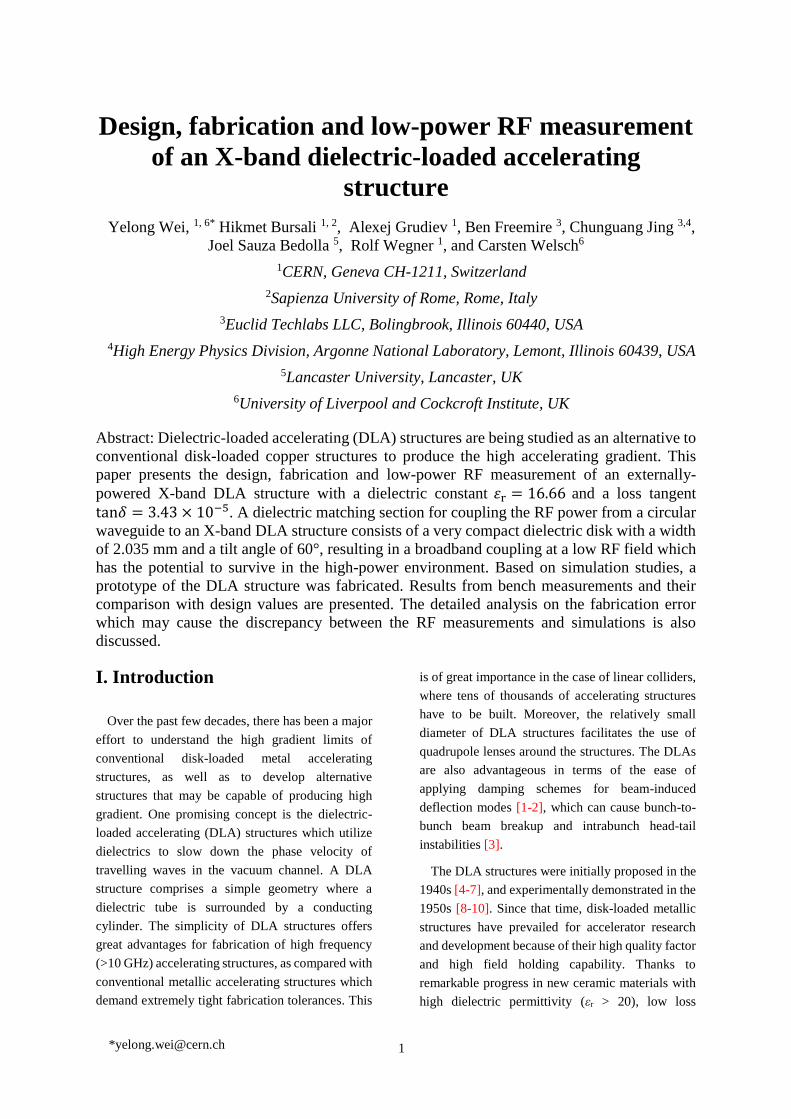
Figure 8 (a) shows the calculated electric field
distribution for the realistic matching section with a
vacuum microgap, at an input power of 1.0 W.
Figure 8 (b) gives the calculated electric field
magnitude along Line AGC for different vacuum
microgaps. There are two peaks in each curve,
indicating the relatively strong fields near the
chamfered corner and rounding corner, respectively.
For a vacuum microgap of 0.3 mm, the peak fields
are higher than those of the DLA structure, which
may cause arcing in a high-power test. The dielectric
matching section is therefore allowed to have a
maximum vacuum microgap of 0.2 mm, in which
RF fields are still lower than those of DLA structure,
𝑆11 is better than -30 dB, and the coupling
coefficient is 93%. This value is used to guide the
fabrication tolerances of the copper jacket and the
metallic coating of the dielectric tube.
(a)
Page 5
5
Figure 8. (a) Electric field distribution for the realistic
dielectric matching section with a vacuum microgap,
where the thin metallic coating is denoted by the white
lines. (b) Electric fields magnitude along Line AGC for
different vacuum microgaps 𝑑2. Here Line AGC denotes a
section of lines and arcs connected by the points A, G, and
C, as shown in (a), where the distance of point A is taken
as 0 mm.
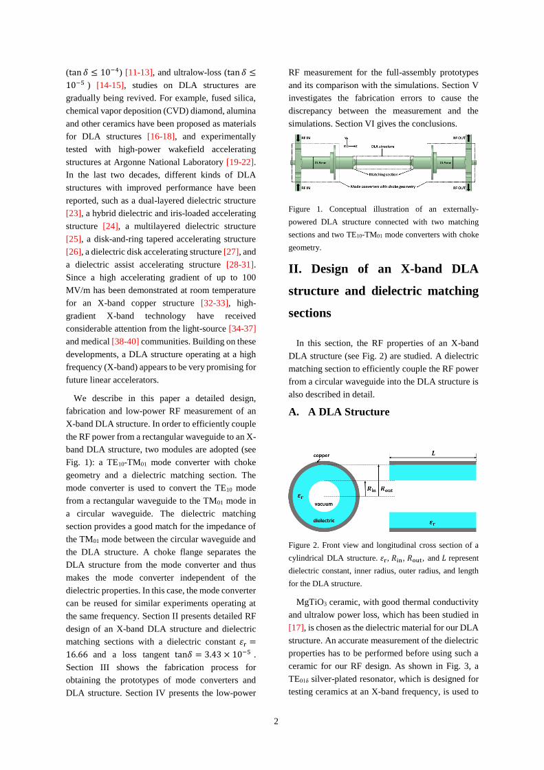
D. Tolerance Studies
Through previous studies, realistic geometrical
parameters for the dielectric matching section and
the DLA structure are obtained as follows:
휀r = 16.66, 𝑊1 = 2.035 mm, 𝐻2 = 2.74 mm, 𝜃 =
60o , 𝑅f = 2.0 mm, 𝑅m = 0.5 mm, 𝑅out = 4.6388
mm, 𝑅in = 3.0 mm, and 𝐿 = 100 mm. Using these
geometrical parameters, 𝑆11 = −54 dB and 𝑆21 =
−0.03 dB are achieved at an operating frequency of
11.994 GHz. The length of the DLA structure does
not have any effect on the S-parameters and RF-field
performance, so it is ruled out for tolerance studies
in this section. The tolerances of key geometrical
parameters (see Table 1) are discussed in detail.
Table 1. The tolerances of geometrical parameters for the
dielectric matching section and DLA structure.
𝑓0 = 11.994 GHz 𝑆11 ≤−30 dB
𝑆11 ≤−25 dB
𝑆11 ≤−20 dB
휀r = 16.66 [-0.079,
+0.081]
[-0.139,
+0.148]
[-0.24,
+0.27]
𝑊1 = 2.035 [mm] [-0.007,
+0.007]
[-0.012,
+0.012]
[-0.022,
+0.022]
𝐻2 = 2.74 [mm] [-0.015,
+0.017]
[-0.027,
+0.030]
[-0.051,
+0.054]
𝜃 = 60o [-2.5o,
+2.0o]
[-4.3o,
+3.7o]
[-7.3o,
+7.0o]
𝑅f = 2.0 [mm] [-0.042,
+0.040]
[-0.076,
+0.068]
[-0.140,
+0.120]
𝑅m = 0.5 [mm] [-0.061,
+0.049]
[-0.118,
+0.090]
[-0.245,
+0.151]
𝑅out = 4.6388
[mm]
[-
0.0076,
+0.0065
]
[-
0.0123,
+0.0127
]
[-0.020,
+0.025]
𝑅in = 3.0 [mm] [-0.006,
+0.007]
[-0.012,
+0.012]
[-0.024,
+0.020]
As we know, 𝑆21 for the realistic matching section
has a large 3 dB bandwidth of over 1 GHz, so it is
not sensitive to changes in the geometrical
parameters. The tolerances are studied by
calculating the dependence of 𝑆11 on the
geometrical parameters. By adjusting a certain
geometrical parameter from x to x ± dx, 𝑆11 is
calculated and compared with the setting
requirements of -30 dB, -25 dB, and -20 dB. As
shown in Table 1, 𝑆11 is very sensitive to 𝑊1, 𝑅out,
and 𝑅in and less sensitive to 휀r, 𝐻2, 𝜃, 𝑅f, and 𝑅m.
The dielectric fabrication accuracy should be better
than ± 0.02 mm in order to realize a 𝑆11 ≤ −20 dB,
which is still acceptable for efficient coupling.
E. A Full-assembly Structure
In this section, a full-assembly structure (see Fig.
9) is obtained by adding the DLA structure
connected together with two matching sections,
circular waveguides with the choke geometry, and
the TE10-TM01 mode converters. The mode
converters and choke geometry have been studied in
Refs. [48-49]. The RF performance of such a full-
assembly structure is described in detail. The whole
structure is simulated by analysing the electric field
distribution and S-parameters from Port 1 to Port 2.
RF power loss on both the metallic surface and in
dielectrics and accelerating fields in the vacuum
channel are also studied in detail.
(b)
Page 6
6
Figure 9. Electric field distribution for the full-assembly structure, where line MN is located on the centre along z-axis.
Figure 10. Simulated 𝑆11 and 𝑆21 as a function of
frequency for the full-assembly structure shown in Fig. 9.
Figure 10 gives calculated values of 𝑆11 = −40
dB and 𝑆21 = −0.67 dB for the full-assembly
structure at the operating frequency of 11.994 GHz.
Using the power density on the metallic surface and
in the dielectric area for an input power of 1.0 W, the
calculated RF power loss on the metallic surface is
𝑃loss_surface = 0.130 W and the RF power loss
obtained in dielectrics is 𝑃loss_dielectric = 0.012 W.
So the total RF power loss is 𝑃total_loss = 0.142 W.
The output RF power at Port 2 is 𝑃out = 0.858 W.
We thus achieve a transmission coefficient 𝑆21′ =
10 log (𝑃out 𝑃in⁄ ) = −0.67 dB, which agrees well
with the simulated 𝑆21 shown in Fig. 22. At the
maximum peak power of 40 MW from XBOX [50-
51] with a pulse width of 1.5 μs and a repetition rate
of 50 Hz an average input power of 3.0 kW will be
generated. The power loss on the metallic surface is
then 390 W and the power loss in dielectrics is 36 W.
A water cooling system is thus required for the high-
power test on the full-assembly structure.
Figure 11. Electric field magnitude along the line MN
shown in Fig. 9. The distance of point M is taken as 0 mm.
Figure 11 shows the electric field magnitude along
a line MN (see Fig. 9). The electric fields are
gradually becoming weaker, due to RF power loss in
the dielectric and on metallic surfaces, as the RF
fields propagate from point M to point N. The
average accelerating gradient is calculated to be
5773 V/m at an input power of 1.0 W. For a power
of 40 MW from XBOX, an average accelerating
gradient of 36.5 MV/m can be achieved for our DLA
structure.
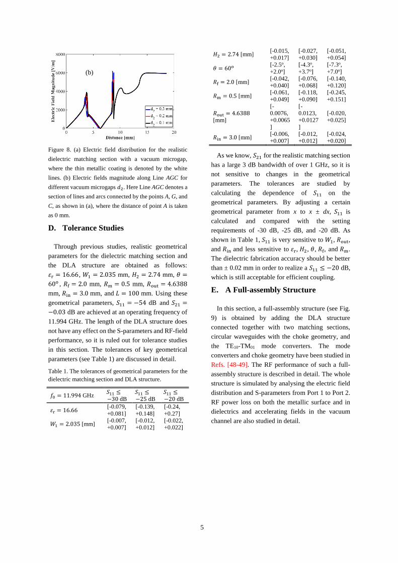
Figure 12 presents the full-assembly mechanical
design for the whole structure. The grey area denotes
the outer copper jacket, connected with openings to
avoid air trapping when pumping. Two conflat
flanges are used to connect the centre part with the
end parts, which are TE10-TM01 mode converters
with half-choke geometry.
Page 7
7
Figure 12. Full-assembly mechanical design for the whole structure, including a centre part and two end parts
III. Fabrication
A. TE10-TM01 mode converter with
half-choke geometry (end-part
prototype)
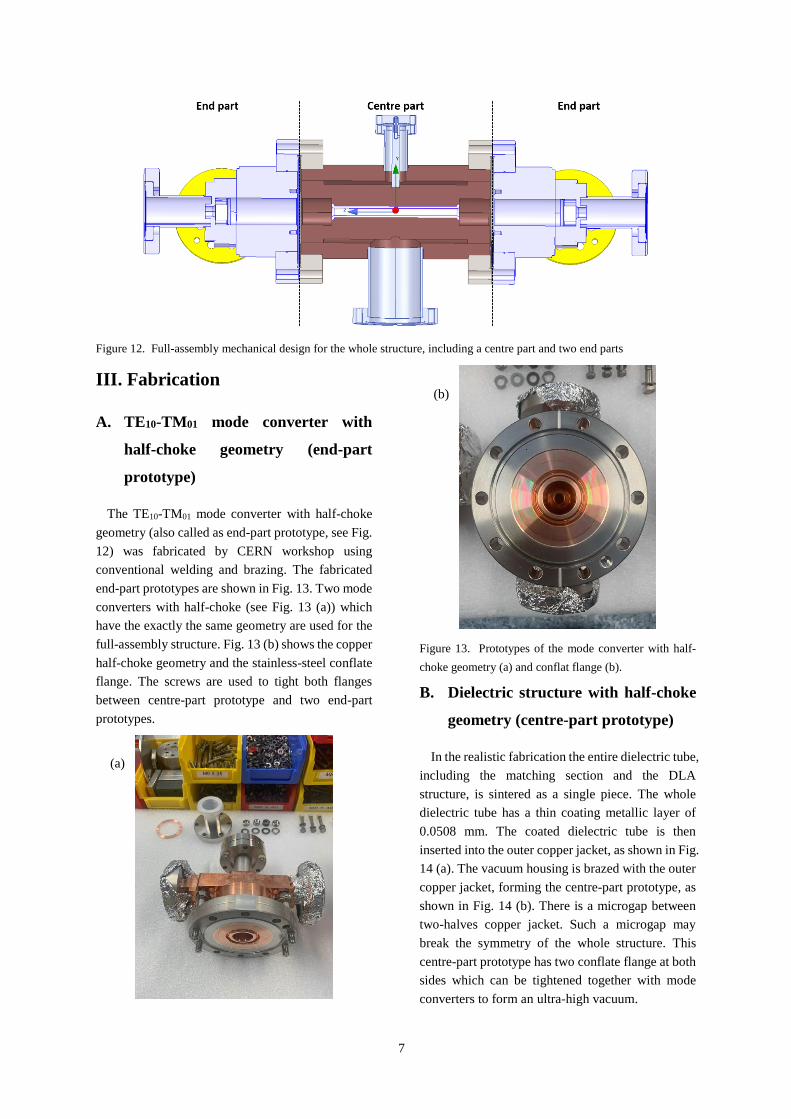
The TE10-TM01 mode converter with half-choke
geometry (also called as end-part prototype, see Fig.
12) was fabricated by CERN workshop using
conventional welding and brazing. The fabricated
end-part prototypes are shown in Fig. 13. Two mode
converters with half-choke (see Fig. 13 (a)) which
have the exactly the same geometry are used for the
full-assembly structure. Fig. 13 (b) shows the copper
half-choke geometry and the stainless-steel conflate
flange. The screws are used to tight both flanges
between centre-part prototype and two end-part
prototypes.
Figure 13. Prototypes of the mode converter with half-
choke geometry (a) and conflat flange (b).
B. Dielectric structure with half-choke
geometry (centre-part prototype)
In the realistic fabrication the entire dielectric tube,
including the matching section and the DLA
structure, is sintered as a single piece. The whole
dielectric tube has a thin coating metallic layer of
0.0508 mm. The coated dielectric tube is then
inserted into the outer copper jacket, as shown in Fig.
14 (a). The vacuum housing is brazed with the outer
copper jacket, forming the centre-part prototype, as
shown in Fig. 14 (b). There is a microgap between
two-halves copper jacket. Such a microgap may
break the symmetry of the whole structure. This
centre-part prototype has two conflate flange at both
sides which can be tightened together with mode
converters to form an ultra-high vacuum.
(b)
(a)
Page 8
8
It should be noted that the outer copper jacket
easily slides along the longitudinal direction inside
the vacuum housing. In this case, the choke gap 𝐿c
(see Fig. 18 in Ref. [48]) at both sides is changed
accordingly, which will be discussed in Subsection
D of Section IV. Therefore, a stainless-steel stick rod
is inserted into the groove of the outer copper jacket
in order to stop it from moving along the
longitudinal direction. This stick rod is integrated
with the flange outside the vacuum housing.
Figure 14. (a) The coated dielectric tube is put into the
outer copper jacket; (b) The assembly centre-part
prototype with the vacuum housing.
IV. Low-power RF measurement
In this section, low-power RF measurement is
performed for the full-assembly structure by using
the Vector Network Analyzer (VNA).
A. Assembly of two end-part prototypes
and an aluminium waveguide
In order to verify the measurement, an aluminium
waveguide is fabricated with an inner radius of
10.95 mm. The outer radius of this waveguide is the
same as that of the conflate flange. Such an
aluminium waveguide is assembled with two end-
part prototypes, as shown in Fig. 15 (a). A 4-port
VNA is used to measure this assembly structure.
Given that the symmetry of the assembly structure,
a quarter of the structure is modelled and simulated
in HFSS, as shown in Fig. 15 (b).
Figure 15. The realistic assembly (a) and simulation
modelling (b) of two end-part prototypes and an
aluminium waveguide.
The 4-port S-parameters can be transformed into
the 2-port S-parameters when the network has a
quarter symmetry. Figure 16 shows that the
measured 𝑆11′ = −34.4 dB and 𝑆21
′ = −0.26 dB
while the simulated 𝑆11′ = −57.9 dB and 𝑆21
′ =
−0.05 dB at the operating frequency of 11.994 GHz.
It is found that the measurements are different from
the simulations, which may be caused by fabrication
errors. However, the measured S-parameters are still
acceptable in terms of RF power transmission.
Therefore, it is concluded that most of RF power
propagates through the end-part prototypes in a
normal way.
(a)
(b)
(a)
(b)
Page 9
9
Figure 16. Comparison between simulated and measured
S-parameters.
B. Assembly of two end-part prototypes
and centre-part prototype
After confirming the end-part prototypes work
well, we move on to assemble two end-part
prototypes and centre-part prototypes together, as
shown in Fig. 17 (a). Figure 17 (b) shows the
modelling of the full-assembly geometry in HFSS
simulations, which will be used for comparing with
measurements.
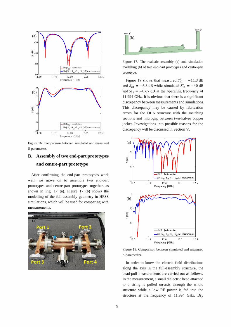
Figure 17. The realistic assembly (a) and simulation
modelling (b) of two end-part prototypes and centre-part
prototype.
Figure 18 shows that measured 𝑆11′ = −11.3 dB
and 𝑆21′ = −6.3 dB while simulated 𝑆11
′ = −40 dB
and 𝑆21′ = −0.67 dB at the operating frequency of
11.994 GHz. It is obvious that there is a significant
discrepancy between measurements and simulations.
This discrepancy may be caused by fabrication
errors for the DLA structure with the matching
sections and microgap between two-halves copper
jacket. Investigations into possible reasons for the
discrepancy will be discussed in Section V.
Figure 18. Comparison between simulated and measured
S-parameters.
In order to know the electric field distributions
along the axis in the full-assembly structure, the
bead-pull measurements are carried out as follows.
In the measurement, a small dielectric bead attached
to a string is pulled on-axis through the whole
structure while a low RF power is fed into the
structure at the frequency of 11.994 GHz. Dry
(a)
(b)
(a)
(a)
(b)
(b)
Page 10
10
nitrogen is fed into the structure to avoid permittivity
errors due to humidity changes. Electric field profile
can be obtained by calculating the change of
reflection coefficient with respect to the bead
position.
Based on Refs. [52-53], the square of electric field
strength 𝐸2 is proportional to the change of
reflection coefficient ∆𝑆 = 𝑆 − 𝑆0 , where 𝑆 is the
reflection coefficient and 𝑆0 is the zero-line fitting
function. Our full-assembly structure is a 4-port
network. The reflection coefficient 𝑆 = (𝑆11 +
𝑆13 + 𝑆31 + 𝑆33)/2 for Port 1 and Port 3 while 𝑆 =
(𝑆22 + 𝑆24 + 𝑆42 + 𝑆44)/2 for Port 2 and Port 4,
where 𝑆11 , 𝑆13 , 𝑆31 , 𝑆33 , 𝑆22 , 𝑆24 , 𝑆42 , 𝑆44 are
scattering parameters for our 4-port network. Figure
19 shows the measured electric field distribution on
the beam axis of structure at the operating frequency
of 11.994 GHz. The red curve denotes the electric
field distribution for the case of injecting RF power
from Port 1 and Port 3 while the blue curve denotes
the electric field distribution for the case of injecting
RF power from Port 2 and Port 4. The difference
between them demonstrates that the whole structure
is asymmetrical because of fabrication error and
microgap between two-halves copper jacket. It can
also be clearly seen that there are strong reflections
at the position of matching sections for both cases.
These reflections may also be caused by fabrication
errors for the matching sections, which will be
discussed in Section V.
Figure 19. Measured electric field magnitude for injecting
RF power from Port 1 and Port 3 (a), and from Port 2 and
Port 4 (b), respectively.
C. Add power splitters for the assembly
of two end-part prototypes and
centre-part prototype
In previous subsections, we know the fabrication
errors and microgap between two-halves copper
jacket may break the symmetry of the whole
structure. In this case, dipole TE11-type modes are
excited and propagate through the DLA structure in
our previous measurements. This may result in a
high power loss. In order to prevent the potential
dipole modes and remove the influence of microgap,
two power splitters are added into the RF
measurement.
At first, two power splitters are added for the
assembly of two end-part prototypes and an
aluminium waveguide. The 4-port network is
changed to a 2-port network. The low-power RF
measurement is carried out for this 2-port network,
as shown in Fig. 20.
Figure 20. The assembly of two end-part prototype and an
aluminium waveguide connected with two power splitters.
Figure 21 shows measured 𝑆11′ = 𝑆22
′ =
−26.1 dB and 𝑆12′ = 𝑆21
′ = −0.2 dB at the
operating frequency of 11.994 GHz. It can be clearly
seen that both 𝑆11′ and 𝑆12
′ agree well with 𝑆22′ and
𝑆21′ . This indicates that the power splitters are
symmetrical for RF propagating, thereby resulting in
a small reflection coefficient and negligible
transmission loss. In this measurement, dipole
modes are fully suppressed in the structure.
(a)
(b)
Page 11
11
Figure 21. Comparisons between measured (a) 𝑆11′ and
𝑆22′ , (b) 𝑆12
′ and 𝑆21′ .
After confirming that power splitters work
smoothly, we replace the aluminium waveguide
with the centre-part prototype which has a DLA
structure inside. As shown in Fig. 22, similar RF
measurements are carried out for this full-assembly
structure.
Figure 22. The full-assembly structure connected with two
power splitters.
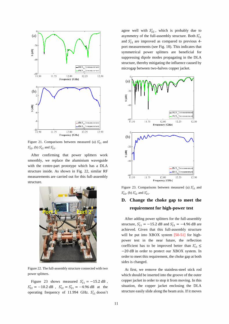
Figure 23 shows measured 𝑆11′ = −15.2 dB ,
𝑆22′ = −10.2 dB , 𝑆12
′ = 𝑆21′ = −4.96 dB at the
operating frequency of 11.994 GHz. 𝑆11′ doesn’t
agree well with 𝑆22′ , which is probably due to
asymmetry of the full-assembly structure. Both 𝑆11′
and 𝑆21′ are improved as compared to previous 4-
port measurements (see Fig. 18). This indicates that
symmetrical power splitters are beneficial for
suppressing dipole modes propagating in the DLA
structure, thereby mitigating the influence caused by
microgap between two-halves copper jacket.
Figure 23. Comparisons between measured (a) 𝑆11′ and
𝑆22′ , (b) 𝑆12
′ and 𝑆21′ .
D. Change the choke gap to meet the
requirement for high-power test
After adding power splitters for the full-assembly
structure, 𝑆11′ = −15.2 dB and 𝑆21
′ = −4.96 dB are
achieved. Given that this full-assembly structure
will be put into XBOX system [50-51] for high-
power test in the near future, the reflection
coefficient has to be improved better than 𝑆11′ ≤
−20 dB in order to protect our XBOX system. In
order to meet this requirement, the choke gap at both
sides is changed.
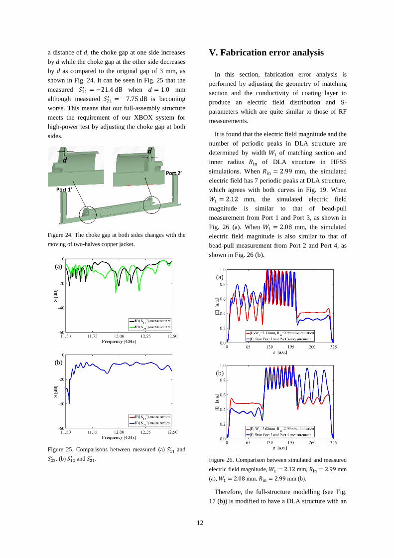
At first, we remove the stainless-steel stick rod
which should be inserted into the groove of the outer
copper jacket in order to stop it from moving. In this
situation, the copper jacket enclosing the DLA
structure easily slide along the beam axis. If it moves
(a)
(b)
(a)
(b)
Page 12
12
a distance of d, the choke gap at one side increases
by d while the choke gap at the other side decreases
by d as compared to the original gap of 3 mm, as
shown in Fig. 24. It can be seen in Fig. 25 that the
measured 𝑆11′ = −21.4 dB when 𝑑 = 1.0 mm
although measured 𝑆21′ = −7.75 dB is becoming
worse. This means that our full-assembly structure
meets the requirement of our XBOX system for
high-power test by adjusting the choke gap at both
sides.
Figure 24. The choke gap at both sides changes with the
moving of two-halves copper jacket.
Figure 25. Comparisons between measured (a) 𝑆11′ and
𝑆22′ , (b) 𝑆12
′ and 𝑆21′ .
V. Fabrication error analysis
In this section, fabrication error analysis is
performed by adjusting the geometry of matching
section and the conductivity of coating layer to
produce an electric field distribution and S-
parameters which are quite similar to those of RF
measurements.
It is found that the electric field magnitude and the
number of periodic peaks in DLA structure are
determined by width 𝑊1 of matching section and
inner radius 𝑅in of DLA structure in HFSS
simulations. When 𝑅in = 2.99 mm, the simulated
electric field has 7 periodic peaks at DLA structure,
which agrees with both curves in Fig. 19. When
𝑊1 = 2.12 mm, the simulated electric field
magnitude is similar to that of bead-pull
measurement from Port 1 and Port 3, as shown in
Fig. 26 (a). When 𝑊1 = 2.08 mm, the simulated
electric field magnitude is also similar to that of
bead-pull measurement from Port 2 and Port 4, as
shown in Fig. 26 (b).
Figure 26. Comparison between simulated and measured
electric field magnitude, 𝑊1 = 2.12 mm, 𝑅in = 2.99 mm
(a), 𝑊1 = 2.08 mm, 𝑅in = 2.99 mm (b).
Therefore, the full-structure modelling (see Fig.
17 (b)) is modified to have a DLA structure with an
(a)
(b)
(a)
(b)
Page 13
13
inner radius of 𝑅in = 2.99 mm, one matching
section with a geometry of 𝑊1 = 2.12 mm at one
side and the other matching section with a geometry
of 𝑊1 = 2.08 mm at the other side. The simulated
S-parameters are then obtained and compared with
the measured S-parameters. Figure 27 shows that
simulated 𝑆11′ = −11.8 dB is in good agreement
with measured 𝑆11′ = −11.3 dB but simulated
𝑆21′ = −0.97 dB is not consistent with measured
𝑆21′ = −6.3 dB at the operating frequency of 11.994
GHz. This means that the fabrication error on inner
radius is 0.01 mm which meets the requirement of
fabrication accuracy in subsection of tolerance
studies. However, the fabrication error on 𝑊1 for
one matching section is 0.085 mm and it is 0.045
mm for the other matching section.
Figure 27. Comparison between simulated and measured
S-parameters.
We continue investigating other possible reasons
to cause the inconsistence between the simulated
and measured 𝑆21′ . Besides the fabrication errors on
both 𝑅in and 𝑊1 , when the conductivity of thin
coating metal is changed to 𝜎 = 5.5 × 10⁵ , the
simulated 𝑆21′ = −6.25 dB is almost the same as the
measured 𝑆21′ = −6.3 dB at the operating frequency
of 11.994 GHz, as shown in Fig. 28. It is also found
that the simulated 𝑆11′ = −11 dB has a good
agreement with the measured 𝑆11′ = −11.3 dB at
the same frequency. This indicates that the whole
dielectric tube may have a poor quality of the coating.
Figure 28. Comparison between simulated and measured
S-parameters.
VI. Conclusions
This paper presented the design, fabrication and
low-power RF measurement of an X-band DLA
structure at CERN. In order to efficiently couple the
RF power from a rectangular waveguide to an X-
band DLA structure, the mode converters with
choke geometry and the matching sections were
carefully designed. Tolerance studies were also
carried out for the whole dielectric structure. A full-
assembly structure, including the DLA structure
connected with two matching sections, TE10-TM01
mode converters with choke geometry, was analysed
in detail.
A prototype of the DLA structure with the
matching sections was subsequently built and
mechanically assembled with the mode converters
for RF measurement. The mode converters were
demonstrated to propagate RF power in a normal
way. However, a significant discrepancy, due to
fabrication error, was found between measured and
simulated S-parameters. Geometrical analysis was
thus performed to understand the origin of these
differences. It was found that the fabrication error on
width 𝑊1 of the matching sections was the main
cause to dilute the reflection coefficient. The poor
quality of surface coating on the dielectric tube
resulted in a large attenuation for the transmission of
RF power. Through adjusting the choke gap, the
overall measured reflection coefficient 𝑆11′ =
−21.4 dB , which meets the requirement of our
XBOX system.
(a)
(b)
Page 14
14
In the next step, the whole structure will be put
into Xbox system for high power test. It is foreseen
that dielectric RF breakdown [20] and surface
resonant multipacting [19-20, 22, 54-55] would be
the primary issues to limit the achievable gradient in
DLA structures. Thus, further studies are also
required to solve these issues for the DLA structures
including using an applied axial magnetic field for
the whole structure. This will be reported in separate
publications.
Acknowledgments
The authors would like to thank Dr. Walter
Wuensch for the useful comments, Dr. Nuria
Catalan Lasheras, Serge Lebet, and Sergio Gonzalez
Anton for the mechanical and measurement support,
the team of Argonne Wakefield Accelerator facility
(Dr. Manoel Conde, Dr. John Power, and Dr.
Jiahang Shao, etc) for the fruitful discussions, and
Dr. Mark Ibison for his careful reading of the
manuscript.
References
[1] W. Gai and C. Ho, Modeling of the transverse mode
suppressor for dielectric wake‐field accelerator, J.
Appl. Phys. 70, 3955 (1991).
[2] E. Chojnacki, W. Gai, C. Ho, R. Konecny, S.
Mtingwa, J. Norem, M. Rosing, P. Schoessow, and
J. Simpson, Measurement of deflection ‐ mode
damping in an accelerating structure, J. Appl. Phys.
69, 6257 (1991).
[3] W. K. H. Panofsky and M. Bander, Asymptotic
Theory of Beam Break‐Up in Linear Accelerators,
Rev. Sci. Instrum. 39, 206 (1968).
[4] S. Frankel, TM0,1 Mode in Circular Wave Guides
with Two Coaxial Dielectrics, J. Appl. Phys. 18, 650
(1947).
[5] G. G. Bruck and E. R. Wicher, Slow Transverse
Magnetic Waves in Cylindrical Guides, J. Appl.
Phys. 18, 766 (1947).
[6] A. A. Oliner, Remarks on Slow Waves in
Cylindrical Guides, J. Appl. Phys. 19, 109 (1948).
[7] R. B. R.-Shersby-Harvie, A Proposed New Form of
Dielectric-loaded Wave-Guide for Linear Electron
Accelerators, Nature 162, 890 (1948).
[8] G. I. Cohn and G. T. Flesher, Design Construction
and Initial Operation of a Continuous Dielectric
Loaded Linear Accelerator, Electronics Research
Laboratories, Illinois Institute of Technology Report
2 (1952).
[9] R. B. R.-Shersby-Harvie, L. B. Mullett, W.
Walkinshaw, J. S. Bell and B. G. Loach, A
theoretical and experimental investigation of
anisotropic-dielectric-loaded linear electron
accelerators, in Proceedings of the IEE - Part B:
Radio and Electronic Engineering, vol. 104, no. 15
(1957), pp. 273-290.
[10] G. B. Walker and E. L. Lewis, Vacuum Breakdown
in Dielectric-loaded Wave-guides, Nature 181, 38
(1958).
[11] R. A. Woode, E. N. Ivanov, M. E. Tobar and D. G.
Blair, Measurement of dielectric loss tangent of
alumina at microwave frequencies and room
temperature, Electronics Letters 30, 2120, 1994.
[12] N. M. Alford and S. J. Penn, Sintered alumina with
low dielectric loss, J. Appl. Phys. 80, 5895 (1996).
[13] C. L. Huang, J. J. Wang, C. Y. Huang, Microwave
Dielectric Properties of Sintered Alumina Using
Nano-Scaled Powders of α Alumina and TiO2, J.
Am. Ceram. Soc. 90, 1487 (2007).
[14] A. Templeton, X. Wang, S. J. Penn, S. J. Webb, L.
F. Cohen, and N. M. Alford, Microwave dielectric
loss of Titanium Oxide, J. Am. Ceram. Soc. 83, 95
(2000).
[15] J. D. Breeze, X. Aupi, and N. M. Alford, Ultralow
loss polycrystalline alumina, Appl. Phys. Lett. 81,
5021-5023 (2002).
[16] W. Gai, Advanced Accelerating Structures and
Their Interaction with Electron Beams, AIP Conf.
Proc., 1086, 3 (2009).
[17] A. Kanareykin, New Advanced Dielectric Materials
for Accelerator Applications, AIP Conf. Proc., 1299,
286 (2010).
[18] P. Schoessow, A. Kanareykin, R. Gat, CVD
Diamond Dielectric Accelerating Structures. AIP
Conf. Proc., 1086, 398 (2009).
[19] J. G. Power, W. Gai, S. H. Gold, A. K. Kinkead, R.
Konecny, C. Jing, W. Liu, and Z. Yusof,
Observation of Multipactor in an Alumina-Based
Dielectric-Loaded Accelerating Structure, Phys.
Rev. Lett. 92, 164801 (2004).
[20] C. Jing, W. Gai, J. G. Power, R. Konecny, S. H.
Gold, W. Liu, A. K. Kinkead, High-power RF tests
on X-band dielectric-loaded accelerating structures,
IEEE Transactions on Plasma Science 33, 1155
(2005).
Page 15
15
[21] C. Jing, A. Kanareykin, J. G. Power, M. Conde, Z.
Yusof, P. Schoessow, and W. Gai, Observation of
Enhanced Transformer Ratio in Collinear Wakefield
Acceleration. Phys. Rev. Lett., 98, 144801 (2007).
[22] C. Jing, W. Gai, J. G. Power, R. Konecny, W. Liu,
S. H. Gold, A. K. Kinkead, S. G. Tantawi, V.
Dolgashev, and A. Kanareykin, Progress Toward
Externally Powered X-Band Dielectric-Loaded
Accelerating Structures, IEEE Transactions on
Plasma Science 38, 1354 (2010).
[23] C. Jing, A. Kanareykin, S. Kazakov, W. Liu, E.
Nenasheva, P. Schoessow, W. Gai, Development of
a dual-layered dielectric-loaded accelerating
structure, Nucl. Instrum. Methods Phys. Res., Sect.
A 594, 132 (2008).
[24] P. Zou, L. Xiao, X. Sun, W. Gai, T. Wong, Hybrid
dielectric and iris-loaded periodic accelerating
structure, J. Appl. Phys. 90, 2017 (2001).
[25] C. Jing, W. M. Liu, W. Gai, J. G. Power, T. Wong,
Mode analysis of a multilayered dielectric-loaded
accelerating structure, Nucl. Instrum. Methods Phys.
Res., Sect. A 539, 445 (2005).
[26] A. V. Smirnov, S. Boucher, S. Kutsaev, J. Hartzell,
E. Savin, Multi-cell disk-and-ring tapered structure
for compact RF linacs, Nucl. Instrum. Methods Phys.
Res., Sect. A 830, 294 (2016).
[27] J. Shao, C. Jing, J. Power, M. Conde, and D. Doran,
Study of a Dielectric Disk Structure for Short Pulse
Two-Beam Acceleration, in Proceedings of the 9th
International Particle Accelerator Conference,
IPAC2018, Vancouver, BC, Canada (JACoW,
Geneva, 2018), pp. 1539-1541.
[28] D. Satoh, M. Yoshida, and N. Hayashizaki,
Dielectric assist accelerating structure, Phys. Rev.
Accel. Beams 19, 011302 (2016).
[29] D. Satoh, M. Yoshida, and N. Hayashizaki,
Fabrication and cold test of dielectric assist
accelerating structure, Phys. Rev. Accel. Beams 20,
091302 (2017).
[30] S. Mori, M. Yoshida, D. Satoh, Multipactor
suppression in dielectric-assist accelerating
structures via diamondlike carbon coatings, Phys.
Rev. Accel. Beams 24, 022001 (2021).
[31] Y. Wei and A. Grudiev, Investigations into X-band
dielectric assist accelerating structures for future
linear accelerators, IEEE Transactions on Nuclear
Science 68, 1062-1071, (2021).
[32] S. Dobert, A. Grudiev, G. Riddone, W. Wuensch, R.
Zennaro, T. Higo, S. Matsumoto, K. Yokoyama, C.
Adolphsen, F. Wang, J. Wang, First high power tests
of CLIC prototype accelerating structures with
HOM waveguide damping, in Proceedings of the
25th International Linear Accelerator Conference,
LINAC2010, Tsukuba, Japan (KEK, Tsukuba,
Japan, 2010), pp. 208–210.
[33] T. Higo, Progress of X-band accelerating structures,
in Proceedings of the 25th International Linear
Accelerator Conference, LINAC2010, Tsukuba,
Japan (KEK, Tsukuba, Japan, 2010), pp. 1038–1042.
[34] G. D’Auria, X-band technology applications at
FERMI@Elettra FEL project, Nucl. Instrum.
Methods Phys. Res., Sect. A 657, 150 (2011).
[35] G. D’Auria, S. Di Mitri, C. Serpico, et al., X-band
technology for FEL sources, in Proceedings of the
29th International Linear Accelerator Conference,
LINAC2014, Geneva, Switzerland (CERN, Geneva,
Switzerland, 2014), pp. 101–104.
[36] A. Aksoy, Ö. Yavaş, D. Schulte, et al., Conceptual
design of an X-FEL facility using CLIC X-band
accelerating structure, in Proceedings of the 5th
International Particle Accelerator Conference,
IPAC2014, Dresden, Germany (JACoW, Geneva,
2014), pp. 2914-2917.
[37] A. Aksoy, A. Latina, J. Pfingstner, D. Schulte, Z.
Nergiz, Design optimization of an X-band based
FEL, in Proceedings of the 7th International Particle
Accelerator Conference, IPAC2016, Busan, Korea
(JACoW, Geneva, 2016), pp. 793-796.
[38] K. Dobashi, M. Uesaka, A. Fukasawa, et al., X-band
RF gun and linac for medical Compton scattering X-
ray source, AIP Conf. Proc., 737, 684 (2004).
[39] W. Wuensch, Applications of X-band and high-
gradient technology, CLIC Project Meeting, 5
December,2019(https://indico.cern.ch/event/86291
5/contributions/3636126/attachments/1956781/325
0679/CLIC_project_meeting_ww.pdf).
[40] Y. Lee, S. Kim, G. Kim, et al., Medical X-band
linear accelerator for high-precision radiotherapy,
Medical Physics 48, 5327-5342 (2021).
[41] A. Grudiev, W. Wuensch, A newly designed and
optimized CLIC main linac accelerating structure, in
Proceedings of the 19th International Linear
Accelerator Conference, LINAC2004, Lübeck,
Germany (Lübeck, Germany, 2004).
[42] R. Zennaro, A. Grudiev, G. Riddone, A. Samoshkin,
W. Wuensch, S. Tantawi, J. W. Wang, T. Higo,
Design and fabrication of CLIC test structures, in
Proceedings of the 23rd International Linear
Page 16
16
Accelerator Conference, LINAC2008, Victoria, BC,
Canada (Victoria, BC, Canada, 2008).
[43] A. Grudiev, W. Wuensch, Design of the CLIC main
linac accelerating structure for CLIC Conceptual
Design Report, in Proceedings of the 25th
International Linear Accelerator Conference,
LINAC2010, Tsukuba, Japan (KEK, Tsukuba,
Japan, 2010).
[44] H. Zha, A. Grudiev, V. Dolgashev, RF design of the
CLIC structure prototype optimized for
manufacturing from two halves, in Proceedings of
the 6th International Particle Accelerator
Conference, IPAC2015, Richmond, VA, USA, pp.
2147–2149.
[45] H. Zha and A. Grudiev, Design and optimization of
Compact Linear Collider main linac accelerating
structure, Phys. Rev. Accel. Beams 19, 111003
(2016).
[46] H. Zha and A. Grudiev, Design of the Compact
Linear Collider main linac accelerating structure
made from two halves, Phys. Rev. Accel. Beams 20,
042001 (2017).
[47] HFSS, www.ansys.com.
[48] Y. Wei, A. Grudiev, B. Freemire, and C. Jing, A
compact, low field, broadband matching section for
externally-powered X-band dielectric-loaded ac-
celerating structures, 2020. arXiv:2008.09203.
[49] I. Syratchev, Mode launcher as an alternative
approach to the cavity-based RF coupler of periodic
structures, CERN-OPEN-2002-005 (2002).
[50] N. Catalan-Lasheras, A. Degiovanni, S. Doebert, W.
Farabolini, J. Kovermann, G. McMonagle, S. Rey, I.
Syratchev, L. Timeo, W. Wuensch, B. Woolley, J.
Tagg, Experience operating an X-band high-power
test stand at CERN, in Proceedings of the 5th
International Particle Accelerator Conference,
IPAC2014, Dresden, Germany (JACoW, Geneva,
2014), pp. 2288–2290.
[51] A. V. Edwards, N. Catalan Lasheras, S. Gonzalez
Anton, G. Mcmonagle, S. Pitman, V. del Pozo
Romano, B. Woolley, A. Dexter, Connection of 12
GHz high power RF from the XBOX1 high gradient
test stand to the CLEAR electron linac, in
Proceedings of the 10th International Particle
Accelerator Conference, IPAC2019, Melbourne,
Australia (JACoW, Geneva, 2019), pp. 2960-2963.
[52] L. C. Maier Jr. and J. C. Slater, Field strength
measurements in resonant cavities, J. Appl. Phys. 23,
68 (1952).
[53] J. Shi, A. Grudiev, W. Wuensch, Tuning of X-band
travelling-wave accelerating structures, Nucl.
Instrum. Methods Phys. Res., Sect. A 704, 14 (2013).
[54] C. Jing, C. Chang, S. H. Gold, R. Konecny, S.
Antipov, P. Schoessow, A. Kanareykin, and W. Gai,
Observation of multipactor suppression in a
dielectric-loaded accelerating structure using an
applied axial magnetic field, Appl. Phys. Lett. 103,
213503 (2013).
[55] C. Jing, S. H. Gold, R. Fischer and W. Gai,
Complete multipactor suppression in an X-band
dielectric-loaded accelerating structure, Appl. Phys.
Lett. 108, 193501 (2016).