8/31/05 P.A. Semi, Inc. - Company Confidential 1 Design for Yield Using Statistical Design Fabian Klass Director of Technology and Manufacturing EE 380 Computer Systems Colloquium, Stanford University February 7, 2007
Transcript
8/31/05 P.A. Semi, Inc. - Company Confidential 1
Design for Yield Using Statistical Design
Fabian KlassDirector of Technology and Manufacturing
EE 380 Computer Systems Colloquium, Stanford UniversityFebruary 7, 2007
2
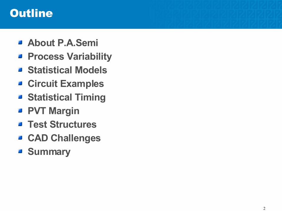
Outline
About P.A.SemiProcess VariabilityStatistical ModelsCircuit ExamplesStatistical TimingPVT MarginTest StructuresCAD ChallengesSummary
3
About P.A. Semi
Santa Clara-based fabless processor companyPower ArchitectureTM Licensee
Design our own Power Architecture processorsOnly 3rd company after IBM and Freescale
Noted industry veterans combine in 150-strong organizationVenture backed by Bessemer, Venrock, and Highland CapitalCurrently engaged with over 100 customers across different market segments
Strategically partnered with IBMBreakthrough processor solution focused on low power @ high performance
Scalable 64-Bit Power multicore architectureRedefines high performance (2GHz) at ultra low power (4W) 39 patents filed and 11 more patents in progress towards filing
4
ComputeServer Blades
DigitalEntertainment
EmbeddedBoards Routers
Switches
WirelessBasestations
StorageSystems
ImagingSystems
GamePlayers
Critical RequirementsPower Efficiency High Performance
Three main reasons why process variability has become so important:
Moore's law:Exponential growth in device integrationBillions of devices per die in 65nm and beyond
Shrinking devices:Gate oxides approaching a few AngstromsFewer dopants under the gate (~102)
Ultra low VDD:VDD scaling < 1V to manage power.Vt not scaling, limited by leakage.Less headroom, more sensitivity to ∆Vt.
7
Process Variation
Global: die-to-die, wfr-to-wfr, and lot-to-lot variations caused by changes in:
Tox Xtor W & L N/PWELL doping N/PMOS flatband voltage Stress-induced effects
Local: within-the-die variations caused by:
Xtor W & L mismatch Vt mismatch ACLV
Global
Local
8
Width and Length Mismatch
Caused by variations in the lithographic processWidth and Length variations are uncorrelatedSmall transistors more sensitive to W/L changes
Intel 65nm 6T SRAM cell
65nm CMOS NAND cell
9
Vth Mismatch
Random fluctuations due to relatively small number of dopants in the channelVth variance is inversely proportional to transistor areaPelgrom's Law:
Source: Asenov A. “Random Dopant Induced Threshold Voltage Lowering and Fluctuations in Sub-0.1 umMOSFET's: A 3-D 'Atomistic' Simulation Study” IEEE Trans. On Electron Devices, Vol 45, No 12, Dec 1998
Vth=0.78V
Vth=0.56V
170Dopants
V th=K /W×L
10
Statistical Models
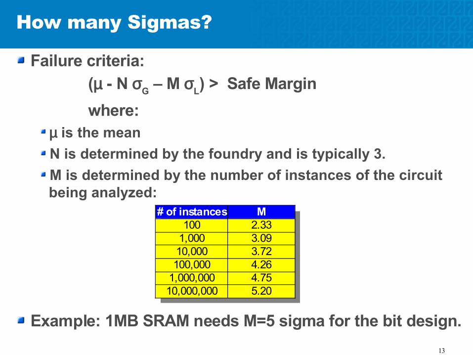
Provided by most foundriesMore realistic than corner models.Cover the full design space.Foundries typically offer a 3σ process.The number of local sigma is determined by the designer.
SS
TT
SF
FS
PMOS
NMOS
σG (Global)
σL (Local)
123
1
4 5
243
FF
11
Monte Carlo
Monte Carlo involves simulating a circuit over a wide range of randomly chosen devices parametersThe result is a distribution plot of design constraints, e.g., delay or noise marginTypically tens of thousands simulations needed, including Vdd and Temp sweeps
3.0
2.8
2.6
2.4
2.2
2.0
1.8
1.6
1.4
1.2
1.0
0.8
0.6
0.4
0.2
0.0
-0.2
-0.4
-0.6
-0.8
-1.0
-1.2
-1.4
-1.6
-1.8
-2.0
-2.2
-2.4
-2.6
-2.8
-3.0
0.000
0.100
0.200
0.300
0.400
Delay
Dis
trib
utio
n
Vth
Del
ay
12
When to use statistical analysis
Usage limited to process-sensitive circuits: Races Contention Mismatch
Run Monte Carlo Plot passing ratio vs. ∆Vin Find µ & σL for sensamp Find µ & σL for SRAM Iread Min VDIFF:
-200 -150 -100 -50 0 50 100 150 2000%
10%
20%
30%
40%
50%
60%
70%
80%
90%
100%
Delta Vin [mV]
PASS
σSA
V DIFF=SA
1−M× IREAD / IREAD2
16
Other Circuits
Other possible applications for statistical circuit design: Dynamic logic Latches Register files cells Pulsed flops Level shifters Analog circuits
Advantages: All circuits designed to a target sigma Avoid weak links Avoid overdesign
17
Statistical Timing
Each gate has a mean and sigma. Sigmas can be computed using Monte CarloThe sigma of a path is determined by adding (i.e., sum-square) the sigmas of individual gates
σ1
σ2
σn
Critical Path
Path= 12 2
2... n2
18
Speed Distribution
Each chip has a local distribution on top of the global distribution due to local variationsNot all parts within a [+3σ, -3σ] window will yield above target due to local variations
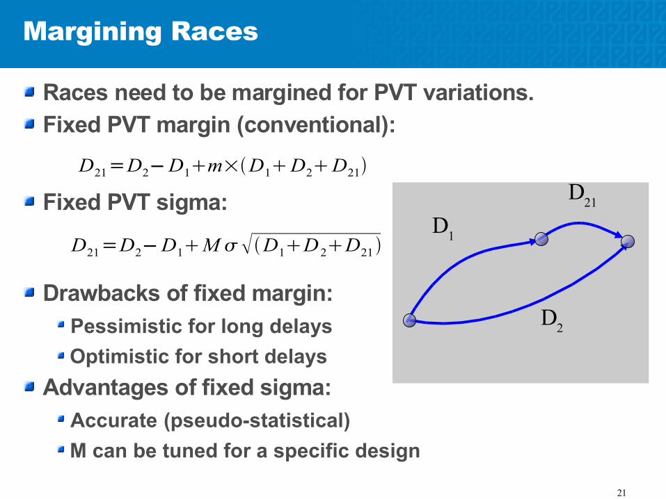
Races need to be margined for PVT variations.Fixed PVT margin (conventional):
Fixed PVT sigma:
Drawbacks of fixed margin: Pessimistic for long delays Optimistic for short delays
Advantages of fixed sigma: Accurate (pseudo-statistical) M can be tuned for a specific design
D1
D2
D21
D21=D2−D1m×D1D2D21
D21=D2−D1M D1D 2D21
22
Margining Races (cont.)
Fixed sigma: PVT margin varies with the logic depth PVT margin varies with Vdd
1 2 3 4 5 6 7 8 9 10 11 12 13 14 15 16 17 180.0%
10.0%
20.0%
30.0%
40.0%
50.0%
Logic Depth
PVT
Mar
gin
[%] Lower
Vdd
23
Measuring Process Variability
Test structures were developed to measure process variability.A testchip was built in a 65nm, triple-Vt, dual-oxide CMOS process.Data was collected across dies, wafers, lots, and across voltage and temperature.Measured data was used to:
A Racer circuit measures on-die process variations in Si.> 100 copies of the Racer module are placed across the die.
The spread in the location of the leading “1” provides an indication of the process variability.
clk
FF
XOR/XNOR
clk_en
select_0_Lselect_1_L
CKG
10
0
1
1
1
0
0
1
1
0
0
0
FF
FF
FF
FF
FF
FF
FF
FF
FF
MUX MUX
CKG
FF1/2
2 4 6
25
Racer Results
Racer data shows large spreads at low Vdd. Data can be used to predict circuit yield across Vdd.Low Vdd is the yield limiter!
Low
er V
dd
Bar Chart
Binned Inverter Count0 1 2 3 4 5 6 7 8 9 10
0200400600800
1000
0200400600800
1000
0200400600800
1000
0200400600800
1000
0200400600800
1000
0200400600800
1000
#Inverters3% 6% 8% 10% 11% 13% 14% 15% 17%
0%
25%
50%
75%
100%Yield @ 4 Sigma
#Inverters
Yiel
d
Lower Vdd
26
A Leaker Circuit
A Leaker circuit measures leakage spread (Ioff/Ion) in Si.It measures Ioff/Ion by sensing a tied-off skewed inverter with a 2P:1N inverter and latching to a flop.Multiples copies of the leaker module are placed on the die.Separate modules are used for standard Vt, low Vt, and high Vt devices.
1
1
0
1
0
FF
FF
FF
FF
FF
LK
clk
LK
LK
LK
LK
WP
WN
WN
2xWN
1024xWN
512xWN
27
Leaker Results
Leaker data was collected across voltage and temperature.Distributions were generated and µ/σ data was obtained.Ioff/Ion ratio worse at low Vdd for all Vt devicesIoff/Ion ratio worse at high temperature for all Vt devices
0.66V 0.76V 0.91V 1.1V0.0
2.0
4.0
6.0
8.0
10.0
12.0
14.0
16.0
18.0
20.0
IOFF/ION RATIO MEAN + 4 SIGMA
HVTSVT LVT
VDD
IOFF
/ION
RAT
IO [L
og2]
0 1 2 3 4 5 6 7 8 9 10 11 120
5
10
15
20
25
30
35
40
45
50IOFF/ION RATIO
HVTSVTLVT
IOFF/ION RATIO (Log2)
DIS
TRIB
UTI
ON
SafeMargin
28
CAD Challenges
Applications for statistical design:TimingPowerERCReliability
Main Challenges:Run time: Running Monte Carlo on a library would take years!Tools need to be 'context aware': Ex:Timing optimization depends on the shape of the timing histogram
Pseudo-statistical approachUsing statistical methods without running Monte Carlo.
29
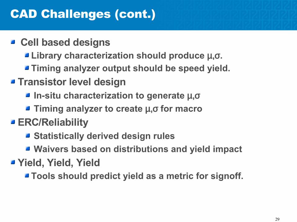
CAD Challenges (cont.)
Cell based designsLibrary characterization should produce µ,σ.Timing analyzer output should be speed yield.
Transistor level designIn-situ characterization to generate µ,σTiming analyzer to create µ,σ for macro
ERC/ReliabilityStatistically derived design rulesWaivers based on distributions and yield impact
Yield, Yield, YieldTools should predict yield as a metric for signoff.
30
CAD: What's missing
Tool IntegrationIntegration of DFM and DFY tools to predict:
ValidationValidation of DFY tools in SiliconJustification of investment
31
Summary
Ignoring process variability may lead to non-functional designs or suboptimal yields.DFY will become more relevant as Vdd continues to scale and device geometries keep shrinking.Circuit solutions alone will not be sufficient if Moore's law continues.Process variability need to be handled at higher levels of the design processFuture designs will incorporate:
Thank YouThe P.A. Semi name and the P.A. Semi logo and combinations thereof are trademarks of P.A. Semi, Inc.
The Power name is a trademark of International Business Machines Corporation, used under license therefrom.SPECint and SPECfp are registered trademarks of the Standard Performance Evaluation Corporation (SPEC).
All other trademarks are the property of their respective owners.


![Computational Insights and the Theory of Evolutionweb.stanford.edu/class/ee380/Abstracts/120425-slides.pdfBefore Darwin • Charles Babbage [Paraphrased] “God created not species,](https://static.documents.pub/doc/80x56/5f16f2cd0844e33b5013cf7e/computational-insights-and-the-theory-of-before-darwin-a-charles-babbage-paraphrased.jpg)