33

A Design System for RFIC:
Challenges and Solutions
Paolo Miliozzi, Ken Kundert y,
Koen Lampaert, Pete Good and Mojy Chian
Conexant Systems, Inc., Newport Beach, CA
y Cadence Design Systems, San Jose, CA
Abstract
The past few years have witnessed an explosion of interest in radio frequency integratedcircuits (RFIC's). The expansion of the market for wireless communication devices hasgiven a tremendous push to the development of a new generation of RFIC products, wheremore and more functions are integrated on the same chip. In this fast-growing environmentwhere time-to-market constraints force tight schedules, having a good design methodology,innovative CAD tools and a well-integrated design system are key factors to success.
In this paper, we describe a Design System developed to provide the designer witheverything necessary to accurately predict the behavior of RFIC devices, including layoutand package parasitic e�ects. We show the importance that a well-de�ned and integratedsystem has on the �nal goal of obtaining a manufacturable design that meets speci�cationsat minimum cost and in the minimum time. A close link between schematic, models andlayout is of paramount importance to ensure the accuracy needed for RF design. We givean overview of the advanced methods and tools currently available for simulation and noiseanalysis of RF devices. Finally, we show a couple of design examples that have obtained�rst-silicon success.
1 Introduction
In recent years, RF design has undergone a paradigm shift as more and more RF functions have beenintegrated on a single chip and the number of discrete components has decreased. Traditional discretedesigns are quickly reaching the physical limits of size, parasitics, and electrical performance. Moreover,while in the past the wireless market was dominated by the relatively slow-growing military and cabletelevision industries, its new consumer nature forces designers to seek more integrated solutions asopposed to the bulky, expensive, and power-hungry ones previously developed.
Being able to place many RF and IF subsystems on the same die promises dramatically smallersize, greater manufacturability, higher performance, and lower power consumption. This trend is moreevident in the low-power segment of the wireless communications market, which includes handsets forcordless and cellular phones, pagers, and the more recent BlueTooth standard (See paper in thisissue), where more compact solutions are needed to accommodate the ever-growing demand for lighterand cheaper products. Even though RF designs contain fewer devices compared to digital chips, theyare inherently more challenging as very little automation is available for the design process. Moreover,
1

RF devices are typically pushed to their performance limits, thus all the non-linearities and secondorder e�ects need to be taken into account.
Consider, as an example, the Super-Hetherodyne transceiver depicted in Figure 1. This transceiveris the combination of several integrated circuits built using di�erent techonologies: bipolar, GaAsand ceramic SAW �lters are used for the RF section, bipolar for the IF section and CMOS for base-band. This design partitioning is now starting to change thanks to technology advances that make itpossible to extend the range of usability of the less expensive CMOS technology. A good overview ofthe technology choices for RFIC can be found in [1].
Historically, IC and RF designers have used di�erent design methodologies, tools and practices.Traditional analog designers have enjoyed an integrated front-to-back IC design system. On the otherhand, RF designers, with a discrete design background, have used board-level CAD design tools. WithIC applications approaching several GHz, and the appeal of monolithic design because of the growingdevice speed, silicon is bridging the gap between traditional low-frequency analog design and discreteRF design, bringing the 2 worlds to converge in order to provide a better and cheaper solution forconsumers.
Many of the limitations of IC processes are well known. These involve the inability to economicallyintegrate high value capacitors and resistors, relatively poor (typically> 10% ) absolute error tolerancesof component parameters, and limited choice of device types. In addition to these limitations, the RFICdesigner must also be concerned with parasitics associated with the substrate, the general lack of highquality passive components, and package parasitics.
Moreover, tight schedules imposed by severe time-to-market constraints, make prototyping impos-sible and urge designers to seek validation of their design from accurate and extensive simulation.
In order to overcome all these problems, RF designers must rely on a Design System that allowsthem to accurately predict the behavior of their devices under their normal working conditions.
The paper is structured as follows: Section 2 gives an overview of the parts that compose a DesignSystem for RF and focuses on the importance that e�ective synchronization and coordination betweendi�erent contributors has for the success of a design. In Section 3 the issues involved in device modelingfor RF are described. An in-depth overview of the various simulation methods currently available (e.g.spice, shooting-methods and harmonic balance), is given in Section 4. Section 4 also addresses thesubject of noise analysis. This is an area where CAD tools can play a major role helping designersreduce their margins and obtain better performance with lower power consumption.
In Section 5, techniques to automate the layout generation of devices are described. Also, amethodology is presented to retarget a design (template) from one set of specs to another and fromone technology to another. In Section 6 the importance of keeping a very tight link between what issimulated and what is laid out so that pre- and post-layout simulations track each other is underlined.
Finally, in Section 7 we show a couple of RFIC designs that have gone through the design cycleand obtained �rst-pass silicon success as a result of accurate process characterization, noise prediction,device & package models, and appropriate simulation engines in this Design System.
2 Design System
ADesign System provides the designer with a comprehensive set of tools, libraries and methodologiesthat cover an entire design ow. Moreover it is a framework within which process developers, devicemodeling people, IC designers, package developers and layout designers can exchange informationand interact with one another for the common goal of minimizing both the power consumption andtime-to-market of every design.
We can divide a Design System in the following main components:
2
� Design Environment;
� Design Kits;
� Design Methodology associated with a Tool Flow;
Synchronization, testing and release mechanisms are very important aspects of a Design Sys-
tem and its components.A wide portfolio of communication systems has very di�erent technology requirements. To imple-
ment the transceiver shown in Figure 1 many di�erent technologies are needed. Hence, many processesneed to be managed which may be at di�erent stages of their development. Some of them may bevery mature and require very little or no modi�cations. When working on applications that require acutting-edge process, the process development and design are done concurrently. This has the advan-tage that complex test circuits can be available at early stages of the process development, providingfeedback for the �ne tuning of process parameters. In these cases, since the process is not yet stable,many changes may take place during the design. These changes need to be passed on to designersin a timely manner while keeping the design system consistent. In order for this type of concurrentengineering to be succesful, it is very important to have synchronization mechanisms in place betweencontributors. This is one of the main factors behind the success or the failure of a design.
Most of the time, a complex design is not carried out by a single design team, but rather by manydesign teams working in di�erent geographical locations and even di�erent time zones. In these casesthe importance of having a common Design System is clear. Since the data structure is the sameeverywhere, synchronization among all sites can be easily accomplished by broadcasting nightly thechanges that have occurred.
2.1 Design Environment
De�ning a common design environment is necessary to allow seamless interaction between users andtools and between one tool and another. This has the added advantage that exchanging designsamong groups becomes much easier. Since intellectual property (IP) reuse is becoming a key factorin achieving rapid development of new products to meet time-to-market constraints, having an easyway to leverage on the IP portfolio is very important. Design reuse, especially in the case of softIP, is greatly facilitated by the existence of a common design environment throughout a company.The design environment provides standard setup and initialization �les, a common data structure fordesign data and technology data, a revision control mechanism, an easy way to select tool and designkit versions and several layers of software.
The standard setup and initialization �les allow users to concentrate on the design. Since thesystem is integrated and has a standard con�guration, most of the information needed to run toolscan be pre-�lled out, hence reducing the overhead for the users. Well-de�ned directory structures andnaming conventions are the basis for a good design environment.
Revision control mechanisms are useful when the design is carried out by a large number of people.The usage model calls for a central repository, or vault, and individual work areas. The most commonfeatures provided by these systems are: (1) only one person at a time can access for edit a piece ofdesign data (check out with lock); (2) a commented history of all the modi�cations for each cell isautomatically maintained and can be accessed by any user; (3) as soon as a modi�ed piece of data ischecked in into the vault, it can be seen and used by any other person subscribed to that project.
Another important book-keeping mechanism for a project is to maintain a con�guration �le insidethe project area to keep track of tool and Design Kit versions used to do the speci�c design. Thisallows you to capture a snapshot of the environment for future comparisons between simulation data
3

and measurements, since the design system may have evolved after the design data was released forfabrication.
Software is developed to perform many di�erent tasks within a design system: to add featureswhich are not available by default in the o�-the-shelf version of the tools; to post-process tools outputdata for presentation purposes or for use by a down-stream tool of the supported ow; to calculatederived parameters to be shown to designers; etc.
While providing all the default settings needed to use theDesign System, the environment must beopen in order to allow customization and accomodate the needs of expert users and other requirements.For example a speci�c project may need special versions of tools and/or design libraries; users mayhave preferences in the way their data is displayed, etc.
2.2 Design Kit
At the core of the Design System is the Design Kit. This is a collection of objects that enable thedesigner to use a speci�c process. Hence, while all the other parts of the system are common for allprocesses, anything that is technology-speci�c is part of the Design Kit.
A Design Kit is composed of a technology library which contains all the primitive componentsavailable for a speci�c technology. Each component is fully characterized both electrically and physi-cally. From the electrical point of view this means that models are available for all supported simulators.Nominal models are available as well as a number of corner cases to capture the statistical variation ofprocess parameters. Both modeling and layout issues for low-power RF are topics of forthcoming sec-tions(see sections 3 and 5). To make sure that the model being simulated corresponds to the structurethat is going to be laid out, a set of routines are written to calculate the appropriate layout featuresof the cell, based upon the electrical values requested by the users. These same values are then passedto device generators that build the physical geometries using all the appropriate layers.
Finally, rule �les for all the various layout veri�cations and for parasitic extraction provide the lastpiece of information necessary to close the loop before submitting the data for fabrication. AdvancedLVS rules have been written to ensure not only that electrical equivalence is achieved, but also thatthe layout is realized exactly according to the parameters speci�ed on the schematic. The reason fordoing this is discussed in Section 3. Hence LVS checks must include veri�cation of parameters like thenumber of �ngers for multi-�nger FETs, the presence of substrate contacts close to the devices, etc.
2.3 Design Methodology and Tool Flow
A Top-Down, Schematic-Driven Design Methodology is proposed in thisDesign System where all theinformation to drive simulators and layout generators is speci�ed on the schematic. Figure 2 depictsthe Design Flow.
At the top of the block diagram, the tool for capturing the design can be found. As we discussedin Section 2.1, the philosophy of having a common design environment calls for maintaining onlyone schematic capturing tool. The tool can then be integrated with a set of simulators which performdi�erent types of simulations according to the application. Some of the simulators are tightly integratedwith the schematic allowing the usage of the schematic itself to cross-probe the simulation results. RFsimulation-speci�c issues are covered in great detail in Section 4.
Schematic and layout editors are tightly integrated through the usage of layout generators. Anycomponent parameter can be changed at any time during the design process and the change can bepropagated from the schematic view to the layout view and viceversa. Also, connectivity informationis available in the layout tool, thus reducing almost to zero the probability of making mistakes in the
4

routing phase. The graphical information provided about connectivity helps during the placementphase as well. Other sophisticated tools developed in-house allow us to migrate designs from onetechnology to another, as described in Section 5.
The integration of layout and veri�cation tools allow layout designers to quickly check the correct-ness of the layout interactively while working on it. All the checks are available through menu picks.Layout engineers can decide whether to use their local machine for small veri�cation jobs or submitthem to computer servers.
Once the layout is completed, several steps are required before the data is validated. First a DesignRule Checking is performed to ensure that the layout conforms to all manufacturing speci�cations.Then a Layout Versus Schematic check is run to ensure electrical equivalence between layout andschematic.
Finally, a parasitic extraction is performed and the whole circuit is re-simulated. If the circuit istoo large, it may not be possible to simulate the whole thing at transistor level. In this case behavioralmodels can be written for less sensitive blocks and they can be used together with the extracteddescription of other blocks to carry out the simulation. With the advent of System on Chip, behavioralmodeling is becoming more and more important for analog and RF devices.
3 Modeling for RF
One of the most important capabilities that a Design System has to provide is the transfer ofaccurate information about device performance from the silicon to the designer. Simulation resultscan only be as accurate as the models used to mathematically describe the physical behavior of thedevices. Therefore, a very important part of a design system is the accuracy of the models. In thissection we will analyze some of the issues encountered when modeling the behavior of some passiveand active integrated components for RF applications.
3.1 MOS transistor
Digital applications have been the major driver for the development of the CMOS technology. As aconsequence, most of the research e�orts on MOS modeling have been focused towards digital design.
Advances in lithography allow us to build MOS devices with shorter channel lengths operatingat lower voltages. As device geometries shrink to deep submicron dimensions, circuit performance ispushed to the limits of process capability and MOS transistors are used for high frequency applicationsin places where BJTs were previously the only viable candidates.
The main goal in digital design is to apply the principles of scaling to obtain higher switching speedand lower power dissipation [2]. In addition to these performance requirements, RFIC designers haveto deal with other issues like noise, gain, linearity and e�ciency.
Throughout the years MOSFET models have evolved from very simple physics-based analyticalmodels (e.g. spice level 1,2,3) [3] to more empirical ones (e.g. BSIM2, Hspice level 28) with many non-physical parameters to better �t measurement data. However, recently introduced models are based onmore advanced device physics and have physically-meaningful model parameters, e.g. Phillips MOS 9,BSIM3v3 [4, 5] and EKV [6, 7]. Originally, most of the model development was done to achieve a good�t for DC characteristics while the main requirement for the capacitance model was good continuityrather than good �t. The new frequency regimes, in which MOS transistors are now employed, putmore demand on the accuracy of the AC part of the MOSFET model in addition to the DC one, bothrequiring careful validation of the extracted model parameters. Although BSIM3v3 is the de facto
public-domain industry standard MOS model, it has limitations when approaching a few GHz, giving
5
inaccurate results. The same is true for all the compact models currently available, which need to beenhanced to predict correct RF behavior. In order to do that, the modeling expert is presented withtwo choices:(1) develop new compact models and ask tool vendors to implement them within theirsimulators; (2) develop composite models, augmenting existing models to extend their capabilities.From a Design System perspective it is better to keep the intrinsic model standard so that it wouldbe available in all simulators, and then add extra components to achieve a better agreement withmeasurements. To check for the validity of the high-frequency portion of the composite model, S-parameter measurements are used.
The main e�ects that need to be accounted for and that are not present in standard MOS modelsare:
� Terminal resistances, in particular the gate, both for their resistive and noise contributions;
� Signal coupling through the substrate within the device and between devices;
In Figure 3 the cross-section of the MOS transistor and all its parasitic components are shown [8].Drain and source diodes are pulled out of the intrinsic model in order to have access to the internaldrain and source nodes. A comprehensive treatment on the subject of MOS Modeling with thoroughanalyses of the latest models can be found in [9].
Figure 3 also shows a compact scaleable model that has been derived and implemented for Spicesimulation as described in [8, 10]. This model is based on the quasi-static approximation and it wasfound to provide simulation results in good agreement with measurements up to about 10GHz [8].
Using this simple equivalent circuit has several advantages over more complicated ones that takeNon-Quasi-Static e�ects into account. First of all, simulation time is not compromised since only afew nodes are added; second, a simpli�ed set of equations can be derived from it to analytically relatethe values of the extrinsic and intrinsic components with the Y-parameters.
y11 =j!Cgg
1 + j!RgCgg
(1)
y12 =�j!Cgd
1 + j!RgCgg
(2)
y21 =gm � j!(Cm + Cgd)
1 + j!RgCgg
(3)
y22 =gds + j!(Cdb + Cgd)
1 + j!RgCgg
(4)
where Cgg represents the total gate capacitance, Rg the gate resistance, Cgd the total gate-to-draincapacitance, Cdb the total drain-to-bulk capacitance, Cm the transcapacitance that represents thenonreciprocal capacitance e�ect between gate and drain, gm the transconductance and gds the outputconductance.
S-parameter measurements carried out on the MOS transistor biased in its linear region of oper-ation are then used for a direct extraction of the RF model parameters, as presented in [8]. Finally,de-embedding techniques are applied to separate the device contributions from the ones due to themeasurement setup and surrounding environment [11].
The care with which RF device models are extracted suggests that every parameter is highly criticaland that to get good agreement between simulated and manufactured devices,
To achieve good agreement between simulated and measured devices, the RF model must be ex-tracted with great care and the design system must be very well controlled. Consider the case of sizinga MOSFET: W and L alone are not enough to fully characterize the electrical behavior of your
6
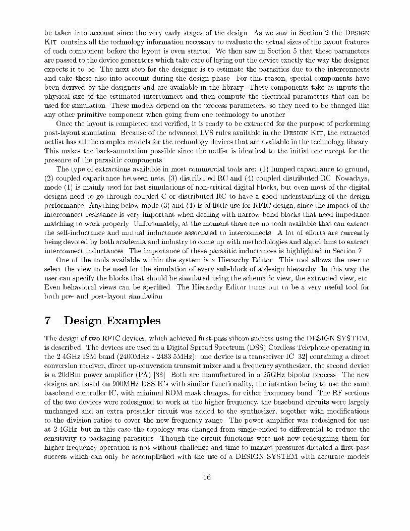
device. You also need to know the number of �ngers used for the gate, the location of the substratecontacts, etc. It is clear from the measurements that all of these parameters greatly a�ect the deviceperformance [10]. Consider the example of a MOS transistor laid out with an even number of �ngersand one for which an odd number of �ngers has been used. Figure 4 shows the di�erence betweenthese two devices. Although the total width and length are the same for the two devices, area andperimeters of drain and source di�er in the two con�gurations. This can be a desired e�ect: designerscan assign a bigger area to the source when it is connected to ground, for example. By doing this theycan obtain a higher driving current without increasing the drain-to-bulk parasitic capacitance. Thisyields two considerations: �rst, the device is no longer symmetrical, but one of the two terminals hasmore di�usion-to-bulk parasitics associated with it; second, the intra-device substrate resistive pathsfrom di�usion to the bulk contacts are di�erent in the two cases. The model needs to be aware of thisdi�erence in order to correctly predict the device behavior.
Another important aspect of the transistor model is to accurately predict the noise behavior. Asit will be made clear later, there is a direct relationship between power dissipation and noise in RFdesign. Hence, the more accurate the noise prediction, the less over-design is necessary. There aremany sources of noise within a MOS transistor: noise at the drain due to both channel thermal noiseand icker noise; thermal noise due to the terminal resistances and to substrate resistance, see [10].
3.2 Bipolar
The bipolar junction transistor (BJT) is still dominates the RFIC domain. It has better performancethan the MOSFET and has a signi�cantly lower cost than GaAs devices. Moreover, at a moderatecost penalty, it can be integrated together with standard CMOS into a BiCMOS process, making itvery attractive for System on Chip applications. While MOS applications are starting to go beyondthe many hundreds of MHz up into the few GHz range, the bipolar transistor is moving into the tens ofGHz to replace the expensive GaAs technology. Also, SiGe bipolar technologies are receiving moreattention, since they allow a signi�cantly higher ft with a small increase in costs.
Because of the drive from the digital industry on CMOS modeling, bipolar transistors have receivedless attention. The standard model is still the Spice Gummel-Poon Model (SGPM). New models havebeen developed in the past 10-15 years and are now being evaluated by the Compact Model Council
to replace Gummel-Poon as the new public-domain industry standard. One of the candidates isHicum.This model was �rst introduced in [12, 13]. It has been further developed within Conexant and thelatest results can be found in [14]. This model is more accurate than SGPM in particular regions ofoperation but designers have to trade-o� accuracy with simulation speed. Both SGPM and Hicum areavailable in our Design Kit, leaving the designer to choose which one is better suited for the speci�capplication.
Parameter extraction strategies are very important for bipolar models. Typically, parameter ex-traction for bipolar transistors is carried out using a single-transistor �tting strategy. This approachhas several limitations: it relies on \golden" wafers which are hard to obtain; it often results inunrealistic/non-physical parameter values; it can only produce a simple equivalent circuit without anygeometry-related information; it can be used for a library with a limited number of devices, unlesstime and resources are unlimited.
A parameter extraction methodology, targeting scaleable and predictive modeling has been devel-oped. This methodology allows one to derive model parameters for a wide variety of device con�gura-tions, using the measurement of a subset of these con�gurations strategically located within the devicespace as data points. This methodology has several advantages: it enables extraction of an accuratephysics-based equivalent circuit with a realistic representation of parasitic components; the extracted
7
parameters have a physical meaning, hence they can be changed if process shifts occur, without havingto re-extract them; it allows one to generate models for many di�erent transistor con�gurations witha minimum number of measurements.
3.3 Passive Devices
All passive devices need to be accurately modeled for RF applications. In most cases the �rst-ordermodels cannot be used. In particular, if these devices are used to build on-chip impedance-matchingnetworks, the e�ect of parasitic capacitance to substrate and of the lossy substrate have to be addedin order to achieve good agreement with S-parameter measurement.
3.3.1 Monolithic Spiral Inductors
Planar inductors have been used for many years in circuits with insulating or semi-insulating substrates.In the early development of silicon integrated circuits (Si IC's), planar inductors were investigated [15],but large chip areas due to lithography limitations, low Q's and low-frequencies of operation lead tothe conclusion that integrating inductors on chip was impractical. At the beginning of the '90s Nguyenand Meyer demonstrated that it was possible to make usable inductors on Si IC's [16, 17].
Monolithic spiral inductors are now widely used in RF designs. With inductance values rangingfrom 1nH to about 6nH, these components can be e�ectively used both for impedance matching and ascollector loads [18]. For low voltage operation, not only do inductor loads provide impedance matching,but they also allow for voltage swing above positive supply.
The monolithic spiral inductor is by far the most challenging passive component to model witha compact model. A lot of research e�orts have been devoted lately to this objective. Interestingresults can be found in [19]. To support the design using spiral inductors, scaleable models withassociated parasitics and substrate loss terms were developed based on electromagnetic simulation andlab measurement results. In addition, a parametric utility was derived and integrated into the DesignSystem to calculate physical geometries for speci�ed values.
3.4 Package Modeling
Low-cost packaging is essential for moderate and high volume commercial wireless products. In somecases more expensive multi-die packages and/or multi-chip modules (MCM) may be required to reduceparasitics between circuits that need to be on separate die but perform strictly interconnected functions.In both cases it is essential to quantify the e�ects that package parasitics will have on the circuit beingdesigned. For this reason accurate electrical models for the package and for the network of bondwiresthat connect the die to the package are derived utilizing electromagnetic simulation in conjunctionwith measurements to verify and �ne tune the resulting model. These fully-coupled, lumped-elementmodels can then be used to carry out Spice simulations.
Knowing the parasitics for a particular package, it is possible to design the layout to minimize thedetrimental e�ects and even to take advantage of these parasitics. For example, to reduce crosstalkbetween signal leads, it is common practice to assign one or more ground leads between the signals.To lower ground inductance, it is also common to assign multiple leads to ground and in some casesto use the package die attach paddle as a ground plane. Finally, for impedance matching applications,designers can utilize bondwire or package lead parasitics in the design of matching networks to saveon internal and external components.
8

4 Simulation for Low-Power RF Circuits
In RF systems power trades o� against noise, linearity, and bandwidth performance [33]. In orderto implement a minimum power design one must be able to accurately verify its performance. Anyuncertainty in your ability to verify the performance requires an equal amount of overdesign, andoverdesign requires more power. In particular, one must be able to accurately verify the performancein terms of noise, linearity, and speed, because these are the primary factors that determine how muchpower is required in RF circuits. Accurate simulation is a critical prerequisite for minimum-powerdesign.
4.1 Characteristics of RF Circuits
RF circuits have many unique characteristics that make them di�cult to verify with Spice. Lately newRF simulators based on harmonic balance and shooting methods have become available that overcomethese obstacles [26].
4.1.1 High-Frequency Carriers
The basic purpose of the RF section of a transmitter is to translate the baseband information signalto the allotted frequency band and inject it into the channel. This is done by using the informationsignal to modulate a high frequency carrier signal. In the receiver the RF section extracts the desiredsignal from the channel and translates it back down to baseband by demodulating, or stripping thecarrier, from the input signal. In both cases, the RF sections are processing modulated carriers.
Modulated carriers are characterized as having a periodic high-frequency carrier signal and a low-frequency modulation signal that acts on either the amplitude, phase, or frequency of the carrier. Forexample, a typical cellular telephone transmission has a 10-30 kHz modulation bandwidth riding on a1-2 GHz carrier. When simulating modulated carriers, Spice must use small timesteps to follow thehigh frequency carrier and must simulate for a long time to represent the low frequency modulation.Thus, the simulations can be overwhelmingly expensive because of the large number of timestepsneeded. The primary goal of RF simulation is to e�ciently simulate circuits that must be accuratelysimulated over these two widely separated time scales.
4.1.2 Linear Time-Varying Nature of the RF Signal Path
RF circuits are designed to be as linear as possible from input to output to prevent distortion of themodulation or information signal. Some circuits, such as mixers, are designed to translate signals fromone frequency to another. To do so, they are driven by an additional signal, the local oscillator (LO),a large periodic signal whose frequency equals the amount of frequency translation desired. For bestperformance, mixers are designed to respond in a strongly nonlinear fashion to the LO. Thus, mixersbehave both near-linearly (to the input) and strongly nonlinearly (to the LO).
The LO signal is a periodic signal with a constant amplitude and frequency. It is independent ofthe information signal, and so may be considered to be part of the circuit rather than an input tothe circuit as shown in Figure 5. This simple change of perspective allows the mixer to be treated ashaving a single input and a near-linear, though periodically time-varying, transfer function.
Spice provides the small-signal AC and noise analyses, that are considered essential when analyzingampli�ers and �lters. Small-signal analyses predict the response of the circuit when the circuit stimulusis in�nitesimal. However, they do so by linearizing a nonlinear time-invariant circuit about a constantoperating point, and so generate a linear time-invariant (LTI) representation. An LTI system cannot
9

exhibit frequency translation, thus this approach cannot be used to predict the performance of mostRF circuits such as mixers and oscillators, where frequency translation is a critical aspect of theirbehavior. Linearizing a nonlinear circuit about a periodically-varying operating point extends small-signal analysis so that it can handle these types of circuits.
All of the traditional small-signal analyses can be extended in this manner, enabling a wide varietyof applications. In particular, a noise analysis that accounts for cyclostationary noise [32] can beimplemented that �lls a critically important need for RF circuits.
4.2 RF Analyses
Spice provides several di�erent types of analyses that have proven themselves essential to designersof baseband circuits. These same analyses are also needed by RF designers, except they must beextended to address the issues described in the previous section. The basic Spice analyses include DC,AC, noise, and transient. RF versions of each have been developed in recent years based on two di�erentfoundations, harmonic balance and shooting methods. Both harmonic balance and shooting methodsstarted o� as methods for computing the periodic steady-state solution of a circuit, but have beengeneralized to provide all the functionality needed by RF designers. Harmonic balance and shootingmethod simulation algorithms have progressed to the point where both provide roughly the same levelof capabilities.
4.2.1 Periodic and Quasiperiodic Analysis
Periodic and quasiperiodic analyses can be thought of as RF extensions of Spice's DC analysis. In DCanalysis one applies constant signals to the circuit and it computes the steady-state solution, which isthe DC operating point about which subsequent small-signal analyses are performed. Sometimes, thelevel of one of the input signals is swept over a range and the DC analysis is used to determine thelarge-signal DC transfer curves of the circuit.
With periodic and quasiperiodic analyses, the circuit is driven with one or more periodic waveformsand the steady-state response is computed. This solution point is used as a periodic or quasiperiodicoperating point for subsequent small-signal analyses. In addition, the level of one of the input signalsmay be swept over a range to determine the power transfer curves of the circuit.
Periodic and quasiperiodic analyses are generally used to predict the distortion of RF circuits andto compute the operating point about which small-signal analyses are performed (presented later).When applied to oscillators, periodic analysis is used to predict the operating frequency and power,and can also be used to determine how changes in the load a�ect these characteristics (load pull).
Quasiperiodic steady-state (QPSS) analyses compute the steady-state response of a circuit drivenby one or more large periodic signals. The steady-state or eventual response is the one that resultsafter any transient e�ects have dissipated. Such circuits respond in steady-state with signals that havea discrete spectrum with frequency components at the drive frequencies, at their harmonics, and atthe sum and di�erence frequencies of the drive frequencies and their harmonics. Such signals are calledquasiperiodic and can be represented with a generalized Fourier series
v(t) =1X
k=�1
1X
`=�1
Vk`e|�(kf1+`f2)t (5)
where Vk` are Fourier coe�cients and f1 and f2 are fundamental frequencies. For simplicity, a 2-fundamental quasiperiodic waveform is shown in (5), though quasiperiodic signals can have any �nitenumber of fundamental frequencies. If there is only one fundamental, the waveform is simply periodic.
10

f1 and f2 are assumed to be noncommensurate, which means that there exists no frequency f0 suchthat both f1 and f2 are exact integer multiples of f0. If f1 and f2 are commensurate, then v(t) issimply periodic.
The choice of the fundamental frequencies is not unique. Consider a down-conversion mixer thatis driven with two periodic signals at fRF and fLO, with the desired output at fIF = fRF � fLO.The circuit responds with a 2-fundamental quasiperiodic steady-state response where the fundamentalfrequencies can be fRF and fLO, fLO and fIF, or fIF and fRF. Typically, the drive frequencies aretaken to be the fundamentals, which in this case are fRF and fLO, With an up-conversion mixer thefundamentals would likely be chosen to be fIF and fLO.
As discussed in Section 4.1.2, computing signals that have the form of (5) with traditional transientanalysis would be very expensive if f1 and f2 are widely spaced so that min(f1; f2)=max(f1; f2) � 1or if they are closely spaced so that min(f1; f2)=max(f1; f2) � 1. Large-signal steady-state analysesdirectly compute the quasiperiodic solution without having to simulate through long time constants orlong beat tones (the beat tone is the lowest frequency present excluding DC). The methods generallywork by directly computing the Fourier coe�cients, Vk`. To make the computation tractable, it isnecessary for all but a small number of Fourier coe�cients to be negligible. These coe�cients wouldbe ignored. Generally, we can assume that all but the �rst Ki harmonics and associated cross termsof each fundamental i are negligible. With this assumption, K =
Qi(2Ki + 1) coe�cients remain to
be calculated, which is still a large number if the number of fundamentals is large. In practice, thesemethods are typically limited to a maximum of 3 or 4 fundamental frequencies.
Versions of periodic and quasiperiodic steady-state analyses exist for both harmonic balance andshooting methods [25].
4.2.2 Small-Signal Analyses
The AC and noise analyses in Spice are referred to as small-signal analyses. They assume that a smallsignal is applied to a circuit that is otherwise at its DC operating point. Since the input signal issmall, the response can be computed by linearizing the circuit about its DC operating point (applya Taylor series expansion about the DC equilibrium point and discard all but the �rst-order term).Superposition holds, so the response at each frequency can be computed independently. Such analysesare useful for computing the characteristics of circuits that are expected to respond in a near-linearfashion to an input signal and that operate about a DC operating point. This describes most \linear"ampli�ers and continuous-time �lters.
The assumption that the circuit operates about a DC operating point makes these analyses unsuit-able for circuits that are expected to respond in a near-linear fashion to an input signal but that requiresome type of clock signal to operate. Mixers �t this description, and if one considers noise to be theinput, oscillators also �t. However, there is a wide variety of other circuits for which these assumptionsalso apply. Circuits such as samplers and sample-and-holds, switched-capacitor and switched-current�lters, chopper-stabilized and parametric ampli�ers, frequency multipliers and dividers, and phase de-tectors. These circuits, which are referred to as a group as clocked circuits, require the traditionalsmall-signal analyses to be extended such that the circuit is linearized about a periodically-varyingoperating point. Such analyses are referred to as linear periodically-varying or LPV analyses.
A great deal of useful information can be acquired by performing a small-signal analysis about thetime-varying operating point of the circuit. LPV analyses start by performing a periodic analysis tocompute the periodic operating point with only the large clock signal applied (the LO, the clock, thecarrier, etc.). The circuit is then linearized about this time-varying operating point (expand about theperiodic equilibrium point with a Taylor series and discard all but the �rst-order term) and the smallinformation signal is applied. The response is calculated using linear time-varying analysis. Consider a
11

circuit whose input is the sum of two periodic signals, u(t) = uL(t) +us(t), where uL(t) is an arbitraryperiodic waveform with period TL and us(t) is a sinusoidal waveform of frequency fs whose amplitudeis small. In this case, uL(t) represents the large clock signal and us(t) represents the small informationsignal.
Let vL(t) be the steady-state solution waveform when us(t) is zero. Then allow us(t) to be nonzerobut small. We can consider the new solution v(t) to be a perturbation vs(t) on vL(t), as in v(t) =vL(t)+vs(t). The small-signal solution vs(t) is computed by linearizing the circuit about vL(t), applyingus(t), and then �nding the steady-state solution.
us = Use|2�fst (6)
Given that perturbation, in steady-state the response is given by
vs =1X
k=�1
Vske|2�(fs+kfL)t (7)
where fL = 1=TL is the large signal fundamental frequency. Vsk represents the sideband for the kth
harmonic of VL. In this situation, shown in Figure 6, there is only one sideband per harmonic because Us
is a single frequency complex exponential and the circuit has been linearized. This representation hasterms at negative frequencies. If these terms are mapped to positive frequencies, then the sidebandswith k < 0 become lower sidebands of the harmonics of vL and those with k > 0 become uppersidebands.
Vsk=Us is the transfer function for the input at fs to the output at fs + kfL. Notice that withperiodically-varying linear systems there are an in�nite number of transfer functions between anyparticular input and output. Each represents a di�erent frequency translation.
Versions of this type of small-signal analysis exists for both harmonic balance [27] and shootingmethods [29, 30].
There are two di�erent ways of formulating a small-signal analysis that computes transfer functions.The �rst is akin to traditional AC analysis, and is referred to here as a \periodic AC" or PAC analysis.In this case, a small-signal is applied to a particular point in the circuit at a particular frequency, andthe response at all points in the circuit and at all frequencies is computed. Thus, in one step onecan compute the transfer function from one input to any output. It is also possible to do the reverse,compute the transfer functions from any input to a single output in one step using an `adjoint' analysis.This is referred to as a \periodic transfer function" or PXF analysis. PAC is useful for predicting theoutput sidebands produced by a particular input signal, whereas PXF is best at predicting the inputimages for a particular output [35].
Small-signal analysis is also used to perform cyclostationary noise analysis [21, 30, 34], which isan extremely important capability for RF designers. It is referred to as a \periodic noise" or PNoiseanalysis, and is used to predict the noise �gure of mixers. PNoise analysis is also used to predict thephase noise of oscillators, however this is a numerically ill-conditioned problem that requires specialtechniques in order to overcome the ill-conditioning and accurately compute close-in phase noise [24].
LPV analyses provides signi�cant advantages over trying to get the same information from equiv-alent large signal analyses. First, they can be much faster. Second, a wider variety of analyses areavailable. For example, noise analysis is much easier to implement as a small-signal analysis. Finally,they can be more accurate if the small signals are very small relative to the large signals. Small signalsapplied in a large signal analysis can be overwhelmed by errors that stem from the large signals. In asmall-signal analysis, the large and small signals are applied in di�erent phases of the analysis. Smallerrors in the large signal phase typically have only a minor e�ect on the linearization and hence theaccuracy of the small-signal results.
12

All of the small-signal analyses are extensible to the case where the operating point is quasiperiodic.This is important when predicting the e�ect of large interferers or blockers. Such analyses are referredto as linear quasiperiodically-varying or LQPV analyses as a group, or individually as QPAC, QPXF,QPNoise, etc.
4.2.3 Transient-Envelope Analyses
Transient-envelope analyses are applied to simulate modulated carrier systems when the modulationwaveform is something other than a simple sinusoid or combination of sinusoids. It does so by perform-ing a series of linked large-signal pseudo-periodic analyses, which are periodic analyses that have beenmodi�ed to account for slow variations in the envelope over the course of each period of the carrier as aresult of the modulation. The pseudo-periodic analyses must be performed often enough to follow thechanges in the envelope. In e�ect, transient-envelope methods wrap a conventional transient analysisalgorithm around a modi�ed version of a periodic analysis. Thus the time required for the analysis isroughly equal to the time for a single periodic analysis multiplied by the number of time points neededto represent the envelope. If the envelope changes slowly relative to the period of the carrier, thentransient-envelope simulation can be very e�cient relative to traditional transient analysis.
Transient-envelope methods have two primary applications. The �rst is predicting the response of acircuit when it is driven with a complicated digital modulation. An important problem is to determinethe interchannel interference that results from intermodulation distortion. Simple intermodulationtests involving a small number of sinusoids as can be performed with quasiperiodic analysis are nota good indicator of how the nonlinearity of the circuit couples digitally modulated signals betweenadjacent channels. Instead, one must apply the digital modulation, simulate with transient-envelopemethods, and then determine how the modulation spectrum spreads into adjacent channels.
The second important application of transient-envelope methods is to predict the long term tran-sient behavior of certain RF circuits. Examples include the turn-on behavior of oscillators, powersupply droop or thermal transients in power ampli�ers, and the capture and lock behavior of phase-locked loops. Another important example is determining the turn-on and turn-o� behavior of TDMAtransmitters. TDMA (time-division multiple access) transmitters broadcast during a narrow slice oftime. During that interval the transmitter must power up, stabilize, send the message, and then powerdown. If it powers up and down too slowly, the transmitter does not work properly. If it powers upand down too quickly, the resulting spectrum will be too wide to �t in the allotted channel. Simulatingwith traditional transient analysis would be prohibitively expensive because the time slice lasts on theorder of 10-100 ms and the carrier frequency is typically at 1 GHz or greater.
Versions of transient-envelope analysis exists for both harmonic balance [28] and shooting meth-ods [31].
5 RF Layout Generation
Generating the layout of high-performance RF circuits is a di�cult and time-consuming task whichhas a considerable impact on circuit performance. The various parasitics which are introduced duringlayout design can introduce severe performance degradation. The parasitic elements associated withinterconnect wires cause loading and coupling e�ects that degrade the frequency behavior and thenoise performance of RF circuits. Device mismatch and thermal e�ects put a fundamental limit onthe achievable accuracy of circuits. Since these parasitics are unavoidable, the main concern in RFlayout is to control and predict the e�ects of the parasitics on circuit performance and to make surethat the circuit after layout still performs within its speci�cations. In our design system, predictable
13

circuit performance is achieved through the systematic use of a schematic driven layout methodology.augmented with layout automation tools wherever possible.
5.1 Schematic Driven Layout
Fig. 7 gives an overview of our layout tool ow. At the heart of the system is a schematic driven layouteditor that uses instance attributes from the schematic and a library of procedural device generatorsto create the initial layout for the circuit. The tool also extracts the connectivity from the schematicand uses it to drive subsequent interactive and automatic layout optimization steps.
The advantages of this schematic driven layout methodology are twofold. First, the use of pro-cedural device generators and connectivity-driven editing style results in 5 to 7x productivity gaincompared with manual polygon-level layout. The resulting circuit layout is correct by construction,which reduces the time spent in veri�cation of the design.
The second advantage is tight control over the parasitic elements associated with the layout ofdevices. Examples of such parasitics are the series resistances and capacitances associated with MOSsource and drain junctions and the parasitic components of resistors and capacitors. The values ofthese parasitic components are layout dependent and for high-performance analog and RF designs,their e�ect has to be taken into account throughout the design cycle. The use of procedural devicegenerators results in predictable layout and hence predictable device parasitics. This allows to makeaccurate predictions of circuit performance early in the design cycle, before the actual layout is done.
5.2 Device Generators
An important component of our design system is the library of device generators. A device generatoris a program that procedurally generates a layout for a device, based on a set of device parameters, atechnology speci�cation and a number of user speci�ed options. In general, layouts created by devicegenerators can be of any complexity, ranging from basic devices (transistors, capacitors, resistors) tocomplete ampli�er stages. Virtually all of the commonly used analog-speci�c layout optimizations,e.g. device merging, layout symmetries and matching considerations, can be programmed into thesegenerators. Writing and maintaining a library of module generators is a major engineering challengeand generator libraries turn out to be large software systems. It is therefore crucial that modulegenerators are written in a process-independent way, to make it easy to port them to new technologies.
Fig. 8 illustrates how layout optimizations can be built into a device generator. The layout shownin the �gure consists of two MOS transistors connected source to drain in a cascode con�guration. Nocontacts are necessary on the di�usion regions that form the shared source/drain of the devices. Thisallows to put the poly gate wires at minimum distance, which results in substantially reduced parasiticsource/drain capacitance on this node. The circuit designer can enforce the use of this layout style byinstantiating the corresponding symbol in his schematic.
5.3 Analog Layout Automation
To enhance the productivity of layout designers, our system supports the interactive use of placement,routing and compaction tools. For successful automation of analog and RF layout, advanced place androute tools that can handle analog layout constraints such as symmetry and matching are required. Asshown in Fig 7, a constraint editor is used to annotate these critical layout constraints to the schematic.Constraint-driven layout tools are used to enforce these constraints throughout the layout process. Thereader is referred to [36, 38, 39] for an overview of academic approaches to automated analog layout
14

generation. Commercial tools that are based on these research e�orts are starting to become availableand they are used in our design system wherever possible.
5.4 Template Driven Layout
IP reuse is one of the key factors in achieving the engineering quality and the timely completion oftoday's complex RF designs. The hard IP reuse techniques that are emerging in digital design arehard to apply to RF building blocks, since these circuits have to be optimized for each application.All though RF and analog circuit topologies are frequently reused, the parameters of the individualdevices are usually optimized to maximize the performance and to minimize the power consumptionfor a given speci�cation. In practice, this means that a signi�cant portion of the layout has to beredone each time a circuit topology is reused, and that a major portion of the bene�t is lost.
To overcome this problem, we have developed a template driven layout technique that allows toreuse the layout of an analog circuit for di�erent designs and/or process technologies. Our approachuses a layout template to capture an expert's knowledge of analog layout for a given circuit topology.The template is created once by an expert layout designer and captures his knowledge of analog speci�cconstraints like symmetry, device matching and parasitic minimization. To generate a circuit layoutfor a new design, the designer supplies a schematic with the new device parameters for the circuitand/or a new technology �le. The layout is generated by transforming the template into an actuallayout using specialized analog shape optimization and compaction techniques. During this process, allthe layout knowledge implemented in the template is preserved: the new layout has the same relativedevice con�gurations, the same wire trajectories and material types and the symmetry and matchingrelations as the template layout.
Figure 9 gives an overview of our template driven layout system. The input to the system con-sists of a template layout, a schematic with the new device sizes and a new process technology �le.As a �rst step, a library of device generators is used to generate device layouts for the new devicesizes speci�ed in the schematic. The best layout variant for each device is selected during an optionalshape optimization step. The shape optimizer is based on a novel algorithm that allows to optimizethe shapes of individual devices while preserving the relative device con�gurations of the layout tem-plate [37]. Di�erent aspect-ratio's of devices can be generated by varying the geometric parameters ofthe instances, e.g. changing the number of �ngers of a transistor. As described in the previous section,this can a�ect the performance of the devices and therefore shape optimization is an optional step thatis only applied for non-critical devices. After shape optimization, the original templates devices arereplaced with the actual device layouts and a compaction tool is used to generate a new design rulecorrect layout that preserves all the analog constraints of the template. The compactor is an internallydeveloped tool that was designed to support analog constraints like symmetry and matching. Anotherimportant feature of the tool is the capability to correctly resize wires based on their currents owingthrough the circuit.
Figure 10 shows four layouts generated by our template driven layout system. Each layout imple-ments the same di�erential ampli�er circuit topology. The sizes of the transistors and passives of eachampli�er are optimized for a given speci�cation. The template driven layout tool described in thissection allows a designer to generate these layouts in a couple of minutes.
6 Silicon-Aware Simulation: Pre and Post Layout
As we saw in Section 3, the way components are laid out directly in uence their electrical behavior.Moreover, since the RF functions are integrated, the whole environment in which they operate should
15
be taken into account since the very early stages of the design. As we saw in Section 2 the DesignKit contains all the technology information necessary to evaluate the actual sizes of the layout featuresof each component before the layout is even started. We then saw in Section 5 that these parametersare passed to the device generators which take care of laying out the device exactly the way the designerexpects it to be. The next step for the designer is to estimate the parasitics due to the interconnectsand take these also into account during the design phase. For this reason, special components havebeen derived by the designers and are available in the library. These components take as inputs thephysical size of the estimated interconnect and then compute the electrical parameters that can beused for simulation. These models depend on the process parameters, so they need to be changed likeany other primitive component when going from one technology to another.
Once the layout is completed and veri�ed, it is ready to be extracted for the purpose of performingpost-layout simulation. Because of the advanced LVS rules available in the Design Kit, the extractednetlist has all the complex models for the technology devices that are available in the technology library.This makes the back-annotation possible since the netlist is identical to the initial one except for thepresence of the parasitic components.
The type of extractions available in most commercial tools are: (1) lumped capacitance to ground,(2) coupled capacitance between nets, (3) distributed RC and (4) coupled distributed RC. Nowadays,mode (1) is mainly used for fast simulations of non-critical digital blocks, but even most of the digitaldesigns need to go through coupled C or distributed RC to have a good understanding of the designperformance. Anything below mode (3) and (4) is of little use for RFIC design, since the impact of theinterconnect resistance is very important when dealing with narrow band blocks that need impedancematching to work properly. Unfortunately, at the moment there are no tools available that can extractthe self-inductance and mutual inductance associated to interconnects. A lot of e�orts are currentlybeing devoted by both academia and industry to come up with methodologies and algorithms to extractinterconnect inductances. The importance of these parasitic inductances is highlighted in Section 7.
One of the tools available within the system is a Hierarchy Editor. This tool allows the user toselect the view to be used for the simulation of every sub-block of a design hierarchy. In this way theuser can specify the blocks that should be simulated using the schematic view, the extracted view, etc.Even behavioral views can be speci�ed. The Hierarchy Editor turns out to be a very useful tool forboth pre- and post-layout simulation.
7 Design Examples
The design of two RFIC devices, which achieved �rst-pass silicon success using the DESIGN SYSTEM,is described. The devices are used in a Digital Spread Spectrum (DSS) Cordless Telephone operating inthe 2.4GHz ISM band (2400MHz - 2483.5MHz): one device is a transceiver IC [32] containing a directconversion receiver, direct up-conversion transmit mixer and a frequency synthesizer, the second deviceis a 20dBm power ampli�er (PA) [33]. Both are manufactured in a 25GHz bipolar process. The newdesigns are based on 900MHz DSS ICs with similar functionality, the intention being to use the samebaseband controller IC, with minimal ROM mask changes, for either frequency band. The RF sectionsof the two devices were redesigned to work at the higher frequency, the baseband circuits were largelyunchanged and an extra prescaler circuit was added to the synthesizer, together with modi�cationsto the division ratios to cover the new frequency range. The power ampli�er was redesigned for useat 2.4GHz but in this case the topology was changed from single-ended to di�erential to reduce thesensitivity to packaging parasitics. Though the circuit functions were not new redesigning them forhigher frequency operation is not without challenge and time to market pressures dictated a �rst-passsuccess which can only be accomplished with the use of a DESIGN SYSTEM with accurate models
16

and e�cient RF simulation capabilities.
7.1 Top Level Schematic
A symbol for the top level of IC hierarchy and a package model symbol are placed on the top levelsimulation schematic along with external matching component and sources. The external componentsinclude modelling for self-resonant frequency (SRF) and equivalent series resistance (ESR) and someprinted circuit board (PCB) trace parasitics and ground via inductance. It is highly desirable to makecircuits as tolerant of PCB layout as possible so that a radio design can be quickly integrated intomany di�erent phone models. Including the circuit board and device package in circuit simulations isvital in obtaining �rst-pass silicon success.
7.2 Package Model
The 900Mhz DSS ICs use standard low-cost packaging (TQFP and TSSOP) but the suitability of suchpackaging at 2.4GHz was unknown at the start of the project. An MCM solution placing both dieon one substrate was favoured as a less risky, though more expensive, solution. Time to market is akey factor, particularly in a new area like 2.4GHz DSS phones, so the added cost can be acceptableand reduced by subsequent redesign. MCM parasitics are dominated by the bond wires as there is noequivalent lead-frame and external components can be placed close to the die. Package models exist inthe DESIGN SYSTEM for standard packages with de�ned lead-frames to which a model of the bondingcan be added. The same model can be used for either package or MCM providing the model has somedegree of customization - to remove unused pins or add down bonds to the low inductance die attach' ag'. The main di�erence is the amount of self inductance, higher for a package to include lead frameand bond wire, and coupling coe�cient dependent on the bond wire pitch. Values of self-inductanceand coupling coe�cient are characterized for di�erent bond lengths and pitches. Multipliers wereadded to the package parasitic models so that circuit sensitivity to those parasitics could be examinedin simulation.
Simulations of a single-ended PA design showed a di�culty in realizing an on-chip interstage matchthat required a collector load inductance of the same order of magnitude as a bond wire inductance. Adi�erential design gets around this problem at the expense of a more complicated external radio design.A printed output match and power-combining network was designed for low cost and to obviate theneed for low value, and low accuracy, chip capacitors. This approach is less suitable for inclusion onan MCM but simulations of the di�erential topology showed a low sensitivity to package parasiticsand good con�dence was obtained that performance in low cost packaging would be acceptable. Acustomized TSSOP20 package with four pins fused to the die attach paddle was used. Simulation resultsshowed that power gain at 2.4GHz varied by less than +/- 0.5dB for a +/- 25% change in packageself inductance and by +/- 0.5dB/-1dB for a +/- 25% change in mutual coupling. The package modelis symmetrical about its long axis but imbalance in the di�erential signals was noted in simulationdue the asymmetrical connection of power and ground bond wires. After this was identi�ed, and thesymmetry of the package model itself con�rmed, the pin out was modi�ed to improve the di�erentialsignal balance.
For the transceiver IC most circuits use a di�erential topology and packaging concerns lessenedexcept for the LNA which is a single-ended common-emitter design. Parasitic inductance in serieswith the emitter will reduce high frequency gain and the receiver performance becomes sensitive to thepackage and board design. A TQFP package with the backside of the die attach paddle exposed waschosen to provide the lowest ground inductance for the LNA emitter. Floor bonds to the top surface
17

of the paddle were used and the exposed backside of the paddle soldered directly to the circuit boardground plane. This package was modelled by modifying the standard TQFP48. Both package modelshave mutual coupling six pins over on either side and the die attach paddle is modelled as a simplenetwork of inductors with a single lumped capacitance to the PCB ground.
7.3 Trace Parasitic Modelling
Previous simulations of a 900MHz VCO showed a large discrepancy in tuning frequency comparedto measurements. Parasitic inductance and capacitance in the VCO tank wiring accounted for thediscrepancy. A simple �rst order trace parasitic model was created and used in subsequent designsincluding the 2.4GHz ICs discussed. The model is placed in simulation schematics to represent a pieceof trace with an estimation of its size and geometry. The physical size (in microns) is passed into themodel and the series resistance, series inductance and shunt capacitance to substrate are calculated.It is similar to many published spiral inductor equivalent circuits. The e�ect of the trace modellingcan be seen in Figure 12 which shows the PA small signal frequency response both with and withouttrace parasitic modelling. Figure 12 also includes the measured small signal frequency response. Themeasured response is actually tuned slightly high in frequency; the peak gain lies between 2.5Ghz and2.6GHz, because the sheet capacitance for that wafer was lower than the process nominal. The wafersheet capacitance value was used for the comparative simulation results in �gure 12 : 'Trace LRC' isthe simulation result with predicted trace parasitics and 'No Trace' the case for no trace parasitics.The di�erence in peak gain frequency due to trace parasitics is approximately 300MHz which wouldcertainly result in a miss-tuned design, and another silicon iteration, if not predicted in simulation.The use of trace parasitic models, as noted in Section 7, has the advantage that inductance can beincluded in simulations. For example 'RC only' in Figure 12 is a simulation including trace resistanceand capacitance but no inductance. The exclusion of the trace inductance signi�cantly modi�es thecircuit frequency response. Trace parasitic modelling for the PA design also highlighted the possibilityof unnecessary I2R loss in low impedance circuits which was countered in layout oor-planning to keepthose traces short. One disadvantage of using such parasitic models is that the simulation schematicmay not be compatible with LVS unless the netlister can recognize and 'short' the trace symbols.
7.4 Design for Low Power
RFIC design for lowest power is a matter of optimizing many variables: at the highest architecturallevel the choice of frequency band, modulation scheme, transmit power and duty cycle will have a majorbearing on power consumption. In the case of GSM, or CDMA, these are prede�ned by standards andeven in the case of the DSS cordless phone example discussed here, the choice of unlicensed frequencybands is limited and operation in those bands is governed by some restriction. For a given system lowpower optimization involves the choice of IC technology, partitioning and the level of integration andoften low-cost and small size must be part of the optimization. Advances in RFCMOS and BiCMOStechnologies allow for very high levels of system integration and the possibility of trading increaseddigital circuit complexity for relaxed analog design. This opens another dimension for power reductionin RFIC design as digital circuit power dissipation reduces with process shrinks. At the circuit levelaccurate simulation is the key to design for the lowest power. Good package modelling and the inclusionof layout parasitics allow accurate prediction of gain and bandwidth (7.2 and 7.3). Figure 12 showsexcellent agreement between simulation and measurement at 2.4GHz. Good device models with realisticprocess corners are desirable to minimise over-design to meet speci�cation at process, temperature andsupply voltage extremes. Good inductor prediction and modelling is important because inductance
18

value is as important as Q to maximize load impedance and, hence, gain. Increasing inductancevalues will limit bandwidth so the more accurate simulation is necessary. Standard SPICE small signalanalysis is a quick and easy way to simulate gain and frequency response and assess circuit sensitivityto process, temperature and supply voltage variations and to parasitics. For the PA design, power gainwas viewed in a small signal analysis using the equation: power = real (node voltage * conjugate (nodecurrent)). Voltage sources must be placed on the schematic at any nodes of interest, as ammeters,which may cause LVS problems if the netlister does not ignore them. Within the transceiver devicecircuits are voltage driven and signals were viewed directly. Accurate noise simulations are requiredmeet signal-to-noise ratio speci�cations, or evaluate receiver noise �gure, and requires the accurate gainand bandwidth simulations mandated above as well as accurate device noise models. For circuits thatdo not translate frequency SPICE small signal analysis works well but not for down conversion mixerswhere the extra capabilities of Periodic AC analysis (4.2.2) are necessary so that the mixer designcan be optimized for low power. Noise is not such an issue for the transmit path because the signallevels are strong but transmit power, e�ciency and linearity are extremely important for low power.Transmit power is the most dominant factor in the overall power consumption of a wireless system.How e�ciently that transmit power is generated is a key focus. In the DSS Cordless Telephone binaryphase-shift keying (BPSK) modulation is used which contains both amplitude and phase informationthus there is a linearity requirement on the PA. Accurate large signal linearity prediction is necessaryto optimize biasing for highest e�ciency while meeting a linearity speci�cation. Figure 11 shows thelarge signal gain compression characteristic for the 2.4GHz DSS PA comparing measured and simulatedresults for a sinusoidal signal at 2.5GHz. There is a small o�set of less than 1dB in gain which may bedue to some unaccounted losses in the measurement set-up (there is a similar o�set in the small signalgain response shown in Figure 7). There is good agreement between the measured and simulated gaincompression points. Linearity is often by the 1dB compression point and/or an IM3, which can besimulated using standard SPICE transient analysis. Ultimately it is of more interest to predict theoutput power and spectral spreading with BPSK modulation and use that analysis to optimize thetransmit chain for lowest power such as Transient Envelope analysis (4.2.3).
8 Conclusion
An RFDesign System has to provide the designer with everything necessary to accurately predict thebehavior of RFIC devices, including layout and package parasitic e�ects. A well-de�ned and integratedsystem is needed to obtain a manufacturable design that meets speci�cations at minimum cost and inthe minimum time. A close link between schematic, models and layout is of paramount importance toensure the accuracy needed for RF design. In this paper, we gave an overview of the advanced methodsand tools currently available for simulation and noise analysis and of RF devices. We described toolsand methologies that can be used for automatic RF layout generation and migration. To demonstratethe e�ectiveness of our system, we discussed the design of two RFIC devices, which achieved �rst-passsilicon.
9 Acknowledgment
ACKNOWLEDGMENT { Paolo ==============================================The authors would like to thank Bijan Bhattacharyya, Mishel Matloubian, Yuhua Cheng, Christian
Enz, Michael Schr�oter, Tzung-Yin Lee, Jie Yu, Florin Balasa, Larry Edwards, Horn Hsieh, ParamjitSingh, Arya Raychaudhuri, Rajesh Divecha, for fruitful and interesting discussions and also all the
19

teams within the Design Automation organization of Conexant who have contributed to the realizationof this Design System.
References
[1] L. E. Larson, \Integrated Circuit Technology Options for RFIC's - Present Status and FutureDirections", IEEE Journal of Solid State Circuits, vol. SC-33, n. 3, pp. 387{399, March 1998.
[2] H. Iwai and H. S. Momose, \Technology Towards Low-Power/Low-Voltage and Scaling of MOS-FETs", Microelectronic Engineering, vol. 39, n. 1-4, pp. 7{30, December 1997.
[3] University of California at Berkeley, Berkeley, CA, Spice3 Manual, April 1991.
[4] Y. Cheng, M. Chan, K. Hui, M. Jeng, Z. Liu, J. Huang, K. Chen, J. Chen, R. Tu, P. K. Ko andC. Hu, BSIM3v3 Manual, University of California at Berkeley, Berkeley, CA, 1996.
[5] Cheng, et al. Y., \A Physical and Scalable I-V Model in BSIM3v3 for Analog/Digital CircuitSimulation", IEEE Trans. on Electron Devices, vol. 44, n. 2, pp. 277{287, February 1997.
[6] C. Enz, F. Krummenacher and E. A. Vittoz, \An Analytical MOS Transistor Model Valid inAll Regions of Operation and Dedicated to Low-Voltage and Low-Current Applications", AnalogIntegrated Circuits and Signal Processing, vol. 8, pp. 83{114, July 1995, Special Issue on Low-Voltage and Low-Power Design.
[7] M. Bucher, L. Lallement, C. Enz, F. Theodoloz and F. Krummenacher, \The EPFL-EKVMOSFET Model, Version 2.6", Technical Report, LEG-EPFL (More information is availableat http://legwww.ep .ch/ekv), 1997.
[8] S. H. Jen, C. Enz, D. R. Pehlke, M. Schroter and B. J. Sheu, \Accurate Modeling and ParameterExtractin for MOS Transistors Valid up to 10GHz", IEEE Journal of Solid State Circuits, vol. 46,n. 11, pp. 2217{2227, November 1999.
[9] Y. Tsividis, Operation and Modeling of the MOS Transistor, McGraw-Hill, 2nd Edition, 1999.
[10] C. Enz and Y. Cheng, \MOS Transistor Modeling for RFIC Design", IEEE Journal of Solid StateCircuits, to be published in March 2000.
[11] M. C. A. M. Koolen, J. A. M. Geeln and M. P. J. G. Versleijen, \An Improved De-embeddingtechnique for On-Wafer High-Frequency Characterization", in Proc. IEEE Bipolar Circuit andTechnology Meeting, pp. 188{191, 1991.
[12] H. Stubing and H.-M. Rein, \A Compact Physical Large-Signal Model for High-Speed BipolarTransistors at High Current Densities - PartI: One-Dimensional Model", IEEE Trans. on ElectronDevices, vol. 34, pp. 1741{1751, 1987.
[13] H.-M. Rein and M. Schroter, \A Compact Physical Large-Signal Model for High-Speed Bipo-lar Transistors at High Current Densities - PartII: Two-Dimensional Model and ExperimentalResults", IEEE Trans. on Electron Devices, vol. 34, pp. 1752{1761, 1987.
[14] M. Schroter and T. Y. Lee, \A Physics-Based Minority Charge and Transit Time Model forBipolar Transistor Compact Modeling", IEEE Trans. on Electron Devices, vol. 46, pp. 288{300,1999.
[15] R. M. Warner and J. N. Fordemwalt editord, Integrated Circuits: Design Principles and Fabrica-tion, McGraw-Hill, 1989.
[16] N. M. Nguyen and R. G. Meyer, \Si IC-Compatible Inductors and LC Passive Filters", JSSC,vol. 25, n. 4, pp. 1028{1031, August 1990.
20

[17] N. M. Nguyen and R. G. Meyer, \A 1.8-GHz Monolithic LC Voltage-Controlled Oscillator", JSSC,vol. 27, n. 3, pp. 444{450, March 1992.
[18] J. L. Tham, M. Margarit, B. Pregardier, C. D. Hull, R. Magoon and F. Carr, \A 2.7V900MHz/1.9GHz Dual-Band Transceiver IC for Digital Wireless Applications", IEEE Journalof Solid State Circuits, vol. SC-34, n. 3, pp. 286{291, March 1999.
[19] A. M. Niknejad and R. G. Meyer, \Analysis, Design and Optimization of Spiral Inductors andTransformers for Si RF IC's", IEEE Journal of Solid State Circuits, vol. SC-33, n. 10, pp. 1470{1481, October 1998.
[20] A. Abidi. Radio frequency integrated circuits for portable communications. Proceedings of the1994 IEEE Custom Integrated Circuits Conference, May 1994.
[21] A. Demir, A. Sangiovanni-Vincentelli.Analysis and Simulation of Noise in in Nonlinear ElectronicCircuits and Systems, Kluwer Academic Publishers, 1997.
[22] P. Feldmann and R. Freund. E�cient linear circuit analysis by Pad�e Approximation via the Lanc-zos Process. IEEE Transactions on Computer-Aided Design of Integrated Circuits and Systems,vol. 14, no. 5, pp. 639-649, May 1995.
[23] P. R. Gray and R. G. Meyer. Future directions in silicon ICs for RF personal communications.Proceedings of the IEEE 1995 Custom Integrated Circuits Conference.
[24] F. K�aertner. Analysis of white and f�a noise in oscillators. International Journal of Circuit Theoryand Applications, vol. 18, pp. 485-519, 1990.
[25] K. Kundert, J. White, A. Sangiovanni-Vincentelli. Stead-State Methods for Simulating Analog andMicrowave Circuits, Kluwer Academic Publishers, 1990.
[26] Ken Kundert. Introduction to RF Simulation and its Application. IEEE Journal of Solid StateCircuits, vol. 34, no. 9, September 1999.
[27] S. Maas. Nonlinear Microwave Circuits, Artech House, 1988.
[28] E. Ngoya and R. Larcheveque. Envelop (sic) transient analysis: a new method for the transientand steady state analysis of microwave communication circuits and systems. IEEE MicrowaveTheory and Techniques Symposium Digest (MTTS), pp. 1365-1368, June 1996.
[29] M. Okumura, T. Sugawara and H. Tanimoto. An e�cient small signal frequency analysis methodfor nonlinear circuits with two frequency excitations. IEEE Transactions of Computer-Aided De-sign of Integrated Circuits and Systems, vol. 9, no. 3, pp. 225-235, March 1990.
[30] M. Okumura, H. Tanimoto, T, Itakura and T. Sugawara. Numerical noise analysis for nonlin-ear circuits with a periodic large signal excitation including cyclostationary noise sources. IEEETransactions on Circuits and Systems | I. Fundamental Theory and Applications, vol. 40, no. 9,pp. 581-590, September 1993.
[31] L. Petzold. An e�cient numerical method for highly oscillatory ordinary di�erential equations.SIAM Journal of Numerical Analysis, vol. 18, no. 3, pp. 455-479, June 1981.
[32] J. Phillips and K. Kundert. Noise in mixers, oscillators, samplers, and logic: an introduction tocyclostationary noise. Submitted to the IEEE Custom Integrated Circuits Conference, May 2000.
[33] Behzad Razavi. RF Microelectronics. Prentice Hall, 1998.
[34] J. Roychowdhury, D. Long, P. Feldman. Cyclostationary noise analysis of large RF circuits withmulti-tone excitations. Journal of Solid-State Circuits, March 1998.
21

[35] R. Telichevesky, K. Kundert, and J. White. E�cient AC and noise analysis of two-tone RF circuits.Proceedings of the 33rd Design Automation Conference, June 1996.
[36] K. Lampaert, G. Gielen, W. Sansen, Analog Layout Generation for Performance and Manufacur-ability, Kluwer Academic Publishers, Boston, Dordrecht, London, 1999.
[37] F. Balasa, K. Lampaert, \Module Placement For Analog Layout Using the Sequence-Pair Repre-sentation," Proc. IEEE/ACM Design Automation Conference(DAC), pp. 274-278, June 1999.
[38] J. Cohn, J. Garrod, R. Rutenbar, R. Carley, Analog Device-Level Layout Automation, KluwerAcademic Publishers, Boston, Dordrecht, London, 1994.
[39] H. Chang, E. Charbon, U. Choudhury, A. Demir, E. Felt, E. Liu, E. Malavasi, A. Sangiovanni-Vincentelli, and I. Vassiliou, A Top-Down, Constraint-Driven Design Methodology for Analog ICs,Kluwer Academics Publishers, Boston, Dordrecht, London, 1996.
22

VCO
VCO
RF SECTION IF SECTION
AGC
Base Band SECTION
Bipolar Bipolar CMOS
CMOSBipolar
Power Amplifier
GaAs
GaAs
RECEIVER
TRANSMITTER
LNA
90
90
VCO
ADC
ADC
DAC
DAC
I
Q
I
Q
Figure 1: Example of a Super-Heterodyne Transceiver implemented using multiple technologies
(Courtesy of P. Gray, UC Berkeley, ISSCC97)
23

Figure 2: RFIC Design Methodology and Tool Flow
24

Figure 3: Cross-section and derived composite model of the RF MOS transistor
25
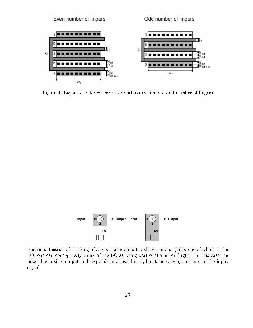
Figure 4: Layout of a MOS transistor with an even and a odd number of �ngers
Input Output
LO
Input Output
LO
Figure 5: Instead of thinking of a mixer as a circuit with two inputs (left), one of which is the
LO, one can conceptually think of the LO as being part of the mixer (right). In this case the
mixer has a single input and responds in a near-linear, but time-varying, manner to the input
signal.
26

Output
Input Output
LO
Fin
Input Signals
Output (mapped to positive frequencies)
Flo
Figure 6: The steady-state response of a linear periodically-varying system to a small complex
exponential stimulus. The large signals are represented with solid arrows and the small signals
with hollow arrows.
27
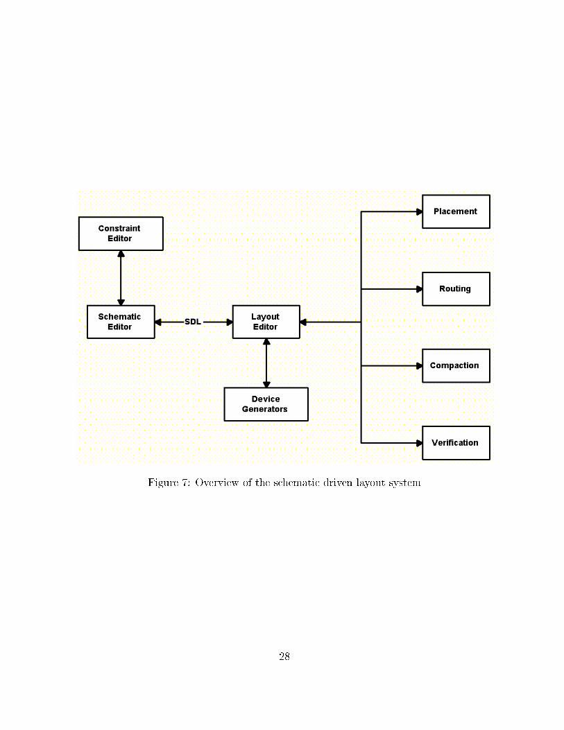
Figure 7: Overview of the schematic driven layout system
28

Figure 8: Cascode MOS transistor pair.
29

Figure 9: Overview of the template driven layout system
30

Figure 10: 4 Instances of a Di�erential Ampli�er, automatically generated based on a layout
template.
31

Figure 11: 2.4GHz DSS PA Gain Compression
32

Figure 12: 2.4GHz DSS PA Frequency Responce
33


