Page 1
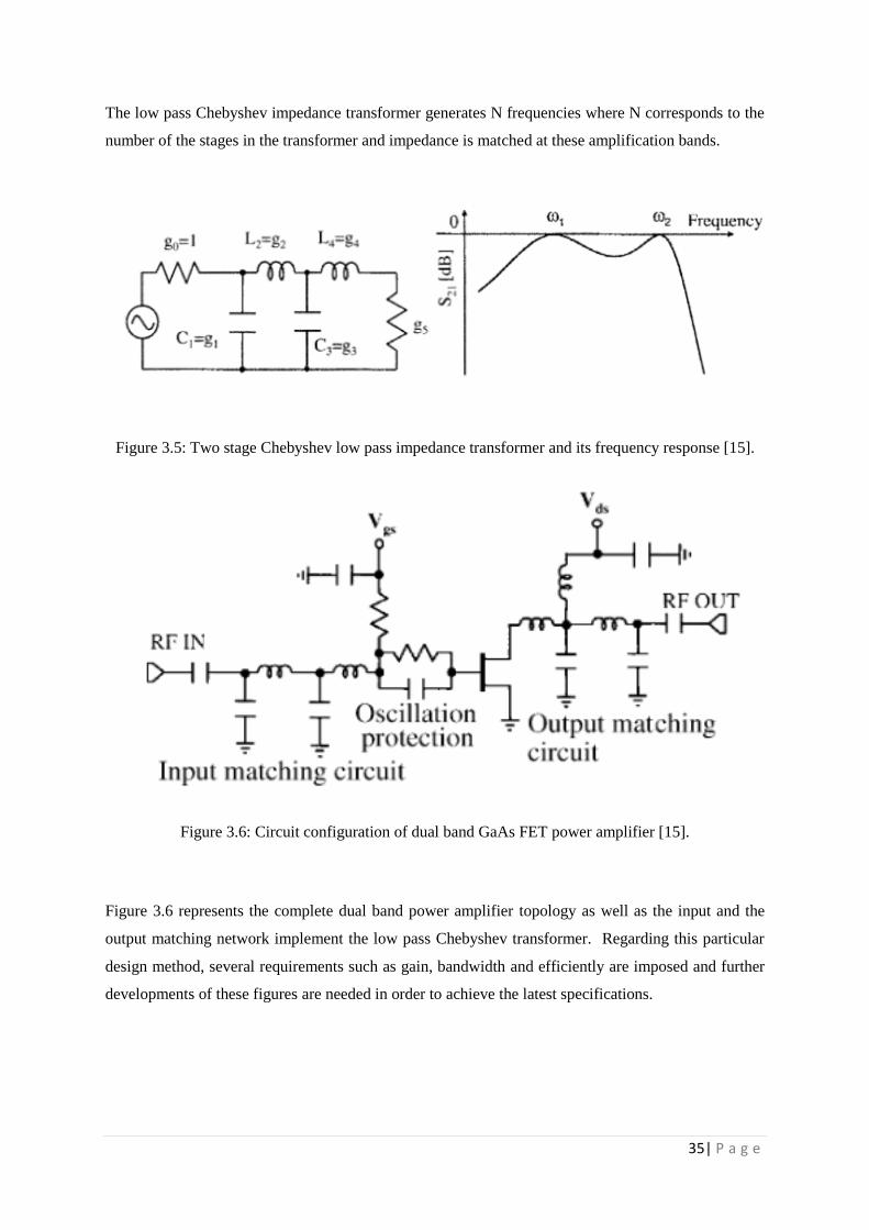
Design of a Dual Band Power Amplifier using Composite Right and Left
Handed Transmission Lines
A Thesis submitted to the University of Liverpool for the degree of
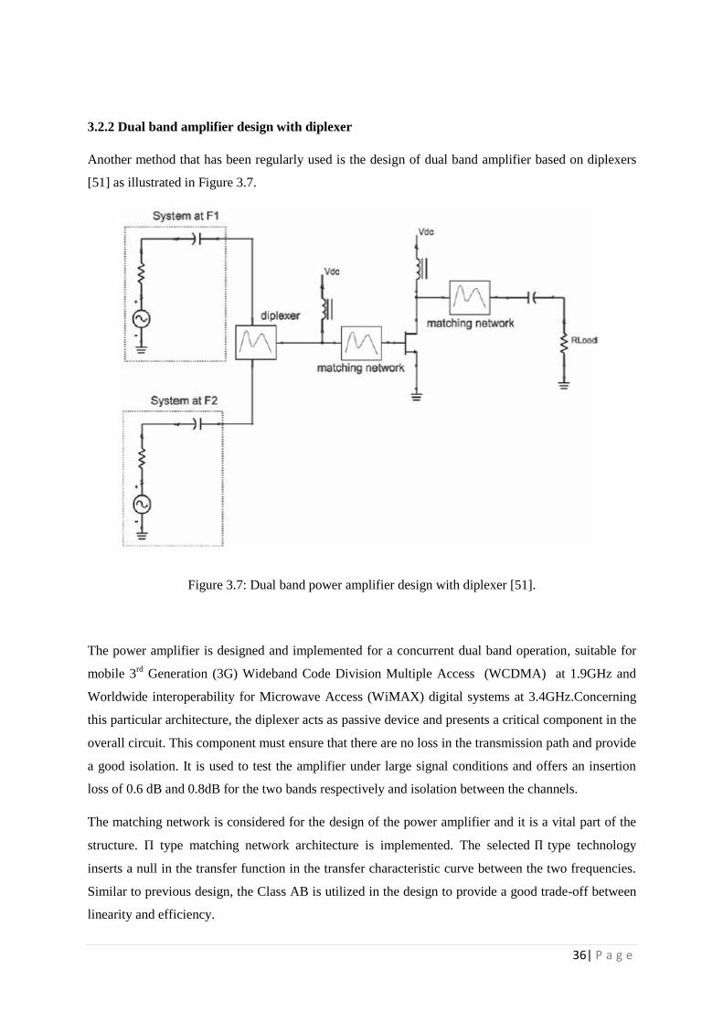
Master of Philosophy
By
Evangelos Kalantzis
Department of Electrical Engineering and Electronics
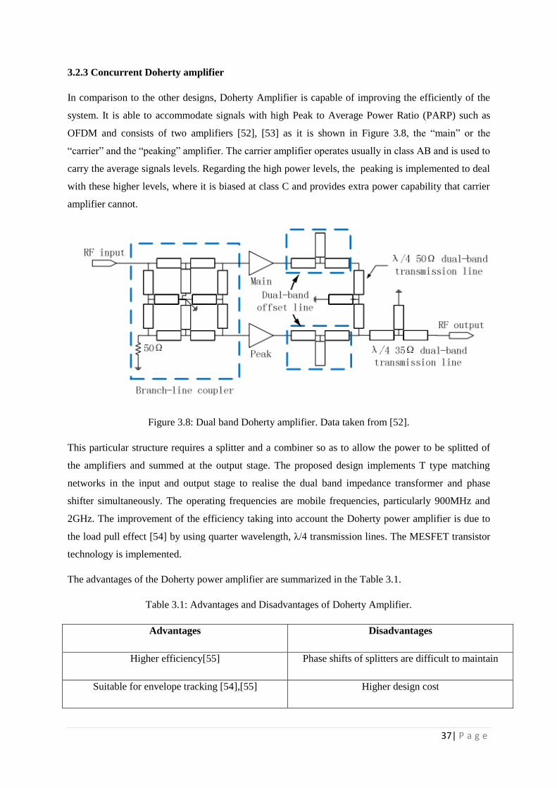
October 2016
Page 2
i| P a g e
Abstract
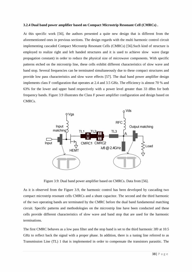
In wireless communications systems, multiple standards are used to meet demands of different
applications. This proliferation of wireless standards, operating over multiple frequency bands, has
increased the demand for radio frequency (RF) circuits and consequently Power Amplifiers (PAs) to
operate over multiple frequency bands with complex signals.
The PA is a major component of a transmitter as it is responsible for most of the total power
consumption in wireless communications equipment such as base stations and portable devices.
Except the power consumption, the design of PA systems for multi band and broadband operation
must consider high peak-to-average power ratio signals and the mismatch effect caused by the various
operating conditions. Hence the design of PA circuits that enhance total system efficiency and
reliability is a challenging task.
This work presents the design of a dual band Class E PA operating at 450 MHz and 700 MHz. The
proposed topology is based on the use of Composite Right Left Handed (CRLH) unit cells and
transmission lines. A CRLH unit cell exhibits a dual band frequency response because of its phase
characteristics. A PA circuit utilizing enhancement mode pseudomorphic (HEMT) transistor is
simulated in Agilent Advanced Design System (ADS) software and fabricated. A maximum Power
Added Efficiency (PAE) of 62% and 64% is achieved for an output power level of 39.7 dBm and 35.5
dBm at 450 MHz and 700MHz respectively. The presented approach can be applied to the design of
dual band matching networks for microwave circuits at two frequencies.
Page 3
ii| P a g e
Contents
Abstract
Contents
List of Figures
List of Tables
Acknowledgement
1 Introduction…………………………………...…………………………………………………..1
1.1 Motivation and thesis focus……………………………………………………………….…...1
1.2 Challenges of power amplifiers………………………………………………………….…….2
1.3 Design challenges for multi band power amplifier……………………...………………..……4
1.4 Design trends on dual band power amplifiers …………………………………………………6
1.5 Aims and design objectives………………………………………………….…………………7
1.6 Thesis structure………………………………………………………………………...……….9
1.7 Summary………………………………………………………………………………………..9
2 Power amplifier design fundamentals…………………………………………………………..10
2.1 Impedance matching networks………………………………………………………………..10
2.1.1 Transmission lines networks………………………………………………………………..12
2.1.2 L-type network configuration and applications……………………………………………..14
2.1.3 Π and T type networks……………………………………………………………………...15
2.1.4 Composite Right Left Handed (CRLH) networks…………………………….…………….17
2.2 Power amplifiers fundamentals………………………………………………….……………18
2.2.1 Conduction angle classes of power amplifiers…………………………………..………….19
2.2.2 Switching mode power amplifiers……………………………………………….………….22
Page 4
iii| P a g e
2.3 Classes of transistors……………………………………………………………………….…25
2.4 Selection of transistor…………………………………………………….….………………..28
2.5 Summary……………………………………………………………………………..…..........28
3 Dual band designs…………………………………………….…………………………….....…30
3.1 Dual band matching networks…..……………………………………………...…………..…30
3.1.1 Dual band impedance matching using resonators……………….………………....…….…30
3.1.2 T- type dual band matching using coupled line……………….………………...…....….….31
3.1.3 Dual band matching circuit using Composite Right Left Handed (CRLH) cells……..….....32
3.2 Dual band power amplifiers……..……………………………………………....….………...34
3.2.1 Dual band power amplifier based on two frequency matching…………………….…….....34
3.2.2 Dual band amplifier design with diplexer…………………………………………………..36
3.2.3 Concurrent Doherty amplifierr………...……………………………………………………37
3.2.4 Dual band power amplifier based on Compact Microstrip Resonant Cell CMRCs ……..…38
3.2.5 Dual band power amplifier using CRLH matching networks………………………............39
3.2.6 Comparison between power amplifier designs ………………………………….………….41
3.3 Summary…………………………………………………………………………….……...…42
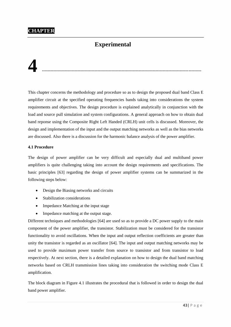
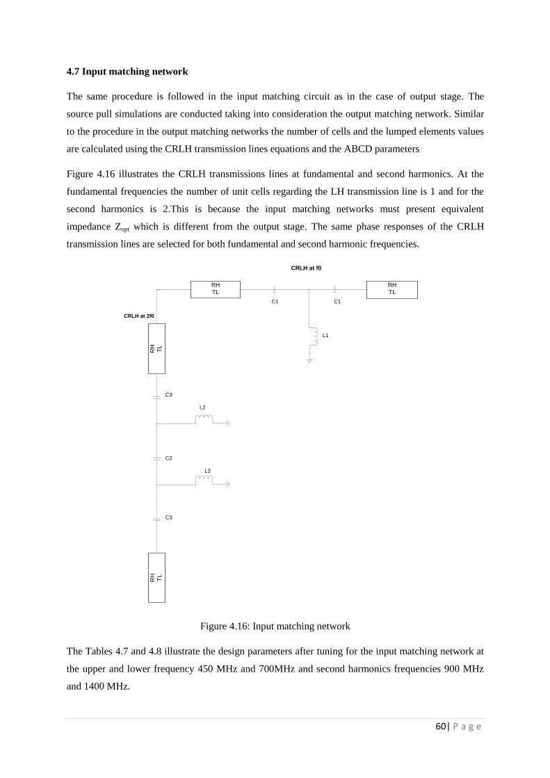
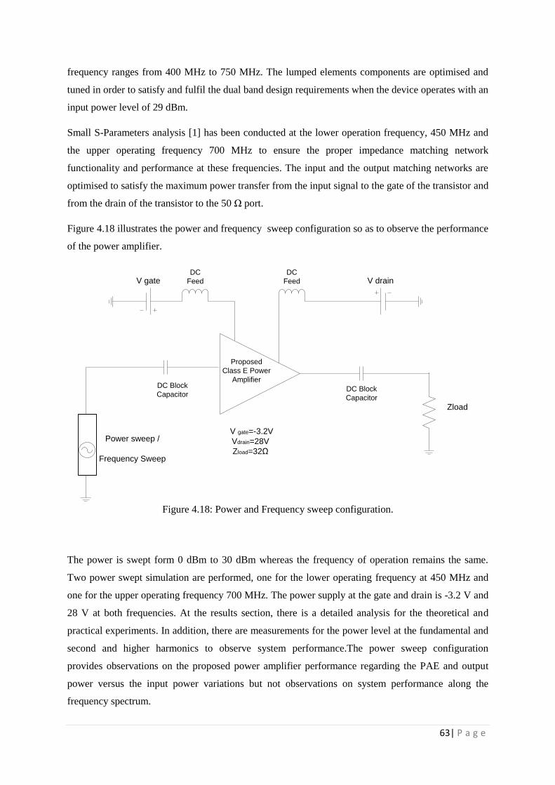
4 Experimental .…………………………………….……………………………....…………….43
4.1 Procedural…………………………………………………...……………….….…………….43
4.2 Load pull and source pull simulations……………….……………………..………………....45
4.3 General dual band response using Composite Right Left Handed (CRLH) Networks…….....49
4.4 Class E amplification architecture………………………………….…………………………52
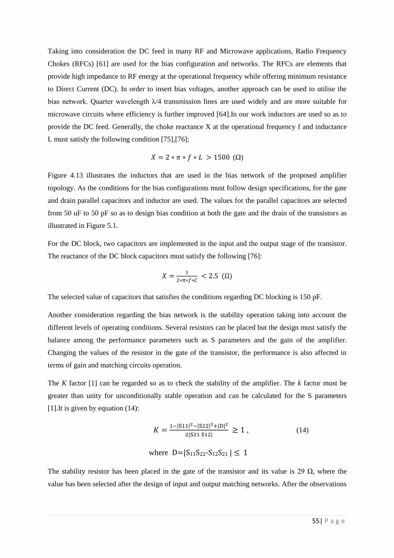
4.5 Bias network………………………………………………………………….……………….54
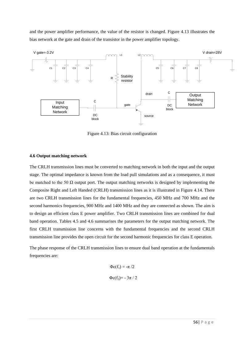
4.6 Output matching network…………………………………………………….…………...…..56
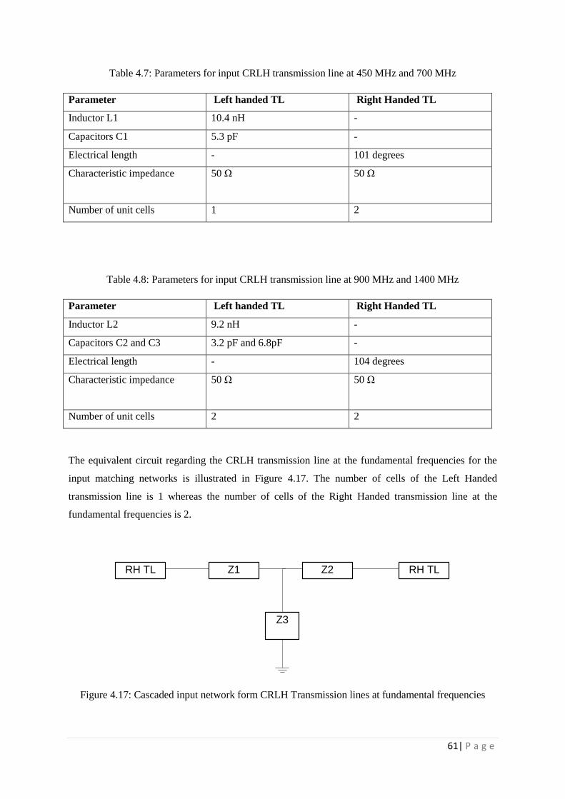
4.7 Input matching network……………………………………………………….…………....…60
4.8 Harmonic balance simulations…………………………………………….……….………....62
4.9 Summary………………………………………………..…………….……………………….64
Page 5
iv| P a g e
5 Fabrication…………………………………………..……………………….……….………...…..65
5.1 Fabrication procedure…………………..…………………………………………….…….…….65
5.1.1 HEMT transistor layout………………….…….……………………………………..………....66
5.1.2 Surface Mount Devices (SMDs)……….…………..…………………………….….…………..67
5.1.3 Overall structure………………………………………..……………….……….………………69
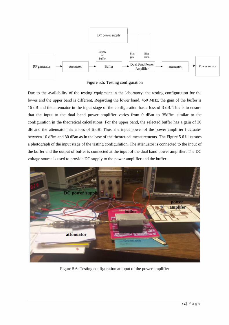
5.2 Experimental set up………………………………………………………………………………..71
5.3 Summary………………………………………………………..……….……….….….…..……..73
6 Results and Discussion……………………...…………………….…..……………….…..…..…..74
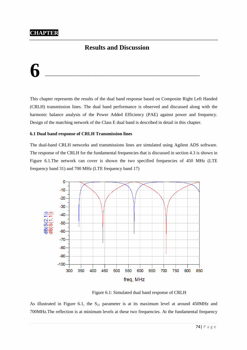
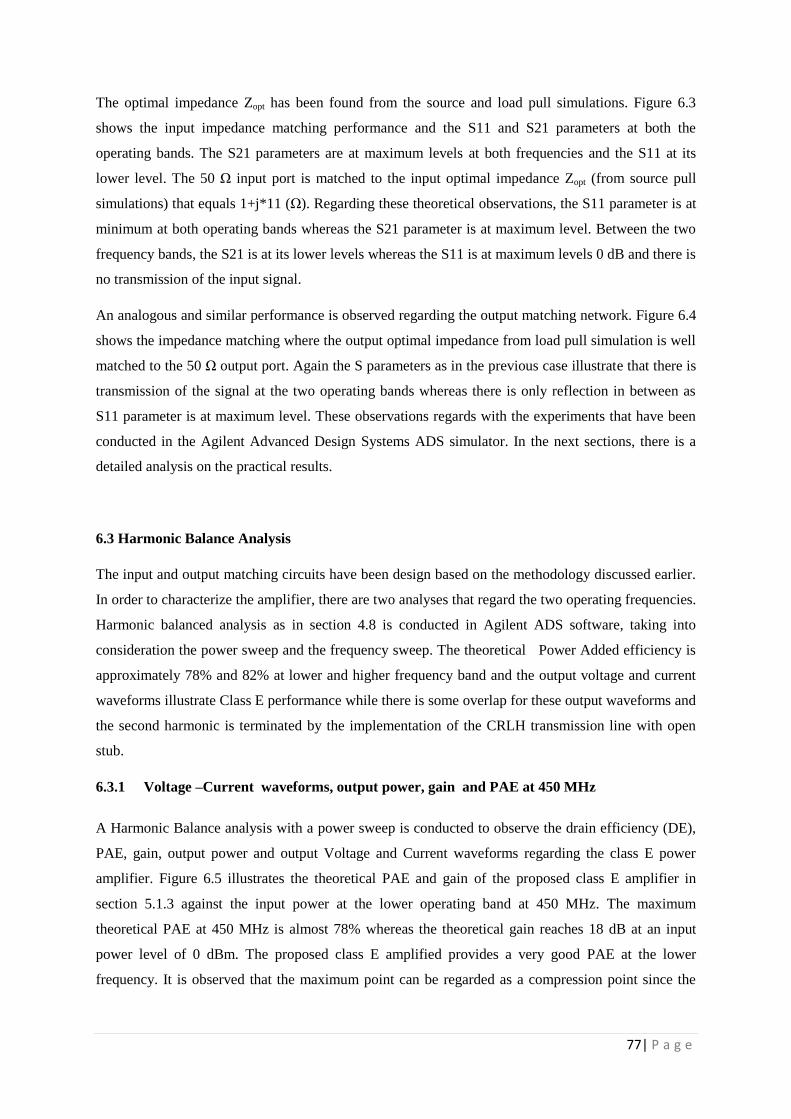
6.1 Simulated dual band response of CRLH ………….……….……….………………...…………...74
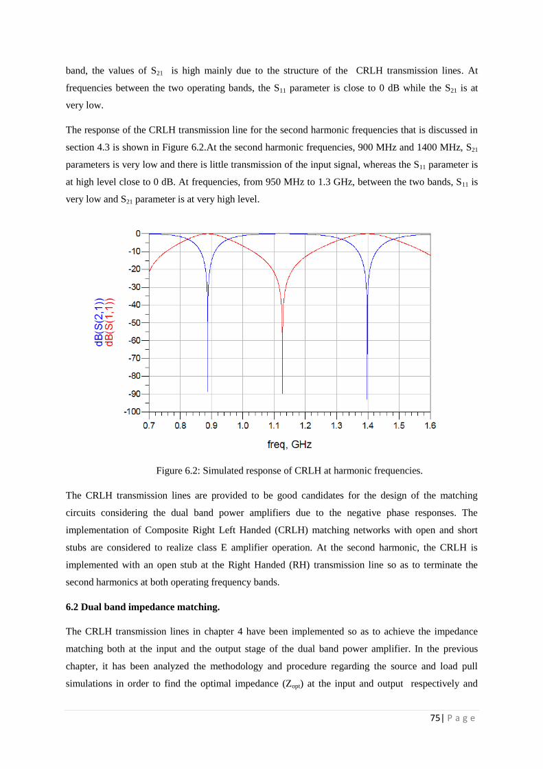
6.2 Simulated response of CRLH at harmonic frequencies ………………………....…….………….75
6.3 Harmonic balance analysis………………………………………………………………...……....76
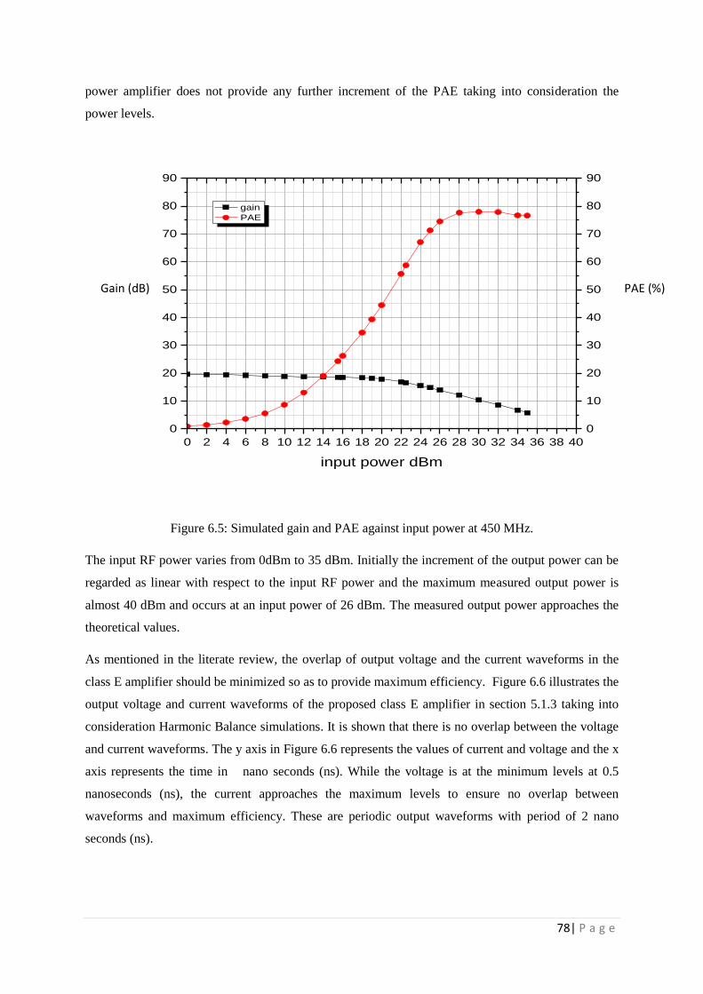
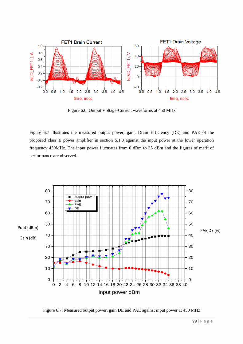
6.3.1 Voltage -Current waveforms, output power, gain and PAE at 450 MHz………….…................77
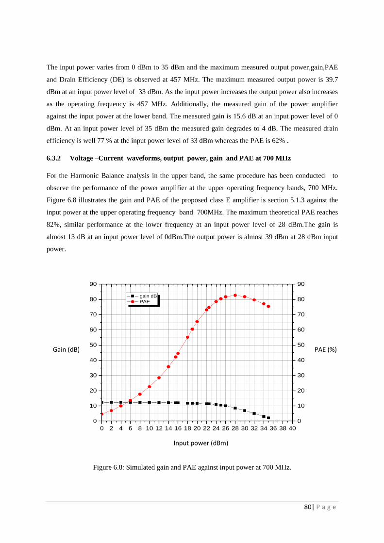
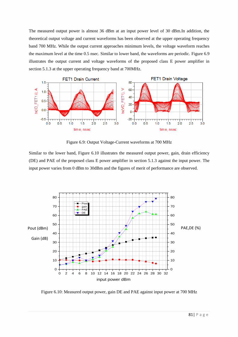
6.3.2 Voltage-Current waveforms, output power, gain and PAE at 700 MHz……………......………80
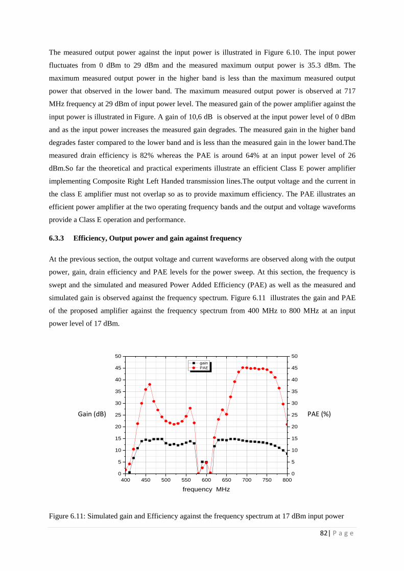
6.3.3 Efficiency, Output power and Gain against frequency…………………………....…...………..82
6.4 Discussion……………………………………………………………………….…..…….............84
7 Discussion and Future work………...………………………………………………...….…..…...87
References…………………………………………………………………………..….….………….91
Appendices…………………………………………………………………………..………………..98
Page 6
v| P a g e
List of Figures
1.1 Average power consumption in base stations. Data taken from [4] and [5]…………………….….2
1.2 Waveform with high peak to average power ratio. Data taken from [4]……………..……..….…..3
1.3 Evolution of peak to average power ratio for mobile communications. Data from [6].….…....…...4
1.4 Power amplifier drain efficiency [16]…………………………………………………………..…..5
1.5 Amplifiers with multiple switches. Data from [15]………………………………………………...6
1.6 Wideband amplifier. Data from [15]………………………………………………………….….....6
1.7 Simplified power amplifier Topology.Data from [18] ……………………………………………..7
2.1 Definition of bandwidth. Data from [24]…………………………………………………….…... 11
2.2 Multistage power amplifier. Data from [29]……………………………………………....………12
2.3 Transmission Line circuit model. Data from [31]…………………………………………………13
2.4 Impedance matching using transmission line [32]………………………………………………...14
2.5 Low-pass L network configuration. Data from [37]………………………………………………15
2.6 High-pass L network configuration. Data from [37]……………………………………………...15
2.7 Π network configuration. Data from [33]………………………………………………………...16
2.8 T network configuration. Data from [33]…………………………………………………………16
2.9: a) RH transmission line b) LH transmission line c) T shape CRLH unit cell [14]……………….17
2.10 Block of PA in transmitter architecture [37]…………………………………………………….18
2.11 Class A power amplifier configuration. Data from [37]…………………………………………19
2.12 I-V characteristics [37]…………………………………………………………………………..20
2.13 Class B power amplifier configuration. Data from [37]…………………………………………20
2.14 Efficiency against conduction angle. Data taken from [37]……………………………………...21
2.15 I-V waveforms [16]………………………………………………………………………………22
2.16 General class D architecture [38]………………………………………………………....……...23
2.17 Class E Amplifier output stage [37]……………………………………………………………...24
2.18 Class E Voltage –Current waveforms [39]………………………………………………………24
2.19 Class F power amplifier. Data taken from [13]………………………………………………….25
2.20 Classes of transistors. Data come from [4]……………………………………………………...26
Page 7
vi| P a g e
2.21 Transistor symbol. Data from [67]………………………………………………………...……..29
3.1 Dual band impedance matching networks using resonators. Data from [41]…………………….31
3.2 Dual band impedance matching networks using resonators. Data from [45] …………………….32
3.3 Π shape impedance matching networks using CRLH unit cells. Data from [18]…………………32
3.4 T shaped lumped element CRLH unit cell. Data from [58]……………………………………….33
3.5 Two stage Chebyshev low pass impedance transformer and its frequency response [15]………35
3.6 Circuit Configuration of dual band GaAs FET power amplifier [15]……………………………..35
3.7 Power Amplifier design with diplexer [51]……………………………………………………….36
3.8 Dual band Doherty Amplifier [52]……………………………………………….………………..37
3.9: Dual band power amplifier based on CMRCs. Data from [56]……………………………….….38
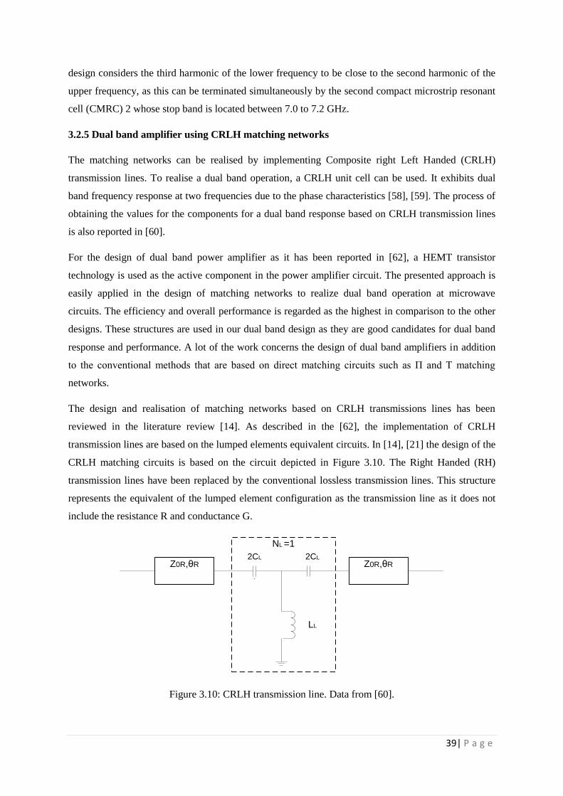
3.10 CRLH transmission line. Data from [60]………………………………………………………..39
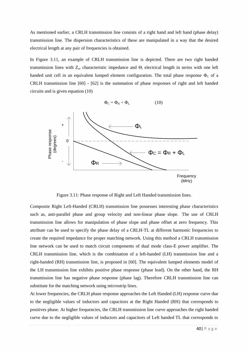
3.11 Phase response of Right and Left Handed transmission line [60]……………………………….39
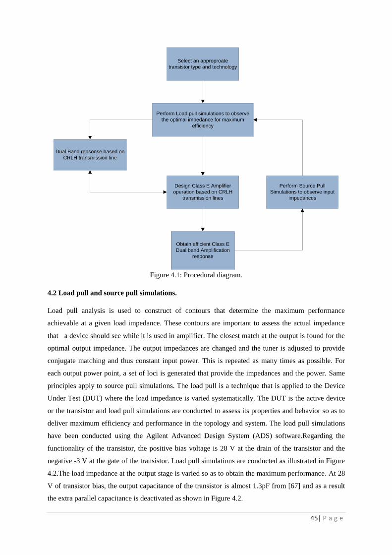
4.1 Procedural diagram………………………………………………………………………………..45
4.2 Transistor symbol. Data from [67]………………………………………………………………..46
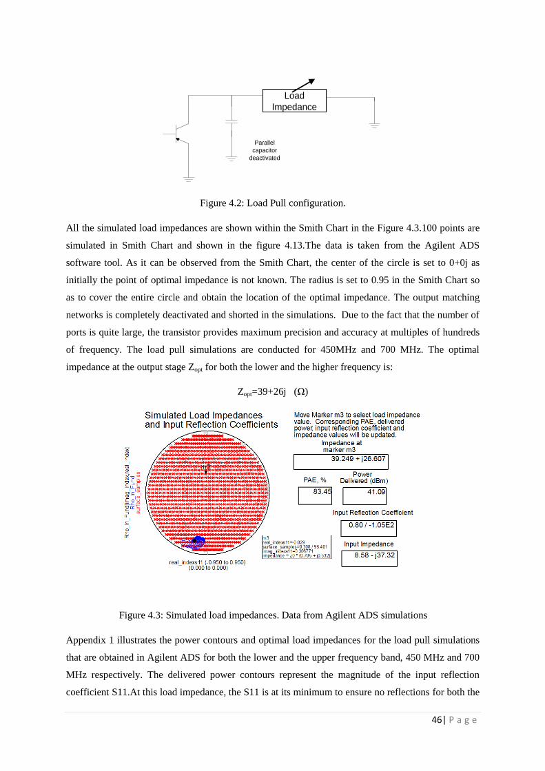
4.3 Load Pull configuration…………………………………………………………………………...46
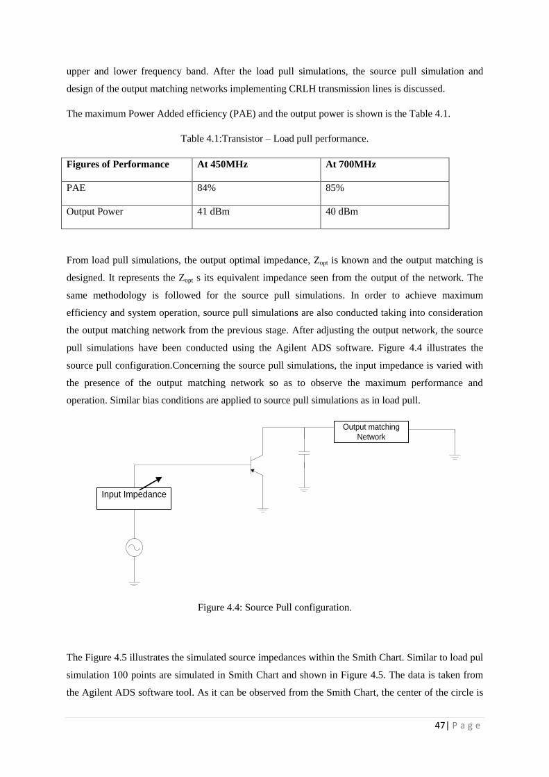
4.4 Source Pull configuration…………………………………………………………………………47
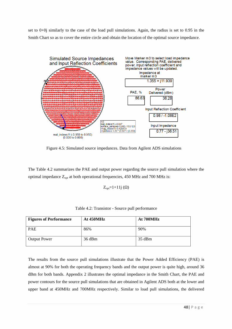
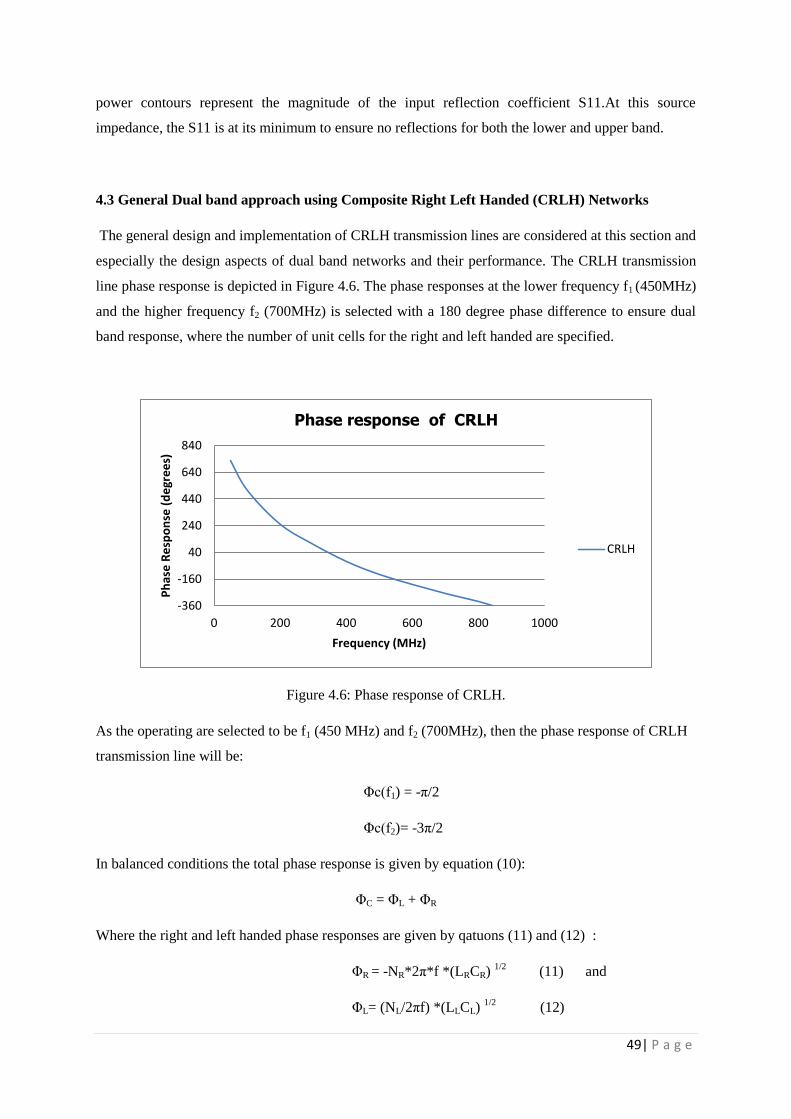
4.5 Phase response of CRLH. Data from [60]…………………………………………..…………….48
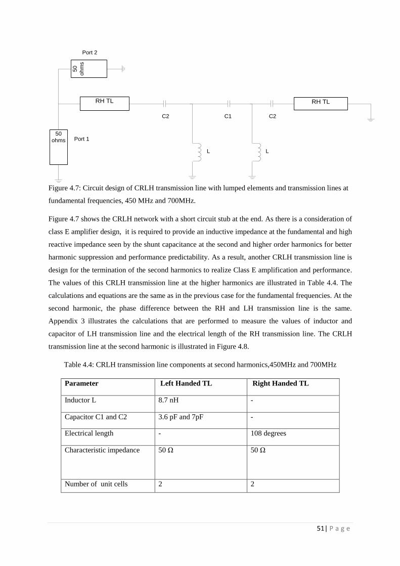
4.6 Circuit design of CRLH transmission line with lumped elements and transmissions lines at
fundamental frequencies [60] ………………………………………………………………………....50
4.7 Circuit design of CRLH transmission line with lumped elements and TLs at second harmonic
frequencies [60]………………………………………………………………………………………..51
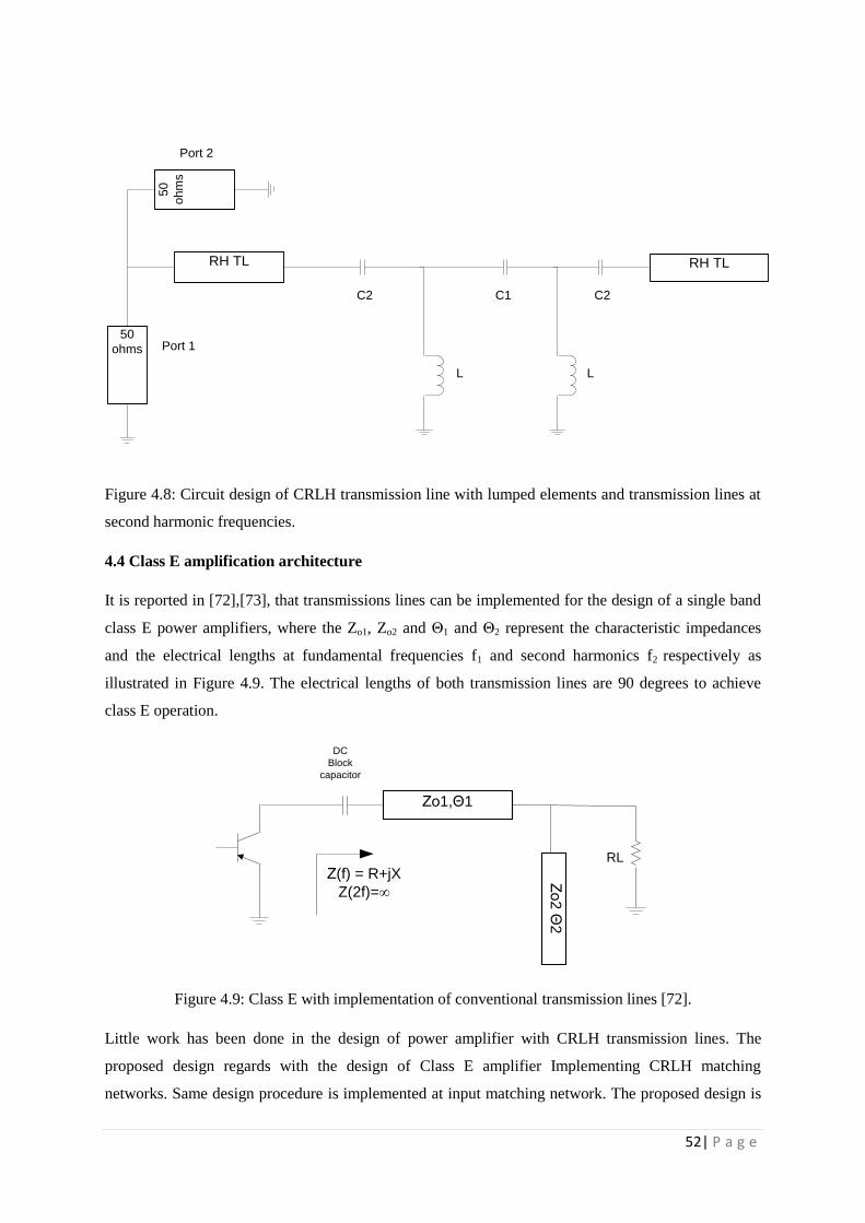
4.8 Class E with implementation of conventional Transmission lines [72]…………………………...52
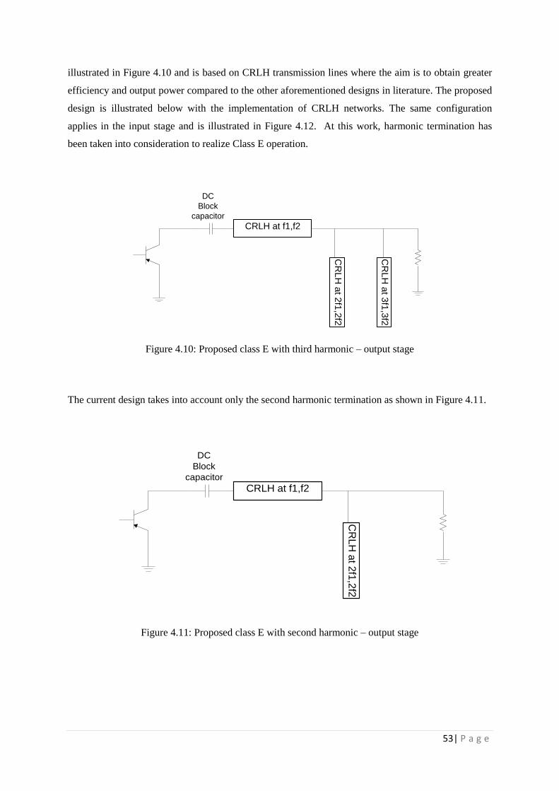
4.9 Proposed class E with third harmonic – output stage……………………………………………..52
4.10 Proposed class E with second harmonic – output stage……………………………………….…53
4.11 Proposed class E with second harmonic – input stage…………………………………………...53
4.12 Bias circuit configuration………..……………………………………………………………….54
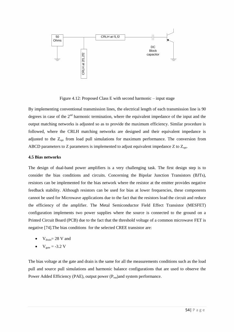
4.13 Output matching network…………..……………………………………………………….…....56
4.14 Cascaded output network form CRLH Transmission lines at fundamental frequencies………...57
Page 8
vii| P a g e
4.15 Input matching network…..……………………………………………………………….……..58
4.16 Cascaded input network form CRLH Transmission lines at fundamental frequencies……..…...60
4.17 Cascaded input network form CRLH Transmission lines at second harmonic frequencies….....61
4.18 Power and frequency sweep configuration [78]……….…………………………………….….63
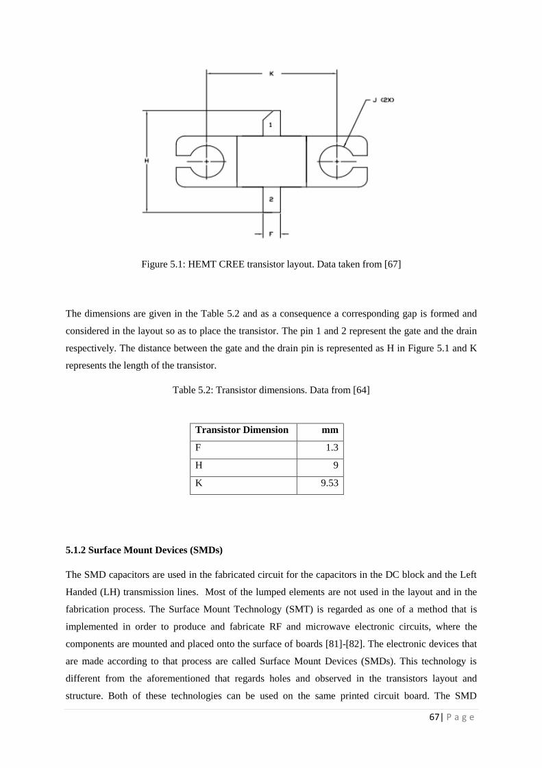
5.1 HEMT CREE transistor layout. Data taken from [67]……..……………………………………..67
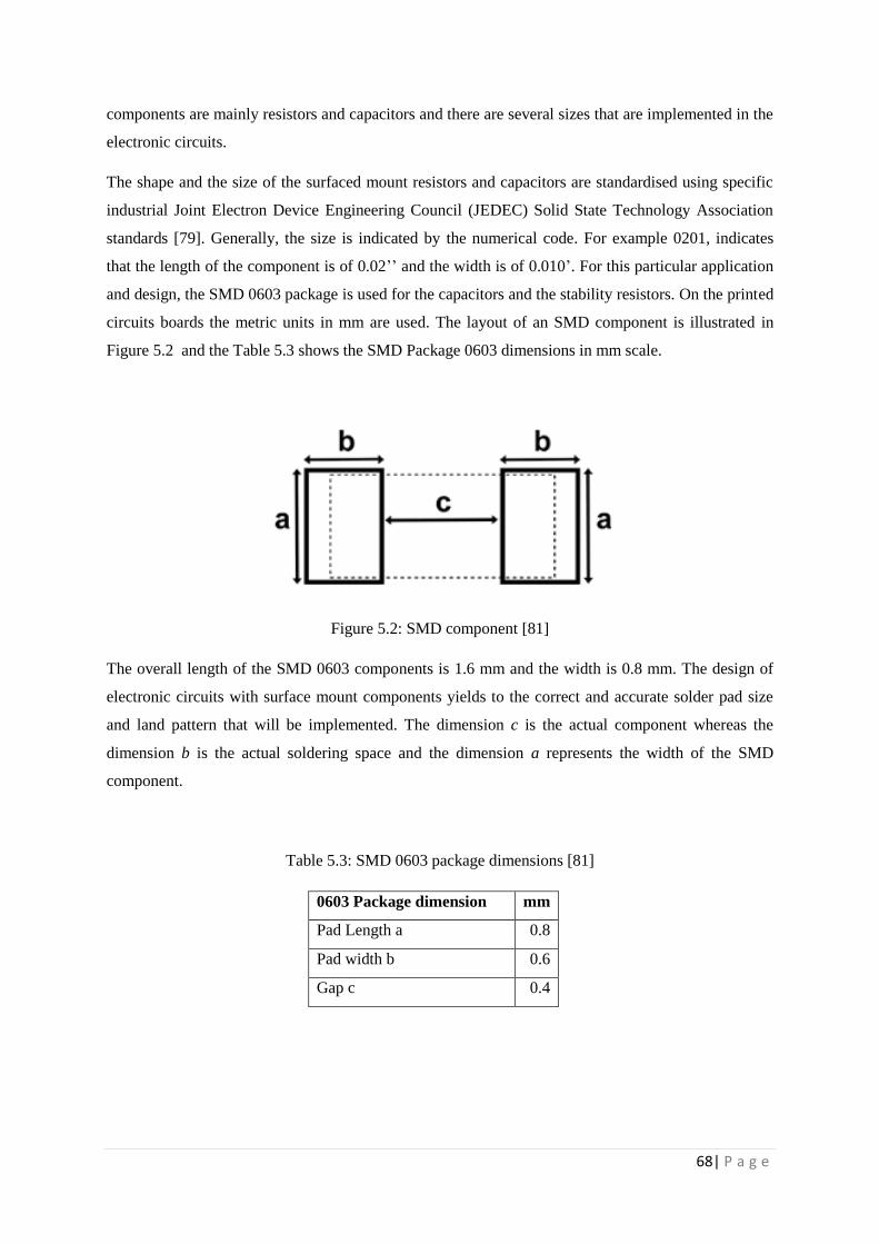
5.2 SMD component [81]…………………………………………………………………………..…68
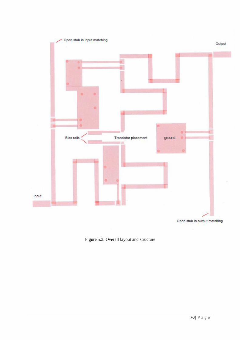
5.3 Overall layout and structure………………………………………………………………….…...70
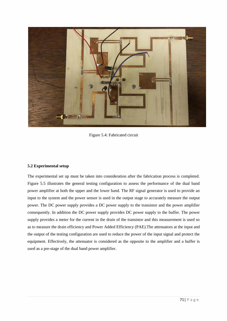
5.4 Fabricated circuit………………………………………………………………………………….71
5.5Testing configuration…………………………………………………………………….………...72
5.6 Testing configuration at input of the power amplifier……………………………………………72
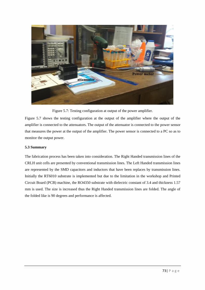
5.7 Testing configuration at the output of the power amplifier……………….……………………....73
6.1: Dual band response with short stub………………………………………………………………74
6.2 Dual band response with open stub…………………………………………………....…….….…75
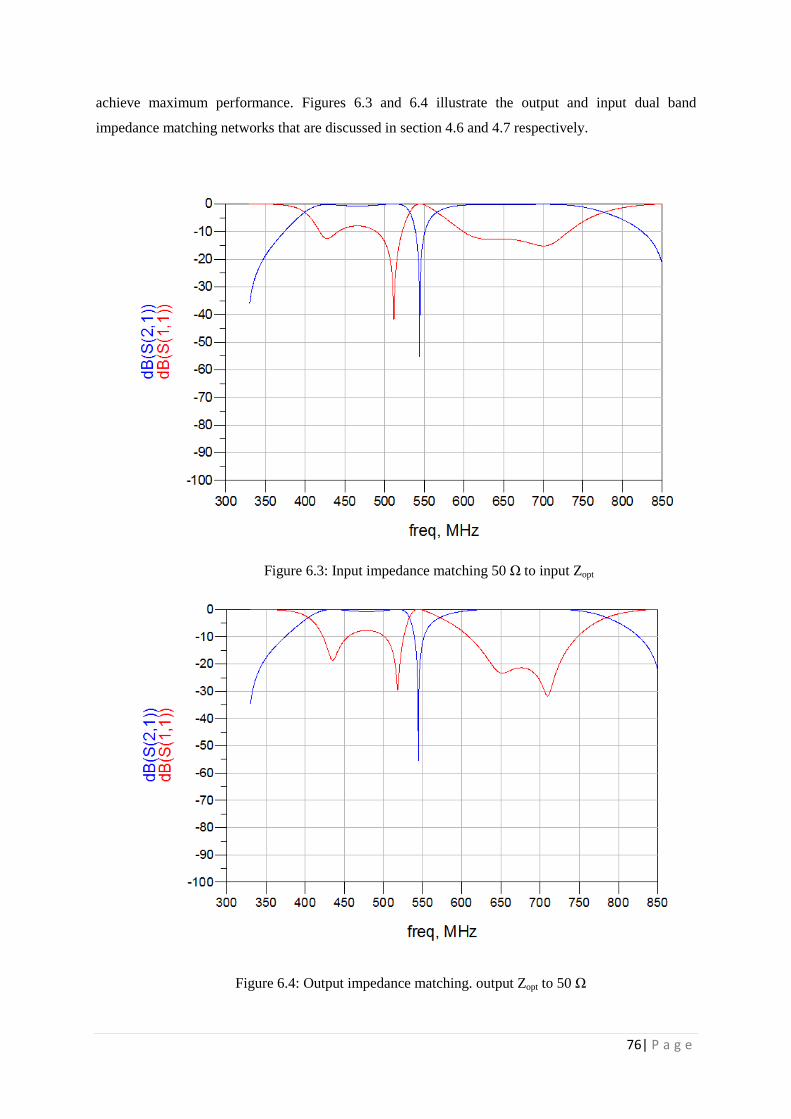
6.3 Input impedance matching 50 Ω to input Zopt………………………………………………….…77
6.4 Output impedance matching. Output Zopt to 50 Ω………………………………………………...76
6.5 Simulated gain and PAE against input power at 450 MHz.……………………………….………78
6.6 Output Voltage-Current waveforms at 450 MHz.....……………………………………………...79
6.7 Measured output power, gain,DE and PAE against input power at 450 MHz…...……..….……..79
6.8 Simulated gain and PAE against input power at 700 MHz ……………………………………….80
6.9 Output voltage-current waveforms at 700 MHz ………….…...…..………………....…………...81
6.10 Measured output power, gain, DE and PAE against input power at 700 MHz………………....81
6.11Simulated gain and Efficiency against the frequency spectrum at 17dBm input power……....…82
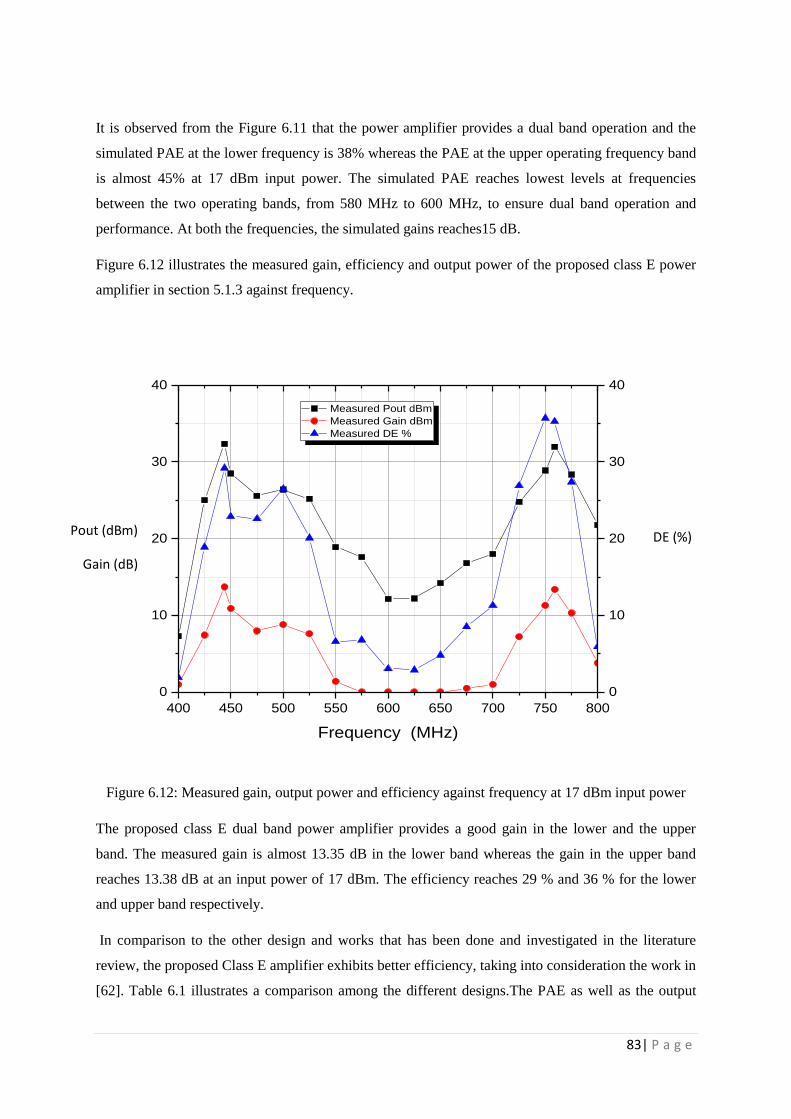
6.12 Measured gain, output power and efficiency against frequency at 17dBm input power .…...…..83
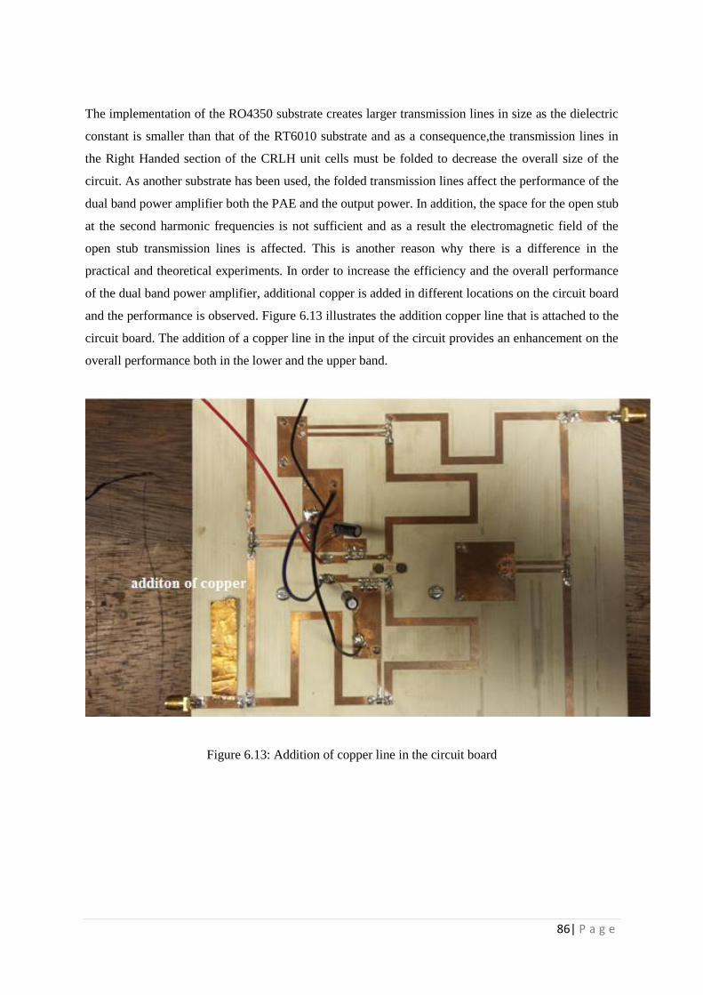
6.13 Addition of copper line in the circuit board……………………………………………………...86
Page 9
viii| P a g e
List of Τables
1.1 System requirements………………………………………………………………………..………8
2.1 FET and BJT comparison [40]………………………………………………………………….…27
2.2 CREE Transistor’s specifications[67]……………………...……………………………………...28
3.1 Advantages and Disadvantages of Doherty Amplifier…………………………………………....37
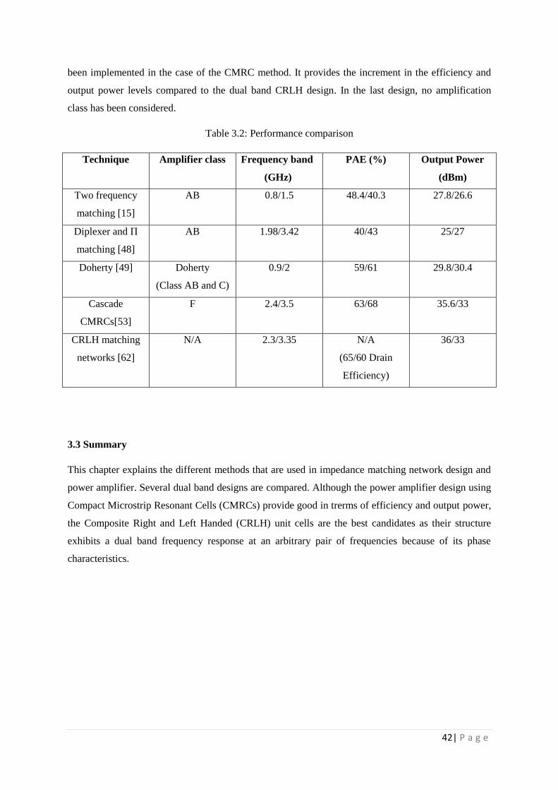
3.2 Performance comparison………………………………………………………………………..…42
4.1 Transistor – Load pull……………………………………………………………………………..47
4.2 Transistor - Source pull……………………………………………………………………………48
4.3 CRLH transmission line components at fundamental frequencies………………………………..50
4.4 CRLH transmission line components at second harmonics…………………………………….…51
4.5 Parameters for output CRLH transmission line at 450 MHz and 700 MHz……………………....56
4.6 Parameters for output CRLH transmission line at 900 MHz and 1400 MHz……………………..57
4.7: Parameters for input CRLH transmission line at 450 MHz and 700 MHz…………………….…61
4.8 Parameters for input CRLH transmission line at 900 MHz and 1400 MHz………………….…..61
5.5 Lumped element inductor to transmission line conversion…………………………………….…65
5.6 Transistor dimensions.Data from [64]….…………………………………………………………67
5.7 SMD 0603 package dimensions [81]……………………………………………………………...68
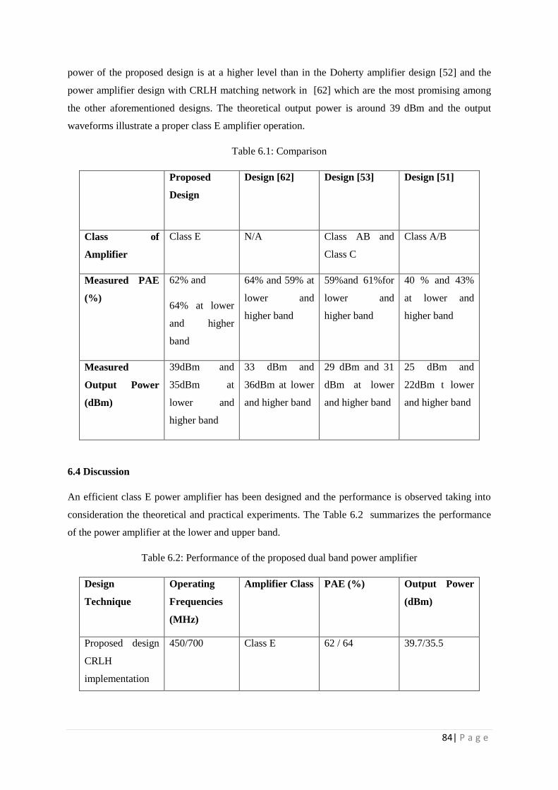
6.1 Comparison……………………………………………..……………………………….….……..84
6.2 Performance of the proposed dual band power amplifier……………………………….….……..84
Page 10
ix| P a g e
Notation
Δφ Phase shift of a single unit cell
η Drain efficiency
φ Phase shift
C Electrical capacitance
f1 Low operating frequency
f2 High operating frequency
G Gain
I Current
K Stability factor
N Number of unit cells
Pdc Dissipated power
Pin RF input power
Po RF output power
V Voltage
Y Admittance
Z Impedance
Page 11
x| P a g e
Abbreviations
BJT Bipolar-Junction Transistors
BS Base Station
BW Bandwidth
CRLH Composite Right/Left-Handed
DC Direct Current
DE Drain Efficiency
HEMT High Electron Mobility Transistor
FET Field Effect Transistor
GaN Gallium Nitride
HMSIW Half-Mode Substrate Integrated Waveguide
LH Left-Handed
MTM Metamaterial
OFDM Orthogonal Frequency Division Multiplexing
PA Power Amplifier
PAE Power Added Efficiency
PAPR Peak-to-Average Power Ratio
PCB Printed Circuit Board
RF Radio Frequency
RH Right-Handed
SMD Surface Mounted Device
TL Transmission Line
UE User Equipment
Page 12
xi| P a g e
Acknowledgement
First and foremost, I would like to sincerely thank my supervisors, Dr Jiafeng Zhou and Dr Ali Al
Ataby for giving me the opportunity to work with such an interesting research topic. I am more than
grateful taking into consideration their valuable guidance and feedback during the year. Thank you for
being always here to provide with suggestion and comments and mention ideas how to reach my
goals.
I am also grateful to Head of High Frequency Engineering Group and Deputy Head of Department of
Electrical Engineering and Electronics, Professor Yi Huang for allowing using the laboratory
equipment, his support and monthly meeting feedback and guidelines. He always inspires students
and improves individuals.
I would also like to thank my classmates, Abed Poursohab, Muaad Hussein, Moayad Kod and Yuan
Zhuang for creating a great working environment and their support and encouragement during the
experiments.
Page 13
1| P a g e
CHAPTER
Introduction
1 -----------------------------------------------------------------------------------------------------------------
This chapter concerns with the motivation, background on power amplifier, the challenges for multi
band Power Amplifier and the trends in the design implementations. In addition there is an
introduction to Composite Right Left Handed (CRLH) transmission lines as they are the matching
networks in proposed power amplifier design. The aim and design objectives are also considered in
this chapter.
1.1 Motivation and thesis focus
During the World War II in 1940s, the Radio Detection and ranging Radar system had been
developed and introduced as one of the major technological and defense applications regarding
communications engineering [1]. The term ‘Microwave signals’ refer to the alternative current signals
that covers the frequency band from 300 MHz up to 300 GHz, where the band is further divided to
several sub bands for different typical applications and uses. For instance, the K and Q bands cover
the range from 18 GHz to 26.5 GHz and 33 GHz to 50 GHz respectively and are used in applications
such as radar, satellite communications and radio astronomy. One of the advantages that the
microwave applications provide are the increased bandwidth and the use of line of the sight
propagation considering the tradeoff of complexity in the design of microwave electronic circuit. In
early 1950, John Bardeen and William Shockley invented the transistor devices that had posed a great
impact for the development and evolution of communications electronics and systems [1],[2]. The
transistor played a significant role in the design of critical electronics and microwave components
such as power amplifiers (PAs).Investigations have been conducted taking into account the transistor
evolution which has concluded into two main categories: the Bipolar Junction Transistors (BJTs) and
the Field Effect Transistor (FETs) [3]. The appropriate selection of transistor technology depends on
the design parameters and specification such as desired output power and frequency of operation. The
design of the active electronic components and circuits includes several challenges concerning the
development of efficient and innovative solutions for the communication systems. The design of
efficient power amplifiers for modern dual /multiband and broadband devices and latest
communications standards poses significant challenge for RF and microwave electronics.
Page 14
2| P a g e
The rapid development of wireless systems and standards require the need for dual band power
amplifiers [1] that can handle different standards and applications simultaneously with higher data
rates and bandwidths .In addition, enhanced features and services are available to mobile users.
Efficient and multiband devices are required to support the requirements and also 4rth generation
systems (4G) compatibility with legacy 2.5G and 3G standards.
In this context there is a need to investigate sophisticated solutions for the amplification stage of
modern transceivers. The thesis is focused on the design of dual band power amplifier for the Long
Term Evolution (LTE) mobile operating frequencies, 450 MHz and 700 MHz, to tackle the
aforementioned challenges in the modern communications systems. The performance and efficiency
of the power amplifier depend on the input and output matching networks. The dual band
performance is achieved by the utilization of Composite Right Left Handed (CRLH) transmission
lines. The CRLH transmission lines exhibit dual band response by frequency offset and phase slope
for matching network.
1.2 Challenges of power amplifiers
Power Amplifiers (PAs) are vital components and equipment for design of mobile base stations
(BSs) and user equipment (UE). According to [4] and [5], the amplification stage regarding the
operation of a base stations consumes about 65 % of the total power consumption whereas the air
conditioning, signal processing (time and frequency) and power supply consumes the rest of the
power. The power consumption in a base station circuit is illustrated in Figure 1.1. It is common place
the fact that PAs are crucial components taking into consideration the base station’s power
consumption, contributing to the total system efficiency [3]. Exactly the same happens in the
utilization of PA in the UE such as mobiles phones where the boost of the battery life is regarded as
the main issue of concern and development, thus increase the talk time limit of the phone.
Figure 1.1: Average power consumption in base stations. Data taken from [4] ,[5]
65%
15%
13%
7%
Power Consumption
Power Amplifier Air Condition Signal Processing Power Supply
Page 15
3| P a g e
In conjunction with the requirement regarding the system efficiency, the upcoming modulation
schemes and techniques pose significant constrains in the design and implementation of the
amplification stage. In comparison to the second generation 2G mobile systems, modem modulations
schemes such as Orthogonal Frequency Division Multiplexing (OFDM) and Spectral Efficient
Orthogonal Frequency Division Multiplexing (SEOFDM) [4] generate high data rates and bandwidth
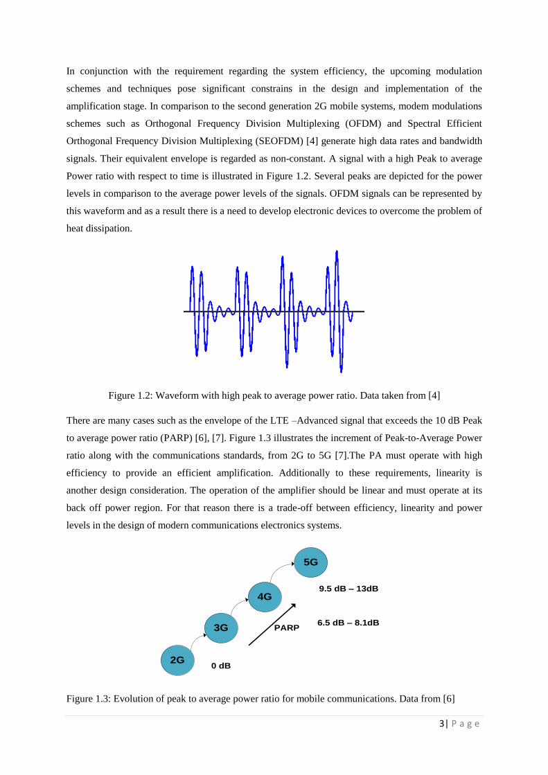
signals. Their equivalent envelope is regarded as non-constant. A signal with a high Peak to average
Power ratio with respect to time is illustrated in Figure 1.2. Several peaks are depicted for the power
levels in comparison to the average power levels of the signals. OFDM signals can be represented by
this waveform and as a result there is a need to develop electronic devices to overcome the problem of
heat dissipation.
Figure 1.2: Waveform with high peak to average power ratio. Data taken from [4]
There are many cases such as the envelope of the LTE –Advanced signal that exceeds the 10 dB Peak
to average power ratio (PARP) [6], [7]. Figure 1.3 illustrates the increment of Peak-to-Average Power
ratio along with the communications standards, from 2G to 5G [7].The PA must operate with high
efficiency to provide an efficient amplification. Additionally to these requirements, linearity is
another design consideration. The operation of the amplifier should be linear and must operate at its
back off power region. For that reason there is a trade-off between efficiency, linearity and power
levels in the design of modern communications electronics systems.
2G
4G
3G
5G
0 dB
9.5 dB – 13dB
PARP6.5 dB – 8.1dB
Figure 1.3: Evolution of peak to average power ratio for mobile communications. Data from [6]
Page 16
4| P a g e
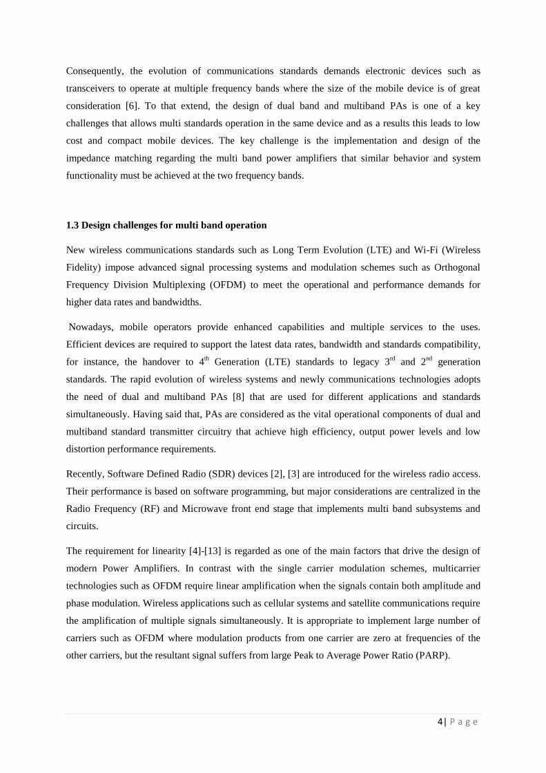
Consequently, the evolution of communications standards demands electronic devices such as
transceivers to operate at multiple frequency bands where the size of the mobile device is of great
consideration [6]. To that extend, the design of dual band and multiband PAs is one of a key
challenges that allows multi standards operation in the same device and as a results this leads to low
cost and compact mobile devices. The key challenge is the implementation and design of the
impedance matching regarding the multi band power amplifiers that similar behavior and system
functionality must be achieved at the two frequency bands.
1.3 Design challenges for multi band operation
New wireless communications standards such as Long Term Evolution (LTE) and Wi-Fi (Wireless
Fidelity) impose advanced signal processing systems and modulation schemes such as Orthogonal
Frequency Division Multiplexing (OFDM) to meet the operational and performance demands for
higher data rates and bandwidths.
Nowadays, mobile operators provide enhanced capabilities and multiple services to the uses.
Efficient devices are required to support the latest data rates, bandwidth and standards compatibility,
for instance, the handover to 4th Generation (LTE) standards to legacy 3
rd and 2
nd generation
standards. The rapid evolution of wireless systems and newly communications technologies adopts
the need of dual and multiband PAs [8] that are used for different applications and standards
simultaneously. Having said that, PAs are considered as the vital operational components of dual and
multiband standard transmitter circuitry that achieve high efficiency, output power levels and low
distortion performance requirements.
Recently, Software Defined Radio (SDR) devices [2], [3] are introduced for the wireless radio access.
Their performance is based on software programming, but major considerations are centralized in the
Radio Frequency (RF) and Microwave front end stage that implements multi band subsystems and
circuits.
The requirement for linearity [4]-[13] is regarded as one of the main factors that drive the design of
modern Power Amplifiers. In contrast with the single carrier modulation schemes, multicarrier
technologies such as OFDM require linear amplification when the signals contain both amplitude and
phase modulation. Wireless applications such as cellular systems and satellite communications require
the amplification of multiple signals simultaneously. It is appropriate to implement large number of
carriers such as OFDM where modulation products from one carrier are zero at frequencies of the
other carriers, but the resultant signal suffers from large Peak to Average Power Ratio (PARP).
Page 17
5| P a g e
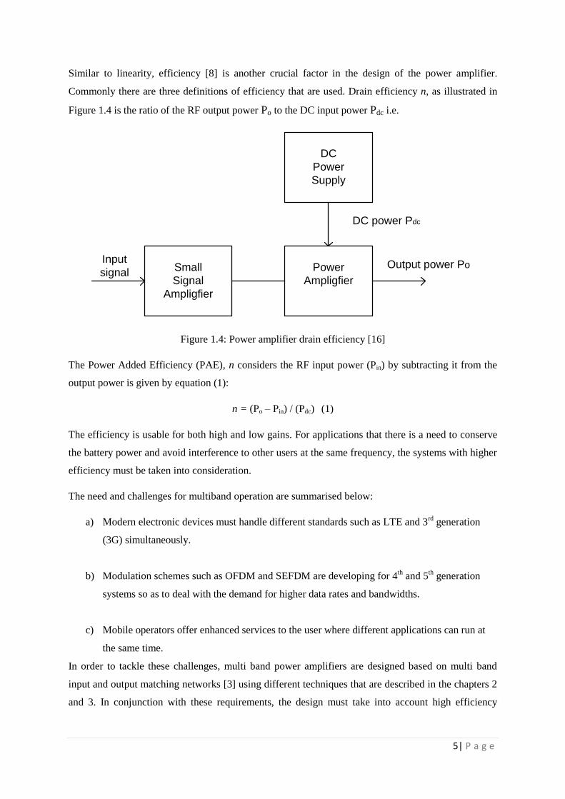
Similar to linearity, efficiency [8] is another crucial factor in the design of the power amplifier.
Commonly there are three definitions of efficiency that are used. Drain efficiency n, as illustrated in
Figure 1.4 is the ratio of the RF output power Po to the DC input power Pdc i.e.
Input
signalSmall
Signal
Ampligfier
Power
Ampligfier
Output power Po
DC
Power
Supply
DC power Pdc
Figure 1.4: Power amplifier drain efficiency [16]
The Power Added Efficiency (PAE), n considers the RF input power (Pin) by subtracting it from the
output power is given by equation (1):
n = (Po – Pin) / (Pdc) (1)
The efficiency is usable for both high and low gains. For applications that there is a need to conserve
the battery power and avoid interference to other users at the same frequency, the systems with higher
efficiency must be taken into consideration.
The need and challenges for multiband operation are summarised below:
a) Modern electronic devices must handle different standards such as LTE and 3rd
generation
(3G) simultaneously.
b) Modulation schemes such as OFDM and SEFDM are developing for 4th and 5
th generation
systems so as to deal with the demand for higher data rates and bandwidths.
c) Mobile operators offer enhanced services to the user where different applications can run at
the same time.
In order to tackle these challenges, multi band power amplifiers are designed based on multi band
input and output matching networks [3] using different techniques that are described in the chapters 2
and 3. In conjunction with these requirements, the design must take into account high efficiency
Page 18
6| P a g e
amplification in case of a longer battery lifetime and linearity to deal with the high PARP signals.
Moreover, the required output power, efficiency and distortion characteristics must be attained.
1.4 Design trends of dual band power amplifier.
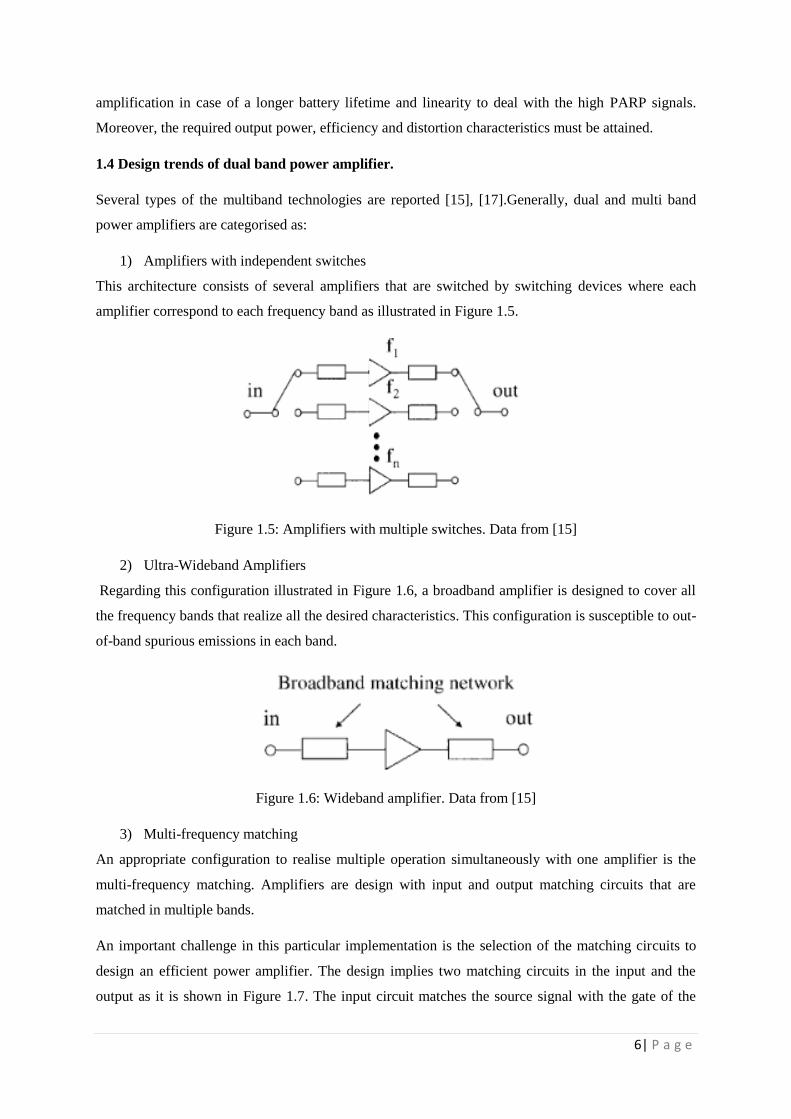
Several types of the multiband technologies are reported [15], [17].Generally, dual and multi band
power amplifiers are categorised as:
1) Amplifiers with independent switches
This architecture consists of several amplifiers that are switched by switching devices where each
amplifier correspond to each frequency band as illustrated in Figure 1.5.
Figure 1.5: Amplifiers with multiple switches. Data from [15]
2) Ultra-Wideband Amplifiers
Regarding this configuration illustrated in Figure 1.6, a broadband amplifier is designed to cover all
the frequency bands that realize all the desired characteristics. This configuration is susceptible to out-
of-band spurious emissions in each band.
Figure 1.6: Wideband amplifier. Data from [15]
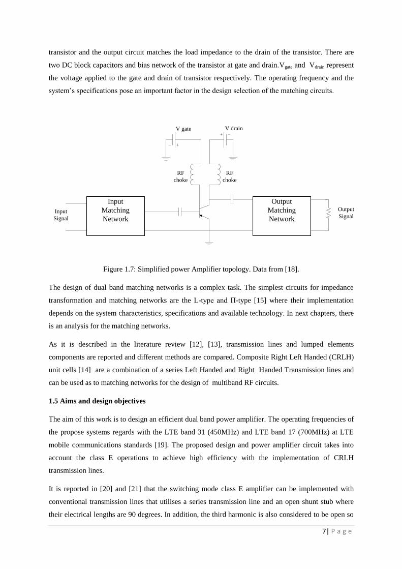
3) Multi-frequency matching
An appropriate configuration to realise multiple operation simultaneously with one amplifier is the
multi-frequency matching. Amplifiers are design with input and output matching circuits that are
matched in multiple bands.
An important challenge in this particular implementation is the selection of the matching circuits to
design an efficient power amplifier. The design implies two matching circuits in the input and the
output as it is shown in Figure 1.7. The input circuit matches the source signal with the gate of the
Page 19
7| P a g e
transistor and the output circuit matches the load impedance to the drain of the transistor. There are
two DC block capacitors and bias network of the transistor at gate and drain.Vgate and Vdrain represent
the voltage applied to the gate and drain of transistor respectively. The operating frequency and the
system’s specifications pose an important factor in the design selection of the matching circuits.
Input
Matching
Network
Output
Matching
Network
V gate V drain
Input
Signal
Output
Signal
RF
choke
RF
choke
Figure 1.7: Simplified power Amplifier topology. Data from [18].
The design of dual band matching networks is a complex task. The simplest circuits for impedance
transformation and matching networks are the L-type and Π-type [15] where their implementation
depends on the system characteristics, specifications and available technology. In next chapters, there
is an analysis for the matching networks.
As it is described in the literature review [12], [13], transmission lines and lumped elements
components are reported and different methods are compared. Composite Right Left Handed (CRLH)
unit cells [14] are a combination of a series Left Handed and Right Handed Transmission lines and
can be used as to matching networks for the design of multiband RF circuits.
1.5 Aims and design objectives
The aim of this work is to design an efficient dual band power amplifier. The operating frequencies of
the propose systems regards with the LTE band 31 (450MHz) and LTE band 17 (700MHz) at LTE
mobile communications standards [19]. The proposed design and power amplifier circuit takes into
account the class E operations to achieve high efficiency with the implementation of CRLH
transmission lines.
It is reported in [20] and [21] that the switching mode class E amplifier can be implemented with
conventional transmission lines that utilises a series transmission line and an open shunt stub where
their electrical lengths are 90 degrees. In addition, the third harmonic is also considered to be open so
Page 20
8| P a g e
that impedance at harmonic frequencies is infinity. These structures enable switching mode operation
but at single frequencies. In order to realise dual band operation and maximum performance, our
proposed design implements CRLH transmission lines not only for the fundamental frequencies but
also harmonic frequencies. The transistor technology is also taken into account in comparison to [22]
where only dual band amplification is reported without any real transistor device. Usually the output
power is not more than 2 W in most of the applications and literature. Our aim is to design an efficient
concurrent dual band class E amplifier with more than 3 W output power. Table 1.1 summarises the
proposed system requirements.
Table 1.1: System requirements
Class of Amplifier Switching mode, class E
Operational Frequencies LTE band 31 (450 MHz) ,
LTE band 17 (700MHz)
Efficiency >60% at the two frequency bands
Output Power >35 dBm
The objectives of the thesis are:
• Design dual band power amplifier at LTE band 31 (450MHz) and LTE band 17 (700MHz) at LTE
mobile communications standards
• Implement Composite Right Left Handed (CRLH) transmission lines so as to realize dual band
operation and performance
• Design matching networks and convert the (CRLH) transmission lines so as to obtain concurrent
dual band amplification
• Incorporate power amplifier design and techniques such as Switching mode amplification, load and
source pull simulations and techniques to obtain the maximum system efficiency are also considered.
• Implement the Agilent ADS software tool for simulations and theoretical results. Usage of Agilent
3D momentum
• Proceed with the fabrication process and PCB design to realize the amplifier circuit.
Page 21
9| P a g e
1.6 Thesis Structure
The Thesis is divided into the following chapters:
Chapter 2 concerns with the investigation and a background on matching networks and
power amplifier topologies for single band operation with their characterization. The design
objectives and contribution is also considered.
In Chapter 3, different techniques to design efficient dual band power amplifier is considered
for the several wireless standards and operating frequency bands.
Chapters 4 and 5 concern the experimental methodology and procedure along with a detailed
analysis regarding the relevant methodology and experimental setup. In conjunction the
implementation and the process of fabrication is discussed.
Chapter 6 regards with the analysis of the results from both the theoretical and practical
experiments along with a related discussion.
Chapter 7 regards with the conclusion and the proposed future work.
1.7 Summary
This work is concerned with the investigation of an efficient dual band power amplifier design for
cellular frequencies. Nowadays a lot of work is centralized in the design of modern electronic
components for the base stations. Many techniques are available for dual and multi band power
amplifiers and the purposes and scope of this work is to investigate efficient power amplifier based on
Composite Right Left Handed unit cells as input and output matching networks to provide dual band
responses and performance.
Page 22
10| P a g e
CHAPTER
Power amplifier design fundamentals
2 -----------------------------------------------------------------------------------------------------------------
This chapter represents the fundamentals of power amplifiers and matching networks and is divided
into three sections. The first section introduces the concept and importance of impedance matching
networks in general. In addition there is an introduction to Composite Right Left Handed (CRLH)
transmission lines as they are considered the matching networks in our proposed power amplifier
design .The second section concerns the power amplifier fundamentals and in the third section there is
a review on the different transistor classes and comparison between Field Effect Transistors (FETs)
and Bipolar Junction Transistors (BJTs). In addition there is a discussion for the selection of the
transistor for our proposed deign.
2.1 Impedance matching
Impedance matching network design is part of the power amplifier circuit subsystem at the input and
the output stage. In electronics and especially in the area of microwave engineering, impedance
matching regards the matching of the input impedance of an electrical load or the output impedance of
its signal source in order to maximize the power transfer or other parameters such as gain and
efficiency to the load. Generally, in the case of complex source impedance Zs and complex load
impedance ZL optimum matching [23] is achieved when equation (2) is satisfied:
Zs=ZL* (2)
Except the complex source and load matching, generally there are cases that the load or the source is
real terminations. For example there is a case where there is a matching from real termination to
complex or the opposite. The complex source impedance must be equal to the conjugate of the load
impedance for maximum power transfer [24].
Page 23
11| P a g e
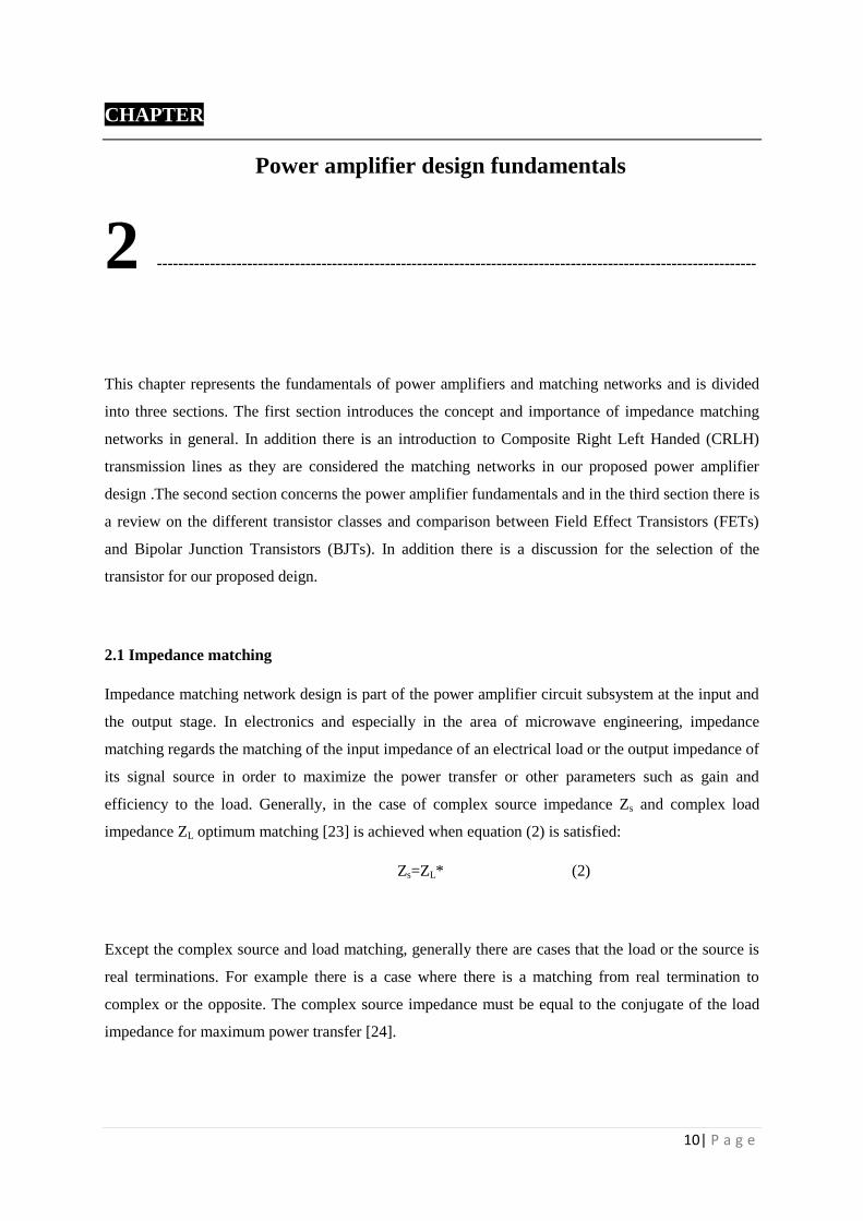
The bandwidth is defined as the 3 dB bandwidth that is the width between the lower and the higher
frequencies where the response of the systems is smaller by 3 dB than its response at the centre
frequency, f0 as shown in Figure 2.1.
Figure 2.1: Definition of bandwidth. Data from [24].
There are several types of electronics and electrical components that are implemented between the
source and the load in order to achieve impedance matching [25] - [27]. Some of the sophisticated
components that can be used for impedance matching are:
Transformers.
Transmission lines.
A combination of inductor and capacitors networks.
The design of the amplifier depends on the input and the output matching networks. The input
matching network is used to match the 50 Ω input source to the gate of the transistor. The output
matching network matches the drain of the transistor or the conjugate output impedance of the
transistor to the 50 Ω load in the output stage.
Matching networks are being used to transfer the maximum power from the input source to the input
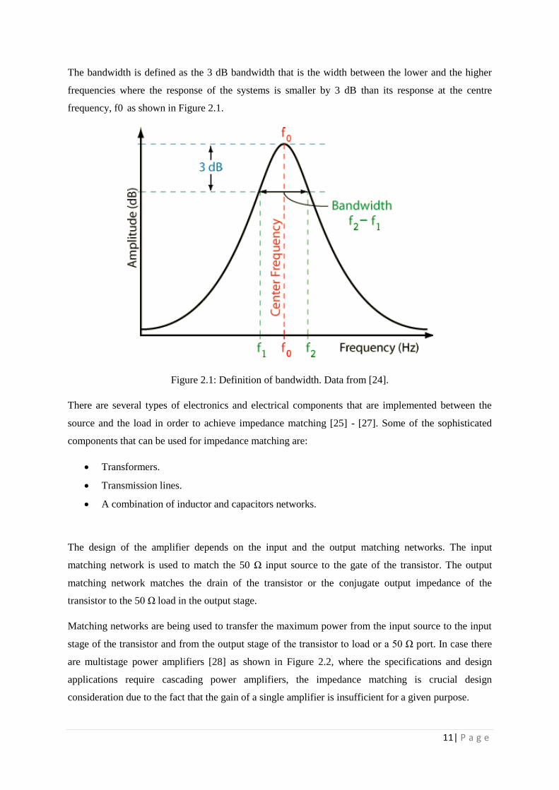
stage of the transistor and from the output stage of the transistor to load or a 50 Ω port. In case there
are multistage power amplifiers [28] as shown in Figure 2.2, where the specifications and design
applications require cascading power amplifiers, the impedance matching is crucial design
consideration due to the fact that the gain of a single amplifier is insufficient for a given purpose.
Page 24
12| P a g e
Amplifier A Amplifier B Amplifier C
Zout Zin Zout Zint
Input Output
Figure 2.2: Multistage power amplifier. Data from [29].
Amplifiers have the capability to increase the magnitude of the input signal. The term for an amplifier
output and input ratio is also known as gain as a ratio of equal units and as a result gain is unitless
measurement. The power gain (A) in dB, can be expressed by equation (3):
A= 10 * log(Po / Pin) (3)
Similar to power gain, there is the voltage and the current gain also in DC and AC. The gain in
multistage amplifier systems is the multiplication of the individual amplifier gains. Therefore the
impedance values in the input and output stage has an effect on gain in multi stage amplifiers as
there is always loss of signal amplitude due to the coupling of the cascaded power amplifier stages.
The overall gain is actually less than the product of the individual gains of each power amplifier. Due
to the coupling of multistage there is always a decrement of the amplitude of the signal. For that
reason, the design of impedance matching is of great importance.
2.1.1 Transmission line networks
Usually transmission lines are used so as to design impedance matching networks. For example, in the
case of a transmitter, the output stage is connected to the input of an antenna using a transmission line.
More often, the transmission line is a type of microstrip line. Depending on the application and design
specification, the transmission line can be a twisted pair or some other medium [30]. A connecting
cable can represent a transmission line when its length is greater than λ / 8 concerning the operating
frequencies where the relationship between wavelength λ and frequency is given by equation (4):
𝜆 = 𝑐
𝑓 (4)
where c is the speed of light and f is the operating frequency.
Page 25
13| P a g e
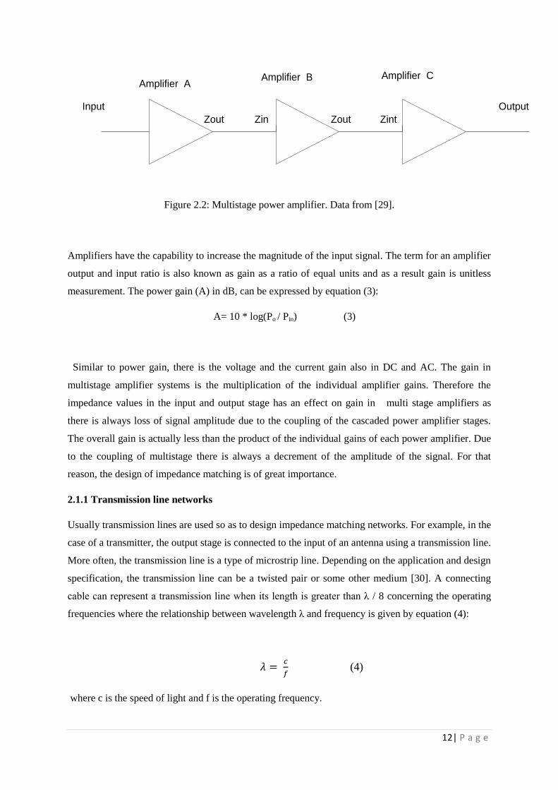
The equivalent circuit model [31] of a transmission line is illustrated in Figure 2.3. It contains the
impedance Z which is equal to 𝑍 = 𝑅 + 𝑗𝜔𝐿 and admittance Y which is equal to 𝑌 = 𝐺 + 𝑗𝜔𝐶. The
model represents the transmission line as a series of two port elements. Each represents a small
segment of the line.
R
L
GC
Figure 2.3: Transmission line circuit model. Data from [31].
The equivalent circuit of a transmission line consists of the following components:
Distributed resistance R of the conductors (expressed in Ω per unit length).
Inductance L due to the magnetic field around the wires (H per unit length).
Conductance G of the dielectric material (Siemens per unit length).
Capacitance C between the two conductors (Farads per unit length).
A lossless line is defined as a transmission line that has no resistance and dielectric loss. The
transmission lines have characteristic impedance Z0 [31] and for a lossless transmission line where
the R and G are zero, the characteristic impedance is given by equation (5):
𝑍0 = √𝐿
𝐶 (5)
There are special cases to match real source impedance to real load impedance as illustrated in Figure
2.4. This can be achieved using quarter wavelength (λ/4) transmission lines as it is illustrated in the
Figure 2.4, where its equivalent input impedance Zin is given by :
Zin= Z02 / ZL (6)
Page 26
14| P a g e
Z0
ZL
Zs
Source
Zin
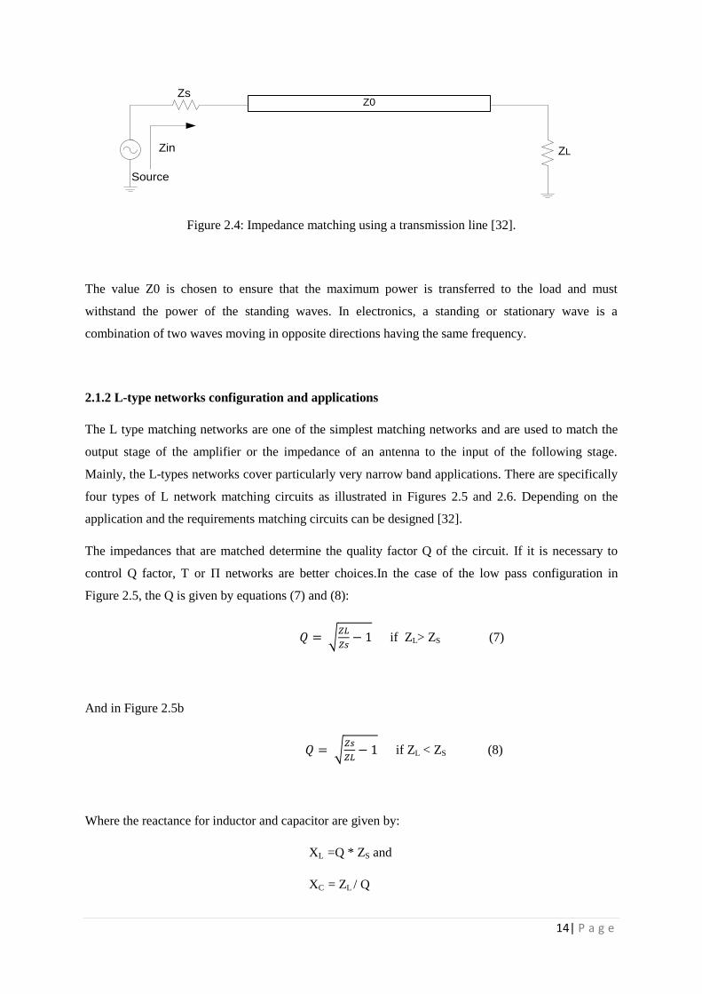
Figure 2.4: Impedance matching using a transmission line [32].
The value Z0 is chosen to ensure that the maximum power is transferred to the load and must
withstand the power of the standing waves. In electronics, a standing or stationary wave is a
combination of two waves moving in opposite directions having the same frequency.
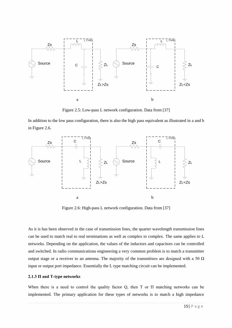
2.1.2 L-type networks configuration and applications
The L type matching networks are one of the simplest matching networks and are used to match the
output stage of the amplifier or the impedance of an antenna to the input of the following stage.
Mainly, the L-types networks cover particularly very narrow band applications. There are specifically
four types of L network matching circuits as illustrated in Figures 2.5 and 2.6. Depending on the
application and the requirements matching circuits can be designed [32].
The impedances that are matched determine the quality factor Q of the circuit. If it is necessary to
control Q factor, T or Π networks are better choices.In the case of the low pass configuration in
Figure 2.5, the Q is given by equations (7) and (8):
𝑄 = √𝑍𝐿
𝑍𝑠− 1 if ZL> ZS (7)
And in Figure 2.5b
𝑄 = √𝑍𝑠
𝑍𝐿− 1 if ZL < ZS (8)
Where the reactance for inductor and capacitor are given by:
XL =Q * ZS and
XC = ZL / Q
Page 27
15| P a g e
ZL
Zs
Source
L
C
L TYPE
ZL>Zs
ZL
Zs
Source
L
C
L TYPE
ZL<Zs
a b
Figure 2.5: Low-pass L network configuration. Data from [37]
In addition to the low pass configuration, there is also the high pass equivalent as illustrated in a and b
in Figure 2.6.
ZL
Zs
Source L
CL TYPE
ZL>Zs
ZL
Zs
Source L
CL TYPE
ZL<Zs
a b
Figure 2.6: High-pass L network configuration. Data from [37]
As it is has been observed in the case of transmission lines, the quarter wavelength transmission lines
can be used to match real to real terminations as well as complex to complex. The same applies to L
networks. Depending on the application, the values of the inductors and capacitors can be controlled
and switched. In radio communications engineering a very common problem is to match a transmitter
output stage or a receiver to an antenna. The majority of the transmitters are designed with a 50 Ω
input or output port impedance. Essentially the L type matching circuit can be implemented.
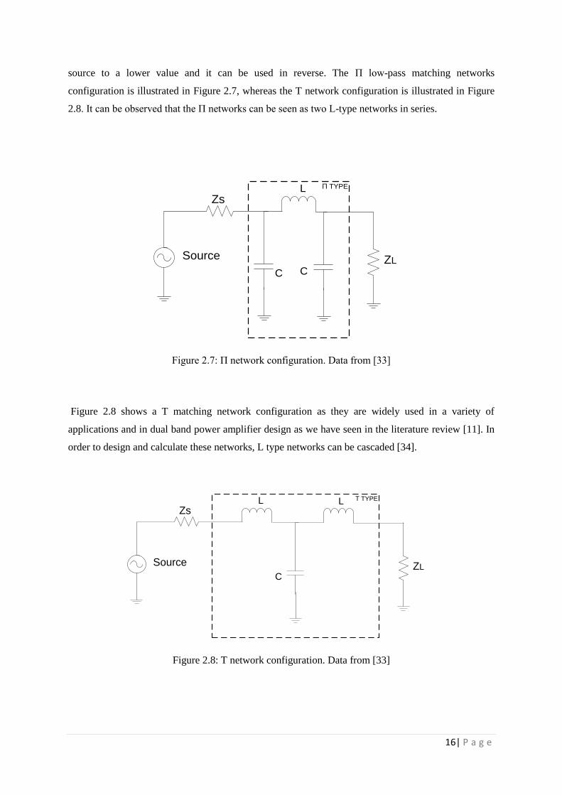
2.1.3 Π and T-type networks
When there is a need to control the quality factor Q, then T or Π matching networks can be
implemented. The primary application for these types of networks is to match a high impedance
Page 28
16| P a g e
source to a lower value and it can be used in reverse. The Π low-pass matching networks
configuration is illustrated in Figure 2.7, whereas the T network configuration is illustrated in Figure
2.8. It can be observed that the Π networks can be seen as two L-type networks in series.
ZL
Zs
Source
L
C
Π TYPE
C
Figure 2.7: Π network configuration. Data from [33]
Figure 2.8 shows a T matching network configuration as they are widely used in a variety of
applications and in dual band power amplifier design as we have seen in the literature review [11]. In
order to design and calculate these networks, L type networks can be cascaded [34].
ZL
Zs
Source
L
C
Τ TYPEL
Figure 2.8: T network configuration. Data from [33]
Page 29
17| P a g e
2.1.4 Composite Right Left Handed (CRLH) networks
Among the efforts for dual-band operation stands the implementation of PA circuits based on the
newly introduced concept of Metamaterial (MTM) structures [14]-[16]. The term MTM refers to
artificial effectively homogeneous electromagnetic structures with unusual properties that are not
readily available in nature [30]. The properties of the metamaterial transmission lines have found
successful application to the design of a plethora of devices, from antennas to microwave sensors
[20]. The proposed design and topology considered in later Chapter is a dual-band power amplifier
that is inspired from the MTM concept and based on Composite Right/Left-Handed (CRLH) TL unit
cells for both the input and output matching networks. MTM have become very interesting topic due
to their unusual properties and characteristics. A way to create a media with metamaterial
characteristics is to design circuits that model their properties. By implementing a repetition of unit
cells a particular class of metamaterials can be designed that consists of Right Handed and Left
Handed CRLH Transmission lines. These circuits incorporate lumped elements components such as
capacitors and inductors. In addition, they can include conventional transmission lines too. The design
of dual band matching networks in the power amplifier topology is a challenging task. In some cases,
the same amplification performance must be achieved at lower and higher frequencies simultaneously.
In contrast to conventional and common design methods that are discussed in chapter 2, CRLH unit
cells are implemented for matching networks in broadband and multiband microwave circuits. In
addition CRLH networks are found usefull in the design of couplers and diplexers [35]. The CRLH
transmission line is just a series combination of Left handed (LH) and Right handed (RH)
transmission lines [14].The circuit and the equivalent lumped element configuration of these LH and
RH transmission lines and a CRLH unit cell is illustrated in Figure 2.9. At these circuits, the
propagation constant and the characteristics impedance can be estimated similar to the case of
conventional transmission lines. Additional unit cells can be put in series depending on the application
and design specifications.
CR
LR CL
LL
LR CL
CRLL
a b c
Figure 2.9: a) Unit cell of a RH transmission line b) Unit cell of a LH transmission line c) CRLH unit
cell [14]
Page 30
18| P a g e
The CRLH unit cell illustrates a Left Handed (LH) response at a lower frequency and right handed
behaviour at a higher frequency. At the lower frequency, the capacitor and inductor of Right handed
transmission line is open and short circuit respectively [35]. At the higher frequency, corresponding
behaviour is observed where the capacitor and inductor of the left handed transmission line is short
and open circuit. Different technologies are proposed in the literature [36] such as Substrate Integrate
Waveguide (SIW) structures. In the literature [18], [21]-[22], these composite structures are used to
design power amplifiers up to 6 GHz. The applications of SIW technology are of great interest
nowadays, and a variety of passive and active components have already been proposed [36]. SIW
technology allows for the integration of traditional rectangular waveguides within a single-substrate
configuration and combines the low losses and high isolation of a bulky metallic waveguide with a
compact shape and reduced fabrication cost. In order to reduce the size of SIW technology, the
Half-Mode SIW topology has been proposed [36]. HMSIW technology shows similar
propagation characteristics to conventional SIW, but allows for a dramatic decrease in the
area occupied by the circuit [36]. In fact, both the waveguide width and the metallic surface
area are reduced by nearly half.
2.2 Power amplifier fundamentals
The increasing demand for radio frequency (RF) power amplifiers (PAs) in communication systems
has led to enormous research efforts towards the development of reliable and low-cost circuit designs
with the best tradeoff between linearity and efficiency. PAs are considered one of the fundamental
blocks in the transmitter architecture among other components such as modulators, synthesizers,
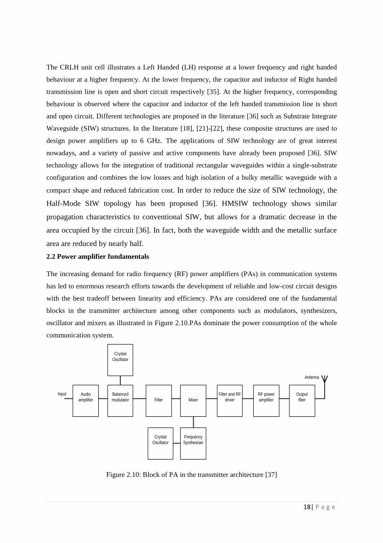
oscillator and mixers as illustrated in Figure 2.10.PAs dominate the power consumption of the whole
communication system.
Crystal
Oscillator
Audio
amplifier
Balanced
modulator Filter Mixer
Filter and RF
driver
RF power
amplifier
Output
filter
Frequency
Synthesiser
Crystal
Oscillator
Antenna
Input
Figure 2.10: Block of PA in the transmitter architecture [37]
Page 31
19| P a g e
Usually, the amplifier drives the antenna of the transmitter. The design targets of a power amplifier
usually include gain, output power, bandwidth, power efficiency and linearity. Taking into
consideration of these figures of performance, the device can be characterised.
In addition, modern power amplifies can operated in different modes or classes so as to achieve
specific targets.This classification represents the portion of the output signal that varies over a cycle
of operation considering a sinusoidal input signal. PAs can be classified into two categories, the
conduction angle and the switching mode classes of amplifiers.
2.2.1 Conduction angle classes of amplifiers
The power amplifier can be classified by the controlled conduction angle of the transistor that is
defined by the length of the conduction state over a portion of the output signal where the transistor
operates between ON and OFF states. Common amplifier classes are A, B, AB and C. Theoretically,
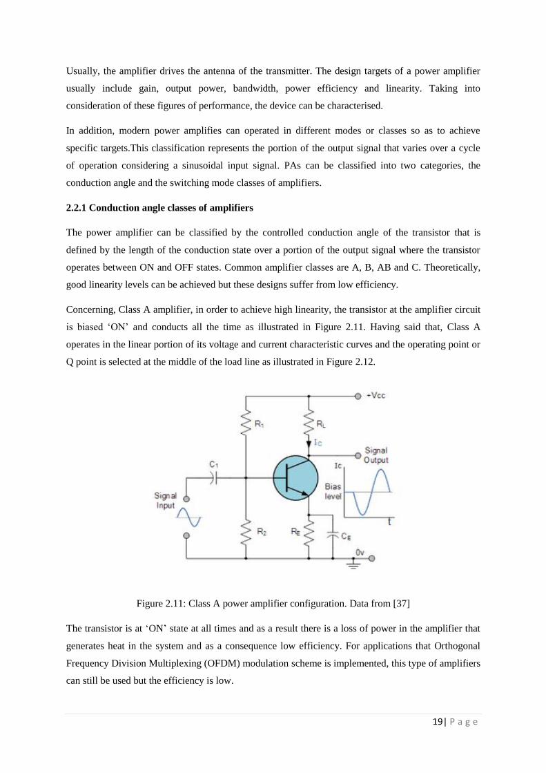
good linearity levels can be achieved but these designs suffer from low efficiency.
Concerning, Class A amplifier, in order to achieve high linearity, the transistor at the amplifier circuit
is biased ‘ON’ and conducts all the time as illustrated in Figure 2.11. Having said that, Class A
operates in the linear portion of its voltage and current characteristic curves and the operating point or
Q point is selected at the middle of the load line as illustrated in Figure 2.12.
Figure 2.11: Class A power amplifier configuration. Data from [37]
The transistor is at ‘ON’ state at all times and as a result there is a loss of power in the amplifier that
generates heat in the system and as a consequence low efficiency. For applications that Orthogonal
Frequency Division Multiplexing (OFDM) modulation scheme is implemented, this type of amplifiers
can still be used but the efficiency is low.
Page 32
20| P a g e
Figure 2.12: I-V characteristics [37]
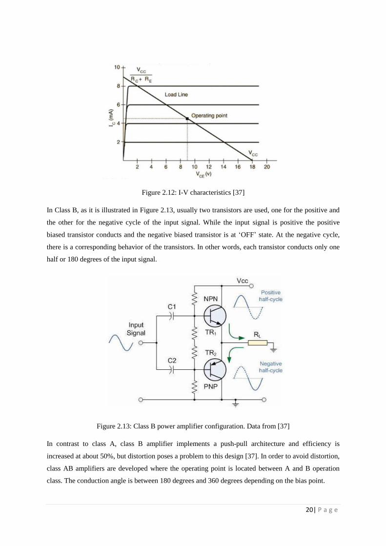
In Class B, as it is illustrated in Figure 2.13, usually two transistors are used, one for the positive and
the other for the negative cycle of the input signal. While the input signal is positive the positive
biased transistor conducts and the negative biased transistor is at ‘OFF’ state. At the negative cycle,
there is a corresponding behavior of the transistors. In other words, each transistor conducts only one
half or 180 degrees of the input signal.
Figure 2.13: Class B power amplifier configuration. Data from [37]
In contrast to class A, class B amplifier implements a push-pull architecture and efficiency is
increased at about 50%, but distortion poses a problem to this design [37]. In order to avoid distortion,
class AB amplifiers are developed where the operating point is located between A and B operation
class. The conduction angle is between 180 degrees and 360 degrees depending on the bias point.
Page 33
21| P a g e
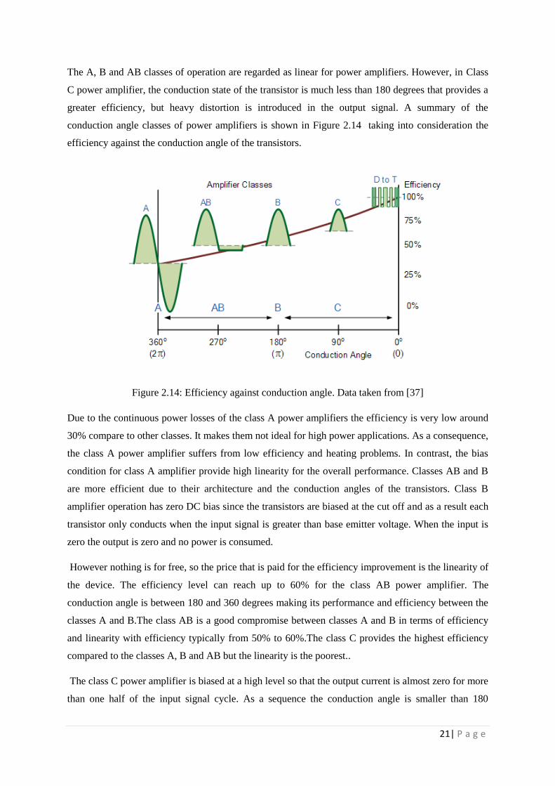
The A, B and AB classes of operation are regarded as linear for power amplifiers. However, in Class
C power amplifier, the conduction state of the transistor is much less than 180 degrees that provides a
greater efficiency, but heavy distortion is introduced in the output signal. A summary of the
conduction angle classes of power amplifiers is shown in Figure 2.14 taking into consideration the
efficiency against the conduction angle of the transistors.
Figure 2.14: Efficiency against conduction angle. Data taken from [37]
Due to the continuous power losses of the class A power amplifiers the efficiency is very low around
30% compare to other classes. It makes them not ideal for high power applications. As a consequence,
the class A power amplifier suffers from low efficiency and heating problems. In contrast, the bias
condition for class A amplifier provide high linearity for the overall performance. Classes AB and B
are more efficient due to their architecture and the conduction angles of the transistors. Class B
amplifier operation has zero DC bias since the transistors are biased at the cut off and as a result each
transistor only conducts when the input signal is greater than base emitter voltage. When the input is
zero the output is zero and no power is consumed.
However nothing is for free, so the price that is paid for the efficiency improvement is the linearity of
the device. The efficiency level can reach up to 60% for the class AB power amplifier. The
conduction angle is between 180 and 360 degrees making its performance and efficiency between the
classes A and B.The class AB is a good compromise between classes A and B in terms of efficiency
and linearity with efficiency typically from 50% to 60%.The class C provides the highest efficiency
compared to the classes A, B and AB but the linearity is the poorest..
The class C power amplifier is biased at a high level so that the output current is almost zero for more
than one half of the input signal cycle. As a sequence the conduction angle is smaller than 180
Page 34
22| P a g e
degrees, approximately 90 degrees area. The power amplifier can achieve a higher efficiency levels
around 80%. However, Class C biasing methodology and technique introduces much distortion of the
output signal making this class unsuitable for audio and RF applications [13]. There are also other
conduction angle power amplifier classes such as D or T but are not studied at this project and thesis.
2.2.2 Switching mode amplifiers
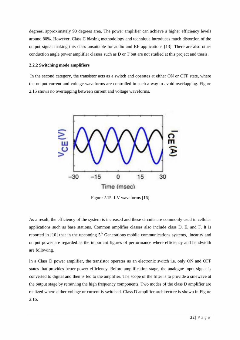
In the second category, the transistor acts as a switch and operates at either ON or OFF state, where
the output current and voltage waveforms are controlled in such a way to avoid overlapping. Figure
2.15 shows no overlapping between current and voltage waveforms.
Figure 2.15: I-V waveforms [16]
As a result, the efficiency of the system is increased and these circuits are commonly used in cellular
applications such as base stations. Common amplifier classes also include class D, E, and F. It is
reported in [10] that in the upcoming 5th Generations mobile communications systems, linearity and
output power are regarded as the important figures of performance where efficiency and bandwidth
are following.
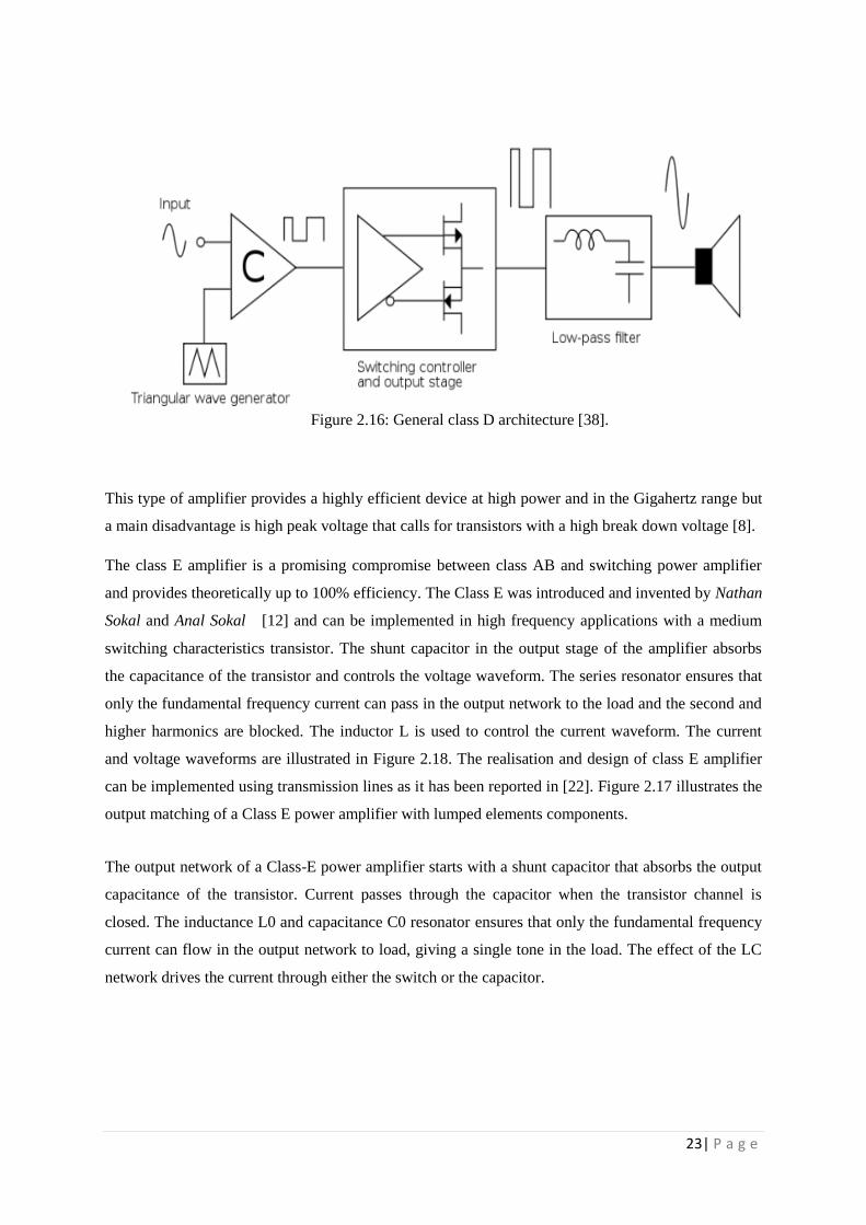
In a Class D power amplifier, the transistor operates as an electronic switch i.e. only ON and OFF
states that provides better power efficiency. Before amplification stage, the analogue input signal is
converted to digital and then is fed to the amplifier. The scope of the filter is to provide a sinewave at
the output stage by removing the high frequency components. Two modes of the class D amplifier are
realized where either voltage or current is switched. Class D amplifier architecture is shown in Figure
2.16.
Page 35
23| P a g e
Figure 2.16: General class D architecture [38].
This type of amplifier provides a highly efficient device at high power and in the Gigahertz range but
a main disadvantage is high peak voltage that calls for transistors with a high break down voltage [8].
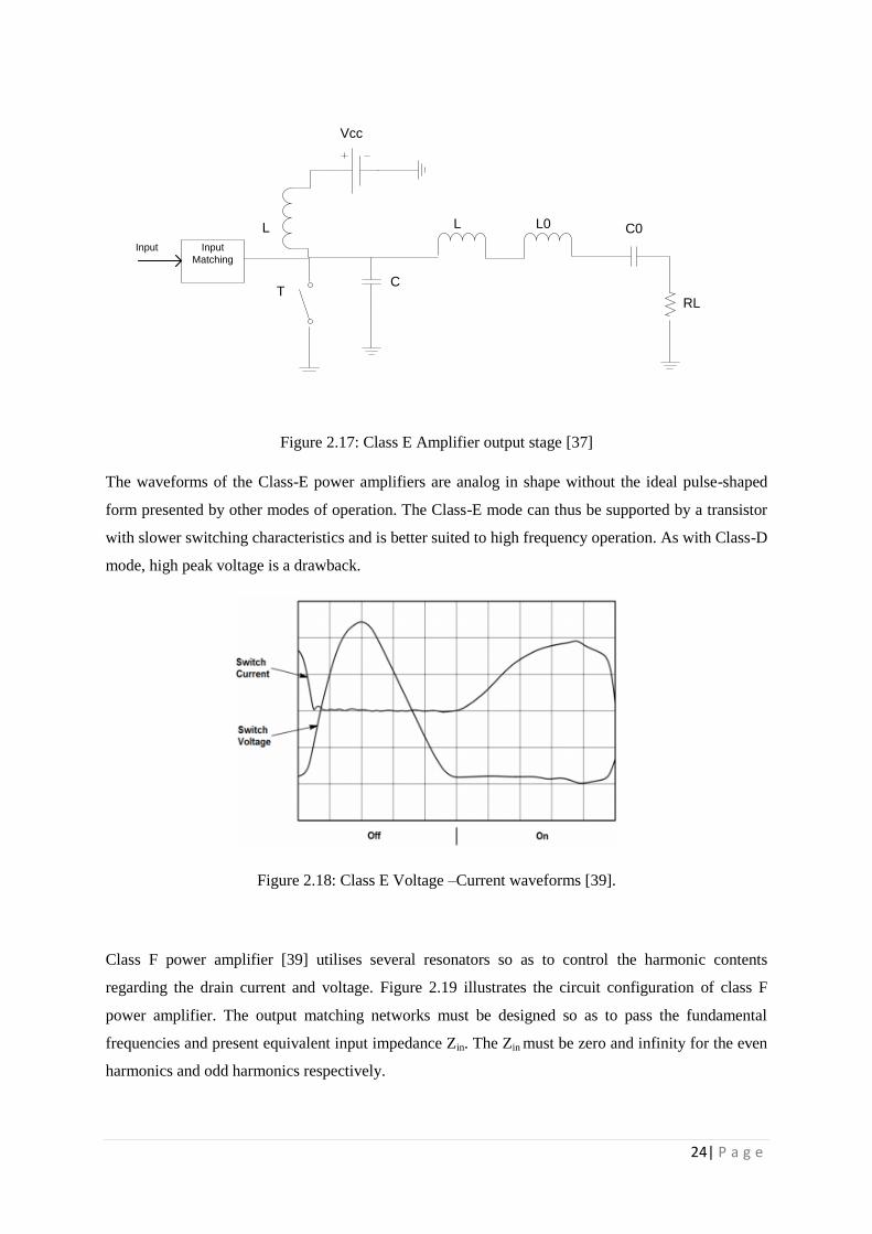
The class E amplifier is a promising compromise between class AB and switching power amplifier
and provides theoretically up to 100% efficiency. The Class E was introduced and invented by Nathan
Sokal and Anal Sokal [12] and can be implemented in high frequency applications with a medium
switching characteristics transistor. The shunt capacitor in the output stage of the amplifier absorbs
the capacitance of the transistor and controls the voltage waveform. The series resonator ensures that
only the fundamental frequency current can pass in the output network to the load and the second and
higher harmonics are blocked. The inductor L is used to control the current waveform. The current
and voltage waveforms are illustrated in Figure 2.18. The realisation and design of class E amplifier
can be implemented using transmission lines as it has been reported in [22]. Figure 2.17 illustrates the
output matching of a Class E power amplifier with lumped elements components.
The output network of a Class-E power amplifier starts with a shunt capacitor that absorbs the output
capacitance of the transistor. Current passes through the capacitor when the transistor channel is
closed. The inductance L0 and capacitance C0 resonator ensures that only the fundamental frequency
current can flow in the output network to load, giving a single tone in the load. The effect of the LC
network drives the current through either the switch or the capacitor.
Page 36
24| P a g e
C0
Vcc
L0LL
CT
RL
Input
Matching
Input
Figure 2.17: Class E Amplifier output stage [37]
The waveforms of the Class-E power amplifiers are analog in shape without the ideal pulse-shaped
form presented by other modes of operation. The Class-E mode can thus be supported by a transistor
with slower switching characteristics and is better suited to high frequency operation. As with Class-D
mode, high peak voltage is a drawback.
Figure 2.18: Class E Voltage –Current waveforms [39].
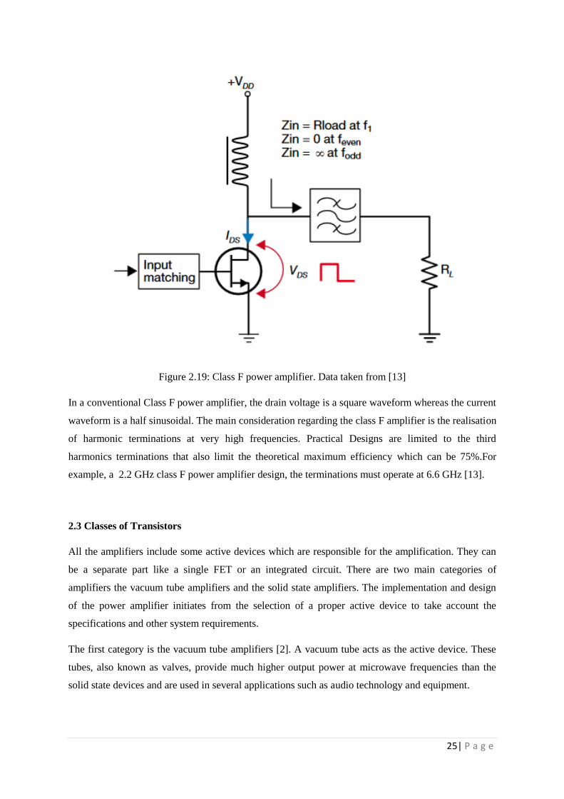
Class F power amplifier [39] utilises several resonators so as to control the harmonic contents
regarding the drain current and voltage. Figure 2.19 illustrates the circuit configuration of class F
power amplifier. The output matching networks must be designed so as to pass the fundamental
frequencies and present equivalent input impedance Zin. The Zin must be zero and infinity for the even
harmonics and odd harmonics respectively.
Page 37
25| P a g e
Figure 2.19: Class F power amplifier. Data taken from [13]
In a conventional Class F power amplifier, the drain voltage is a square waveform whereas the current
waveform is a half sinusoidal. The main consideration regarding the class F amplifier is the realisation
of harmonic terminations at very high frequencies. Practical Designs are limited to the third
harmonics terminations that also limit the theoretical maximum efficiency which can be 75%.For
example, a 2.2 GHz class F power amplifier design, the terminations must operate at 6.6 GHz [13].
2.3 Classes of Transistors
All the amplifiers include some active devices which are responsible for the amplification. They can
be a separate part like a single FET or an integrated circuit. There are two main categories of
amplifiers the vacuum tube amplifiers and the solid state amplifiers. The implementation and design
of the power amplifier initiates from the selection of a proper active device to take account the
specifications and other system requirements.
The first category is the vacuum tube amplifiers [2]. A vacuum tube acts as the active device. These
tubes, also known as valves, provide much higher output power at microwave frequencies than the
solid state devices and are used in several applications such as audio technology and equipment.
Page 38
26| P a g e
The second category regards with the transistor amplifiers that are commonly used today. A transistor
acts as the active device and the gain of the amplification depends on the many parameters. Numerous
applications are found and common examples include radio transmitters, audio and stereo amplifier
systems and mobile communications.
The key advantages of transistors that have replaced vacuum tubes are [3]:
Smaller size and weigh that reduce the equipment size in most of microwave and RF
applications.
Smaller operating voltages that can potentially reduce the power consumption of the device.
Reliability and longer lifetime compared to vacuum tubes that degrade and fail over time.
The amplification based on the transistor functionality is realised based on several configurations. For
instance a bipolar transistor can realize common collector, common base and common emitter
whereas the MOSFET transistor can realize common source, common gate and common drain with
respect to bipolar configuration [40].
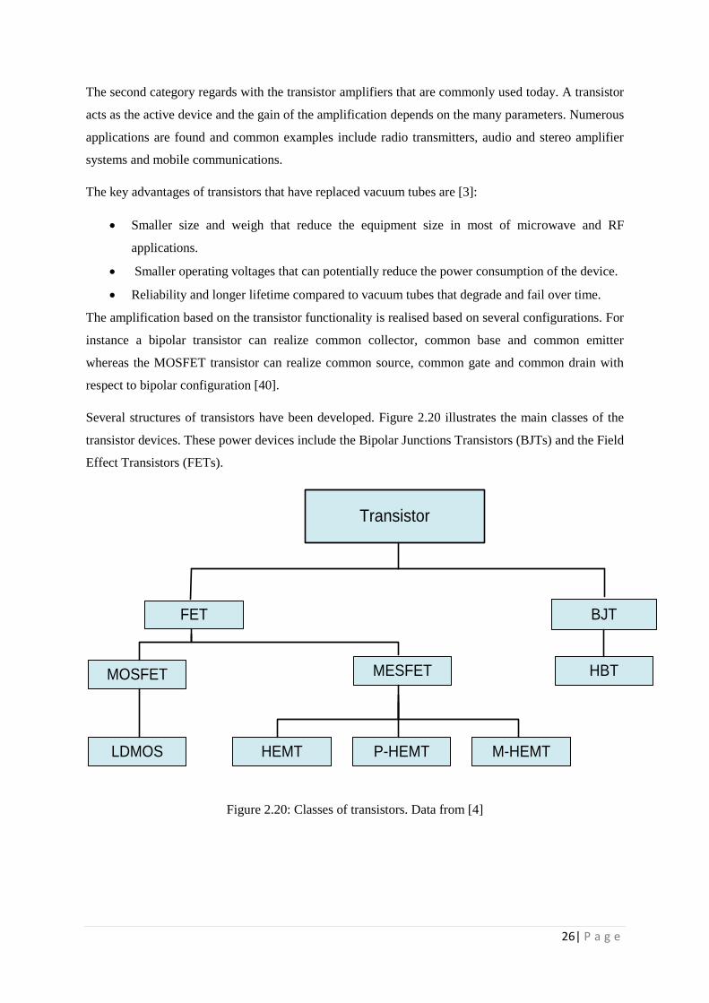
Several structures of transistors have been developed. Figure 2.20 illustrates the main classes of the
transistor devices. These power devices include the Bipolar Junctions Transistors (BJTs) and the Field
Effect Transistors (FETs).
Transistor
BJTFET
MOSFET MESFET
LDMOS HEMT P-HEMT
HBT
M-HEMT
Figure 2.20: Classes of transistors. Data from [4]
Page 39
27| P a g e
Field Effect Transistor (FETs) can be used in order to replace the normal Bipolar Junction Transistors.
A comparison of the advantages and disadvantages between these two categories are shown in the
Table 2.1.
Table 2.1: FET and BJT comparison [40]
Field Effect Transistors (FETs) Bipolar Junction Transistors(BJTs)
Low voltage gain High voltage gain
Low noise generation Medium noise generation
Fast switching time Medium switching time
Expensive and difficult to bias Cheap and easy to bias
Bipolar Junction Transistors (BJTs) and Field Effect Transistors (FETs) are mainly used in the design
of amplifiers, oscillators and switches. The BJTs are characterized by their low input impedance but
these are noisy devices because of the high minority carries taking into consideration the P-N-P and
N-P-N types of BTJs [40].
Due to the leakage current, the thermal stability is worse compared to FETs. In contrast to BJTs, the
FETs are referred as unipolar transistors because the charge carriers that carry the current through the
device are the same type, either holes or electrons but not both. FETs are quite immune to radiation
and are less noisy compare to BJTs that are very sensitive. FETs provide better thermal stability and
performance than BJTs but in many cases they have smaller gain bandwidth.
Subcategories of FETs include the Metal Oxide Semiconductor Field Effect Transistors (MOSFETs)
and Metal Semiconductor Field Effect Transistors (MESFETs). They are usually more expensive
compared to the aforementioned but have faster switching capability. They can operate up to 45 GHz
and they are good candidates for RF and microwave applications such as radar and satellite
communications. High quality surface materials are used in this technology such as GaAs and GaN
[40].
Transistors have played a key role in the development of communications electronics such as power
amplifiers and oscillators. Numerous investigations have been conducted for the evolution of
transistors. Essentially the design of a power amplifier starts with the selection of the appropriate
device and the set of specifications.
The proper and best candidate for each application depends on a series of parameters and design
specification such as the pre-defined and desired output power level and the operational frequency
Page 40
28| P a g e
bands. Among the suitable candidates for the design of power amplifiers are the GaN High Electron
Mobility Transistor (HEMT) due to the inherent advantages.
2.4 Selection of transistor
The active device is selected according to its functionalities and characteristics that are related to the
design specifications and device’s limitations. There are many transistor devices as it has been
observed in the literature review and design examples. In addition, several technologies are suitable
for specific applications. Concerning the options for the design of dual band amplifiers in case of
wireless communications and infrastructure such as base station (BSs) the Gallium Nitride (GaN)
High Electron Mobility Transistor (HEMT) is a perfect candidate due to its advantages of higher
efficiency, power density and larger bandwidth [69]-[70]. Table 2.2 summarises the transistor’s
specifications.
Table 2.2: CREE Transistor’s specifications [67]
Transistor features
Peak output power 10W
Frequency range DC – 6 GHz
Operating Voltage 28V
Package type Flange/Pill
The proposed design concerns the implementation of Class E power amplifier and thus HEMT
technology is used because of the high switching time and efficiency. As it is well known, class E
incorporates transistors in a switch mode operation [71].
The RF GaN HEMT power transistor from CREE is selected for general purpose broadband
applications. It adheres to requirements and specifications of designs. This particular transistor can
operate from DC up to 6 GHz and the available output power is 10 W. In addition, it offers high
efficiency, gain and wide bandwidth making it ideal for linear amplifier circuits.
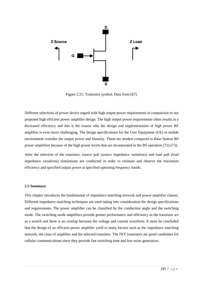
The transistor is already packaged and it is appropriate for the design of the layout and the fabrication.
Figure 2.21 illustrates the electrical symbol of the MESFET transistor. The impedance at the gate of
the transistor or ZSource must match to the input of the power amplifier whereas the output impedance
ZLoad to the output stage of the amplifier.
Page 41
29| P a g e
Figure 2.21: Transistor symbol. Data from [67].
Different selections of power device regard with high output power requirements in comparison to our
proposed high efficient power amplifier design. The high output power requirements often results in a
decreased efficiency and this is the reason why the design and implementation of high power RF
amplifier is even more challenging. The design specifications for the User Equipment (UE) in mobile
environment consider the output power and linearity. These are modest compared to Base Station BS
power amplifiers because of the high power levels that are incorporated in the BS operation [72]-[73].
After the selection of the transistor, source pull (source impedance variations) and load pull (load
impedance variations) simulations are conducted in order to estimate and observe the maximum
efficiency and specified output power at specified operating frequency bands.
2.5 Summary
This chapter introduces the fundamental of impedance matching network and power amplifier classes.
Different impedance matching techniques are used taking into consideration the design specifications
and requirements. The power amplifier can be classified by the conduction angle and the switching
mode. The switching mode amplifiers provide greater performance and efficiency as the transistor act
as a switch and there is no overlap between the voltage and current waveform. It must be concluded
that the design of an efficient power amplifier yield to many factors such as the impedance matching
network, the class of amplifier and the selected transistor. The FET transistors are good candidates for
cellular communications since they provide fast switching time and low noise generation.
Page 42
30| P a g e
CHAPTER
Dual band designs
3 -----------------------------------------------------------------------------------------------------------------
This chapter is divided into two sections. The first section of the chapter concerns the different
designs that are implemented in the realisation of matching networks and more specifically for dual
band designs. The second section concerns with the review that has been conducted for the design of
a concurrent dual band power amplifier at different frequency bands and especially cellular bands.
Several methods have been studied from conventional matching networks to Composite Right Left
Handed (CRLH) transmission lines implementations. A summary table follows to compare the
performance and functionality of the power amplifier architectures.
3.1 Dual band matching networks
One of the procedures to design an efficient power amplifier requires matching networks at the input
and output stage. At this subsection, there is an investigation of different types of matching networks
designs that are used in the design of dual band power amplifiers.
3.1.1 Dual band impedance matching using resonators
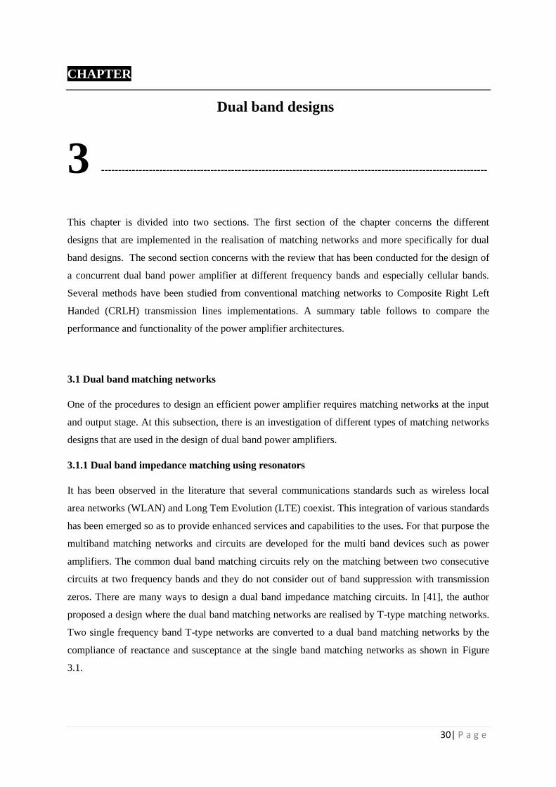
It has been observed in the literature that several communications standards such as wireless local
area networks (WLAN) and Long Tem Evolution (LTE) coexist. This integration of various standards
has been emerged so as to provide enhanced services and capabilities to the uses. For that purpose the
multiband matching networks and circuits are developed for the multi band devices such as power
amplifiers. The common dual band matching circuits rely on the matching between two consecutive
circuits at two frequency bands and they do not consider out of band suppression with transmission
zeros. There are many ways to design a dual band impedance matching circuits. In [41], the author
proposed a design where the dual band matching networks are realised by T-type matching networks.
Two single frequency band T-type networks are converted to a dual band matching networks by the
compliance of reactance and susceptance at the single band matching networks as shown in Figure
3.1.
Page 43
31| P a g e
Figure 3.1: Dual band impedance matching networks using resonators. Data from [41].
The specific design and technique is implemented in a power amplifier configuration at 881 MHz and
2.14 GHz.
3.1.2 T-type dual band matching using coupled line
The design of dual band and multi band networks and devices can be quite complex. It has been
reported in [42], [43] that matching circuits can be realised by the implementation of dual band
Chebyshev impedance transformer. This technique is valid in the case that the source and load are real
impedances and it provides a matching when the load impedance is complex and frequency dependent
as in the case of a general dual band amplifier that the transistor operation regards with two different
complex impedances at the two different frequencies. However, it has been reported in [44] a
methodology and design approach to realise matching of two arbitrary complex load impedances but
this method is not suitable and not accurate when the complex loads impedances are frequency
dependent.
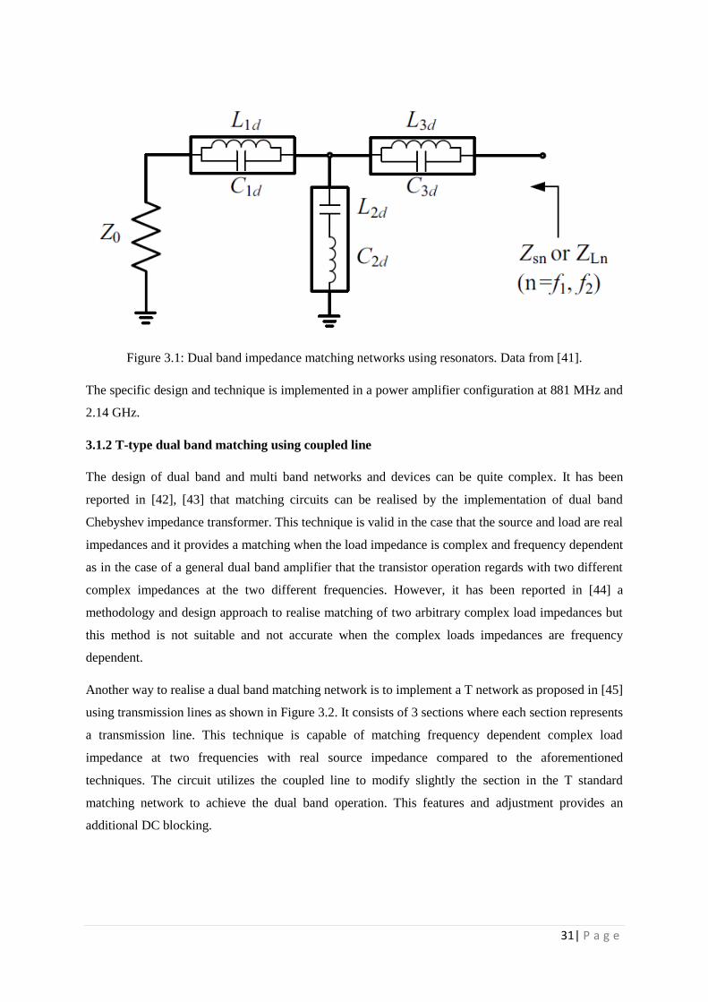
Another way to realise a dual band matching network is to implement a T network as proposed in [45]
using transmission lines as shown in Figure 3.2. It consists of 3 sections where each section represents
a transmission line. This technique is capable of matching frequency dependent complex load
impedance at two frequencies with real source impedance compared to the aforementioned
techniques. The circuit utilizes the coupled line to modify slightly the section in the T standard
matching network to achieve the dual band operation. This features and adjustment provides an
additional DC blocking.
Page 44
32| P a g e
Figure 3.2: Dual band impedance matching networks. Data from [45]
As it is observed, the overall matching network has a T-type configuration where the section A and C
consists of a transmission line with an appropriate characteristic impedance and electrical length
whereas the section B consists of a coupled line with even and odd mode impedances Ze and Zo [46]
respectively with their appropriate electrical length to realise dual band operation.
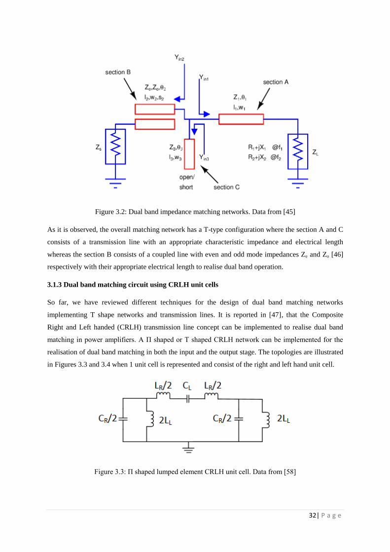
3.1.3 Dual band matching circuit using CRLH unit cells
So far, we have reviewed different techniques for the design of dual band matching networks
implementing T shape networks and transmission lines. It is reported in [47], that the Composite
Right and Left handed (CRLH) transmission line concept can be implemented to realise dual band
matching in power amplifiers. A Π shaped or T shaped CRLH network can be implemented for the
realisation of dual band matching in both the input and the output stage. The topologies are illustrated
in Figures 3.3 and 3.4 when 1 unit cell is represented and consist of the right and left hand unit cell.
Figure 3.3: Π shaped lumped element CRLH unit cell. Data from [58]
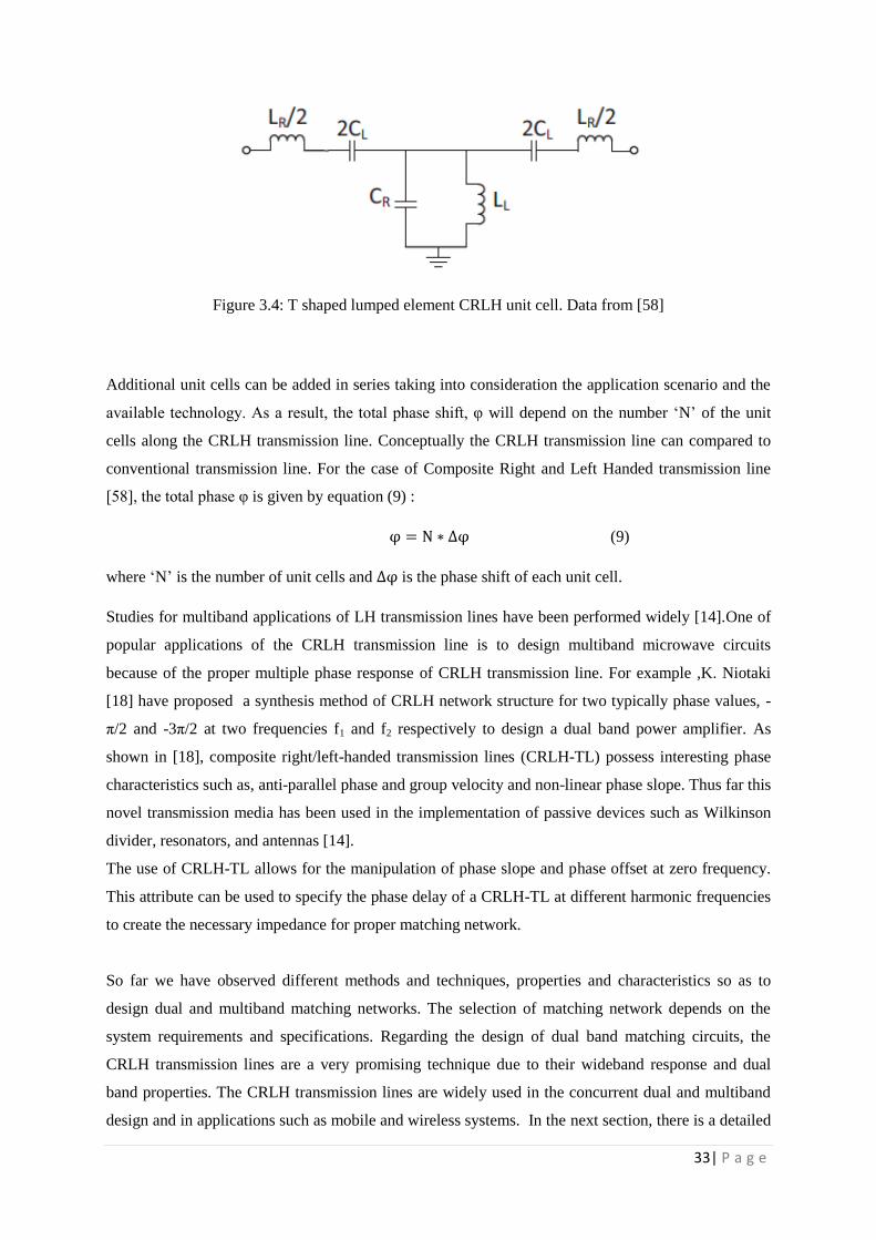
Page 45
33| P a g e
Figure 3.4: T shaped lumped element CRLH unit cell. Data from [58]
Additional unit cells can be added in series taking into consideration the application scenario and the
available technology. As a result, the total phase shift, φ will depend on the number ‘N’ of the unit
cells along the CRLH transmission line. Conceptually the CRLH transmission line can compared to
conventional transmission line. For the case of Composite Right and Left Handed transmission line
[58], the total phase φ is given by equation (9) :
φ = N ∗ ∆φ (9)
where ‘N’ is the number of unit cells and ∆φ is the phase shift of each unit cell.
Studies for multiband applications of LH transmission lines have been performed widely [14].One of
popular applications of the CRLH transmission line is to design multiband microwave circuits
because of the proper multiple phase response of CRLH transmission line. For example ,K. Niotaki
[18] have proposed a synthesis method of CRLH network structure for two typically phase values, -
π/2 and -3π/2 at two frequencies f1 and f2 respectively to design a dual band power amplifier. As
shown in [18], composite right/left-handed transmission lines (CRLH-TL) possess interesting phase
characteristics such as, anti-parallel phase and group velocity and non-linear phase slope. Thus far this
novel transmission media has been used in the implementation of passive devices such as Wilkinson
divider, resonators, and antennas [14].
The use of CRLH-TL allows for the manipulation of phase slope and phase offset at zero frequency.
This attribute can be used to specify the phase delay of a CRLH-TL at different harmonic frequencies
to create the necessary impedance for proper matching network.
So far we have observed different methods and techniques, properties and characteristics so as to
design dual and multiband matching networks. The selection of matching network depends on the
system requirements and specifications. Regarding the design of dual band matching circuits, the
CRLH transmission lines are a very promising technique due to their wideband response and dual
band properties. The CRLH transmission lines are widely used in the concurrent dual and multiband
design and in applications such as mobile and wireless systems. In the next section, there is a detailed
Page 46
34| P a g e
literature review for the dual band power amplifier design and different techniques that are
implemented to obtain the dual band operation, performance and responses as well as to increase the
efficiency and other figures of merit of performance for the overall system.
3.2 Dual band power amplifiers
The trends have been investigated in the chapter 1 regarding the design of modern dual and multiband
power amplifier for the concurrent operation and performance, where there is an amplification of the
signal at the two or multi frequency bands simultaneously. In the literature review, we have observed
several ways to design a dual band power amplifier. Among them, the most widely used is the
Doherty power amplifier [52] configuration that is found essentially in mobile communications due to
the fact that this type provides a good relationship and trade-off between linearity and efficiency. At
this subsection, there is an investigation of different types of designs that are used in the design of
dual band power amplifiers.
Literally, five designs of dual band power amplifier are studied and compared. These are the
following:
Dual band power amplifier based on two frequency matching.
Dual band amplifier design with diplexer.
Concurrent Doherty amplifier.
Dual band power amplifier based on Compact Microstrip Resonant Cell CMRCs.
Dual band amplifier using CRLH matching networks.
3.2.1 Dual band power amplifier based on two frequency matching
A method to design dual band operation is described in [48] and [49] and is based on the low pass
Chebyshev impedance transformer. Two mobile frequencies at 800 MHz and 1.5 GHz are considered
as the two frequency bands of operation. In this work, GaAs Field effect Transistor (FET) in Class AB
class of amplifier is implemented. One of the design requirements for the mobile and wireless
commutations systems is the linearity. The Class AB provides a good trade-off between the linearity
and systems efficiency of the system as it is used very often in the literature and many other similar
designs.
In order to realise the matching networks at input and the output stage, the values of these circuit
elements are determined by the impedance transformation circuit design tables as reported in [50].The
low pass Chebyshev impedance transformer and its frequency response are illustrated in Figure 3.5.
Page 47
35| P a g e
The low pass Chebyshev impedance transformer generates N frequencies where N corresponds to the
number of the stages in the transformer and impedance is matched at these amplification bands.
Figure 3.5: Two stage Chebyshev low pass impedance transformer and its frequency response [15].
Figure 3.6: Circuit configuration of dual band GaAs FET power amplifier [15].
Figure 3.6 represents the complete dual band power amplifier topology as well as the input and the
output matching network implement the low pass Chebyshev transformer. Regarding this particular
design method, several requirements such as gain, bandwidth and efficiently are imposed and further
developments of these figures are needed in order to achieve the latest specifications.
Page 48
36| P a g e
3.2.2 Dual band amplifier design with diplexer
Another method that has been regularly used is the design of dual band amplifier based on diplexers
[51] as illustrated in Figure 3.7.
Figure 3.7: Dual band power amplifier design with diplexer [51].
The power amplifier is designed and implemented for a concurrent dual band operation, suitable for
mobile 3rd
Generation (3G) Wideband Code Division Multiple Access (WCDMA) at 1.9GHz and
Worldwide interoperability for Microwave Access (WiMAX) digital systems at 3.4GHz.Concerning
this particular architecture, the diplexer acts as passive device and presents a critical component in the
overall circuit. This component must ensure that there are no loss in the transmission path and provide
a good isolation. It is used to test the amplifier under large signal conditions and offers an insertion
loss of 0.6 dB and 0.8dB for the two bands respectively and isolation between the channels.
The matching network is considered for the design of the power amplifier and it is a vital part of the
structure. Π type matching network architecture is implemented. The selected Π type technology
inserts a null in the transfer function in the transfer characteristic curve between the two frequencies.
Similar to previous design, the Class AB is utilized in the design to provide a good trade-off between
linearity and efficiency.
Page 49
37| P a g e
3.2.3 Concurrent Doherty amplifier
In comparison to the other designs, Doherty Amplifier is capable of improving the efficiently of the
system. It is able to accommodate signals with high Peak to Average Power Ratio (PARP) such as
OFDM and consists of two amplifiers [52], [53] as it is shown in Figure 3.8, the “main” or the
“carrier” and the “peaking” amplifier. The carrier amplifier operates usually in class AB and is used to
carry the average signals levels. Regarding the high power levels, the peaking is implemented to deal
with these higher levels, where it is biased at class C and provides extra power capability that carrier
amplifier cannot.
Figure 3.8: Dual band Doherty amplifier. Data taken from [52].
This particular structure requires a splitter and a combiner so as to allow the power to be splitted of
the amplifiers and summed at the output stage. The proposed design implements T type matching
networks in the input and output stage to realise the dual band impedance transformer and phase
shifter simultaneously. The operating frequencies are mobile frequencies, particularly 900MHz and
2GHz. The improvement of the efficiency taking into account the Doherty power amplifier is due to
the load pull effect [54] by using quarter wavelength, λ/4 transmission lines. The MESFET transistor
technology is implemented.
The advantages of the Doherty power amplifier are summarized in the Table 3.1.
Table 3.1: Advantages and Disadvantages of Doherty Amplifier.
Advantages Disadvantages
Higher efficiency[55] Phase shifts of splitters are difficult to maintain
Suitable for envelope tracking [54],[55] Higher design cost
Page 50
38| P a g e
3.2.4 Dual band power amplifier based on Compact Microstrip Resonant Cell (CMRCs) .
At this specific work [56], the authors presented a quite new design that is different from the
aforementioned ones in previous sections. The design regards with the multi harmonic control circuit
implementing cascaded Compact Microstrip Resonant Cells (CMRCs) [56].Such kind of structure is
employed to realize right and left handed structures and it is used to achieve slow wave (large
propagation constant) in order to reduce the physical size of microwave components. With specific
patterns etched on the microstrip line, these cells exhibit different characteristics of slow wave and
band stop. Several frequencies can be terminated simultaneously due to these compact structures and
provide low pass characteristics and slow wave effects [57]. The dual band power amplifier design
implements class F configuration that operates at 2.4 and 3.5 GHz. The efficiency is almost 70 % and
63% for the lower and upper band respectively with a power level greater than 33 dBm for both
frequency bands. Figure 3.9 illustrates the Class F power amplifier configuration and design based on
CMRCs.
Figure 3.9: Dual band power amplifier based on CMRCs. Data from [56].
As it is observed from the Figure 3.9, the harmonic control has been developed by cascading two
compact microstrip resonant cells CMRCs and a shunt capacitor. The second and the third harmonic
of the two operating bands are terminated by the CMRC before the dual band fundamental matching
circuit. Specific patterns and methodologies on the microstrip line have been conducted and these
cells provide different characteristics of slow wave and band stop that are used for the harmonic
terminations.
The first CMRC behaves as a low pass filter and the stop band is set to the third harmonic 3f0 at 10.5
GHz to reflect back the signal with a proper phase. In addition, there is a tuning line referred to as
Transmission Line (TL) 1 that is implemented in order to compensate the transistors parasitic. The
Page 51
39| P a g e
design considers the third harmonic of the lower frequency to be close to the second harmonic of the
upper frequency, as this can be terminated simultaneously by the second compact microstrip resonant
cell (CMRC) 2 whose stop band is located between 7.0 to 7.2 GHz.
3.2.5 Dual band amplifier using CRLH matching networks
The matching networks can be realised by implementing Composite right Left Handed (CRLH)
transmission lines. To realise a dual band operation, a CRLH unit cell can be used. It exhibits dual
band frequency response at two frequencies due to the phase characteristics [58], [59]. The process of
obtaining the values for the components for a dual band response based on CRLH transmission lines
is also reported in [60].
For the design of dual band power amplifier as it has been reported in [62], a HEMT transistor
technology is used as the active component in the power amplifier circuit. The presented approach is
easily applied in the design of matching networks to realize dual band operation at microwave
circuits. The efficiency and overall performance is regarded as the highest in comparison to the other
designs. These structures are used in our dual band design as they are good candidates for dual band
response and performance. A lot of the work concerns the design of dual band amplifiers in addition
to the conventional methods that are based on direct matching circuits such as Π and T matching
networks.
The design and realisation of matching networks based on CRLH transmissions lines has been
reviewed in the literature review [14]. As described in the [62], the implementation of CRLH
transmission lines are based on the lumped elements equivalent circuits. In [14], [21] the design of the
CRLH matching circuits is based on the circuit depicted in Figure 3.10. The Right Handed (RH)
transmission lines have been replaced by the conventional lossless transmission lines. This structure
represents the equivalent of the lumped element configuration as the transmission line as it does not
include the resistance R and conductance G.
`
2CL
Z0R,θR Z0R,θR2CL
LL
NL =1
Figure 3.10: CRLH transmission line. Data from [60].
Page 52
40| P a g e
As mentioned earlier, a CRLH transmission line consists of a right hand and left hand (phase delay)
transmission line. The dispersion characteristics of these are manipulated in a way that the desired
electrical length at any pair of frequencies is obtained.
In Figure 3.11, an example of CRLH transmission line is depicted. There are two right handed
transmission lines with Zor characteristic impedance and Θr electrical length in series with one left
handed unit cell in an equivalent lumped element configuration. The total phase response ΦC of a
CRLH transmission line [60] - [62] is the summation of phase responses of right and left handed
circuits and is given equation (10)
ΦC = ΦR + ΦL (10)
0
Frequency
(MHz)
Ph
ase
re
sp
on
se
(de
gre
es)
+
ΦC = ΦR + ΦL
- ΦR
ΦL
Figure 3.11: Phase response of Right and Left Handed transmission lines.
Composite Right Left-Handed (CRLH) transmission line possesses interesting phase characteristics
such as, anti-parallel phase and group velocity and non-linear phase slope. The use of CRLH
transmission line allows for manipulation of phase slope and phase offset at zero frequency. This
attribute can be used to specify the phase delay of a CRLH-TL at different harmonic frequencies to
create the required impedance for proper matching network. Using this method a CRLH transmission
line network can be used to match circuit components of dual mode class-E power amplifier. The
CRLH transmission line, which is the combination of a left-handed (LH) transmission line and a
right-handed (RH) transmission line, is proposed in [60]. The equivalent lumped elements model of
the LH transmission line exhibits positive phase response (phase lead). On the other hand, the RH
transmission line has negative phase response (phase lag). Therefore CRLH transmission line can
substitute for the matching network using microstrip lines.
At lower frequencies, the CRLH phase response approaches the Left Handed (LH) response curve due
to the negligible values of inductors and capacitors at the Right Handed (RH) that corresponds to
positives phase. At higher frequencies, the CRLH transmission line curve approaches the right handed
curve due to the negligible values of inductors and capacitors of Left handed TL that corresponds to
Page 53
41| P a g e
phase lag or negative phase. The CRLH transmission line phase curve can intercept a pair of
frequencies for dual band operation.
The equations for the calculation of the inductance L and capacitance C components in the left handed
transmission line and the electrical length considering the Right Handed (RH) transmission line are
illustrated in Matlab in Appendix 3.
The class E and F amplifier is used often in literature and in majority of designs for the wireless
systems so as to obtain higher efficiency. As mentioned in the introduction, in order to achieve a
proper class E operation, load impedances for fundamental frequencies and open circuit for second
harmonics are required
3.2.6 Comparison between power amplifier designs
Table 3.2 provides a comparison regarding the performance in terms of Power Added Efficiency
(PAE) and output power in dBm. It must be mentioned that the operating frequencies are different
among the aforementioned techniques and the figures of merit that are observed and compared,
concern the practical experiments and results from the fabrication process. The dual band design using
two frequency matching networks regarding the first method and the design considering the second
technique that is based on Π technology in conjunction with the insertion of the diplexer to realize
concurrent operation lead to almost the same efficiency and output power, taking into consideration
the fact that the same amplifier class AB is used. As a result, the PAE is at medium levels,
approximately 48% and 40 % respectively for the two methods. These type of matching circuits and
system architecture is suitable for wireless communications where linearity and efficiency must be
met at the same time. The power levels regarding the first two techniques are almost 25 dBm and 27
dBm for the upper and lower frequency band respectively. A more sophisticated method to increase
the efficiency and obtain a good linearity is to implement Doherty amplifier. The efficiency is
increased by 18% compared to the other designs as well as the power levels that reach almost 1
W.The efficiency is further increased by implementing the CMRCs by almost 20%. At similar trend,
the output power is increased taking into account the operating frequency and the type of transistor
technology. Regarding CMRCs implementation, the measured efficiency has reached 63% and 68%
for the lower and the upper band respectively. The output power levels using CMRCs reach 35 dBm
and 33 dBm for the lower and upper band.
For the CRLH technique, the power levels approach higher levels, 36 dBm and 33 dBm for upper and
lower band respectively, compared to the CMRCs technique. The PAE is not measured at [62] due to
the fact that no switching mode class of amplifier is realized. Only the drain efficiency is calculated
and presented. Although the design of power amplifier with CRLH transmission lines provides good
drain efficiency, the design using CMRCs can achieve higher performance due to the lower pass
characteristics and slow wave effect of CRMC. It must be mentioned that the Class F amplifier has
Page 54
42| P a g e
been implemented in the case of the CMRC method. It provides the increment in the efficiency and
output power levels compared to the dual band CRLH design. In the last design, no amplification
class has been considered.
Table 3.2: Performance comparison
Technique Amplifier class Frequency band
(GHz)
PAE (%)
Output Power
(dBm)
Two frequency
matching [15]
AB 0.8/1.5 48.4/40.3 27.8/26.6
Diplexer and Π
matching [48]
AB 1.98/3.42 40/43 25/27
Doherty [49] Doherty
(Class AB and C)
0.9/2 59/61 29.8/30.4
Cascade
CMRCs[53]
F 2.4/3.5 63/68 35.6/33
CRLH matching
networks [62]
N/A 2.3/3.35 N/A
(65/60 Drain
Efficiency)
36/33
3.3 Summary
This chapter explains the different methods that are used in impedance matching network design and
power amplifier. Several dual band designs are compared. Although the power amplifier design using
Compact Microstrip Resonant Cells (CMRCs) provide good in trerms of efficiency and output power,
the Composite Right and Left Handed (CRLH) unit cells are the best candidates as their structure
exhibits a dual band frequency response at an arbitrary pair of frequencies because of its phase
characteristics.
Page 55
43| P a g e
CHAPTER
Experimental
4 ----------------------------------------------------------------------------------------------------------------
This chapter concerns the methodology and procedure so as to design the proposed dual band Class E
amplifier circuit at the specified operating frequencies bands taking into considerations the system
requirements and objectives. The design procedure is explained analytically in conjunction with the
load and source pull simulation and system configurations. A general approach on how to obtain dual
band reponse using the Composite Right Left Handed (CRLH) unit cells is discussed. Moreover, the
design and implementation of the input and the output matching networks as well as the bias networks
are discussed. Also there is a discussion for the harmonic balance analysis of the power amplifier.
4.1 Procedure
The design of power amplifier can be very difficult and especially dual and multiband power
amplifiers is quite challenging taking into account the design requirements and specifications. The
basic principles [63] regarding the design of power amplifier systems can be summarized in the
following steps below:
Design the Biasing networks and circuits
Stabilization considerations
Impedance Matching at the input stage
Impedance matching at the output stage.
Different techniques and methodologies [64] are used so as to provide a DC power supply to the main
component of the power amplifier, the transistor. Stabilization must be considered for the transistor
functionality to avoid oscillations. When the input and output reflection coefficients are greater than
unity the transistor is regarded as an oscillator [64]. The input and output matching networks may be
used to provide maximum power transfer from source to transistor and from transistor to load
respectively. At next section, there is a detailed explanation on how to design the dual band matching
networks based on CRLH transmission lines taking into consideration the switching mode Class E
amplification.
The block diagram in Figure 4.1 illustrates the procedural that is followed in order to design the dual
band power amplifier.
Page 56
44| P a g e
The procedure includes the following steps:
a) Perform load pull and source pull simulations to obtain optimal inout and output impedances in
the input and the output stage.
b) Obtain general dual band response based on CRLH transmission lines and calculation.
c) Convert the CRLH transmission lines to matching network using ABCD parameters.
d) Design of Class E amplifier with CRLH networks at input and output stages with the selected
active device.
e) Proceed with the fabrication process.
The design of the dual band circuit based on the CRLH transmission lines is adjusted according to the
values in the load pull simulations, the performance and overall efficiency of the amplifier. That is
why there is direct feedback at these stages as shown in Figure 4.1. The calculation of the equivalent
optimum impedance Zopt of the output matching network depends on ABCD and Z parameters [65].
The ABCD parameters are also known as chain or cascade transmission line parameters and their
implementation is preferred to represent a cascade of two ports with the matrices equivalent that are
considered in the same order that a network diagram would be draw from left to right. After the
calculation of the ABCD parameters, the Z parameters are calculated so as to compute the equivalent
impedance of the input and the output matching networks. The CRLH transmission lines are used in
order to match the optimal impedance from source pull and load pull simulation to 50 Ω ports.
The load pull simulation [66] is conducted to estimate at what load impedance, maximum efficiency
and output power is achieved. There is a compromise among these figures of performance.
Consequently, after the determination and design of the output matching networks, the next stage of
the procedure is to design the input matching networks taking into account the output matching
network. As a result source pull simulations are conducted to estimate the optimal input impedances
and provide the optimal performance and efficiency of the power amplifier. The source pull
simulations are conducted with the calculated output matching networks at the output stage. The load
pull simulation, as it is described in next sections, for the selected transistor [67] has been conducted
and the optimal impedance is:
Zopt=39+26j (Ω)
It is important and convenient that the Zopt is almost the same for both the lower f1 and higher
frequency band f2.The equivalent input impedance of the CRLH matching network must be adjusted
to the Zopt so there are modifications and adjustments in the CRLH networks such as the phase
difference between the f1 and f2 and the number of unit cells at the right and left handed transmission
lines. The same procedure is also conducted in the input stage following the previous methodology,
considering source pull simulations [68], [69] instead of load pull.
Page 57
45| P a g e
Select an approproate
transistor type and technology
Obtain efficient Class E
Dual band Amplification
response
Dual Band repsonse based on
CRLH transmission line
Design Class E Amplifier
operation based on CRLH
transmission lines
Perform Load pull simulations to observe
the optimal impedance for maximum
efficiency
Perform Source Pull
Simulations to observe input
impedances
Figure 4.1: Procedural diagram.
4.2 Load pull and source pull simulations.
Load pull analysis is used to construct of contours that determine the maximum performance
achievable at a given load impedance. These contours are important to assess the actual impedance
that a device should see while it is used in amplifier. The closest match at the output is found for the
optimal output impedance. The output impedances are changed and the tuner is adjusted to provide
conjugate matching and thus constant input power. This is repeated as many times as possible. For
each output power point, a set of loci is generated that provide the impedances and the power. Same
principles apply to source pull simulations. The load pull is a technique that is applied to the Device
Under Test (DUT) where the load impedance is varied systematically. The DUT is the active device
or the transistor and load pull simulations are conducted to assess its properties and behavior so as to
deliver maximum efficiency and performance in the topology and system. The load pull simulations
have been conducted using the Agilent Advanced Design System (ADS) software.Regarding the
functionality of the transistor, the positive bias voltage is 28 V at the drain of the transistor and the
negative -3 V at the gate of the transistor. Load pull simulations are conducted as illustrated in Figure
4.2.The load impedance at the output stage is varied so as to obtain the maximum performance. At 28
V of transistor bias, the output capacitance of the transistor is almost 1.3pF from [67] and as a result
the extra parallel capacitance is deactivated as shown in Figure 4.2.
Page 58
46| P a g e
Load
Impedance
Parallel
capacitor
deactivated
Figure 4.2: Load Pull configuration.
All the simulated load impedances are shown within the Smith Chart in the Figure 4.3.100 points are
simulated in Smith Chart and shown in the figure 4.13.The data is taken from the Agilent ADS
software tool. As it can be observed from the Smith Chart, the center of the circle is set to 0+0j as
initially the point of optimal impedance is not known. The radius is set to 0.95 in the Smith Chart so
as to cover the entire circle and obtain the location of the optimal impedance. Τhe output matching
networks is completely deactivated and shorted in the simulations. Due to the fact that the number of
ports is quite large, the transistor provides maximum precision and accuracy at multiples of hundreds
of frequency. The load pull simulations are conducted for 450MHz and 700 MHz. The optimal
impedance at the output stage Zopt for both the lower and the higher frequency is:
Zopt=39+26j (Ω)
Figure 4.3: Simulated load impedances. Data from Agilent ADS simulations
Appendix 1 illustrates the power contours and optimal load impedances for the load pull simulations
that are obtained in Agilent ADS for both the lower and the upper frequency band, 450 MHz and 700
MHz respectively. The delivered power contours represent the magnitude of the input reflection
coefficient S11.At this load impedance, the S11 is at its minimum to ensure no reflections for both the
Page 59
47| P a g e
upper and lower frequency band. After the load pull simulations, the source pull simulation and
design of the output matching networks implementing CRLH transmission lines is discussed.
The maximum Power Added efficiency (PAE) and the output power is shown is the Table 4.1.
Table 4.1:Transistor – Load pull performance.
Figures of Performance At 450MHz At 700MHz
PAE 84% 85%
Output Power 41 dBm 40 dBm
From load pull simulations, the output optimal impedance, Zopt is known and the output matching is
designed. It represents the Zopt s its equivalent impedance seen from the output of the network. The
same methodology is followed for the source pull simulations. In order to achieve maximum
efficiency and system operation, source pull simulations are also conducted taking into consideration
the output matching network from the previous stage. After adjusting the output network, the source
pull simulations have been conducted using the Agilent ADS software. Figure 4.4 illustrates the
source pull configuration.Concerning the source pull simulations, the input impedance is varied with
the presence of the output matching network so as to observe the maximum performance and
operation. Similar bias conditions are applied to source pull simulations as in load pull.
Output matching
Network
Input Impedance
Figure 4.4: Source Pull configuration.
The Figure 4.5 illustrates the simulated source impedances within the Smith Chart. Similar to load pul
simulation 100 points are simulated in Smith Chart and shown in Figure 4.5. The data is taken from
the Agilent ADS software tool. As it can be observed from the Smith Chart, the center of the circle is
Page 60
48| P a g e
set to 0+0j similarly to the case of the load pull simulations. Again, the radius is set to 0.95 in the
Smith Chart so as to cover the entire circle and obtain the location of the optimal source impedance.
Figure 4.5: Simulated source impedances. Data from Agilent ADS simulations
The Table 4.2 summarizes the PAE and output power regarding the source pull simulation where the
optimal impedance Zopt at both operational frequencies, 450 MHz and 700 MHz is:
Zopt=1+11j (Ω)
Table 4.2: Transistor - Source pull performance
Figures of Performance At 450MHz At 700MHz
PAE 86% 90%
Output Power 36 dBm 35 dBm
The results from the source pull simulations illustrate that the Power Added Efficiency (PAE) is
almost at 90% for both the operating frequency bands and the output power is quite high, around 36
dBm for both bands. Appendix 2 illustrates the optimal impedance in the Smith Chart, the PAE and
power contours for the source pull simulations that are obtained in Agilent ADS both at the lower and
upper band at 450MHz and 700MHz respectively. Similar to load pull simulations, the delivered
Page 61
49| P a g e
power contours represent the magnitude of the input reflection coefficient S11.At this source
impedance, the S11 is at its minimum to ensure no reflections for both the lower and upper band.
4.3 General Dual band approach using Composite Right Left Handed (CRLH) Networks
The general design and implementation of CRLH transmission lines are considered at this section and
especially the design aspects of dual band networks and their performance. The CRLH transmission
line phase response is depicted in Figure 4.6. The phase responses at the lower frequency f1 (450MHz)
and the higher frequency f2 (700MHz) is selected with a 180 degree phase difference to ensure dual
band response, where the number of unit cells for the right and left handed are specified.
Figure 4.6: Phase response of CRLH.
As the operating are selected to be f1 (450 MHz) and f2 (700MHz), then the phase response of CRLH
transmission line will be:
Φc(f1) = -π/2
Φc(f2)= -3π/2
In balanced conditions the total phase response is given by equation (10):
ΦC = ΦL + ΦR
Where the right and left handed phase responses are given by qatuons (11) and (12) :
ΦR = -NR*2π*f *(LRCR) 1/2
(11) and
ΦL= (NL/2πf) *(LLCL) 1/2
(12)
-360
-160
40
240
440
640
840
0 200 400 600 800 1000
Ph
ase
Re
spo
nse
(d
egr
ee
s)
Frequency (MHz)
Phase response of CRLH
CRLH
Page 62
50| P a g e
The NR and NL represent the number of unit cells in the RH and LH transmission lines respectively.
The characteristics impedances Z0R and Z0L for the right and left handed must be equal to the
characteristic impedance Z0C of the CRLH transmission line and are defined by equation (13):
Z0R = (LR / CR) 1/2
= Z0L = (LL / CL) 1/2
= Z0C (13)
Rearranging the equations (11),(12),(13) and given the values of the phase response and the number
of the unit cells, the values of the inductor and capacitors for the LH transmission line as well as the
electrical length of the RH transmission line are calculated.
The calculations of the lumped elements of the Left Handed (LH) transmission line and electrical
length of the Right Handed (RH) transmission line are illustrated in the Appendix 3.The MATLAB
software has been used. The obtained values for a two unit cells CRLH at this pair of frequencies (f1
and f2) are illustrated in the Table 4.3. The number of unit cells is selected to be 2 at the fundamental
frequencies.
Table 4.3: CRLH transmission line components at fundamental frequencies at 450MHz and 700MHz
Parameter Left handed TL Right Handed TL
Inductor L 17.4 nH -
Capacitor C1 and C2 6.9 pF and 13pF -
Electrical length - 103 degrees
Characteristic impedance 50 Ω 50 Ω
Number of unit cells 2 2
The CRLH circuit design is illustrated in Figure 4.7 where the Agilent Advanced Digital System
(ADS) software has been implemented as shown in Figure 4.7 with two ports so as to observe the
performance of CRLH at the specified frequencies. The Right Handed side is represented equivalently
by lossless transmission line for Class E operation. Stable result obtained for matching network design
compare to lumped element method in simulation procedure.
Page 63
51| P a g e
RH TL RH TL
C2 C1
L
C2
L
50
ohms
50
oh
ms
Port 1
Port 2
Figure 4.7: Circuit design of CRLH transmission line with lumped elements and transmission lines at
fundamental frequencies, 450 MHz and 700MHz.
Figure 4.7 shows the CRLH network with a short circuit stub at the end. As there is a consideration of
class E amplifier design, it is required to provide an inductive impedance at the fundamental and high
reactive impedance seen by the shunt capacitance at the second and higher order harmonics for better
harmonic suppression and performance predictability. As a result, another CRLH transmission line is
design for the termination of the second harmonics to realize Class E amplification and performance.
The values of this CRLH transmission line at the higher harmonics are illustrated in Table 4.4. The
calculations and equations are the same as in the previous case for the fundamental frequencies. At the
second harmonic, the phase difference between the RH and LH transmission line is the same.
Appendix 3 illustrates the calculations that are performed to measure the values of inductor and
capacitor of LH transmission line and the electrical length of the RH transmission line. The CRLH
transmission line at the second harmonic is illustrated in Figure 4.8.
Table 4.4: CRLH transmission line components at second harmonics,450MHz and 700MHz
Parameter Left Ηanded TL Right Handed TL
Inductor L 8.7 nH -
Capacitor C1 and C2 3.6 pF and 7pF -
Electrical length - 108 degrees
Characteristic impedance 50 Ω
50 Ω
Number of unit cells 2 2
Page 64
52| P a g e
RH TL RH TL
C2 C1
L
C2
L
50
ohms
50
oh
ms
Port 1
Port 2
Figure 4.8: Circuit design of CRLH transmission line with lumped elements and transmission lines at
second harmonic frequencies.
4.4 Class E amplification architecture
It is reported in [72],[73], that transmissions lines can be implemented for the design of a single band
class E power amplifiers, where the Zo1, Zo2 and Θ1 and Θ2 represent the characteristic impedances
and the electrical lengths at fundamental frequencies f1 and second harmonics f2 respectively as
illustrated in Figure 4.9. The electrical lengths of both transmission lines are 90 degrees to achieve
class E operation.
Ζο1,Θ1
Ζο
2 Θ
2
DC
Block
capacitor
Ζ(f) = R+jX
Z(2f)=∞
RL
Figure 4.9: Class E with implementation of conventional transmission lines [72].
Little work has been done in the design of power amplifier with CRLH transmission lines. The
proposed design regards with the design of Class E amplifier Implementing CRLH matching
networks. Same design procedure is implemented at input matching network. The proposed design is
Page 65
53| P a g e
illustrated in Figure 4.10 and is based on CRLH transmission lines where the aim is to obtain greater
efficiency and output power compared to the other aforementioned designs in literature. The proposed
design is illustrated below with the implementation of CRLH networks. The same configuration
applies in the input stage and is illustrated in Figure 4.12. At this work, harmonic termination has
been taken into consideration to realize Class E operation.
CRLH at f1,f2C
RL
H a
t 2f1
,2f2
CR
LH
at 3
f1,3
f2
DC
Block
capacitor
Figure 4.10: Proposed class E with third harmonic – output stage
The current design takes into account only the second harmonic termination as shown in Figure 4.11.
Figure 4.11: Proposed class E with second harmonic – output stage
CRLH at f1,f2
CR
LH
at 2
f1,2
f2
DC
Block
capacitor
Page 66
54| P a g e
DC
Block
capacitor
CRLH at f1,f2
CR
LH
at 2
f1,2
f2
50
Ohms
Figure 4.12: Proposed Class E with second harmonic – input stage
By implementing conventional transmission lines, the electrical length of each transmission line is 90
degrees in case of the 2nd
harmonic termination, where the equivalent impedance of the input and the
output matching networks is adjusted so as to provide the maximum efficiency. Similar procedure is
followed, where the CRLH matching networks are designed and their equivalent impedance is
adjusted to the Zopt from load pull simulations for maximum performance. The conversion from
ABCD parameters to Z parameters is implemented to adjust equivalent impedance Z to Zopt.
4.5 Bias networks
The design of dual-band power amplifiers is a very challenging task. The first design step is to
consider the bias conditions and circuits. Concerning the Bipolar Junction Transistors (BJTs),
resistors can be implemented for the bias network where the resistor at the emitter provides negative
feedback stability. Although resistors can be used for bias at lower frequencies, these components
cannot be used for Microwave applications due to the fact that the resistors load the circuit and reduce
the efficiency of the amplifier. The Metal Semiconductor Field Effect Transistor (MESFET)
configuration implements two power supplies where the source is connected to the ground on a
Printed Circuit Board (PCB) due to the fact that the threshold voltage of a common microwave FET is
negative [74].The bias conditions for the selected CREE transistor are:
Vdrain= 28 V and
Vgate = -3.2 V
The bias voltage at the gate and drain is the same for all the measurements conditions such as the load
pull and source pull simulations and harmonic balance configurations that are used to observe the
Power Added Efficiency (PAE), output power (Pout)and system performance.
Page 67
55| P a g e
Taking into consideration the DC feed in many RF and Microwave applications, Radio Frequency
Chokes (RFCs) [61] are used for the bias configuration and networks. The RFCs are elements that
provide high impedance to RF energy at the operational frequency while offering minimum resistance
to Direct Current (DC). In order to insert bias voltages, another approach can be used to utilise the
bias network. Quarter wavelength λ/4 transmission lines are used widely and are more suitable for
microwave circuits where efficiency is further improved [64].In our work inductors are used so as to
provide the DC feed. Generally, the choke reactance X at the operational frequency f and inductance
L must satisfy the following condition [75],[76]:
𝑋 = 2 ∗ 𝜋 ∗ 𝑓 ∗ 𝐿 > 1500 (Ω)
Figure 4.13 illustrates the inductors that are used in the bias network of the proposed amplifier
topology. As the conditions for the bias configurations must follow design specifications, for the gate
and drain parallel capacitors and inductor are used. The values for the parallel capacitors are selected
from 50 uF to 50 pF so as to design bias condition at both the gate and the drain of the transistors as
illustrated in Figure 5.1.
For the DC block, two capacitors are implemented in the input and the output stage of the transistor.
The reactance of the DC block capacitors must satisfy the following [76]:
𝑋 =1
2∗𝜋∗𝑓∗𝐶 < 2.5 (Ω)
The selected value of capacitors that satisfies the conditions regarding DC blocking is 150 pF.
Another consideration regarding the bias network is the stability operation taking into account the
different levels of operating conditions. Several resistors can be placed but the design must satisfy the
balance among the performance parameters such as S parameters and the gain of the amplifier.
Changing the values of the resistor in the gate of the transistor, the performance is also affected in
terms of gain and matching circuits operation.
The K factor [1] can be regarded so as to check the stability of the amplifier. The k factor must be
greater than unity for unconditionally stable operation and can be calculated for the S parameters
[1].It is given by equation (14):
𝐾 =1−|S11|2−|S22|2+|D|2
2|S21 S12| ≥ 1 , (14)
where D=|S11S22-S12S21 | ≤ 1
The stability resistor has been placed in the gate of the transistor and its value is 29 Ω, where the
value has been selected after the design of input and output matching networks. After the observations
Page 68
56| P a g e
and the power amplifier performance, the value of the resistor is changed. Figure 4.13 illustrates the
bias network at the gate and drain of the transistor in the power amplifier topology.
Input
Matching
Network
Output
Matching
Network
Stability
resistor
V gate=-3.2V V drain=28V
C1 C2 C3 C4 C8C7C6C5
R
L2L1
drain
source
gate DC
block
DC
block
C
C
Figure 4.13: Bias circuit configuration
4.6 Output matching network
The CRLH transmission lines must be converted to matching network in both the input and the output
stage. The optimal impedance is known from the load pull simulations and as a consequence, it must
be matched to the 50 Ω output port. The output matching networks is designed by implementing the
Composite Right and Left Handed (CRLH) transmission lines as it is illustrated in Figure 4.14. There
are two CRLH transmission lines for the fundamental frequencies, 450 MHz and 700 MHz and the
second harmonics frequencies, 900 MHz and 1400 MHz and they are connected as shown. The aim is
to design an efficient class E power amplifier. Two CRLH transmission lines are combined for dual
band operation. Tables 4.5 and 4.6 summarises the parameters for the output matching network. The
first CRLH transmission line concerns with the fundamental frequencies and the second CRLH
transmission line provides the open circuit for the second harmonic frequencies for class E operation.
The phase response of the CRLH transmission lines to ensure dual band operation at the fundamentals
frequencies are:
Φc(f1) = -π /2
Φc(f2)= - 3π / 2
Page 69
57| P a g e
RH
TL
RH
TL
RH
TL
RH
TL
CRLH at f0
CRLH at 2f0
C2 C1
L1
C4
C3
C4
L2
L2
C2
L1
Figure 4.14: Output matching network
The Tables 4.5 and 4.6 illustrate the design parameters after tuning for the output matching network at
the upper and lower frequency 450 MHz and 700MHz and second harmonics frequencies, 900 MHz
and 1400 MHz.
Table 4.5: Parameters for output CRLH transmission line at 450 MHz and 700 MHz
Parameter Left Handed TL Right Handed TL
Inductor L1 17.4 nH -
Capacitors C1 and C2 3.4 pF and 8.6 pF -
Electrical length - 105 degrees
Characteristic impedance
50 Ω
50 Ω
Number of unit cells 2 2
Page 70
58| P a g e
Table 4.6: Parameters for output CRLH transmission line at 900 MHz and 1400 MHz
Parameter Left Handed TL Right Handed TL
Inductor L2 8.7 nH -
Capacitors C3 and C4 3.5 pF and 9.8pF -
Electrical length - 109 degrees
Characteristic impedance
50 Ω 50 Ω
Number of unit cells 2 2
The number of cells for both the Right Handed (RH) and Left Handed (LH) transmission lines is 2.
The impedance calculations, as it is investigated, are based on the calculation of the ABCD matrices
for that network. The equivalent impedance of the output matching network must be equal to the
Zopt=39+j26 (Ω) from the load pull simulations.
The Composite Right Left Handed (CRLH) transmission line consist of the Right handed (RH) and
the Left Handed (LH) transmission lines where the LH transmission line is a T network with lumped
elements components. The calculation of the equivalent impedance yields to the implementation of
the ABCD parameters [77] and the conversion to Z parameters so as to estimate the impedance of the
CRLH output network. The ABCD parameters and matrices [1] are used in cascaded networks in
comparison to Z and Y parameters that regards with individual components and circuit networks. As
illustrated in Figure 4.15, these networks are cascaded to form a complete CRLH transmission line.
Z1 Z2
Z3
RH TL RH TLZ1 Z2
Z3
Figure 4.15: Cascaded output network form CRLH Transmission lines at fundamental frequencies
A matlab code is designed and is shown in the Appendix 3 so as to provide a general way on how to
estimate the equivalent impedance of a network implementing ABCD parameters. The ABCD matrix
of the CRLH transmission line at the fundamentals pair of frequencies is the multiplication of the
Page 71
59| P a g e
corresponding ABCD matrices of sub networks of the RH and LH transmission line. The ABCD for
the fundamental is given by equation (15):
[𝐴 𝐵𝐶 𝐷
]𝐶𝑅𝐿𝐻 𝑎𝑡 𝑓𝑜
= [𝐴 𝐵𝐶 𝐷
]𝑅𝐻
∗ [𝐴 𝐵𝐶 𝐷
]𝐿𝐻
∗ [𝐴 𝐵𝐶 𝐷
]𝐿𝐻
∗ [𝐴 𝐵𝐶 𝐷
]𝑅𝐻
(15)
There are 2 LH transmission line and 2 RH transmission lines so the overall ABCD matrix is the
multiplication of the RH and LH networks that will provide the equivalent impedance. The RH
transmission line is a lossless transmission line where the ABCD matrix [1] is given by equation (16) :
[𝐴 𝐵𝐶 𝐷
]𝑅𝐻
= [cos (𝛽𝑙) 𝑍0 ∗ sin (𝛽𝑙)
𝑗𝑌0 ∗ sin (𝛽𝑙) cos (𝛽𝑙)] (16)
Where βl represents the electrical length of the transmission line and Y0 and Z0 represents its
characteristic admittance and impedance. The LH transmission line is a T networks and the ABCD
matrix is given by equation (17):
[𝐴 𝐵𝐶 𝐷
]𝐿𝐻
= [1 + Z1/Z2 𝑍1 + 𝑍2 + (
𝑍1∗𝑍2
𝑍3)
1/𝑍3 1 + 𝑍2/𝑍3] (17)
Where Z1= 1
2∗𝜋∗𝑓∗𝐶 , Z2 =
1
2∗𝜋∗𝑓∗𝐶 and Z3 = 2* π * f * L. The inductance L and capacitance C
represents the lumped elements components of the Left Handed transmission lines.
After the calculation of the ABCD matrices the equivalent impedance is calculated by converting the
ABCD parameters to Z parameters where the output Zin equivalent impedance is calculated from the
Z parameters. The Matlab code in appendix 3 illustrates the process. The number of the cells and the
values of the lumped element components are adjusted so as to the overall impedance of the matching
networks should be identical to the wanted impedance Zopt. A range of values is provided to the
inductors and capacitors of the networks so as to estimate the equivalent impedance and approach the
Zopt.The same calculations have been conducted in the case of the ABCD matrix at the second
harmonic at both frequencies. The ABCD matrix at is given by equation (18):
[𝐴 𝐵𝐶 𝐷
]𝐶𝑅𝐿𝐻 𝑎𝑡 2𝑓𝑜
= [𝐴 𝐵𝐶 𝐷
]𝑅𝐻
∗ [𝐴 𝐵𝐶 𝐷
]𝐿𝐻
∗ [𝐴 𝐵𝐶 𝐷
]𝐿𝐻
∗ [𝐴 𝐵𝐶 𝐷
]𝑅𝐻
(18)
The formula is same as in the case of the fundamental frequencies as the number of cells at the RH
and LH transmission line is 2 as before.
Page 72
60| P a g e
4.7 Input matching network
The same procedure is followed in the input matching circuit as in the case of output stage. The
source pull simulations are conducted taking into consideration the output matching network. Similar
to the procedure in the output matching networks the number of cells and the lumped elements values
are calculated using the CRLH transmission lines equations and the ABCD parameters
Figure 4.16 illustrates the CRLH transmissions lines at fundamental and second harmonics. At the
fundamental frequencies the number of unit cells regarding the LH transmission line is 1 and for the
second harmonics is 2.This is because the input matching networks must present equivalent
impedance Zopt which is different from the output stage. The same phase responses of the CRLH
transmission lines are selected for both fundamental and second harmonic frequencies.
RH
TL
RH
TL
RH
TL
RH
TL
CRLH at f0
CRLH at 2f0
C1 C1
L1
C3
C2
C3
L2
L3
Figure 4.16: Input matching network
The Tables 4.7 and 4.8 illustrate the design parameters after tuning for the input matching network at
the upper and lower frequency 450 MHz and 700MHz and second harmonics frequencies 900 MHz
and 1400 MHz.
Page 73
61| P a g e
Table 4.7: Parameters for input CRLH transmission line at 450 MHz and 700 MHz
Parameter Left handed TL Right Handed TL
Inductor L1 10.4 nH -
Capacitors C1 5.3 pF -
Electrical length - 101 degrees
Characteristic impedance
50 Ω
50 Ω
Number of unit cells 1 2
Table 4.8: Parameters for input CRLH transmission line at 900 MHz and 1400 MHz
Parameter Left handed TL Right Handed TL
Inductor L2 9.2 nH -
Capacitors C2 and C3 3.2 pF and 6.8pF -
Electrical length - 104 degrees
Characteristic impedance
50 Ω
50 Ω
Number of unit cells 2 2
The equivalent circuit regarding the CRLH transmission line at the fundamental frequencies for the
input matching networks is illustrated in Figure 4.17. The number of cells of the Left Handed
transmission line is 1 whereas the number of cells of the Right Handed transmission line at the
fundamental frequencies is 2.
Z1 Z2
Z3
RH TL RH TL
Figure 4.17: Cascaded input network form CRLH Transmission lines at fundamental frequencies
Page 74
62| P a g e
The same procedure applies for the calculation of the equivalent impedance. The ABCD matrix at the
fundamental frequencies is given by equation (19):
[𝐴 𝐵𝐶 𝐷
]𝐶𝑅𝐿𝐻 𝑎𝑡 𝑓𝑜
= [𝐴 𝐵𝐶 𝐷
]𝑅𝐻
∗ [𝐴 𝐵𝐶 𝐷
]𝐿𝐻
∗ [𝐴 𝐵𝐶 𝐷
]𝑅𝐻
(19)
[𝐴 𝐵𝐶 𝐷
]𝑅𝐻
= [cos (𝛽𝑙) 𝑍𝑜 ∗ sin (𝛽𝑙)
𝑗𝑌𝑜 ∗ sin (𝛽𝑙) cos (𝛽𝑙)]
[𝐴 𝐵𝐶 𝐷
]𝐿𝐻
= [1 + Z1/Z2 𝑍1 + 𝑍2 + (
𝑍1 ∗ 𝑍2
𝑍3)
1/𝑍3 1 + 𝑍2/𝑍3]
Where Z1= 1
2∗𝜋∗𝑓∗𝐶 , Z2 =
1
2∗𝜋∗𝑓∗𝐶 and Z3 = 2* π * f * L. The inductance L and capacitance C
represents the lumped elements components of the Left Handed transmission lines.
The number of cell regarding the LH transmission lines is 1 so the ABCD parameters calculation
includes only one ABCD matrix. The number of cells for the RH transmission line is 2 for the
fundamental operating frequencies. As a result, the calculations for the CRLH transmission line at the
second harmonic are the same as before.
After the calculation of the ABCD matrix and parameters, the equivalent input impedance is found by
implementing the Z parameters where the procedure is similar to the one followed in the output
matching networks calculations. Appendix 4 illustrates the calculation of the equivalent impedance of
the input matching network. Appendix 5 illustrates the complete design with the input and output
matching networks.
4.8 Harmonic balance simulations
Harmonic Balance (HB) simulations have been conducted in order to observe the performance of the
dual band power amplifier using the Agilent Advanced Digital System (ADS) platform.
HB analysis [78] in conjunction with optimisation procedures is implemented in order to design an
efficient and stable dual band operation at both frequency bands. The optimisation techniques have
been selected to match and adjust the system requirements and specifications taking into
considerations the output power (Pout) and Power Added Efficiency (PAE) of the topology.
The simulations topologies and set up include the measurements for the PAE and power sweep taking
into account both frequencies and the measurements for PAE at the whole frequency spectrum. The
Page 75
63| P a g e
frequency ranges from 400 MHz to 750 MHz. The lumped elements components are optimised and
tuned in order to satisfy and fulfil the dual band design requirements when the device operates with an
input power level of 29 dBm.
Small S-Parameters analysis [1] has been conducted at the lower operation frequency, 450 MHz and
the upper operating frequency 700 MHz to ensure the proper impedance matching network
functionality and performance at these frequencies. The input and the output matching networks are
optimised to satisfy the maximum power transfer from the input signal to the gate of the transistor and
from the drain of the transistor to the 50 Ω port.
Figure 4.18 illustrates the power and frequency sweep configuration so as to observe the performance
of the power amplifier.
DC Block
Capacitor
Proposed
Class E Power
Amplifier
DC
Feed
DC Block
Capacitor
DC
FeedV gate V drain
Zload
Power sweep /
Frequency Sweep
V gate=-3.2V
Vdrain=28V
Zload=32Ω
Figure 4.18: Power and Frequency sweep configuration.
The power is swept form 0 dBm to 30 dBm whereas the frequency of operation remains the same.
Two power swept simulation are performed, one for the lower operating frequency at 450 MHz and
one for the upper operating frequency 700 MHz. The power supply at the gate and drain is -3.2 V and
28 V at both frequencies. At the results section, there is a detailed analysis for the theoretical and
practical experiments. In addition, there are measurements for the power level at the fundamental and
second and higher harmonics to observe system performance.The power sweep configuration
provides observations on the proposed power amplifier performance regarding the PAE and output
power versus the input power variations but not observations on system performance along the
frequency spectrum.
Page 76
64| P a g e
The same configuration is implemented for the power sweep concerning the bias voltages at the gate
and drain and the load impedance. The frequency is swept along the whole frequency spectrum so as
to observe the PAE regarding the frequency spectrum from 400 MHz to 750 MHz.At the results
section, the PAE is analyzed and observed comparing the theoretical and practical experiments.
4.8 Summary
The chapter explains the procedure that is followed so as to design a dual band class E power
amplifier based on CRLH matching networks. The CRLH unit cells exhibits dual band response and
operation due to the phase difference between the Right Handed (RH) and Left Handed (LH)
transmission lines. The CRLH unit cells are used both in the input and the output stage of the power
amplifier. The number of the CRLH unit cells is not the same for both input and output networks. The
output matching consists of 2 unit cells for both the fundamental and second harmonic frequencies,
whereas the input matching network consists of 1 unit cell for the fundamental frequencies and 2 unit
cells for the second harmonics. This is to obtain the highest possible Power Added Efficiency PAE
and output power. The configuration for the harmonic balance analysis in is also discussed.
Page 77
65| P a g e
CHAPTER
Fabrication
5 ----------------------------------------------------------------------------------------------------------------
This chapter explains the detailed procedure concerning the design of the layout for the fabrication
process as well as the experimental setup
5.1 Fabrication procedure
Before any procedure of the actual layout and fabrication takes places, it is preferable the inductors of
the Left Handed (LH) transmission line must be converted to transmission lines. The inductor can be
replaced by a transmission with characteristic impedance 90 Ω or 100 Ω and electrical length that is
smaller than 90 degrees. The equation (20) shows how to obtain the equivalent transmission line of
the lumped element inductor is:
𝑋 = 𝜔 ∗ 𝐿 = 𝑍0 ∗ 𝑡𝑎𝑛𝜗 (Ω) (20)
Where L is the inductance, 𝜔 is the angular frequency and Z0 and 𝜗 is the characteristic impedance
and the electrical length of the transmission line respectively. After the calculations of the
characteristic impedance and the electrical length, there is a calculation of the width (W) in mm and
the Length (L) in mm, taking into consideration the RT6010 substrate [80].
For the input and the output matching networks, the dimension of the transmission lines that
corresponds to inductor are summarised in the Table 5.1.
Table 5.1: Lumped element inductors to transmission line conversion
Inductor (nH) Width W (mm) Length L (mm)
8.4 0.33 9.8
10.4 0.33 17.6
17.4 0.33 21.5
Page 78
66| P a g e
The transformation from lumped elements inductors to transmission lines is implemented at both the
input and the output matching networks.
The substrate that is implemented at this particular design is the RT6010 from Rogers Corporation
with a dielectric constant 10.2 and thickness 1.27mm [80].The 6010 is ceramic composite that is
implemented in the RF and microwave applications that require high dielectric constant. The key
benefits and advantages of the RT6010 laminate are summarised below.
High dielectric constant that is suitable for circuit size reduction.
Low loss that is ideal for high frequency applications and bands.
Provide better circuit performance.
Moreover typical applications of this specific substrate are:
Satellite communications systems.
Power amplifiers.
Patch antennas and ground radars.
Space communications and circuitry.
The components such as the HEMT transistors, transmission lines and the Surface Mount Devices
(SMDs) are placed along with the RT6010 substrate to from the proposed power amplifier circuit. All
the dimensions must be considered before any fabrication take place. It is important to accumulate the
dimension components and also the secondary elements such as the ground.
At this point, it should mentioned that the aforementioned substrate have been selected due to its
properties. Its thickness is 1.27mm with a dielectric constant of 10.2.As it is mentioned in the
conclusion chapter, the printed circuit board machine in the University’s workshop cannot manipulate
efficiently substrates with low thickness such as the RT6010.As a result a substrate with higher
thickness is used in our design similar to FR4 with thickness of 3.4mm.
5.1.1 HEMT transistor Layout
The transistor layout is illustrated in Figure 5.1. The layout consists of two holes that keep the device
steady in the appropriate space on the substrate. The MESFET transistor consists of the gate, drain
and source. Regarding this layout and structure, the pin 1 and pin 2 represents the gate and the drain
of the transistor whereas the source is connected to the ground [67]. The process of the transistor
fabrication can be regarded a technology where the components are fitted to the printed circuit board
with holes.
Page 79
67| P a g e
Figure 5.1: HEMT CREE transistor layout. Data taken from [67]
The dimensions are given in the Table 5.2 and as a consequence a corresponding gap is formed and
considered in the layout so as to place the transistor. The pin 1 and 2 represent the gate and the drain
respectively. The distance between the gate and the drain pin is represented as H in Figure 5.1 and K
represents the length of the transistor.
Table 5.2: Transistor dimensions. Data from [64]
Transistor Dimension mm
F 1.3
H 9
K 9.53
5.1.2 Surface Mount Devices (SMDs)
The SMD capacitors are used in the fabricated circuit for the capacitors in the DC block and the Left
Handed (LH) transmission lines. Most of the lumped elements are not used in the layout and in the
fabrication process. The Surface Mount Technology (SMT) is regarded as one of a method that is
implemented in order to produce and fabricate RF and microwave electronic circuits, where the
components are mounted and placed onto the surface of boards [81]-[82]. The electronic devices that
are made according to that process are called Surface Mount Devices (SMDs). This technology is
different from the aforementioned that regards holes and observed in the transistors layout and
structure. Both of these technologies can be used on the same printed circuit board. The SMD
Page 80
68| P a g e
components are mainly resistors and capacitors and there are several sizes that are implemented in the
electronic circuits.
The shape and the size of the surfaced mount resistors and capacitors are standardised using specific
industrial Joint Electron Device Engineering Council (JEDEC) Solid State Technology Association
standards [79]. Generally, the size is indicated by the numerical code. For example 0201, indicates
that the length of the component is of 0.02’’ and the width is of 0.010’. For this particular application
and design, the SMD 0603 package is used for the capacitors and the stability resistors. On the printed
circuits boards the metric units in mm are used. The layout of an SMD component is illustrated in
Figure 5.2 and the Table 5.3 shows the SMD Package 0603 dimensions in mm scale.
Figure 5.2: SMD component [81]
The overall length of the SMD 0603 components is 1.6 mm and the width is 0.8 mm. The design of
electronic circuits with surface mount components yields to the correct and accurate solder pad size
and land pattern that will be implemented. The dimension c is the actual component whereas the
dimension b is the actual soldering space and the dimension a represents the width of the SMD
component.
Table 5.3: SMD 0603 package dimensions [81]
0603 Package dimension mm
Pad Length a 0.8
Pad width b 0.6
Gap c 0.4
Page 81
69| P a g e
5.1.3 Overall structure
Due to the limitations of the electrical engineering workshop in the University, it is difficult to process
the RT6010 substrate due to the low thickness.For that reason, the fabrication has been conducted
twice and the RO4305 substrate [83] from Rogers Corporation has been selected .It has a thickness of
1.57mm and dielectric constant of 3.48. The dimensions have been calculated again. The size of the
circuit is larger and the Right Handed (RH) transmission lines are folded to save space. All the
calculations and size of components are calculated again.
The values for the components regarding the stability resistor and the capacitors as well as the size of
the transmission lines that are used in the design have been calculated. Size of the transmission lines
for inductors 3.3mm and gap for SMD capacitors is 0.8mm. The structure regards the input and the
output matching as well as the bias network. The ground is represented as a patch where it is placed in
the layout. The patch does not normally have specific dimensions but it should be as big as possible to
form a good ground and provide a good overall performance.
The overall layout is illustrated in Figure 5.3.The width of the transmission lines that represent the
inductor are 3.3 mm to ensure that the fabrication techniques that are currently available can provide a
sufficient and good design. The capacitors are represented by the SMD components as well as the
stability resistor. Initially a gap of 0.8 mm has been placed between the components to ensure that
there is sufficient room and space for the soldering part. The open stub CRLH transmission lines that
correspond to the second harmonics are connected in the matching networks using T structures.
Figure 5.4 illustrates the fabricated circuit. The Right Handed (RH) transmission lines have been
folded to save space for the overall circuit size. The Left Handed (LH) transmission lines are
represented by the SMD capacitors and the inductors that have been replaced by transmission lines.
For the SMD capacitors, a gap is represented for the soldering space. At the input and the output, the
λ/4 transmission line is presented so as to allow matching between the 50 Ω ports and the equivalent
impedance at the matching networks. The bias lines are quite larger and have a width of 2 mm to
allow proper bias to the transistor. The ground is represented by large patch. Via holes are considered
in the layout to connect to the ground plane. Taking into account the transistor dimensions, an
appropriate space is considered between the bias rails. The overall size is 140mm x 120mm.
Page 82
70| P a g e
Figure 5.3: Overall layout and structure
Page 83
71| P a g e
Figure 5.4: Fabricated circuit
5.2 Experimental setup
The experimental set up must be taken into consideration after the fabrication process is completed.
Figure 5.5 illustrates the general testing configuration to assess the performance of the dual band
power amplifier at both the upper and the lower band. The RF signal generator is used to provide an
input to the system and the power sensor is used in the output stage to accurately measure the output
power. The DC power supply provides a DC power supply to the transistor and the power amplifier
consequently. In addition the DC power supply provides DC power supply to the buffer. The power
supply provides a meter for the current in the drain of the transistor and this measurement is used so
as to measure the drain efficiency and Power Added Efficiency (PAE).The attenuators at the input and
the output of the testing configuration are used to reduce the power of the input signal and protect the
equipment. Effectively, the attenuator is considered as the opposite to the amplifier and a buffer is
used as a pre-stage of the dual band power amplifier.
Page 84
72| P a g e
DC power supply
Buffer attenuatorRF generator Dual Band Power
Amplifier attenuator Power sensor
Bias
gate
Bias
drain
Supply
to
buffer
Figure 5.5: Testing configuration
Due to the availability of the testing equipment in the laboratory, the testing configuration for the
lower and the upper band is different. Regarding the lower band, 450 MHz, the gain of the buffer is
16 dB and the attenuator in the input stage of the configuration has a loss of 3 dB. This is to ensure
that the input to the dual band power amplifier varies from 0 dBm to 35dBm similar to the
configuration in the theoretical calculations. For the upper band, the selected buffer has a gain of 30
dB and the attenuator has a loss of 6 dB. Thus, the input power of the power amplifier fluctuates
between 10 dBm and 30 dBm as in the case of the theoretical measurements. The Figure 5.6 illustrates
a photograph of the input stage of the testing configuration. The attenuator is connected to the input of
the buffer and the output of buffer is connected at the input of the dual band power amplifier. The DC
voltage source is used to provide DC supply to the power amplifier and the buffer.
Figure 5.6: Testing configuration at input of the power amplifier
Page 85
73| P a g e
Figure 5.7: Testing configuration at output of the power amplifier.
Figure 5.7 shows the testing configuration at the output of the amplifier where the output of the
amplifier is connected to the attenuators. The output of the attenuator is connected to the power sensor
that measures the power at the output of the amplifier. The power sensor is connected to a PC so as to
monitor the output power.
5.3 Summary
The fabrication process has been taken into consideration. The Right Handed transmission lines of the
CRLH unit cells are presented by conventional transmission lines. The Left Handed transmission lines
are represented by the SMD capacitors and inductors that have been replaces by transmission lines.
Initially the RT6010 substrate is implemented but due to the limitation in the workshop and Printed
Circuit Board (PCB) machine, the RO4350 substrate with dielectric constant of 3.4 and thickness 1.57
mm is used. The size is increased thus the Right Handed transmission lines are folded. The angle of
the folded like is 90 degrees and performance is affected.
Page 86
74| P a g e
CHAPTER
Results and Discussion
6 ------------------------------------------------------------------------------------------------------
This chapter represents the results of the dual band response based on Composite Right Left Handed
(CRLH) transmission lines. The dual band performance is observed and discussed along with the
harmonic balance analysis of the Power Added Efficiency (PAE) against power and frequency.
Design of the matching network of the Class E dual band is described in detail in this chapter.
6.1 Dual band response of CRLH Transmission lines
The dual-band CRLH networks and transmissions lines are simulated using Agilent ADS software.
The response of the CRLH for the fundamental frequencies that is discussed in section 4.3 is shown in
Figure 6.1.The network can cover is shown the two specified frequencies of 450 MHz (LTE
frequency band 31) and 700 MHz (LTE frequency band 17)
Figure 6.1: Simulated dual band response of CRLH
As illustrated in Figure 6.1, the S21 parameter is at its maximum level at around 450MHz and
700MHz.The reflection is at minimum levels at these two frequencies. At the fundamental frequency
Page 87
75| P a g e
band, the values of S21 is high mainly due to the structure of the CRLH transmission lines. At
frequencies between the two operating bands, the S11 parameter is close to 0 dB while the S21 is at
very low.
The response of the CRLH transmission line for the second harmonic frequencies that is discussed in
section 4.3 is shown in Figure 6.2.At the second harmonic frequencies, 900 MHz and 1400 MHz, S21
parameters is very low and there is little transmission of the input signal, whereas the S11 parameter is
at high level close to 0 dB. At frequencies, from 950 MHz to 1.3 GHz, between the two bands, S11 is
very low and S21 parameter is at very high level.
Figure 6.2: Simulated response of CRLH at harmonic frequencies.
The CRLH transmission lines are provided to be good candidates for the design of the matching
circuits considering the dual band power amplifiers due to the negative phase responses. The
implementation of Composite Right Left Handed (CRLH) matching networks with open and short
stubs are considered to realize class E amplifier operation. At the second harmonic, the CRLH is
implemented with an open stub at the Right Handed (RH) transmission line so as to terminate the
second harmonics at both operating frequency bands.
6.2 Dual band impedance matching.
The CRLH transmission lines in chapter 4 have been implemented so as to achieve the impedance
matching both at the input and the output stage of the dual band power amplifier. In the previous
chapter, it has been analyzed the methodology and procedure regarding the source and load pull
simulations in order to find the optimal impedance (Zopt) at the input and output respectively and
Page 88
76| P a g e
achieve maximum performance. Figures 6.3 and 6.4 illustrate the output and input dual band
impedance matching networks that are discussed in section 4.6 and 4.7 respectively.
Figure 6.3: Input impedance matching 50 Ω to input Zopt
Figure 6.4: Output impedance matching. output Zopt to 50 Ω
Page 89
77| P a g e
The optimal impedance Zopt has been found from the source and load pull simulations. Figure 6.3
shows the input impedance matching performance and the S11 and S21 parameters at both the
operating bands. The S21 parameters are at maximum levels at both frequencies and the S11 at its
lower level. The 50 Ω input port is matched to the input optimal impedance Zopt (from source pull
simulations) that equals 1+j*11 (Ω). Regarding these theoretical observations, the S11 parameter is at
minimum at both operating bands whereas the S21 parameter is at maximum level. Between the two
frequency bands, the S21 is at its lower levels whereas the S11 is at maximum levels 0 dB and there is
no transmission of the input signal.
An analogous and similar performance is observed regarding the output matching network. Figure 6.4
shows the impedance matching where the output optimal impedance from load pull simulation is well
matched to the 50 Ω output port. Again the S parameters as in the previous case illustrate that there is
transmission of the signal at the two operating bands whereas there is only reflection in between as
S11 parameter is at maximum level. These observations regards with the experiments that have been
conducted in the Agilent Advanced Design Systems ADS simulator. In the next sections, there is a
detailed analysis on the practical results.
6.3 Harmonic Balance Analysis
The input and output matching circuits have been design based on the methodology discussed earlier.
In order to characterize the amplifier, there are two analyses that regard the two operating frequencies.
Harmonic balanced analysis as in section 4.8 is conducted in Agilent ADS software, taking into
consideration the power sweep and the frequency sweep. The theoretical Power Added efficiency is
approximately 78% and 82% at lower and higher frequency band and the output voltage and current
waveforms illustrate Class E performance while there is some overlap for these output waveforms and
the second harmonic is terminated by the implementation of the CRLH transmission line with open
stub.
6.3.1 Voltage –Current waveforms, output power, gain and PAE at 450 MHz
A Harmonic Balance analysis with a power sweep is conducted to observe the drain efficiency (DE),
PAE, gain, output power and output Voltage and Current waveforms regarding the class E power
amplifier. Figure 6.5 illustrates the theoretical PAE and gain of the proposed class E amplifier in
section 5.1.3 against the input power at the lower operating band at 450 MHz. The maximum
theoretical PAE at 450 MHz is almost 78% whereas the theoretical gain reaches 18 dB at an input
power level of 0 dBm. The proposed class E amplified provides a very good PAE at the lower
frequency. It is observed that the maximum point can be regarded as a compression point since the
Page 90
78| P a g e
power amplifier does not provide any further increment of the PAE taking into consideration the
power levels.
0 2 4 6 8 10 12 14 16 18 20 22 24 26 28 30 32 34 36 38 40
0
10
20
30
40
50
60
70
80
90
gain
PAE
input power dBm
dB
0
10
20
30
40
50
60
70
80
90
%
Figure 6.5: Simulated gain and PAE against input power at 450 MHz.
The input RF power varies from 0dBm to 35 dBm. Initially the increment of the output power can be
regarded as linear with respect to the input RF power and the maximum measured output power is
almost 40 dBm and occurs at an input power of 26 dBm. The measured output power approaches the
theoretical values.
As mentioned in the literate review, the overlap of output voltage and the current waveforms in the
class E amplifier should be minimized so as to provide maximum efficiency. Figure 6.6 illustrates the
output voltage and current waveforms of the proposed class E amplifier in section 5.1.3 taking into
consideration Harmonic Balance simulations. It is shown that there is no overlap between the voltage
and current waveforms. The y axis in Figure 6.6 represents the values of current and voltage and the x
axis represents the time in nano seconds (ns). While the voltage is at the minimum levels at 0.5
nanoseconds (ns), the current approaches the maximum levels to ensure no overlap between
waveforms and maximum efficiency. These are periodic output waveforms with period of 2 nano
seconds (ns).
Gain (dB) PAE (%)
Page 91
79| P a g e
Figure 6.6: Output Voltage-Current waveforms at 450 MHz
Figure 6.7 illustrates the measured output power, gain, Drain Efficiency (DE) and PAE of the
proposed class E power amplifier in section 5.1.3 against the input power at the lower operation
frequency 450MHz. The input power fluctuates from 0 dBm to 35 dBm and the figures of merit of
performance are observed.
0 2 4 6 8 10 12 14 16 18 20 22 24 26 28 30 32 34 36 38 40
0
10
20
30
40
50
60
70
80
output power
gain
PAE
DE
input power dBm
dB
m
0
10
20
30
40
50
60
70
80
%
Figure 6.7: Measured output power, gain DE and PAE against input power at 450 MHz
Pout (dBm)
Gain (dB)
PAE,DE (%)
Page 92
80| P a g e
The input power varies from 0 dBm to 35 dBm and the maximum measured output power,gain,PAE
and Drain Efficiency (DE) is observed at 457 MHz. The maximum measured output power is 39.7
dBm at an input power level of 33 dBm. As the input power increases the output power also increases
as the operating frequency is 457 MHz. Additionally, the measured gain of the power amplifier
against the input power at the lower band. The measured gain is 15.6 dB at an input power level of 0
dBm. At an input power level of 35 dBm the measured gain degrades to 4 dB. The measured drain
efficiency is well 77 % at the input power level of 33 dBm whereas the PAE is 62% .
6.3.2 Voltage –Current waveforms, output power, gain and PAE at 700 MHz
For the Harmonic Balance analysis in the upper band, the same procedure has been conducted to
observe the performance of the power amplifier at the upper operating frequency bands, 700 MHz.
Figure 6.8 illustrates the gain and PAE of the proposed class E amplifier is section 5.1.3 against the
input power at the upper operating frequency band 700MHz. The maximum theoretical PAE reaches
82%, similar performance at the lower frequency at an input power level of 28 dBm.The gain is
almost 13 dB at an input power level of 0dBm.The output power is almost 39 dBm at 28 dBm input
power.
0 2 4 6 8 10 12 14 16 18 20 22 24 26 28 30 32 34 36 38 40
0
10
20
30
40
50
60
70
80
90
gain dB
PAE
input power dB
dB
0
10
20
30
40
50
60
70
80
90
%
Figure 6.8: Simulated gain and PAE against input power at 700 MHz.
PAE (%) Gain (dB)
Input power (dBm)
Page 93
81| P a g e
The measured output power is almost 36 dBm at an input power level of 30 dBm.In addition, the
theoretical output voltage and current waveforms has been observed at the upper operating frequency
band 700 MHz. While the output current approaches minimum levels, the voltage waveform reaches
the maximum level at the time 0.5 nsec. Similar to lower band, the waveforms are periodic. Figure 6.9
illustrates the output current and voltage waveforms of the proposed class E power amplifier in
section 5.1.3 at the upper operating frequency band at 700MHz.
Figure 6.9: Output Voltage-Current waveforms at 700 MHz
Similar to the lower band, Figure 6.10 illustrates the measured output power, gain, drain efficiency
(DE) and PAE of the proposed class E power amplifier in section 5.1.3 against the input power. The
input power varies from 0 dBm to 30dBm and the figures of merit of performance are observed.
0 2 4 6 8 10 12 14 16 18 20 22 24 26 28 30 32
0
10
20
30
40
50
60
70
80
Pout
gain
PAE
DE
input power dBm
dB
0
10
20
30
40
50
60
70
80
%
Figure 6.10: Measured output power, gain DE and PAE against input power at 700 MHz
Pout (dBm)
Gain (dB)
PAE,DE (%)
Page 94
82| P a g e
The measured output power against the input power is illustrated in Figure 6.10. The input power
fluctuates from 0 dBm to 29 dBm and the measured maximum output power is 35.3 dBm. The
maximum measured output power in the higher band is less than the maximum measured output
power that observed in the lower band. The maximum measured output power is observed at 717
MHz frequency at 29 dBm of input power level. The measured gain of the power amplifier against the
input power is illustrated in Figure. A gain of 10,6 dB is observed at the input power level of 0 dBm
and as the input power increases the measured gain degrades. The measured gain in the higher band
degrades faster compared to the lower band and is less than the measured gain in the lower band.The
measured drain efficiency is 82% whereas the PAE is around 64% at an input power level of 26
dBm.So far the theoretical and practical experiments illustrate an efficient Class E power amplifier
implementing Composite Right Left Handed transmission lines.The output voltage and the current in
the class E amplifier must not overlap so as to provide maximum efficiency. The PAE illustrates an
efficient power amplifier at the two operating frequency bands and the output and voltage waveforms
provide a Class E operation and performance.
6.3.3 Efficiency, Output power and gain against frequency
At the previous section, the output voltage and current waveforms are observed along with the output
power, gain, drain efficiency and PAE levels for the power sweep. At this section, the frequency is
swept and the simulated and measured Power Added Efficiency (PAE) as well as the measured and
simulated gain is observed against the frequency spectrum. Figure 6.11 illustrates the gain and PAE
of the proposed amplifier against the frequency spectrum from 400 MHz to 800 MHz at an input
power level of 17 dBm.
400 450 500 550 600 650 700 750 800
0
5
10
15
20
25
30
35
40
45
50
gain
PAE
frequency MHz
dB
0
5
10
15
20
25
30
35
40
45
50
%
Figure 6.11: Simulated gain and Efficiency against the frequency spectrum at 17 dBm input power
PAE (%) Gain (dB)
Page 95
83| P a g e
It is observed from the Figure 6.11 that the power amplifier provides a dual band operation and the
simulated PAE at the lower frequency is 38% whereas the PAE at the upper operating frequency band
is almost 45% at 17 dBm input power. The simulated PAE reaches lowest levels at frequencies
between the two operating bands, from 580 MHz to 600 MHz, to ensure dual band operation and
performance. At both the frequencies, the simulated gains reaches15 dB.
Figure 6.12 illustrates the measured gain, efficiency and output power of the proposed class E power
amplifier in section 5.1.3 against frequency.
400 450 500 550 600 650 700 750 800
0
10
20
30
40
Measured Pout dBm
Measured Gain dBm
Measured DE %
Frequency (MHz)
dB
m
0
10
20
30
40
%
Figure 6.12: Measured gain, output power and efficiency against frequency at 17 dBm input power
The proposed class E dual band power amplifier provides a good gain in the lower and the upper
band. The measured gain is almost 13.35 dB in the lower band whereas the gain in the upper band
reaches 13.38 dB at an input power of 17 dBm. The efficiency reaches 29 % and 36 % for the lower
and upper band respectively.
In comparison to the other design and works that has been done and investigated in the literature
review, the proposed Class E amplifier exhibits better efficiency, taking into consideration the work in
[62]. Table 6.1 illustrates a comparison among the different designs.The PAE as well as the output
Pout (dBm)
Gain (dB)
DE (%)
Page 96
84| P a g e
power of the proposed design is at a higher level than in the Doherty amplifier design [52] and the
power amplifier design with CRLH matching network in [62] which are the most promising among
the other aforementioned designs. The theoretical output power is around 39 dBm and the output
waveforms illustrate a proper class E amplifier operation.
Table 6.1: Comparison
Proposed
Design
Design [62] Design [53] Design [51]
Class of
Amplifier
Class E N/A Class AB and
Class C
Class A/B
Measured PAE
(%)
62% and
64% at lower
and higher
band
64% and 59% at
lower and
higher band
59%and 61%for
lower and
higher band
40 % and 43%
at lower and
higher band
Measured
Output Power
(dBm)
39dBm and
35dBm at
lower and
higher band
33 dBm and
36dBm at lower
and higher band
29 dBm and 31
dBm at lower
and higher band
25 dBm and
22dBm t lower
and higher band
6.4 Discussion
An efficient class E power amplifier has been designed and the performance is observed taking into
consideration the theoretical and practical experiments. The Table 6.2 summarizes the performance
of the power amplifier at the lower and upper band.
Table 6.2: Performance of the proposed dual band power amplifier
Design
Technique
Operating
Frequencies
(MHz)
Amplifier Class PAE (%) Output Power
(dBm)
Proposed design
CRLH
implementation
450/700 Class E 62 / 64 39.7/35.5
Page 97
85| P a g e
The practical experiments show a good tradeoff between the gain and the efficiency of the power
amplifier. Taking into account the theoretical measurements, the output power is around 39 dBm for
both bands. Although the practical measurements show a good approach at the lower band where the
measured output power is almost similar to the theoretical, around 39.7 dBm, the measured output
power for the higher band is 35.5 dBm, almost 3dB difference compared to the lower band. The
measured Power Added Efficiency, PAE of the power amplifier is around 62% and 64.3% for the
lower and upper band respectively whereas the theoretical PAE is almost 78% and 82% for the lower
and upper band respectively. The fabricated circuit exhibits good performance comparing the figures
of merit of performance with the theoretical results. The measured gain is almost 15.5 dB and 11 dB
in the lower and the upper band respectively. The measured gain reaches with a good approximation
the values in the theoretical experiments.
Table 6.2 summarizes the performance of the designed power amplifier taking into account the
practical measurements. In comparison with the other dual band designs, the proposed dual band
amplifier exhibits the best Power Added Efficiency in both bands. The dual band power amplifier
designs using the Compact Microtsrip Resonant Cells (CMRCs) [53] provides a PAE of 63% and
68% at lower and higher band, whereas the proposed dual band power amplifier design exhibits
similar PAE. The selected transistor provides an output power level of around 40 dBm and 36 dBm
which is the greatest maximum output power level comparing the aforementioned methods and
techniques. The work in [62] has not been considered any class of amplifier, whereas the proposed
dual band design considers class E configuration using Composite Right and Left Handed (CRLH)
transmission lines that exhibit good matching network performance. Only the drain efficiency in
considered in [62] and the proposed design illustrates better drain efficiency and output power
compared to [62].
The fabrication process has been quite challenging regarding the procedure and the implementation of
the dual band amplifier. The workshop in the department of Electrical Engineering has limitations
regarding the Printed Circuit Board (PCB) machine and the manipulation of different substrates.
Initially, the substrate RT6010 from Rogers Corporation with dielectric constant 10.2 and thickness
1,27mm was considered to be used, but the fabricated procedure did not go as expected as the PCB
machine cannot process quite well substrates with low thickness. As a result, the substrate RO4350
[83] has been implemented with dielectric constant 3.48 and thickness greater 1.52mm which is
greater than the aforementioned so that the PCB machine in the workshop can process it more easily.
The change of the substrates poses effects in the proposed dual band power amplifier configuration
and size. The Right Handed (RH) section of the CRLH network is designed taking into consideration
lossless transmission lines.
Page 98
86| P a g e
The implementation of the RO4350 substrate creates larger transmission lines in size as the dielectric
constant is smaller than that of the RT6010 substrate and as a consequence,the transmission lines in
the Right Handed section of the CRLH unit cells must be folded to decrease the overall size of the
circuit. As another substrate has been used, the folded transmission lines affect the performance of the
dual band power amplifier both the PAE and the output power. In addition, the space for the open stub
at the second harmonic frequencies is not sufficient and as a result the electromagnetic field of the
open stub transmission lines is affected. This is another reason why there is a difference in the
practical and theoretical experiments. In order to increase the efficiency and the overall performance
of the dual band power amplifier, additional copper is added in different locations on the circuit board
and the performance is observed. Figure 6.13 illustrates the addition copper line that is attached to the
circuit board. The addition of a copper line in the input of the circuit provides an enhancement on the
overall performance both in the lower and the upper band.
Figure 6.13: Addition of copper line in the circuit board
Page 99
87| P a g e
CHAPTER
Conclusion and Future Work
7 -------------------------------------------------------------------------------------------------------
This Chapter summarizes the achievements of this particular study, analysis of the major results and
future work.
A concurrent dual band power amplifier has been design, measured and analyzed along with the
appropriate harmonic balance simulations both in theoretical and practical experiments. The
concurrent dual band power amplifier operates at 450 MHz and 700 MHz with 62% and 64% PAE
and almost 39 dBm and 36 dBm at the lower and upper band respectively.
Τhe theoretical background and the different techniques and methodologies have been reviewed. A
proper comparison of the different design strategies was conducted and the proposed design provides
a promising methodology and procedure to design a dual band power amplifier. Several works are
concentrated in the implementation of Composite Right Left Handed (CRLH) unit cells but in [62] the
class of the amplifier is not considered as this realization is very difficult and challenging to be
achieved. Our proposed design can pose a good example of a Class E amplifier taking into
consideration an actual transistor and implementing CRLH transmission lines and matching networks
and also considering the second harmonics terminations.
The design of Class E is challenging as there is a trade-off between the performance and operation of
the overall systems and the Power Added Efficiency (PAE).The tradeoff between the efficiency and
performance is quite difficult to realize and as a result, all the components as well tuned in the Agilent
ADS schematic and the fabricated circuit so as to ensure a proper amplification and operation.
Another factor that makes the design of the proposed dual power amplifier challenging is the
operation and good performance has to be maintained for both operating frequency bands. At both
frequency bands, there must be transmission and of course a reflection between the two bands must
occur. Not only the dual band operation at both frequency bands is achieved in this work, but also
good efficiency compared to other works such as [62] and [53].
It has been discussed in the chapter 4, there is a feedback in the load pull and source pull simulation
for the transistor and the matching networks. This is to ensure that an efficient class E power amplifier
Page 100
88| P a g e
is design with maximum performance. The values and the structure of the input matching network
depend on the output matching network. There is a direct dependence between input and out matching
circuits. For the second harmonic frequencies, the number of cells is the same.
The ABCD matrix has been implemented to estimate the equivalent impedance along with the
conversion from ABCD matrices to Z parameters and also proper tuning of the lumped elements
components to ensure better and optimal operation.
A proper transistor is selected for this particular project and application from CREE that make it also
a good candidate for higher frequencies. In the literature review many of the design that regards with
single band power amplifiers, HEMT are also used due to their wideband properties and easily
implementation. Due to the high gain and high switching speed these kind of transistor are suitable in
the design of power amplifier. In addition compared to the FETs technology, HEMT have low noise
values and also these kind of transistor can be used in the Low noise Amplifiers in the receiver
circuits.
The methodology of the amplifier regards with the proper matching in the input and the output stage
of the amplifier circuit. Conventionally, T and Pi matching networks re used. The Composite Right
and Left Handed Transmission lines are not widely used in amplifier design but these circuits are
selected due to their wide band response and implementation. The design performance can be
compared with the different techniques and the efficiency and response are considered better that the
other works.
The measured output power and PAE illustrate a good performance in the lower and higher operating
frequency band. This is achieved with the appropriate matching in the input and the output stage of
the circuit. In addition, tuning has been conducted so as to further increase the performance. The
placement of the external copper enhances the PAE, gain and output power further. The efficiency can
also be increased by the consideration of the third harmonic termination that can be done
implementing an appropriate Composite Right Left handed transmission line at the second and third
harmonic. It goes without saying that the equivalent impedance of the output circuit and matching
networks are adjusted to the optimal impedance Zopt.Although the dual band power amplifier exhibits
good performance, the size of the amplifer is 140mm x 130mm that makes the design big in the case
of a utilization in the User Equipment, but it can be readily used in base station designs.
In addition the fabrication process is considered. The initial substrate RT6010 has been already
selected and implemented where the dielectric constant is 10.2 and the thickness is around 1.27mm.
Due to the limitation of the University electrical workshop the first fabrication was unsuccessful and
as a consequence the RT6010 substrate has been changed and a second fabrication process has been
conducted successfully. The second selected substrate from Rogers, RO4350 [83] has a dielectric
constant of 3.4 and a thickness of 1.52mm similar to the FR4 [84] substrate that is very often used in
Page 101
89| P a g e
passive and active microwave circuit designs. The RO4350 has great thickness compared to RT6010
substrate, thus the Printed Circuit Board (PCB) machine in the workshop can process it.
The fabrication process has been conducted and completed and the results such as small signal S
parameters and PAE are obtained and compared with the theoretical experiments in Agilent ADS
simulator.
There is a difference between the practical and the theoretical experiments and the reasons can be
summarized as:
In the theoretical experiments, the losses are not considered regarding the substrate and the
transmission lines.
The Right Handed (RH) transmission lines are folded so as to decrease the area that occupies
in the PCB. The angle of the folded lines is 90 degrees and as a result the performance. If the
angle of the transmission lines is greater than 90 degrees, for example 120 degrees, the
electrons can flow better.
The space of 3cm between the open stub nd the edge of the PCB is not sufficient. A space of
10 cm between the edge of the PCB and the open stub should be taken into account to ensure
that the electromagnetic field is not affected.
The future work regards the following:
Consideration of the termination of higher harmonic so as to increase further the efficiency.
The level can reach up to 95% Power Added Efficiency PAE, theoretically that could lead to
a maximum performance.
Decrease the size of the power amplifier.
Preparation for paper submission.
The size of the overall power amplifier circuit can be reduced further. This can be achieved by the
proper phase selection in the Composite Right and Left Handed Transmission lines taking into
consideration both the input and the output stage of the amplifier. The current phase difference in the
right and left handed transmission line is 180 and the phases of each right and left handed
transmission line is negative,-90 and 270 degrees respectively. The positive phases can be selected for
right handed transmission lines that make the length of each line smaller. Currently the length in
degrees for the Right Handed transmission line is 110 degrees and this translate to a length of more
than 120 mm if the RO4350 substrate is used. By selecting a substrate with a larger dielectric
constant, the size of the power amplifier circuit is relatively increased. There is another possibility and
way to decrease the size of the proposed class E power amplifier. The operating frequency bands can
Page 102
90| P a g e
be increased from 700 MHz to 2.3 GHz and as a result the length of the transmission lines could be
reduced but probably the power of the harmonics would increase and that would lead to linearity
issues and concerns.
The CRLH transmission lines can be implemented to realize proper operation and of course the phase
difference between the transmission line for the right and left handed components can remain 180
degrees. At this new configuration with the addition of third harmonic termination, the efficiency is
increasing but the challenging part would be the implementation of the matching networks at both
frequency bands.
Page 103
91| P a g e
References
[1] D. M. Pozar, Microwave Engineering, John Wiley & Sons, 1993
[2] - , “The transistor — A new amplifier,” Elect. Eng., vol. 67, no. 8, pp. 740, Aug. 1948.
[3] G. Gonzalez, Microwave Transistor Amplifiers, Prentice-Hall, 1997.
[4] M. Gruber, O. Blume, D. Ferling, D. Zeller, M.A Imran and E.C. Strinati,“EARTH - Energy
Aware Radio and Network Technologies,” in Proc. IEEE 20th Int. Symp. Personal, Indoor and
Mobile Radio Commun., Tokyo, 2009,pp. 1 - 5.
[5] L.M. Correia, D. Zeller, O. Blume, D. Ferling, A. Kangas, I. Godor, G. Auerand L. Van Der Perre,
“Challenges and enabling technologies for energy aware mobile radio networks,” IEEE Commun.
Mag., vol. 48, no. 11 ,Nov. 2010, pp. 66 – 72.
[6] M. Rumney (ed), LTE and the Evolution to 4G Wireless: Design and Measurement Challenges,
John Wiley & Sons, 2012, pp 70-77.
[7] Z. Wang, Envelope Tracking Power Amplifiers for Wireless Communications, Artech House,
2014.pp 1-3.
[8] Nick Sheng,James P.Young”Challenges and Requirements of Multimode Multiband Power
Amplifiers for Mobile Applications”IEEE MTT-S Int’l Symposium Dig.,pp.1074-7,May 2011.
[9] Fredeic H.Raab,Peter Asbeck“Power Amplifiers and Transmitters for RF and Microwave”IEEE
Transactions on Microwave Theory and Techniques, Vol.50, No.3, March 2002 , pp 1-3.
[10] LitePoint “Evaluating Power Amplifier performance for LTE and 802.11ac Designs”
‘http://www.litepoint.com/wp-content/uploads/2014/09/LitePoint_DPD_090214.pdf’ pp 1-6.
[11] Andrei Grebennikov,’RF and Microwave Power Amplifier’ McGraw Hill education, April 2015,
(2nd
edition) ISBN-10: 0071828621 pages 132 -147.
[12] N O Sokal,A D Sokal,”Class E – A new class of high efficiency tuned single-ended switching
power Amplifiers” IEEE Journal of Solid State Circuits,Volume 10 Issue 3,1975
[13]Bo Berglurd,Thomas Lejon, “High Efficiency Power Amplifiers” Third design release of
Eriscsson’s WCDMA macro base stations, Ericsson Review 2008, pp 1-3
Page 104
92| P a g e
[14]Christophe Caloz,Tatsu Itoh,`Electromagnetic Metamaterials:Transmission Line Theory and
Microwave Applications’ ISBN 978-0-741-66985-2,Decemeber 2005,Wiley-IEEE Press
[15] Koji Uchida, Yoichiro Takayama, ‘Microwave Dual Band Power Amlifier Using Two Frequency
Matching’ Electronics And Communications in Japan, Part 2 Vol 89,No5, 2009 pp 1-6.
[16] Bob Cordell, `Designing Audio Power Amplifiers’ McGraw-Hill education (1st edition) March
2010, ISBN-10: 007164024X pages 121-124.
[17] Abdullah Eroglu ,`Introduction to RF power Amplifier Design and Simulation’, CRC Press ,July
2015 (1st edition),ISBN 9781482231649.
[18] K. Niotaki, F. Giuppi, A. Collado, A. Georgiadis and J. Vardakas, `A broadband power amplifier
based on composite right/left-handed half-mode substrate integrated waveguide", Proc. Design of
Circuits and Integrated Systems, 2013
[19] Stefania Sesia, Christopher Cox, ‘ An Introduction to LTE,LTE-Advanced, SAE and 5G Mobile
Communications’ John Wiley and Sons,2nd
edition ,August 2015,ISBN 1119970385
[20] T. Mury, H Cantu,”2.4GHz Class E power amplifier with transmission line harmonic
terminations” IET Antennas and Propagation, Vol 1 ,No2 ,April 2011.
[21] Mury Thian,Vincent Fusco “ Design strategies for Dual band amplification using Composite
Right/Left handed transmission lines” Microwave and Optical Technology Letters, August 2010, pp
56-59
[22] Fatemeh Norouzian,”Dual Band and Switched Band Highly Efficient Power Amplifiers”
Microwave Integrated Circuits Conference (EuMIC), October 2013,pp.332-335
[23] George Matthaei, L.youg E.M.T.Jones ,`Microwave Filters, Impedance –matching Networks and
coupling structures’, Artech House Publishers, new edition, January 1980,ISBN-10:0890060991
pages 54-62.
[24] Richard C. Li ,`RF Circuit Design,’ Wiley ,2nd
edition, October 2012,ISBN-
10:1118128494,pages 122-130
[25] V.Pauker,’The Matching and Biasing Circuits for Broadband Microwave FET Amplifiers’,IEEE
Microwave Conference, September 1999,12th European, pages 1-3.
[26] Yao Ding, Yong-Xin Guo,`A new method to design high efficiency power amplifier using dual
band transformer’,IEEE Asia-Pacific Microwae Conference 2011,December 2013.
Page 105
93| P a g e
[27] Mohamed Gamal El Din,Bernd Geck,`Adaptive Matching for efficiency enhancement of
switching mode and nonlinear microwave power amplifier’;IEEE Radio and Wireless Symposium
(RWS).October 2010, pages 192-195.
[28] Benqiang Lv, Xiaohong Peng, Zhiding Zhu, Yong Hu,’ Design of a Multistage Amplifier with
high gain and wide bandwidth performance’, Engineering and Technology (S-CET),2013,pages 1-4.
[29] A K Walton, R.L Havil,’Elements of electronics for Physical scientists, ’A Macmillan Physics
Text, 2nd
edition,1995, ISBN 978-0-333-35917,pp 126-135.
[30] Philip C.Magnusson, Andreas Weisshaa, Gerald C.Alexander,`Transmission Lines and Wave
Propagation’ CRC Press, December 2000,ISBN-10: 0849302692.
[31] Richad Collier, ‘Transmission Lines’, The Cambridge RF and Microwave Engineering Series,
Cambridge University Press,1st edition, April 2013 ISBN-10: 1107026008.
[32] Constantine A. Balanis,’Advanced Engineering Electromagnetics’,Wiley,2nd
edition, January
2012, ISBN-10: 0470589485.
[33] Mladen Bozanic, Saurabh Sinha, `Power Amplifiers for the S-,C-,X- and Ku-bands’, Springer
Signals and Communication Technology,1st edition ,2013 pages 180-194.
[34] O.Pitzalis,.A Gilson,’Tables of Impedance Mtaching Networks which approximate Pescibed
Attenuation versus frequency slopes’ IEEE Transactions on Microwave Theory and Techniques
Vol.MTT-19,No ,April 1991.
[35] Hsiang Lin,Marc De Vincentis,` Arbitrary Dual Band Components Using Composite Right/Left
Handed Transmission Lines” IEEE Transactions on Microwave Theory and Techniques, Vol
52,No4,April 2004
[36] Kyriaki Niotaki, Apostolos Geogiadis, ` Design of Dual Band Substrate Integrated Waveguide
(SIW) high efficiency Power Amplifier,” IEEE MTT-S Graduate fellowship Report 2014
[37] Mike Golio,’The RF and Microwave Handbook’,CC Press ,February 2008(2nd
edition),ISBN:
9780849372179.
[38] `Class D Amplifiers: Fundamentals of Operation and Recent Developments - Application Note -
Maxim".www.maximintegrated.com.
[39] Steve Cripps, ‘RF Power Amplifiers for Wireless Communications’ (2nd
edition) ISBN-10: 1-
59693-018-7.Artec House, NC pp 96-132.
[40] Mike Golio,`The RF and Microwave Handbook’,CC Press ,February 2008(2nd
edition),ISBN:
9780849372179.
Page 106
94| P a g e
[41] Phirun Kim, Girdhari Chaudhary, Yongchae Joeng, Jongsik Lim,’ Dual band Impedance
Matching Network with Transmission using resonators’ Progress In Electromagnetics Reseach
Symposium, April 2013.
[42] Sophocles, J. and A. Orfanidis,`Two section dual band Chebyshev impedance transformer’,IEEE
Microwave ,Wireless and Computers Letters ol 13 ,No9,382-38,Septembe 2003.
[43] Castaldi,G.,V.Fiumara and I.Gallina,` An exact synthesis method for dual band Chebyshev
impedance transformers,’ Progress in Electromagnetic Research, Vol 86, pp 305-319,2010.
[44] Colantonio,P., F. Giannin and L. Scucchia,`A new approach to design matching networks with
distributed elements’ 15th International Conference on Microwaves, Radar and Wireless
Communiations,MIKON-201,Vol.3 ,811-81,2014.
[45] Mohammad A Maktoomi, Mohammad Hasmi ,Fadhel M.Ghannouchi,`A T section Dual Band
Matching Network for frequency – dependent complex load incorporating coupled line with DC –
Block propety suitable for Dual Band Transistor Amplifiers’ Progress in Electromagnetic research
,Vol 5,75-8,March 2014.
[46] M.Makimoto , S.Yamashita,`Microwave Resonatros and Filters for Wireless Communciations:
Theory, Design and Applications’ Springer Series in advanced Microelectronics.2001 edition ISBN-
10: 3540675353, pages 89-95.
[47] J.L Jimenez-Martin,V.Gonzalez-Posadas,` Dual Band high efficiency Power Amplifiers based on
CRLH Transmission Lines’, Radio Engineering, Vol 18,No 4, December 2013.
[48] Uchida K, Takayam Y,`Dual Band Power SiMOSFET amplifier with two section impedance
transformers ,2004 IEICE National Convention C-2-39
[49] Uchida K, Takayam Y,Maenaka K. ,`Microwave dual band matching GaAS FET power
amplifier using lumped elements. Tech Rep IEICE 2004;
[50] A K Walton, R.L Havil,’Elements of electronics for Physical scientists, ’A Macmillan Physics
Text, 2nd
edition,1995, ISBN 978-0-333-35917,pp 126-135.
[51] Alexandro Cidronali,Iacopo Margini,`Experimental System Level Analysis of a Concurrent dual
band power amplifier for WiMAX and WCDMA applications” International Journal of Microwave
and Wireless Technologies 2009, European Microwave Association, pp 123-128
[52] Wenhu Chen, Xiang Li “Design and Linearization of Concurrent Doherty Dual Band Power
Amplifier” IEEE Transactions on Microwave Theory and Techniques, Vol 59,No 10 October 2013
Page 107
95| P a g e
[53] Bumman Kim, LLdu Kim,Jeonghyeon Cha,` Microwave Doherty Power Amplifie for High
Efficiency and Linearity ‘International Workshop on Integrated Nonlinear Microwave and Millimetre
Wave Circuits 2010,pages 22-25.
[54] Zihao Zhang,Zhenyu Xin,`A LTE Doherty power amplifier using Envelope tracking
technique’15th International Conference on Electronic Packaging Technology (ICEPT) 2015,pages
1331-1334.
[55] Yoongo Yang, Bumjae Shin, Bumman Kim,`A microwave Doherty amplifier employing
envelope tracking technique for high efficiency and linearity’ IEEE Microwave and Wireless
Components Letters, Vol 13,Issue 9,pages 370-372.
[56] Shichang Chen, Quan Xue ,‘Highly Efficient Dual Band Power Amplifier Based on Cascaded
CMRCs ,2014Asia Pacific Microwave Conference IEEE Proceeding ,Kaohsiung, Taiwan, pages 367-
369.
[57] S.Chen and Q.Xue,’A class F power amplifier with CMRC,`IEEE Microwave Wireless
Components Letters, Vol 11, no. 1, pp.31-33, January 2011.
[58] C.Caloz,`Dual Composite Right / Left –handed (D-CRLH) Transmission Line Metamaterial’
IEEE Microwave and Wireless Components Letters, Volume: 16, Issue: 11, 2008, pages 585-587.
[59] C.Caloz, T.Itoh,` Metamaterials for High – Frequency Electronics’ IEEE Proceedings, Volume:
93, Issue: 10, 2005 ,pages 1744-1752.
[60] Hsiang Lin,Marc De Vincentis,` Arbitrary Dual band Components Using Composite Right/Left
Handed Transmission Lines” IEEE Transactions on Microwave Theory and Techniques, Vol
52,No4,April 2004
[61] Seung Hun,”863MHz /1.95GHz Dual Band power amplifier Using Composite Right/Left Handed
Transmission Lines”36th European Microwave Conference 2014
[62] Kyriaki Niotaki, Ana Collado,’A Dual Band Power Amplifier based on Composite Right Left
Handed Matching Networks,” Electronic Components and Technology Conference 2015 pp 1-3.
[63] Paolo Colantonio, Franco Giannini,’High Efficiency RF and Microwave Solid State Power
Amplifiers, Wiley Series in Microwave and Optical Engineeing,1st edition,2011 ISBN 13
9780470513002,March 2007, pages 178-190.
[64] John B Walker,` Handbook of RF and Microwave Power Amplifiers’, Cambridge University
Press, Series in Microwave Engineering’ ISBN-10: 0521760100,January 2009,pages 230-243.
Page 108
96| P a g e
[65] D.A.Frickney,`Conersion between S,Z,Y,H,ABCD and T parameters which are valid for
complex source and load impedances’, IEEE Transactions on Microwae Theoy and
Techniques,Volume:42,Issue:2,Feb 1994, pages 205-211.
[66] F.M Ghannouchi, Mohammad Hashmi,` Load-pull Techniques with Applications to Power
Amplifier’, IEEE Microwave magazine, Volume :11 ,Issue:4 ,Dec.2009,pages96-107.
[67] CGH40010 10 W RF Power GaN HEMT transistor (datasheet) [Online], Available at
http://www.cree.com/RF/Products/General-PurposeBroadband-28-V/Packaged-Discrete-
Transistors/CGH40010
[68] David Poe, Jin Shao ,Ockoo Lee, ’ Dual band Class E F power amplifier design utilizing
complex impedance transformers’ Wireless and Microwave Circuits and Systems(WMCS),August
2001, pages 1-5.
[69] Paul Saad ,Luca Piazzon, Jungwan Moon, ‘Concurrent dual band GaN-HEMT power amplifier at
1/8 GHz and 2.4 GHz ‘IEEE Annual Wireless and Microwave Technology Conference
(WAMICON),April 2012,pages 2-7.
[70] Seunghoon Jee, Juyeon Lee, Cheol Ho Kim, Bumman Kim, `Asymmetric Broadband Doherty
Power Amplifier using GaN MMIC for Femto Cell Base –Station,IEEE Transactions on Microwave
Theory and Techniques,2015 Volume:63,Issue:9,pages 2802-2810.
[71] Hongtao Xu, S.Gao, S.I.Long, R.A.York.`A high efficiency class E GaN HEMT power amplifier
at 1.9 GHz’, IEEE Microwave and Wireless Components Letters,2006,Volume :16,Issue:1,pages 22-
24.
[72] Fatemeh Norouzian, Peter Gardner,’ Concurrent dual band high efficiency class E power
amplifier ‘European Integrated Circuits conference (EuMIC),2013, pages 332-335.
[73] Mustafa Acar,Melina Apostolidou,Domine M.W.Leenaets,’Concurrent L- and S- band Class E
power amplifier in 65nm CMOS,’IEEE Radio Frequency Integrated Circuits Symposium,2012 pages
217-220.
[74] Adel S. Sedra, Kenneth C.Smith , `Microelectronics Circuits’, Oxford University Press, Series in
Electrical and Computer Engineering,ISBN-10: 0195323033,pages 223-234
[75] Douglas Self, ‘Audio Power Amplified Design Handbook’, Focal Press, 5ht edition, ISBN-10:
075064527X, January 2000, pages 198-201.
[76] T.Mury, V.F Fusco,’ Analysis of the effect of the d.c blocking capacitance and finite d.c feed
inductance on the performance of inverse class E amplifiers’ IEEE Proceedings on Circuits ,Devices
and Systems,Volumes:153,Issue:2,pages 129-135.
Page 109
97| P a g e
[77] John Bird,’Electrical Circuit Theory and Technology’Routledge,4th edition,2010,ISBN-10:
185617770X,pages 334-350.
[78] Harmonic Balance Analysis guide by Agilent Advanced Design System ADS. Available at
http://edadocs.software.keysight.com/display/ads2011/Harmonic+Balance+Basics
[79] Handbook of Electronics Calculations for Engineers and Technicians, McGraw Hill, pages 18-
29, 18-23.
[80] RT/duroid 6006/60160 LM High Frequency Laminates datasheets by Rogers Corporation,
available at http://www.rogerscorp.com/documents/612/index.aspx
[81] ‘Thick Film Chip Resistors’pdf Datasheet.Panasonic Achived from the original pdf:
http://web.archive.org/web/20140209181654/http://www.panasonic.com/industrial/components/pdf/A
OA0000CE1.pdf
[82] Homer L.Davidson,’SMD Electronics Projects, Delmar Cengage Learning, Feb 2000, ISBN-10:
0790612119.
[83]Rogers Corporation 4000 LM Series High Frequency circuit materials, available at
https://www.rogerscorp.com/documents/726/acm/RO4000-Laminates---Data-sheet.pdf
[84] FR4 substrate, datasheet available at http://www.farnell.com/datasheets/1644697.pdf
Page 110
98| P a g e
Appendix 1. Load Pull Simulations at 450MHz and 700MHz
PAE, delivered power contours and optimal Impedance in the smith chart are illustrated:
At 450MHz
Page 111
99| P a g e
At 700MHz
Page 112
100| P a g e
Appendix 2. Source Pull Simulations at 450MHz and 700MHz
PAE, delivered power contours and optimal Impedance in the smith chart are illustrated:
At 450MHz
Page 113
101| P a g e
At 700MHz
Page 114
102| P a g e
Appendix 3.
Equations for CRLH transmission lines for dual band operation [16]
function [ ] = lumpedelem1( )
Zo=50; % Characteristic impedance
f1=860*10^6; % lower frequency
f2=1400*10^6; % upper frequency
ph2=-3*pi/2;%phase at f2
ph1=-pi/2; %phase at f1
k1=-((ph2*f2)-(ph1*f1)); % rearranging equations
k2=f2^2-f1^2;
P=(k1/k2);
h1=-((ph2/f2)-(ph1/f1));
h2=(1/(f1^2))-(1/(f2^2));
Q=(h1/h2);
Nl=2;% number of unit cells for left handed transmission line
Nr=2 ;% number of unit cells for right handed transmission line
x=Nl/((2*pi)*Q);
L=Zo*x %for L
C=x/Zo %for C
phi=P*f1/Nr %for RH
theta=phi*(180/pi) %for RH
end
Page 115
103| P a g e
ABCD Matrix calculation for CRLH Transmission lines for 1 LH Unit Cell and 2 RH Unit Cells
function [z1 ] = CRLH1( )
c=3.4*10^-12;
C=c^2;
L=10.7*10^-9;
o=450*10^6; %operating frequency
oo=o^2;
ooo=o^3;
theta=1.84;
Zo=50; %characteristic impedance of RH TL
Yo=1/Zo;
trans=[cos(theta) j*Zo*sin(theta);j*Yo*sin(theta) cos(theta)];%ABCD of RH TL
%trans=[0.3902 46.037j;0.0184j 0.3902];
t1=[1-(oo*c*L) (1j/(ooo*C*L))-(2j/(o*c));(-1j/(o*L)) 1-(oo*c*L)];
first=trans*t1*trans; %overall ABCD of CRLH TL
%disp(first);
%Yr=[1 0;1/30 1]; %load Y
z1=abcd2z(first);
%Y=abcd2y(second)+Yr;
%z=y2z(Y);
%return('z1')
end
Page 116
104| P a g e
ABCD Matrix calculation for CRLH Transmission lines for 2 LH Unit Cells and 2 RH Unit
Cells
function [z2 ] = CRLH2( )
c=6.99*10^-12;
C=c^2;
L=8.7*10^-9;
o=450*10^6;
oo=o^2;
ooo=o^3;
theta=1.84;
Zo=50;
Yo=1/Zo;
trans2=[cos(theta) j*Zo*sin(theta);j*Yo*sin(theta) cos(theta)];
%trans2=[0.83 27j;0.01j 0.83];
t2=[1-(oo*c*L) (1j/(ooo*C*L))-(2j/(o*c));(-1j/(o*L)) 1-(oo*c*L)];
second=trans2*t2*t2*trans2;
%disp(second);
%z1=abcd2z(t1)
%z2=abcd2y(second);
%Zr=[1 30;0 1]; %load Y
%Yr=z2y(Zr);
Yr=[1 0;0.02 1];
Y=abcd2y(second)+Yr;
%Y=abcd2y(second);
z2=y2z(Y);
%z2=abcd2z(second);
end
Page 117
105| P a g e
Calculation of the equivalent impedance of the CRLH Transmission line
function [zin ] = CLRH( )
z=CRLH1+CRLH2; % estimate Z parameters from ABCD matrix
disp(z)
x1=(z(1,2))*(z(2,1));
x2=z(2,2)+50;
zin=z(1,1)-(x1/x2);
end
Page 118
106| P a g e
Appendix 4.
a) ABCD Matrix calculation for CRLH Transmission lines for 1 LH Unit Cells and 2 RH Unit
Cells
function [z2 ] = CRLH2( )
c=6.99*10^-12;
C=c^2;
L=8.7*10^-9; % inductance of LH TL
o=450*10^6;
oo=o^2;
ooo=o^3;
theta=1.84;
Zo=50; %characteristic impedance of RH TL
Yo=1/Zo;
trans2=[cos(theta) j*Zo*sin(theta);j*Yo*sin(theta) cos(theta)];
%trans2=[0.83 27j;0.01j 0.83];
t2=[1-(oo*c*L) (1j/(ooo*C*L))-(2j/(o*c));(-1j/(o*L)) 1-(oo*c*L)];
second=trans2*t2*trans2;
%disp(second);
%z1=abcd2z(t1)
%z2=abcd2y(second);
%Zr=[1 30;0 1]; %load Y
%Yr=z2y(Zr);
Yr=[1 0;0.02 1];
Y=abcd2y(second)+Yr;
%Y=abcd2y(second);
z2=y2z(Y);
%z2=abcd2z(second);
end
Page 119
107| P a g e
b) Calculation of the equivalent impedance of the CRLH Transmission line
function [zin ] = CLRH( )
z=CRLH1+CRLH2;
disp(z)
x1=(z(1,2))*(z(2,1));
x2=z(2,2)+50;
zin=z(1,1)-(x1/x2);
end
Page 120
108| P a g e
Appendix 5 Overall design
RH TL RH TL
RH
TL
RH
TL
RH TL RH TL
RH
TL
RH
T
L