1 = ◦ Z Design of a Quarter-wave Transformer Using CAD T ools September 4, 2014 1 Introduction A quarter-wave section of transmission line having suitably chosen characteristic impedance can be used to transform a load resistance R L to a different value of generator resistance R G . If the transmission line of length d has characteristic impedance Z ◦ and is terminated in a load impedance Z L , Z I N Z ◦ Z L + j Z ◦ tanβ d Z ◦ + j Z L tanβ d (1) The input reflection coefficient and VSWR are: Z I N − Z ◦ Γ I N = I N + Z ◦ (2) V S W R = 1 + |Γ I N | 1 − |Γ I N | (3) At frequency f ◦ , choose the length d = λ g /4 where λ g is the wavelength in the transmis- sion line. Since β d = (2π/λ g )(λ g /4) = π/2, and tan (π/2) → ∞, then the input impedance at f ◦ is: Z I N = Z Z ◦ Z L (4) If Z L is a pure resistance R L , then Z I N is pure resistance R I N . To match R I N to a generator resistance R G we can choose the characteristic impedance of the transformer to be: Z ◦ = √ (5) Recall that the phase velocity v p in a transmission line filled with an insulator having a dielectric constant ε r (or ε ef f for microstrip) is where c = 3 × 10 8 m/s. = = = √ ) (6)
Transcript
1
=
Z
Design of a Quarter-wave Transformer Using CAD Tools
September 4, 2014 1 Introduction
A quarter-wave section of transmission line having suitably chosen characteristic impedance can be used to transform a load resistance RL to a different value of generator resistance RG. If the transmission line of length d has characteristic impedance Z and is terminated in a load impedance ZL,
ZI N
Z ZL + jZtanβd Z + jZLtanβd
(1)
The input reflection coefficient and VSWR are:
ZI N − Z ΓI N = I N
+ Z (2)
V SW R = 1 + |ΓI N | 1 − |ΓI N |
(3)
At frequency f, choose the length d = λg /4 where λg is the wavelength in the transmis- sion line. Since βd = (2π/λg )(λg /4) = π/2, and tan (π/2) → ∞, then the input impedance at f is:
ZI N = Z
Z ZL
(4)
If ZL is a pure resistance RL, then ZI N is pure resistance RI N . To match RI N to a generator resistance RG we can choose the characteristic impedance of the transformer to be:
Z = √
𝑅𝐺𝑅𝐿
(5)
Recall that the phase velocity vp in a transmission line filled with an insulator having a dielectric constant εr (or εef f for microstrip) is
where c = 3 × 10⁸m/s.
𝑣𝑝 = 𝜔𝛽
= 𝑓𝜆𝑔 = 𝑐√𝜖𝑟
) (6)
2
In this PA session, you will analyze and design a quarter-wave transformer to match a 50Ω generator to a 75Ω load at 10 GHz in microstrip. You will use the CAD tool Advanced Design System (ADS) by Agilent to analyze your design as you include real physical effects of the microstrip design with the ideal theoretical design. You will calculate the microstrip design data using the LineCalc tool.
2 Starting a New Project The first thing you must do is create a new project.
1. Open Advanced Design System and you should see the following window.
2. Goto File→ New→ Workspace.
3. Click next. Change Workspace name to QuarterWave wrk. Change Create in to W:\4502\ (No spaces in filenames). Your window should now look like the following window.
3
4. Click next and select ’Yes’ if asked if you want to create a new directory. Click next again. Click next again.
5. Select ’Standard ADS Layers, 0.0001 mil layout resolution’ and click next. Click finish.
3 Ideal Design
You will first design the transformer using an ideal transmission line.
1. Calculate the required characteristic impedance of the transformer.
2. For a transmission line having a material of relative dielectric constant 2.1 between the
conductors, calculate the physical length of the transmission line so that it has length λ/4 at 10 GHz.
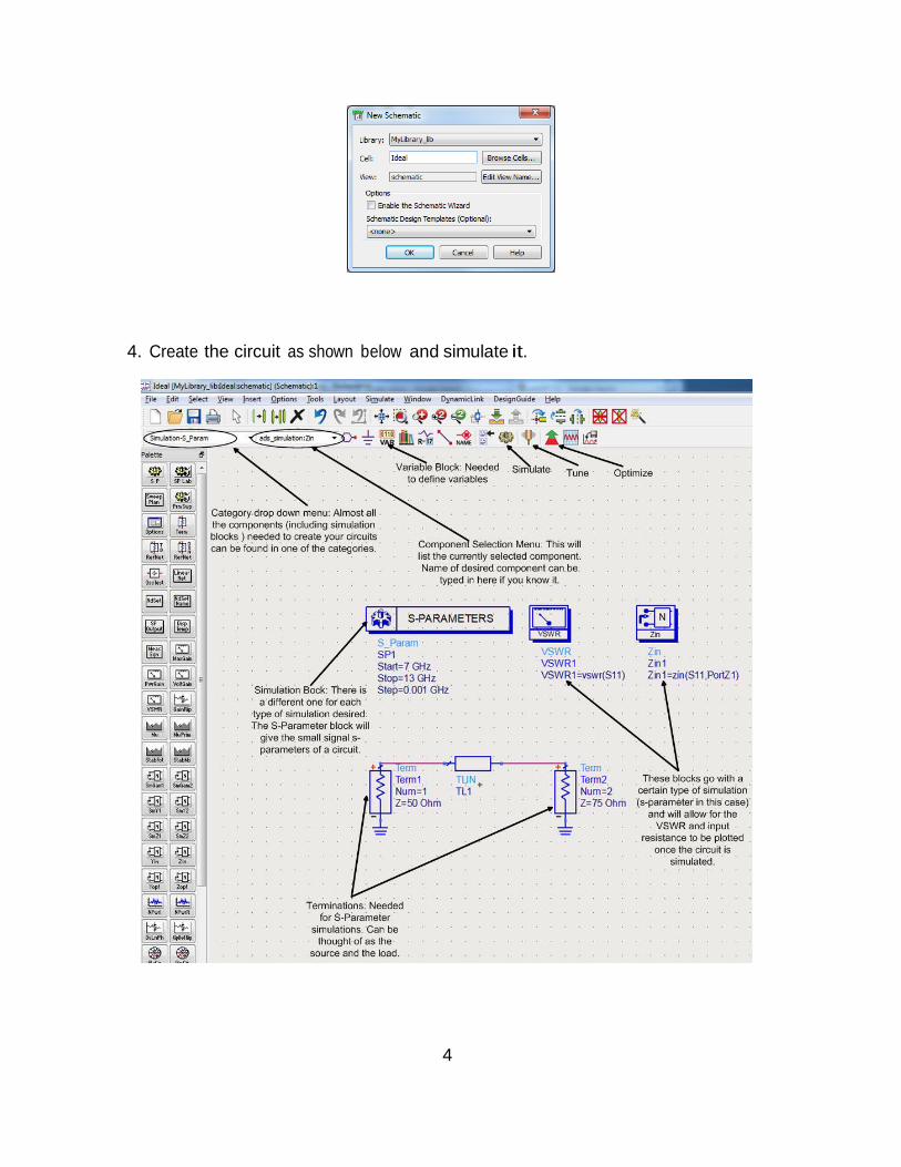
3. Make a new schematic in your project by going to File→New→Schematic and fill in
the window as shown below
4
4. Create the circuit as shown below and simulate it.
5
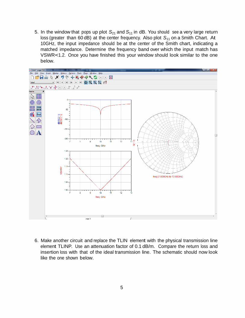
5. In the window that pops up plot S21 and S11 in dB. You should see a very large return loss (greater than 60 dB) at the center frequency. Also plot S11 on a Smith Chart. At 10GHz, the input impedance should be at the center of the Smith chart, indicating a matched impedance. Determine the frequency band over which the input match has VSWR<1.2. Once you have finished this your window should look similar to the one below.
6. Make another circuit and replace the TLIN element with the physical transmission line element TLINP. Use an attenuation factor of 0.1 dB/m. Compare the return loss and insertion loss with that of the ideal transmission line. The schematic should now look like the one shown below.
6
4 Microstrip Parameters
Use LineCalc (LineCalc can be found under tools on the menu bar) to determine the width of a 50Ω microstrip line, the width of a line having the required Z of the transformer section, and the width of a 75Ω microstrip line. Use Rogers RT/Duroid substrate with the following parameters:
• dielectric constant Er = 2.1
• dielectric loss tangent tanδ = 0.0001 at 10GHz
• substrate thickness h=31 mil (1 mil = 0.001 inch)
• copper conductor (σ = 5.8 × 10⁷)
7
• copper thickness 0.15 mil (weight 1/2 oz. per square foot)
• copper roughness 0.005 mil LineCalc should resemble that shown below.
Make a table for each microstrip line and enter the value of the attenuation constant and the phase constant, as each source of loss is considered (tand, imperfect conductor, conductor roughness), and when all losses are considered. What is the greatest contributor to the loss in each line?
5 Initial Microstrip Design
1. Enter the values for the substrate into the MSUB block found in the category drop down menu under tlines-microstrip.
2. Construct the circuit in ADS using microstrip components.
3. Simulate the circuit from 7-13 GHz. Plot the return loss(S11) and transmission loss
(S21) versus frequency. You should see a much lower return loss at the center frequency than the ideal design. What is the center frequency? Also look at the Smith Chart
8
display. At the center frequency, the input impedance should be near or at the center of the Smith Chart, indicting a matched impedance. What is the return loss and VSWR at the center frequency? Determine the frequency band over which the input match has VSWR<1.2. Compare your results to the ideal circuit first simulated. To get the input impedance and VSWR of the new circuit modify the old blocks to match the Term number used for the new circuit.
6 Include Microstrip Discontinuity Effects When the microstrip transmission line changes characteristic impedance, the width of the line changes abruptly. The abrupt change in physical width causes small reflections of the wave in the microstrip. In an equivalent circuit model, small shunt capacitance and small series inductance is added at the junction between the two different transmission lines. These reflections cause the center frequency of the design to be different than the original design.
1. Modify the microstrip design to include the impedance discontinuity effects. Use the
ADS circuit element MSTEP at the input and output of the quarter wave section. At this point labeling the pins is useful. Goto Options→Preferences, select the ’Pin/Tee’ tab and check the box ’Pin Numbers’.
2. Analyze your design from 7-13 GHz. Plot the return loss and transmission loss versus
frequency. You should see a slightly lower return loss at the center frequency than the microstrip design. What is the center frequency? Also look at the Smith Chart Display. At the center frequency, the input impedance should be near or at the center of the Smith Chart display. What is the return loss and VSWR at the center frequency? Compare the results of the last two simulations.
7 Tuning and Optimization The center frequency of the circuit that includes the effects of discontinuities has the center frequency slightly off 10GHz and needs to be retuned or optimized so that the desired performance is obtained. This can be done using tuning or optimization.
7.1 Tuning
1. Add a variable block to the schematic and add as variables the length and the width of the quarter-wave transformer line.
2. Make the variables tunable by clicking ’Tune/Opt/Stat/DOE Setup...’ when the vari-
able block is open. Select the Tuning tab and change ’tuning status’ to enabled. Set reasonable min, max, and step values. Do the same for the other variable.
9
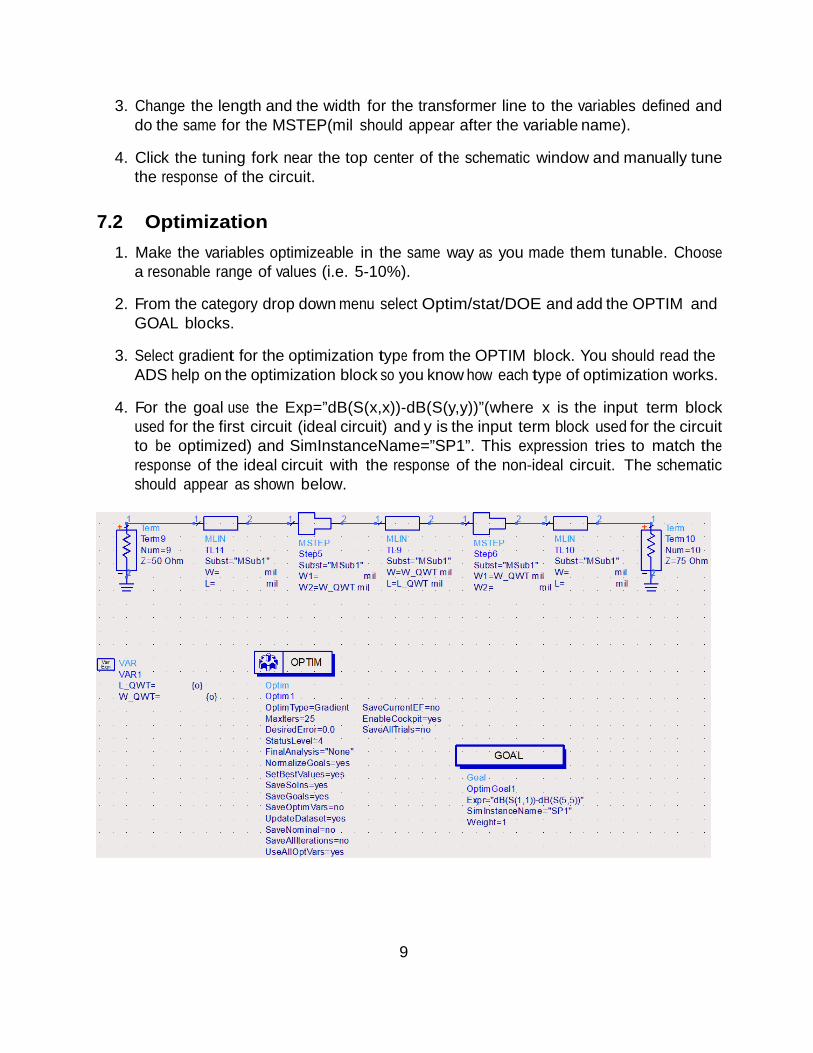
3. Change the length and the width for the transformer line to the variables defined and do the same for the MSTEP(mil should appear after the variable name).
4. Click the tuning fork near the top center of the schematic window and manually tune
the response of the circuit. 7.2 Optimization
1. Make the variables optimizeable in the same way as you made them tunable. Choose a resonable range of values (i.e. 5-10%).
2. From the category drop down menu select Optim/stat/DOE and add the OPTIM and
GOAL blocks.
3. Select gradient for the optimization type from the OPTIM block. You should read the ADS help on the optimization block so you know how each type of optimization works.
4. For the goal use the Exp=”dB(S(x,x))-dB(S(y,y))”(where x is the input term block
used for the first circuit (ideal circuit) and y is the input term block used for the circuit to be optimized) and SimInstanceName=”SP1”. This expression tries to match the response of the ideal circuit with the response of the non-ideal circuit. The schematic should appear as shown below.
10
5. Click the optimize shortcut button(beside the tuning fork).
6. What is the new length of the transformer section? What percentage change was nec- essary? Analyze your design from 7-13 GHz. Plot the return loss and the transmission loss versus frequency. What is the return loss and VSWR at the center frequency? Determine the frequency band over which the input match has a VSWR<1.2.
8 Circuit Board Layout Now ADS will be used to create a positive photomask of your final design. The CAD output file could be sent to a circuit board manufacturer to etch the top copper layer of the RT/Duroid circuit board (Circuit board consists of dielectric coated on both sides with copper). You should also add chevrons (100x100 mil) at the four corners to mark the outside edges of the circuit board and some identification. An example is shown below (not to scale). The dotted line shown the extent of the circuit board- do not put this line on the mask.
1. goto Layout→Generate/Update Layout...
2. A window should pop up. Select the input 50Ω line of the final circuit with the mouse.
The starting component should now be that line(This is so that only the last circuit constructed is generated in the layout). Click OK.
3. You should now see your quarter-wave transformer.
4. Add construction lines from Insert→Construction Line. This makes adding the chevrons
easier.
5. Make your layout so it resembles that shown below(layout not to scale).
11
9 Further Help Using Advanced Design System
If you are unsure on something in ADS the built-in help is extremely good. If you cannot find what you are looking for in the help munu try searching the web for a tutorial, design guide, or app note on it. Much of the information on the web will be for earlier versions of ADS, but this information should still be applicable for the current version. If you still cannot find what you are looking for ask another student in the class or email your TA.