46 IEEE JOURNAL OF RADIO FREQUENCY IDENTIFICATION, VOL. 5, NO. 1, MARCH 2021 Design of a Wide Planar Waveguide Antenna for UHF Near-Field RFID Reader With High Reading Rate Yusuke Ozawa, Qiang Chen , Senior Member, IEEE, Kunio Sawaya , Life Fellow, IEEE, Machiko Oouchida, and Masatomo Tokieda Abstract—UHF near-field RFID reader antenna based on leaky waveguide is proposed and the performance is evaluated using numerical simulation and experiment. In order to suppress the standing wave along transverse direction, a pair of notches is placed on the transverse edge of the mesh layer of the pla- nar waveguide. Diversity operation by switching impedance of the end terminal of the planar waveguide antenna is also intro- duced to suppress the standing wave effect along longitudinal direction. Numerical simulation and experiment show that the near-field null lines parallel to the longitudinal direction is almost removed by the presence of the notches and the distribution of the field strength becomes almost uniform because of the utiliza- tion of the switching diversity. It is demonstrated that the reading performance of the commercial RFID tags is greatly improved by using the proposed RFID reader antenna with the diversity operation of termination impedance. Index Terms—Planar waveguide antenna, reader antenna, UHF RFID, switching diversity. I. I NTRODUCTION A RADIO frequency identification (RFID) technology is capable of tracking and identifying items via communi- cations between RFID tags attached to the items and a reader antenna. Simultaneous detectability of RFID tags in non-line- of-sight environment is a significant advantage of the RFID technology over the conventional bar code systems which can only operate in line-of-sight environment [1]. Nowadays, most of the RFID systems work at four frequency bands: LF (125-134 kHz), HF (13.56 MHz), UHF (860-960 MHz) and microwave frequency (2.4 GHz and 5.8 GHz) bands. Among these frequency bands, UHF band is good at relatively wide reading range and high data-rate. The reading performance of RFID systems are sometimes degraded due to the effect of mutual coupling with surrounding scatterers [2], [3]. In order to solve this problem, near-field RFID system in UHF band has received broad attention [4] in the applications of item-level management such as so-called smart shelf system or conveyor Manuscript received May 27, 2020; revised September 10, 2020 and October 30, 2020; accepted November 3, 2020. Date of publica- tion November 23, 2020; date of current version February 20, 2021. (Corresponding author: Kunio Sawaya.) Yusuke Ozawa, Qiang Chen, and Kunio Sawaya are with the Department of Communications Engineering, Graduate School of Engineering, Tohoku University, Sendai 980-8579, Japan (e-mail: [email protected]). Machiko Oouchida and Masatomo Tokieda are with the Smart Sensing Business Development Project, Teijin Limited, Tokyo 100-8585, Japan. Digital Object Identifier 10.1109/JRFID.2020.3039016 system, where the RFID tags only in the vicinity of the reader antenna are detected [4]–[6]. Various reader antennas for UHF near-field RFID systems have been reported. In [7], a reader antenna based on the leaky wave microstrip line has been proposed. The detectable region can be controlled by changing the geometry of the microstrip line and the ground plane. The major disadvantage of the read- ing antenna was the low power efficiency due to the power absorption at the termination load of the leaky wave microstrip line. Therefore, relatively high power supplied to the reader antenna is required in order to activate IC chips embedded in RFID tags. In [8] and [9], array antennas focusing the near- field to a specific region were proposed. Detectable region of the array antennas can be switched flexibly, however, a compli- cated system composed of microwave components is required to switch the array antennas. A planar waveguide antenna having leaky waveguide struc- ture consisting of two conducting plates was developed [10]. Upper plate is a mesh plate while bottom one is a solid ground plane and they work as the parallel plate waveguide. The planar waveguide antenna transmits RF power to the RFID tags using evanescent wave on the mesh plate [11]. Detectable area of the planar waveguide antenna is limited to the area on the mesh plate because evanescent wave is localized only on the mesh plate. One of the problems of the planar waveg- uide antennas is how to alleviate the effect of standing wave, which yields null lines in the detectable region. Termination of the planar waveguide antenna with a matched load is one of the solutions, but it causes power loss at the terminated load [12]. In [13], multiple input ports were introduced to a planar waveguide in order to control its near-field distri- bution. The effect of the standing wave can be alleviated but the reader antenna becomes complicated and expensive. In our previous works, switching diversity technique was introduced to the planar waveguide antenna in order to switch the position of the null lines of standing wave parallel to the transverse direction [14]. The planar waveguide antenna is terminated by biased PIN diodes and the positions of the null lines are switched electrically. By switching terminal condition, the detectability can be improved without much power loss at the termination because the planar waveguide antenna is terminated by PIN diodes rather than the matched loads. When the width of planar waveguide antenna is less than a quarter wavelength, there is only the standing wave 2469-7281 c 2020 IEEE. Personal use is permitted, but republication/redistribution requires IEEE permission. See https://www.ieee.org/publications/rights/index.html for more information. Authorized licensed use limited to: TOHOKU UNIVERSITY. Downloaded on March 08,2021 at 02:44:58 UTC from IEEE Xplore. Restrictions apply.
Transcript
46 IEEE JOURNAL OF RADIO FREQUENCY IDENTIFICATION, VOL. 5, NO. 1, MARCH 2021
Design of a Wide Planar Waveguide Antennafor UHF Near-Field RFID Reader
With High Reading RateYusuke Ozawa, Qiang Chen , Senior Member, IEEE, Kunio Sawaya , Life Fellow, IEEE,
Machiko Oouchida, and Masatomo Tokieda
Abstract—UHF near-field RFID reader antenna based on leakywaveguide is proposed and the performance is evaluated usingnumerical simulation and experiment. In order to suppress thestanding wave along transverse direction, a pair of notches isplaced on the transverse edge of the mesh layer of the pla-nar waveguide. Diversity operation by switching impedance ofthe end terminal of the planar waveguide antenna is also intro-duced to suppress the standing wave effect along longitudinaldirection. Numerical simulation and experiment show that thenear-field null lines parallel to the longitudinal direction is almostremoved by the presence of the notches and the distribution ofthe field strength becomes almost uniform because of the utiliza-tion of the switching diversity. It is demonstrated that the readingperformance of the commercial RFID tags is greatly improvedby using the proposed RFID reader antenna with the diversityoperation of termination impedance.
Index Terms—Planar waveguide antenna, reader antenna,UHF RFID, switching diversity.
I. INTRODUCTION
ARADIO frequency identification (RFID) technology iscapable of tracking and identifying items via communi-
cations between RFID tags attached to the items and a readerantenna. Simultaneous detectability of RFID tags in non-line-of-sight environment is a significant advantage of the RFIDtechnology over the conventional bar code systems whichcan only operate in line-of-sight environment [1]. Nowadays,most of the RFID systems work at four frequency bands: LF(125-134 kHz), HF (13.56 MHz), UHF (860-960 MHz) andmicrowave frequency (2.4 GHz and 5.8 GHz) bands. Amongthese frequency bands, UHF band is good at relatively widereading range and high data-rate. The reading performance ofRFID systems are sometimes degraded due to the effect ofmutual coupling with surrounding scatterers [2], [3]. In orderto solve this problem, near-field RFID system in UHF band hasreceived broad attention [4] in the applications of item-levelmanagement such as so-called smart shelf system or conveyor
Manuscript received May 27, 2020; revised September 10, 2020and October 30, 2020; accepted November 3, 2020. Date of publica-tion November 23, 2020; date of current version February 20, 2021.(Corresponding author: Kunio Sawaya.)
Yusuke Ozawa, Qiang Chen, and Kunio Sawaya are with the Departmentof Communications Engineering, Graduate School of Engineering, TohokuUniversity, Sendai 980-8579, Japan (e-mail: [email protected]).
Machiko Oouchida and Masatomo Tokieda are with the Smart SensingBusiness Development Project, Teijin Limited, Tokyo 100-8585, Japan.
Digital Object Identifier 10.1109/JRFID.2020.3039016
system, where the RFID tags only in the vicinity of the readerantenna are detected [4]–[6].
Various reader antennas for UHF near-field RFID systemshave been reported. In [7], a reader antenna based on the leakywave microstrip line has been proposed. The detectable regioncan be controlled by changing the geometry of the microstripline and the ground plane. The major disadvantage of the read-ing antenna was the low power efficiency due to the powerabsorption at the termination load of the leaky wave microstripline. Therefore, relatively high power supplied to the readerantenna is required in order to activate IC chips embedded inRFID tags. In [8] and [9], array antennas focusing the near-field to a specific region were proposed. Detectable region ofthe array antennas can be switched flexibly, however, a compli-cated system composed of microwave components is requiredto switch the array antennas.
A planar waveguide antenna having leaky waveguide struc-ture consisting of two conducting plates was developed [10].Upper plate is a mesh plate while bottom one is a solid groundplane and they work as the parallel plate waveguide. Theplanar waveguide antenna transmits RF power to the RFIDtags using evanescent wave on the mesh plate [11]. Detectablearea of the planar waveguide antenna is limited to the area onthe mesh plate because evanescent wave is localized only onthe mesh plate. One of the problems of the planar waveg-uide antennas is how to alleviate the effect of standing wave,which yields null lines in the detectable region. Terminationof the planar waveguide antenna with a matched load is oneof the solutions, but it causes power loss at the terminatedload [12]. In [13], multiple input ports were introduced toa planar waveguide in order to control its near-field distri-bution. The effect of the standing wave can be alleviated butthe reader antenna becomes complicated and expensive.
In our previous works, switching diversity technique wasintroduced to the planar waveguide antenna in order to switchthe position of the null lines of standing wave parallel tothe transverse direction [14]. The planar waveguide antenna isterminated by biased PIN diodes and the positions of thenull lines are switched electrically. By switching terminalcondition, the detectability can be improved without muchpower loss at the termination because the planar waveguideantenna is terminated by PIN diodes rather than the matchedloads. When the width of planar waveguide antenna is lessthan a quarter wavelength, there is only the standing wave
OZAWA et al.: DESIGN OF WIDE PLANAR WAVEGUIDE ANTENNA FOR UHF NEAR-FIELD RFID READER WITH HIGH READING RATE 47
Fig. 1. Geometry of conventional planar waveguide antenna.
along the longitudinal direction and the field distribution alongtransverse direction is almost uniform.
In this article, a wide planar waveguide antenna for readerof UHF near-field RFID system is proposed, where there arestanding waves not only along the longitudinal direction butalso along the transverse direction. A pair of notches placedon the planar waveguide antenna is proposed in order to sup-press the standing wave current along the transverse direction.In addition, the switching diversity technique is introduced tothe proposed planar waveguide antenna which yields robustdetectability. Numerical simulation and experiment demon-strate the high detectability of the proposed antenna overconventional one. Finally, a prototype of the proposed pla-nar waveguide antenna for a smart book shelf system isdeveloped to demonstrate the advantage of the proposed planarwaveguide antenna with diversity operation.
II. PRINCIPLE OF PLANAR WAVEGUIDE ANTENNA
Figure 1 shows the geometry of conventional planarwaveguide antenna provided by Teijin Limited [10]. Thisantenna consists of three layers: a conducting mesh layer,a dielectric layer and a solid ground plane. Aluminum is usedfor the mesh layer and the ground plane. Relative permittivityof the dielectric layer is εr = 1.3. The antenna size is 800 mmin length, 326 mm in width and 2 mm in thickness. Theoperating frequency is 920 MHz, and thus the width is aboutone-wavelength. A part of the electromagnetic wave propagat-ing between the mesh layer and the ground plane leaks fromthe mesh apertures and attenuates exponentially as a functionof the distance z from the surface of the antenna. The rate ofthe decay of the electric field can be controlled by the size ofthe mesh apertures [9].
In order to show the basic characteristics of the pla-nar waveguide antenna and confirm the validity of theproposed antenna, numerical simulation using the method ofmoments (MoM) was performed. Since relative permittivityεr is close to unity and the MoM analysis including the
Fig. 2. Simulated current distribution on the mesh layer of conventionalplanar waveguide antenna.
effect of dielectric substrate requires time-consuming numeri-cal calculation, the dielectric layer is approximately modeledas vacuum.
Figure 2 shows the current distribution on the mesh layerobtained by the MoM analysis. Input power, which is the dif-ference between the incident power and the reflected power, isfixed to be 30 dBm in the simulation of the present paper. Itis shown that the current flows along not only longitudinal xdirection but also transverse y direction of the antenna becausethe width of the antenna is about one wavelength. Therefore,the near-field null lines occur parallel to both x direction andy direction above the antenna.
III. DESIGN AND SIMULATION OF PROPOSED ANTENNA
A. Antenna Geometry
Figure 3 shows the proposed antenna geometry schemati-cally. A pair of notches is placed on the mesh layer in order tosuppress the transverse current component. The open and shortcircuits obtained by switches shown in Figure 3 are used tomove the position of null lines parallel to transverse y directionand suppress the effect of the standing wave along longitudinalx direction [10].
B. Numerical Simulation
The performance of the proposed waveguide antenna wasevaluated by numerical simulation. Figure 4 shows the cur-rent distribution on the mesh layer of the antenna with openterminal. The notch position ds is set to be 110 mm where themagnitude of current |Iy| flowing along the edge of the feedingside (x = −400 mm) is maximum. The length of the notch Ls
is selected to be one-quarter of wavelength (= 81.5 mm) tosuppress the transverse electric current Iy along the edge. It isnoted that the magnitude of the transverse component of thecurrent |Iy| is suppressed by the presence of notches exceptfor the region of small x as shown in Figure 4 (b). It is also
Authorized licensed use limited to: TOHOKU UNIVERSITY. Downloaded on March 08,2021 at 02:44:58 UTC from IEEE Xplore. Restrictions apply.
48 IEEE JOURNAL OF RADIO FREQUENCY IDENTIFICATION, VOL. 5, NO. 1, MARCH 2021
Fig. 3. Geometry of proposed planar waveguide antenna.
Fig. 4. Current distribution on mesh layer of proposed antenna with openterminal (ds = 110 mm).
noted that the period of the standing wave along x decreasesas can be seen by comparison with the field distribution inFigure 2. By these observations, it is found that the directionof propagation of the electromagnetic wave traveling betweenthe mesh layer and the ground plane significantly changes bythe presence of the notches.
The effect of the notch position ds on the current distributionwas simulated and the results are shown in Figure 5, where theposition of the notch ds varies from 110 mm to 125 mm. It isshown that there is little change in the x-component of currenteven when the notch position ds changes. On the other hand,the y-component of the current reduces by 32 dB in the case ofds = 120 mm. Figure 6 shows the distribution of z componentof electric field with open terminal when the notch position ds
is 120 mm. It can be seen that the near-field null lines parallelto x direction are eliminated except for the region of small x.
Next, the effect of switching diversity was evaluated.Figure 7 shows the distribution of z component of electric
Fig. 5. Simulated current distribution on mesh layer of proposed antenna withvarying the position of notch ds.
Fig. 6. Simulated distribution of |Ez| in the horizontal plane (z = 30 mm)of the proposed antenna with open terminal.
field on the antenna with notches when the terminal conditionare open and short circuits. It can be seen that the standingwave occurring along longitudinal x direction varies dependingon the terminal condition. Therefore, the standing wave effectalong longitudinal direction can be reduced by the diversityoperation.
Finally, the electric field distribution in the horizontalplane for the case of the conventional antenna shown inFigure 1 is compared with that of the proposed antenna shownin Fig. 3 having notches with the diversity operation.Figure 8 shows the cumulative distribution function (CDF)of the strength of z component of electric field, where CDFis defined by the probability that the field strength |Ez| (V/m)is less than or equal to abscissa. In the case of discrete data,
Authorized licensed use limited to: TOHOKU UNIVERSITY. Downloaded on March 08,2021 at 02:44:58 UTC from IEEE Xplore. Restrictions apply.
OZAWA et al.: DESIGN OF WIDE PLANAR WAVEGUIDE ANTENNA FOR UHF NEAR-FIELD RFID READER WITH HIGH READING RATE 49
Fig. 7. Simulated distribution of |Ez| along y = 0 and z = 30 mm withvarying terminal condition.
Fig. 8. Cumulative distribution function of |Ez|.
CDF is the ratio of the number of measured points that the fieldstrength is less than or equal to the value of abscissa dividedby the total number of measured data. When the curve movesto right, field strength increases, and when the curve becomessteeper, the distribution of the field strength comes close tomore uniform distribution. In Figure 8, the electric field inthe vicinity of the feeding point is excluded considering thepractical use of the planar antenna. It is found that the CDFof the proposed antenna has steeper curve, which means thatthe electric field distribution is more uniform than the case ofthe conventional antenna.
IV. EXPERIMENTAL INVESTIGATION
The effect of the notches and switching diversity techniquewas investigated experimentally. Received power distributionon the planar waveguide antenna was measured by usingreceiving dipole antenna. Figure 9 shows the measurementsystem composed of a signal generator (Agilent E4438C),a spectrum analyzer (ROHDE/SCHWARZ FSU-26), dc powersupply (KENWOOD PW-36) for the bias of diodes and 3-axisscanner. Figure 10 shows a photo of experimental setup.Conducting plane was inserted to form a parallel plate waveg-uide in the vicinity of terminal region and switching diodeswere inserted at the terminal of the parallel plate waveguide as
Fig. 9. Experimental setup of near-field measurement.
Fig. 10. Photo of experimental setup of near-field measurement.
shown in Figure 9. The switching diodes used in this exper-iment are Toshiba 1SS352 and the number of diodes is 30.The distance between the lower end of the dipole antenna andplanar waveguide antenna is set to be 5 mm. The planar waveg-uide antenna is made by Teijin Limited and the size of theantenna is almost the same to the numerical analysis model.The notches are placed on the mesh layer and the length ofnotch Ls is 77 mm. The notch position ds is 90 mm. Theparameters of the measurement is listed in Table I. The valuesof Ls and ds in the experimental investigation are selected tobe slightly smaller than those in the numerical investigationin Section III, where the relative permittivity is assumed to beεr = 1.
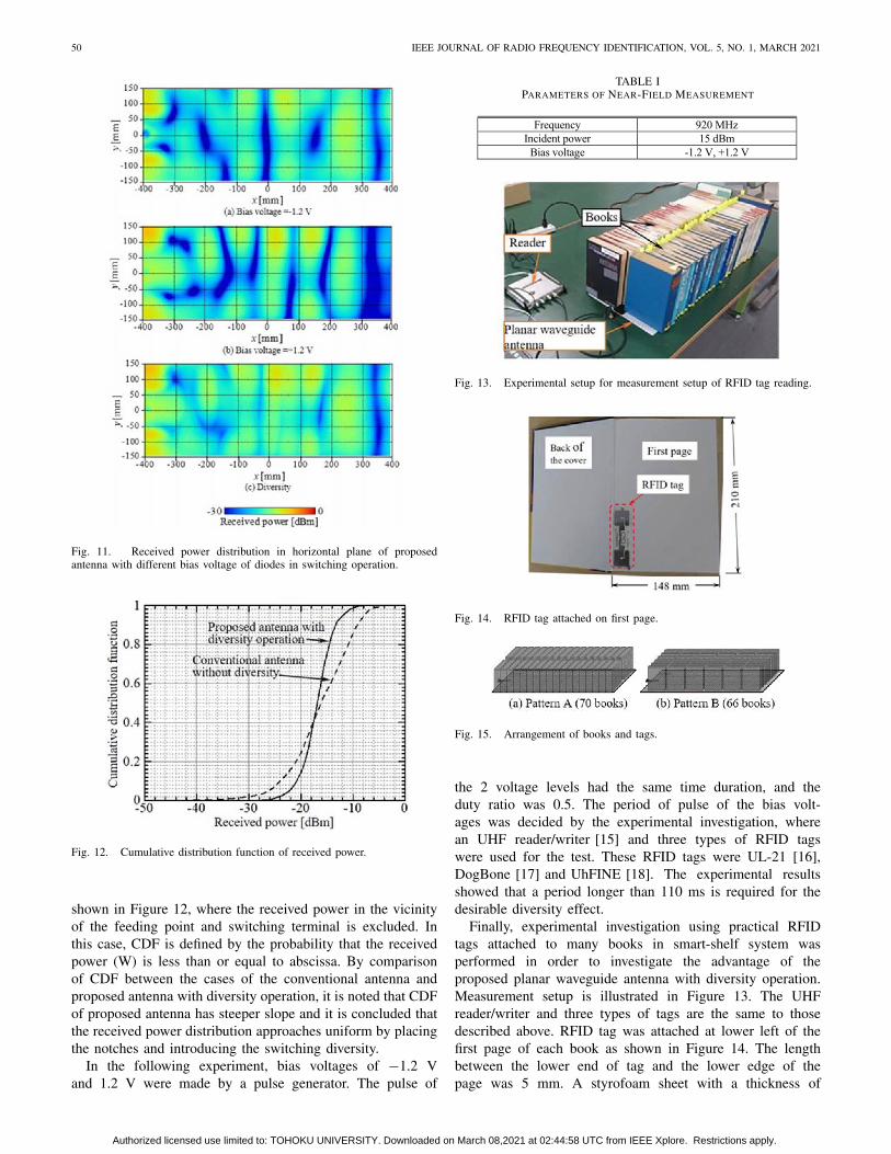
Figures 11 (a) and (b) show the measured power distribu-tion with varying the bias voltage of diodes in the switchingterminal. It can be seen that the standing wave occurring alongy direction is suppressed by the notches. It is also noted that theposition of standing wave along longitudinal direction x movesby changing the value of the bias voltage. Figure 11 (c) showsthe received power distribution when the switching diversityoperation is employed, where the larger value of the power ofFigures 11 (a) and (b) is plotted. It is shown that the near-fieldnulls parallel to longitudinal direction and transverse directionare almost removed. CDF of the received power distribution is
Authorized licensed use limited to: TOHOKU UNIVERSITY. Downloaded on March 08,2021 at 02:44:58 UTC from IEEE Xplore. Restrictions apply.
50 IEEE JOURNAL OF RADIO FREQUENCY IDENTIFICATION, VOL. 5, NO. 1, MARCH 2021
Fig. 11. Received power distribution in horizontal plane of proposedantenna with different bias voltage of diodes in switching operation.
Fig. 12. Cumulative distribution function of received power.
shown in Figure 12, where the received power in the vicinityof the feeding point and switching terminal is excluded. Inthis case, CDF is defined by the probability that the receivedpower (W) is less than or equal to abscissa. By comparisonof CDF between the cases of the conventional antenna andproposed antenna with diversity operation, it is noted that CDFof proposed antenna has steeper slope and it is concluded thatthe received power distribution approaches uniform by placingthe notches and introducing the switching diversity.
In the following experiment, bias voltages of −1.2 Vand 1.2 V were made by a pulse generator. The pulse of
TABLE IPARAMETERS OF NEAR-FIELD MEASUREMENT
Fig. 13. Experimental setup for measurement setup of RFID tag reading.
Fig. 14. RFID tag attached on first page.
Fig. 15. Arrangement of books and tags.
the 2 voltage levels had the same time duration, and theduty ratio was 0.5. The period of pulse of the bias volt-ages was decided by the experimental investigation, wherean UHF reader/writer [15] and three types of RFID tagswere used for the test. These RFID tags were UL-21 [16],DogBone [17] and UhFINE [18]. The experimental resultsshowed that a period longer than 110 ms is required for thedesirable diversity effect.
Finally, experimental investigation using practical RFIDtags attached to many books in smart-shelf system wasperformed in order to investigate the advantage of theproposed planar waveguide antenna with diversity operation.Measurement setup is illustrated in Figure 13. The UHFreader/writer and three types of tags are the same to thosedescribed above. RFID tag was attached at lower left of thefirst page of each book as shown in Figure 14. The lengthbetween the lower end of tag and the lower edge of thepage was 5 mm. A styrofoam sheet with a thickness of
Authorized licensed use limited to: TOHOKU UNIVERSITY. Downloaded on March 08,2021 at 02:44:58 UTC from IEEE Xplore. Restrictions apply.
OZAWA et al.: DESIGN OF WIDE PLANAR WAVEGUIDE ANTENNA FOR UHF NEAR-FIELD RFID READER WITH HIGH READING RATE 51
TABLE IIPARAMETERS OF TAG READING MEASUREMENT
TABLE IIIMEASUREMENT RESULTS OF READING RATE
5 mm was inserted on the planar antenna and the bookswith the RFID tag were placed on the styrofoam as shown inFigures 15 (a) and 15 (b). Parameters of the measurement isshown in Table II. Bias voltage of diodes was periodical squarewave at 2 Hz to accomplish the switching operation. The mea-surement was repeated ten times and the average reading rateof the RFID tags was evaluated.
Results of the measurement are shown in Table III. Thereading rate of the proposed antenna achieves over 93% forboth pattern A and pattern B, which is larger than the caseof conventional antenna. The reading rate is defined by theratio of the number of read tags for one reading cycle dividedby the total number of tags. Since there was a small ran-domness of electromagnetic field, the reading rate slightlychanged depending on the reading cycle, averaged readingrate over 10 cycles is shown Table III. The number of tagswhich cannot be read at all decreases by repeating the read-ing cycle. In many actual circumstances, all tags can be readby repeating several cycles when the reading rate is greaterthan 90%.
The detection performance of the RFID tags attached tobooks depends on the height of tags and it deteriorates as theheight increases. It also depends on the strength of multiplescattering waves produced by the surrounding objects. Theheight of the lower end of tag measured from the uppersurface of planar waveguide antenna is usually about 1 cmand desirable detection performance can be obtained. Thereceived voltage of the tag decreases as the height increases,however, detection performance is favorable even when theheight is 10 cm, provided the multiple scattering waves aresignificantly weak.
V. CONCLUSION
In this article, UHF near-field RFID reader antenna basedon leaky waveguide has been proposed and its performancewas evaluated using numerical simulation and experiment. Inorder to suppress the standing wave on the antenna alongtransverse direction, a pair of notches was placed on thetransverse edge of the mesh layer of the planar waveg-uide. Diversity operation by switching impedance of theterminal load of the planar waveguide antenna was intro-duced to suppress the standing wave effect along longitudinaldirection.
It has been shown by numerical simulation and experi-ment that the near-field nulls along the transverse direction
is almost removed by the presence of the notches of theproposed antenna and the distribution of the field strengthbecomes almost uniform by the use of the switching diver-sity. Moreover, it has been demonstrated that the read-ing performance of the commercial RFID tags attached tomany books for the proposed antenna with diversity isgreatly improved by comparison with that of the conventionalantenna.
Employment of the proposed methods in the reader anten-nas of practical RFID system may yield an indispensableincrease of the manufacturing costs, but the cost is accept-able when considering the significant improvement in readingperformance of the RFID system obtained by the proposedmethods.
REFERENCES
[1] K. Finkenzeller, RFID Handbook. Hoboken, NJ, USA: Wiley, 2010.[2] P. V. Nikitin and K. V. S. Rao, “Performance limitations of passive
UHF RFID systems,” in Proc. IEEE Antennas Propag. Soc. Int. Symp.,Oct. 2006, pp. 1011–1014.
[3] D. M. Dobkin and D. M. Weigand, “Environmental effects on RFIDtag antennas,” in Proc. IEEE MTT-S Int. Microw. Symp., Jun. 2005,pp. 135–138.
[4] P. V. Nikitin, K. V. S. Rao, and S. Lazar, “An overview of near fieldUHF RFID,” in Proc. IEEE Int. Conf. RFID, Mar. 2007, pp. 167–174.
[5] J. Shi, X. Qing, Z. N. Chen, and C. K. Goh, “Electrically large dual-loop antenna for UHF near-field RFID reader,” IEEE Trans. AntennasPropag., vol. 61, no. 3, pp. 1019–1025, Mar. 2013.
[6] Y. Yao, Y. Liang, J. Yu, and X. Chen, “Design of a multipolarized RFIDreader antenna for UHF near-field applications,” IEEE Trans. AntennasPropag., vol. 65, no. 7, pp. 3344–3351, Jul. 2017.
[7] C. R. Medeiros, J. R. Costa, and C. A. Fernandes, “RFID reader anten-nas for tag detection in self-confined volumes at UHF,” IEEE AntennasPropag. Mag., vol. 53, no. 2, pp. 39–50, Apr. 2011.
[8] H.-T. Chou, C.-T. Yu, K.-T. Wang, and P. Nepa, “A simple design ofpatch antenna array with an optimized field distribution in the near-zonefor RFID applications,” IEEE Antennas Wireless Propag. Lett., vol. 13,pp. 257–260, Feb. 2014.
[9] W. Choi, J. S. Kim, G. Choi, and J. S. Chae, “Near-field antenna forRFID smart shelf in UHF,” in Proc. IEEE Antennas Propag. Soc. Int.Symp. USNC/URSI Nat. Radio Sci. Meeting (APSURSI), Jun. 2009,pp. 1280–1283.
[10] Teijin Limited. Accessed: Mar. 7, 2014. [Online]. Available: https://www.teijin.com/news/2014/ebd140307_11.html
[11] H. Shinoda, Y. Makino, N. Yamahira, and H. Itai, “Surface sensornetwork using inductive signal transmission layer,” in Proc. Int. Conf.Netw. Sensing Syst. (INSS), Jun. 2007, pp. 201–206.
[12] A. O. Lim, K. Tezuka, and B. Zhang, “An experiment study of elec-tromagnetic field distribution over 2D communication system,” in Proc.Asia Pac. Microw. Conf. (APMC), Dec. 2009, pp. 1266–1269.
[13] T. Kagawa, T. Matsuda, B. Zhang, and Y. Kado, “Power provisionscheme considering shadowing effect for two-dimensional communica-tion systems,” in Proc. Asia Pac. Conf. Commun. (APCC), Aug. 2013,pp. 525–530.
[14] K. H. Chen, Q. Chen, K. Sawaya, M. Oouchida, and Y. Hirano,“Diversity reception of 920 MHz RFID reader antenna in smart-shelfsystem,” in Proc. Int. Symp. Antennas Propag. (ISAP), Nov. 2015,pp. 851–853.
Authorized licensed use limited to: TOHOKU UNIVERSITY. Downloaded on March 08,2021 at 02:44:58 UTC from IEEE Xplore. Restrictions apply.
52 IEEE JOURNAL OF RADIO FREQUENCY IDENTIFICATION, VOL. 5, NO. 1, MARCH 2021
Yusuke Ozawa received the Graduation degreefrom the Faculty of Engineering, Tohoku University,Sendai, Japan, in 2016, and the M.E. degree inthe subject of communications engineering fromGraduate School, Tohoku University in 2018. Duringhis M.E. study, he performed research on the UHFRFID reader antenna.
Qiang Chen (Senior Member, IEEE) receivedthe B.E. degree from Xidian University, Xi’an,China, in 1986, and the M.E. and D.E. degreesfrom Tohoku University, Sendai, Japan, in 1991and 1994, respectively, where he is currently aChair Professor of Electromagnetic EngineeringLaboratory with the Department of CommunicationsEngineering, Faculty of Engineering. His primaryresearch interests include antennas, microwave andmillimeter wave, electromagnetic measurement, andcomputational electromagnetics. He received the
Best Paper Award and the Zen-ichi Kiyasu Award in 2009, from theInstitute of Electronics, Information and Communication Engineers (IEICE).He served as the Chair of IEICE Technical Committee on Photonics-AppliedElectromagnetic Measurement from 2012 to 2014, the Chair of IEICETechnical Committee on Wireless Power Transfer from 2016 to 2018, andthe Chair of IEEE Antennas and Propagation Society Japan Chapter from2017 to 2018. He is currently the Chair of IEICE Technical Committee onAntennas and Propagation, and a Fellow of IEICE.
Kunio Sawaya (Life Fellow, IEEE) receivedthe B.E., M.E., and Ph.D. degrees from TohokuUniversity, Sendai, Japan, in 1971, 1973, and 1976,respectively, where he was a Research Associate,an Associate Professor, and a Professor withthe Department of Electrical and CommunicationEngineering from 1976 to 2013. He is a ProfessorEmeritus with Tohoku University. He was alsoa Specially Appointed Professor of the PromotionOffice with Strategic Innovation, Tohoku Universityfrom 2015 to 2019. His areas of interests are anten-
nas in plasma, antennas for mobile communications, theory of scattering anddiffraction, antennas for plasma heating, and array antennas. He received thePaper Awards in 1988 and 2009, the Communications Society Paper Awards in2006 and 2014, and the Zen-ichi Kiyasu Award in 2009 all from the Instituteof Electronics, Information and Communication Engineers (IEICE). He servedas the Chair of the Technical Group with Antennas and Propagation of IEICEfrom 2001 to 2003, the Chair of the Organizing and Steering Committees of2004 International Symposium on Antennas and Propagation (ISAP’04), thePresident of the Communications Society of IEICE from 2009 to 2010, andthe Chair of IEEE Sendai Section from 2012 to 2013. He is a Fellow and anHonorary Member of IEICE.
Machiko Oouchida received the B.E. and M.E.degrees from Hiroshima University, Higashi-Hiroshima, Japan, in 2004 and 2006, respectively.She joined Teijin Limited, where she is currentlywith Technology Development Team, the SmartSensing Business Development Project.
Masatomo Tokieda received the B.E. degree fromOita University in 1995, and the M.E. degree fromKumamoto University, Kumamoto, Japan, in 1997.In 2016, he joined Teijin Limited, where he is cur-rently a Product Manager with the Smart SensingBusiness Development Project.
Authorized licensed use limited to: TOHOKU UNIVERSITY. Downloaded on March 08,2021 at 02:44:58 UTC from IEEE Xplore. Restrictions apply.


![Planar Microstrip-To-Waveguide Transition in Millimeter-Wave Band · 2013-03-12 · that of ordinary transitions of a waveguide and a coaxial cable [11]. The probe transition connects](https://static.documents.pub/doc/80x56/5e930936dfd03a310714bb10/planar-microstrip-to-waveguide-transition-in-millimeter-wave-band-2013-03-12-that.jpg)


![Reconfigurable Modular Antenna for Near-Field UHF RFID ... · NF UHF RFID systems, typically based on microstrip [13]-[15], Coplanar Stripline (CPS) [16] or Coplanar Waveguide (CPW)](https://static.documents.pub/doc/80x56/5f44c6435989354d992b9139/reconfigurable-modular-antenna-for-near-field-uhf-rfid-nf-uhf-rfid-systems.jpg)


![INVITED PAPER Planar Waveguide Arrays for Millimeter Wave ...€¦ · [10]–[13]. Four types of planar waveguides, all belong-ing to single-layer waveguide, are structurally quite](https://static.documents.pub/doc/80x56/5f0780907e708231d41d4cb3/invited-paper-planar-waveguide-arrays-for-millimeter-wave-10a13-four.jpg)
