Page 1
Design of CMOS Sigma-Delta modulators for audio applications
M.Sc. Thesis authored by: Shen Qifeng Supervisors: Erik Bruun Pietro Andreani
Ørsted•DTU Center for Physical Electronics Technical University of Denmark Bldg. 349 DK-2800 Kgs. Lyngby Denmark http://www.oersted.dtu.dk/ Tel: (+45) 45 25 39 06 Fax: (+45) 45 81 01 17
Date:
15 July 2007
Classification:
Public
Issue:
1st edition
Notes:
This thesis has been submitted to the Technical University of Denmark in partial fulfilment of the requirements for the M.Sc. degree. The thesis represents 30 ECTS point.
Copyright:
© Shen Qifeng, 2007
Page 3
Abstract
Sigma-delta ADC, not only has adopted the technology of oversampling, but also utilized
noise shaping which modulate the quantization noise in the baseband to the high
frequency area. It increases the SNR in baseband and the effective quantization number
of the converter. Because of the modulation technology, it makes sigma-delta ADC
allowed to use one bit comparator, in addition Conventional Nyquist converters require
analog components that are precise and highly immune to noise and interference while
Sigma-delta converters can be implemented using simple and high-tolerance analog
components. Currently, sigma-delta ADCs have been widely used for audio A/D
conversion.
In this thesis, the principles of sigma-delta ADCs are discussed firstly. Then the 16
bits audio sigma-delta ADC has been designed using the top-down design method.
The architecture and design methods of sigma-delta modulators are studied. Based on
it, the bits of quantizer, oversampling ratio and the orders and topology of modulator
have been analyzed and designed. Then a stable 3rd order single loop modulator has been
implemented. This novel architecture is more insensitive to the performance of analog
circuit and the matching of component. At the same time the influence of various
non-ideal factors also has be considered.
1
Page 4
The proposed modulator has been designed with fully differential switched capacitor
circuit. And the ways to optimize the circuit architecture, minimize the circuit
non-idealities and improve the circuit performance are analyzed combined with the
characteristics of the modulator architecture. Based on it, the switched capacitor
integrator, operational amplifier, non-overlap clock, comparator, feedback DAC have
been designed.
2
Page 5
Acknowledgements
At first I would like to thank Professor Erik Bruun and Professor Pietro Andreani, for
their advice and suggestion on this thesis, and efforts and contribution on the course of
31630 Integrated Analog Electronics and 31636 CMOS RF Integrated Circuits, in which
I learned much knowledge about analog and RF IC design.
Thanks also to my parents and my girlfriend, for their always supporting me, encouraging
me and loving me.
Finally, I would like to express my gratitude to DTU for giving me this opportunity to
purse my master degree in this beautiful and fantastic county.
3
Page 7
TABLE OF CONTENTS
1. Introduction……………………………………………………………………………7
1.1 Background……………………………………………………………………………...7
1.2 Research object………………………………………………………………………...11
1.3 Thesis organization……………………………………………………………………12
2. Overview of sigma-delta modulator………………………………...…13
2.1 Oversampling principle……………………………………………………………....13
2.2 Basic sigma-delta modulator principle……………………………………………..16
2.2.1 First order sigma-delta modulator……………………………………………16
2.2.2 Second order sigma-delta modulator………………………………………...20
2.2.3 High order sigma-delta modulator……………………………………………21
2.3 Advance sigma-delta modulator principle………………………………………….22
2.3.1 Cascaded sigma-delta modulator……………………………………………..22
2.3.2 Multi-Bit Quantization…………………………………………………………23
2.3.3 Continuous time modulator……………………………………………………24
2.3.4 Idle tones issues………………………………. ………………………………..25
2.3.5 Stability issues………………………………. …………………………………26
3. System level design of sigma-delta modulator..............................28
3.1 Architecture choice analysis…………………………………………….................28
5
Page 8
3.2 Coefficients of Modulator……………………………………. …………………..32
3.3 Non-idealities analysis………………………………. …………………………….43
4. Circuit level design of sigma-delta modulator………………..54
4.1 Switched capacitor integrator………………………………………………….….55
4.2 Capacitors………………………………. ………………………………. …………59
4.3 Operational amplifier……………………………………………………………….60
4.4 Comparator………………………………. ………………………………………….70
4.5 Clock phase generation………………………………. ……………………………73
4.6 1 bit DAC………………………………. …………………………………………...75
4.7 Conclusion………………………………. …………………………………………..76
5. Conclusion…………………………………………………………………………...78
6
Page 9
Chapter 1
Introduction
1.1 Background
A signal is an object, a symbol, a sound, a gesture, used to represent a piece of
information [1]. Signals have been used since prehistory. Electricity has only been used
as a vehicle for information interchange since the first half of the 19th Century. When
Morse developed the telegraph,its use of a discrete set of symbols makes the telegraph
the first digital system in the history of electrical engineering. The invention of the
transistor and the microprocessor has helped making the digital processing of data faster
and cheaper than ever. With the development of application specific integrated circuits
and specified processors, more and more people tend to favor digital processing signals
as opposed to the corresponding analog processing.
The advantage of digital processing is obvious [2]. Digital signals are much more
immune to noise than their analog counterparts. Noise and distortion will accumulate
during the transfer or copy of an analog signal, while a digital signal can be lossless
copied or transferred as long as the noise and distortion are lower than the threshold
which changes the digital value. Moreover, signal processing circuits can be implemented
7
Page 10
more easily, accurately and economically in digital domain thanks to the fast and
continuous development of CMOS process.
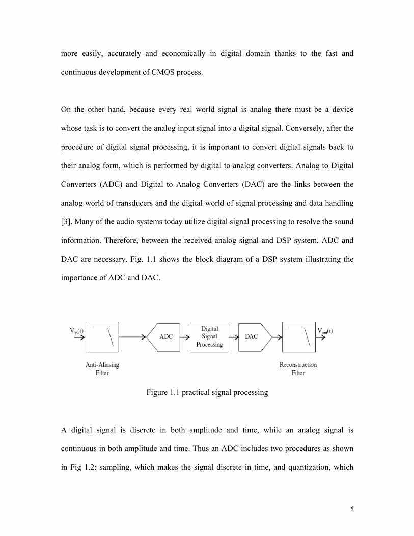
On the other hand, because every real world signal is analog there must be a device
whose task is to convert the analog input signal into a digital signal. Conversely, after the
procedure of digital signal processing, it is important to convert digital signals back to
their analog form, which is performed by digital to analog converters. Analog to Digital
Converters (ADC) and Digital to Analog Converters (DAC) are the links between the
analog world of transducers and the digital world of signal processing and data handling
[3]. Many of the audio systems today utilize digital signal processing to resolve the sound
information. Therefore, between the received analog signal and DSP system, ADC and
DAC are necessary. Fig. 1.1 shows the block diagram of a DSP system illustrating the
importance of ADC and DAC.
Figure 1.1 practical signal processing
A digital signal is discrete in both amplitude and time, while an analog signal is
continuous in both amplitude and time. Thus an ADC includes two procedures as shown
in Fig 1.2: sampling, which makes the signal discrete in time, and quantization, which
8
Page 11
makes the signal discrete in amplitude. Accordingly there are two important
specifications for an ADC: speed and resolution. The speed represents how fast the
discrimination in time can be done. The resolution represents how accurate the
discrimination in amplitude can be done. Effective Number of Bit is often used to
characterize the conversion resolution.
Figure 1.2 Analog to Digital Conversion
According to Shannon’s sampling theorem [4], a band-limited analog signal must be
sampled at least twice of its highest frequency component so that the signal can be
reconstructed without loss. Many ADCs are designed to sample the signal just a little
faster than the Nyquist frequency. These ADCs can be categorized as Nyquist-rate ADCs
[5]. They can operate at very high speed, resulting in a large bandwidth. Using a standard
CMOS process, the conversion bandwidth is expanded to the range of Giga Hz. The main
drawback of Nyquist-rate ADCs is their low resolution, which is limited by the matching
of analog components. Practically 12~14 bit resolution can be achieved using
Nyquist-rate ADCs. Another problem is the complex hardware structure. For a flash
structure ADC, the hardware complexity exponentially increases with the resolution.
Using other structures like pipeline or folding can reduce the required number of
9
Page 12
comparators, which is however still large.
On the other hand, sigma-delta ADCs provide a robust and economical solution for
high-resolution ADC [6]. Sigma-delta modulator is one kind of the so-called error
feedback coder, meaning that the coarse quantization error is feedback to the input. A
sigma-delta modulator arranges the loop filter in a way that the input signal and the
quantization error by different transfer functions. The quantization error goes through a
first order or higher order difference, yet the input signal is simply delayed. Theoretically
the conversion resolution can be arbitrarily increased until the physical limitation of
device thermal noise floor is reached. The high resolution is achieved through a feedback
loop from the digitized output to the modulator input. Since there is a large gain in the
forward path of the loop, the long-term average of the digitized output is forced to be
very close to the modulator input.
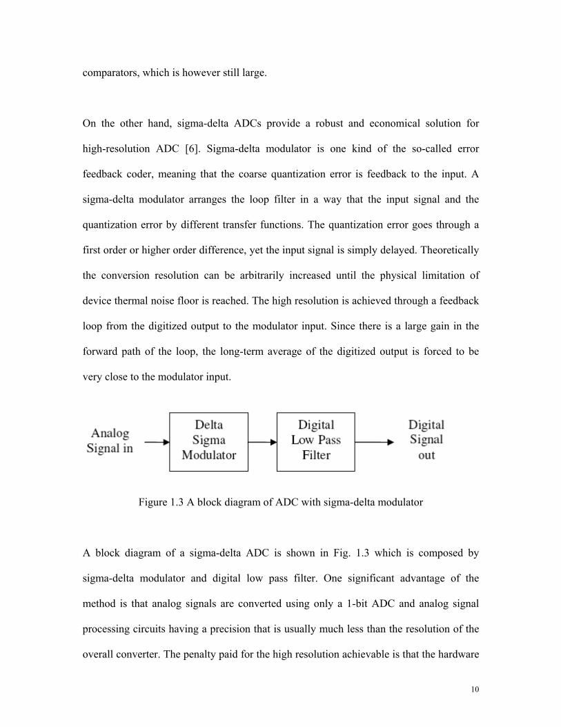
Figure 1.3 A block diagram of ADC with sigma-delta modulator
A block diagram of a sigma-delta ADC is shown in Fig. 1.3 which is composed by
sigma-delta modulator and digital low pass filter. One significant advantage of the
method is that analog signals are converted using only a 1-bit ADC and analog signal
processing circuits having a precision that is usually much less than the resolution of the
overall converter. The penalty paid for the high resolution achievable is that the hardware
10
Page 13
has to operate at the oversampling rate, much larger than the maximum signal bandwidth,
thus demanding great complexity of the digital circuitry. Because of this limitation, these
converters have traditionally been relegated to high-resolution, low frequency
applications. To further improve the conversion resolution at the same sampling speed,
noise shaping can be applied. This is accomplished by high-pass filtering the quantization
noise to push most of its power from signal frequencies higher frequencies. The
decimation filter that follows the quantizer then removes the quantization noise appearing
at the frequencies greater than base-band to improve the effective resolution of the
converter.
1.2 Research Objective
In recent years sigma-delta modulator has become the focus of analogue to digital
converter field, particular in low frequency and audio applications [7]. The objective of
this thesis is to design a 16 bit sigma-delta modulator for audio frequency application.
Frequencies up to 20 kHz and oversampling ratio 128 is implemented by using TSMC
0.35μm technology. A complete design analysis and simulation will be presented form
system level to circuit level.
11
Page 14
1.3 Thesis organization
This thesis is divided into five chapters. Chapter 2 will briefly discuss the fundamentals
of sigma-delta modulators. Chapter 3 will consider and determine the proper architecture
and orders of modulator as well as comparator level and oversampling ratio, moreover
detail coefficients analysis and simulation also will be presented, associated with the
main non-idealities that affect the performance of proposed sigma-delta modulators.
Chapter 4 will describe the implementation of proposed sigma-delta modulator with
transistor level circuit as well as analyze and simulate core components in the modulator.
Finally, in chapter 5 a summary and conclusions of this work will be presented and some
suggestions regarding the future work that can be pursued also will be discussed.
12
Page 15
Chapter 2
Overview of sigma-delta modulator
This chapter overviews different kinds of sigma-delta converters. They can be separated
to two categories, which are single loop and multi loop cascaded sigma-delta ADCs. The
basic operation of the sigma-delta A/D converters is first introduced. Then, high order
and multi-loop sigma-delta converters are discussed. Finally, multi-bit and continuous
time modulator also will be mentioned.
2.1 oversampling principle
Digital signal processing relies on discrete samples of data. According to the Nyquist
theorem, the sampling frequency, fs, has to be at least twice as large as the bandwidth of
the input signal, fB, to obtain an unambiguous reproduction of the signal. If this theorem
is not fulfilled, aliasing will occur and information is lost. Data converters using fs = fNy =
2fB are hence called Nyquist converters. However, for reasons of noise margin and filter
design complexity, a sampling speed of fs > fNy is usually applied.
The process of quantization can be modeled a process where the output y(n) is
determined from the input sample x(n) plus an additive noise component e(n) as shown in
Fig. 2.1.
13
Page 16
To further simplify the analysis of the noise from the quantizer, the following
assumptions about the noise process and its statistics are traditionally made,
1. The error sequence e(n) is a sample sequence of a stationary random process.
2. The error sequence is uncorrelated with the sequence x(n).
3. The random variables of the error process are uncorrelated; i.e. the error is a
white-noise process.
4. The probability distribution of the error process is uniform over the range of
quantization error.
Power Pe is derived to equal △2/12 [2], where corresponds to the quantization step △
size. Therefore, the spectral density of the quantization noise, Se(f) is constant for a
certain .△
Figure 2.1 quantization model
Sampling at a frequency much higher than the Nyquist rate is called oversampling and
14
Page 17
the rate by which fs exceeds fNy is called the oversampling ratio, OSR
2s s
Ny B
f fOSRf f
= = (2.1)
Due to the white noise assumption, a larger sampling frequency causes the constant
quantization noise power to be distributed over a larger spectrum. This reduces the noise
power in the band of interest. A filter that limits the band to fB cuts off all noise
components for f > fB reducing the remaining quantization noise power, Pe0, within DC
and fB. It can be shown that the quantization noise power is decrease by a factor OSR.
2 1(12eP
OSRΔ
= ) (2.2)
Figure 2.2 Quantization noise power spectral density for Nyquist rate and oversampled
rate
Therefore, each doubling of the sampling frequency decreases the in-band noise by 3 dB
and thus increases the resolution by half a bit. Fig. 2.2 shows the power spectral density
of the quantization noise for Nyquist rate sampling and oversampling rate. For Nyquist
rate Sampling, all the quantization noise power, represented by the area of the tall shaded
rectangle, occurs across the signal bandwidth. In the oversampled case, the same noise
15
Page 18
power, represented by the area of the unshaded rectangle has been spread over a
bandwidth equal to the sampling frequency, which is much greater than the signal
bandwidth, fB. Only a relatively small fraction of the total noise power falls in the band
[-fB,fB], and the noise power outside the signal band can be greatly attenuated with a
digital low-pass filter following the ADC.
2.2 sigma-delta modulator principle
2.2.1 First order sigma-delta modulator
Sigma-delta modulator’s name is derived from the difference and summing nodes in a
loop conFiguration. Additional to oversampling, sigma-delta modulators modify the
spectral properties of the quantization noise. They are said to shape the noise spectral
density, Se(f), such that it is low in the band of interest and high elsewhere [23] . This
spectral shaping results from a negative feedback loop system as shown in Fig. 2.3. Here,
the linear quantizer model from Fig. 2.1 is employed.
Figure 2.3 prototype of sigma-delta modulator
16
Page 19
Signal input x (n) and quantization noise contribution e(n) are assumed to be independent,
leading to an examination using the superposition principle. With the help of the
z-transform, the output is described as
( ) ( ) ( ) ( ) ( )TF TFY z S z X z N z E z= + (2.3)
Where Signal Transfer Function (STF) and Noise Transfer Function (NTF) can be
derived as
( ) ( )( )( ) 1 ( )TF
Y z H zS zX z H
= =+ z
(2.4)
( ) 1( )( ) 1 ( )TF
Y zN zE z H z
= =+
(2.5)
H(z) denominates a generic filter function.
In order to minimize the effect of quantization noise at the output, the NTF(z) should
reach its minimum in the band of interest. That is achieved when H(z) reaches its
maximum. However, STF(z) would be close to unity for a maximum of H(z), leaving the
input signal almost unchanged. There are many transfer functions that satisfy this
condition and could be used to implement a noise shaping modulator, but one class of
transfer functions comprised of integrators is especially suited for VLSI implementation
because the analog circuits required to implement the transfer function are simple and
robust. A z-domain representation of this class sigma-delta modulator is shown in Fig.
2.4. The modulator is comprised of a subtraction node, a discrete-time integrator, and a
1-bit quantizer.
17
Page 20
Figure 2.4, 1st order sigma-delta modulator with discrete time integrator
First order noise shaping can be obtained by choosing the pole of H(z) to be located at
DC. A straightforward integrator satisfies this requirement having
1( )1
H zz
=−
(2.6)
With equation (2.6), the signal transfer functions becomes a simple delay
11/( 1)( )1 1/( 1)TF
zS z zz
−−=
+ −= (2.7)
Whereas the noise transfer function describes a high-pass filter function
11( ) (1 )1 1/( 1)TFN z z
z−= =
+ −− (2.8)
The quantization noise power for first order noise shaping, Pe, is approximated in the
band of interest with
2 2 2 2302 1( )( )( ) ( )
12 3 36es
fP 3
f OSRπ πΔ Δ
= = (2.9)
18
Page 21
And the maximum SNR for this modulator is given by
2max 2
3 310( ) 10 log( 2 ) 10 log( ( ) )2
Ns
e
PSNR OSRP π
= = + 3 (2.10)
Or equivalently,
max 6.02 1.76 5.17 30log( )SNR N OSR= + − + (2.11)
These relationships show that the resolution of the first order sigma-delta modulator
increase with OSR at a ratio of 1.5 bit per octave. Although an improvement of 1 bit in
SNR is observed in the first order sigma-delta modulator when compared with the
performance of an ADC using only oversampling, the required fs could still being very
high for certain applications.
Figure 2.5 Comparison between oversampling with and without noise shaping
Our discussion of sigma-delta conversion to this point has been from a linearized
frequency domain standpoint, now we look at these converter operation from the time
19
Page 22
domain. Because we have oversampled our input signal, its value changes very slowly
compared to the sampling frequency. Referring to Fig. 2.3, except for the case when the
input x[n] exactly equals one of the binary values of the quantizer, a tracking error comes
about e[n]=x[n]-y[n]. The integrator in the forward path accumulates this error over time
and the quantizer simply feeds back a value that will minimize this accumulated error
such that the long term average of this tracking error is zero. Thus, y[n] can be viewed as
a rapidly changing approximation to our input signal that has an average value equal to
x(n).
2.2.2 Second order sigma-delta modulator
The architecture of a second order modulator is shown in Fig. 2.6. As it is seen, it
comprises two integrators, and the analysis of this modulator can be treated in the same
way as with the previous one. The single bit quantizer can be substituted with an additive
white noise source as it is depicted in Fig. 2.1 and after that, finding out an expression for
the output in the z-domain.
Figure 2.6 2nd order sigma-delta modulator with discrete time integrators
Performing the mentioned steps leads to the following equation
20
Page 23
1( )TFS f z−= (2.12)
1 2( ) (1 )TFN f z−= − (2.13)
As the same way described above, the maximum SNR for this modulator is given by
max 6.02 1.76 12.9 50log( )SNR N OSR= + − + (2.14)
Equations 2.14 show that for a second order modulator the SNR and increase at a ratio of
2.5 bit per octave of OSR. From Equation 2.14 it can be observed that double the order of
a sigma-delta modulator reduces the required OSR by given SNR. This intuitively leads
to the supposition that using high order loops is the way to have high SNR with moderate
fs. In the next section a brief analysis and discussion of a high order high order
sigma-delta modulator is presented.
2.2.3 High order sigma-delta modulator
A conceptual architecture of n-order sigma-delta modulator that produces a quantization
noise differencing of order n is presented in Fig 2.7. The single bit quantizer introduces
the quantization noise and could also be substituted by the linear stochastic model of Fig
2.1. It can be demonstrated that the output of such a system equals to:
1( ) ( ) ( )(1 )nY z X z z E z z−= + − 1− (2.15)
And the the maximum SNR for n-order modulator is given by
2max 2
3 310( ) 10 log( 2 ) 10 log( ( ) )2
Ns
e
PSNR OSRP π
= = + 3 (2.16)
21
Page 24
Figure 2.7 high order sigma-delta modulator with discrete time integrators
2.3 Advance sigma-delta modulator principle
2.3.1 Cascaded sigma-delta modulator
Sigma-delta architectures may be classified as either single-loop or cascaded, which
consist of a cascade of single loop sigma-delta modulators.
Cascaded employ 2 or more modulator loops, each comprising a low order modulator to
maintain stability. Each following loop processes only the quantization noise of the
previous loop, which improves the total resolution. The quantization noise of the
following loops is subtracted from the output of the first loop in digital error cancellation
logic, further reducing the total quantization noise. The arrangement for realizing a
second order modulator using two first order modulators is shown in Fig. 2.8.
22
Page 25
Figure 2.8 Cascaded sigma-delta modulator
2.3.2 Multi-Bit Quantization
Another option for improving the signal to noise ratio at low oversampling ratios is to
extend the single bit quantization into multiple bits. The main difference between a
multi-bit and a single-bit architecture is that single-bit architectures have a 2-level
quantizer, while multi-bit architectures have a quantizer with M-levels where M > 2. The
main quality of sigma-delta modulators employing multi-bit quantizers is that the SNR is
dramatically improved. In comparison with a single-bit modulator, a multi-bit structure
typically provides an increase of 6 dB per additional bit. Therefore, it is possible to
increase the overall resolution of any sigma-delta ADC without increasing the OSR by
simply increasing the number of levels in the internal quantizers. Equivalently,
23
Page 26
architectures with multi-bit quantizers can achieve resolutions comparable to those of
architectures with single-bit quantizers at lower OSR. Furthermore the use of multi-bit
quantization improves stability in high-order modulators [11].
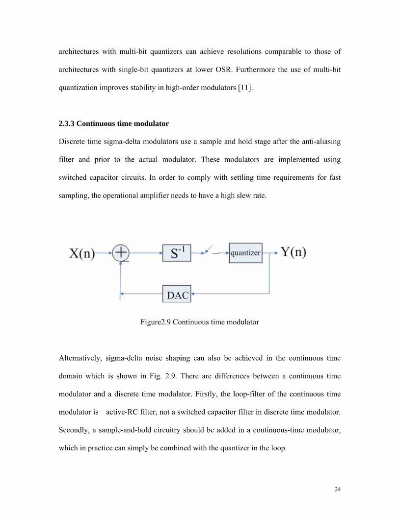
2.3.3 Continuous time modulator
Discrete time sigma-delta modulators use a sample and hold stage after the anti-aliasing
filter and prior to the actual modulator. These modulators are implemented using
switched capacitor circuits. In order to comply with settling time requirements for fast
sampling, the operational amplifier needs to have a high slew rate.
Figure2.9 Continuous time modulator
Alternatively, sigma-delta noise shaping can also be achieved in the continuous time
domain which is shown in Fig. 2.9. There are differences between a continuous time
modulator and a discrete time modulator. Firstly, the loop-filter of the continuous time
modulator is active-RC filter, not a switched capacitor filter in discrete time modulator.
Secondly, a sample-and-hold circuitry should be added in a continuous-time modulator,
which in practice can simply be combined with the quantizer in the loop.
24
Page 27
2.3.4 Idle tones issues
Thus far, the only source of converter error that we have looked at is that due to
quantization. However, there is another source of error named as idle tones. Even when
utilizing ideal analog components, low-order 1-bit noise shaping loops are prone to this
error which is oscillatory in nature. It is brought about by certain DC inputs that cause the
quantization error to be deterministic. For these certain inputs, the binary quantizer output
y[n] will exhibit a long and complex pattern. When the period of this sequence is long
enough, its fundamental component lies in the band of our signal of interest and will not
be attenuated by the decimator and thus SNR is degraded.
Consider the case of applying a DC level 1/3 to input of 1st order sigma-delta modulator,
the output will be y(n)={1,1,-1,1,1,-1,1,1……..}, This sequence has its power at DC and
fs/3. The fs component will be filtered by the low-pass filter leaving us with only a DC
component.
Now let us consider a DC input level of (1/3+1/24)=3/8 to our modulator. This yields a
quantizer output sequence y(n)={1,1,-1,1,1,-1,1,1,-1,1,1,-1,1,1,1,-1,1,1,-1….}, We see
that this output sequence has its power at DC and at fs/16. If our converter's OSR is
equal to 8, then the low-pass filter will not eliminate the signal's power at fs/16 and we
will get a tone in our output spectrum in addition to the DC component.
25
Page 28
2.3.5 Stability issues
The most obvious drawback of high order single loop modulator is the stability problem.
In order to illustrate it clearly, we use 3rd order single loop modulator as example. From
equation 2.15, the transfer function of 3rd order single loop modulator can be described as
3 1 3
( ) ( ) ( ) ( ) ( )
( ) (1 ) ( )TF TFY z S z X z N z E z
X z z z E z− −
= +
= + − (2.17)
From that, we can find that this system have three poles at origin and three zeros at z=1.
However, this system is probably unstable and the reason is that equation 2.17 is derived
from the assumption
( ) ( ) ( )Y z Q z E z= + (2.18)
Where Q(z) is input of quantizer and E(z) is additive noise, and they are unrelated. In the
case of one bit quantizer, this assumption is failed since the output of one bit quantizer is
determined by the polarity of input and whatever value of input, the amplitude output is
always equal to one, thus this process should be described by non-linear models.
( ) ( ) ( )Y z KQ z E z= + (2.19)
Where K is the variable gain of one bit quantizer, and the variable range is from zero to
one. Therefore the new transfer function changes to
3
3( )(1 )( 1)
KzSTF zKz K z
=+ − − 3 (2.20)
3
3
( 1)( )(1 )( 1)zNTF z
Kz K z−
=+ − − 3 (2.21)
26
Page 29
The system polarities can be derived from
3 (1 )( 1) 0Kz K z+ − − =3 (2.22)
For stability, all roots must be within the unit circle, while when 0<K<0.5, there are two
polarities outside the unit circle, which means K should larger than 0.5.
Moreover, since the output amplitude of quantizer is fixed, a small K means larger input
signal, confirming the observation that instability an be prevented by limiting the input
signal.
27
Page 30
Chapter 3
System level design of sigma-delta modulator
In this chapter the system level design of the proposed sigma-delta modulator is
presented as well as analysis of non-idealities in practical implementation. System level
design is a very important task that should be carried out in an iterative manner if there is
an interest in achieving an optimal solution. System level design is assisted by behavioral
simulation and these kinds of simulations are helpful to verify whether the developed
system satisfies the imposed requirements.
The discussion here starts with the set of specifications derived in the chapter 2. After
that, the most important architectural choice can be found, analyzed and their suitability
for a reconFigurable solution compared. After that architectural analysis, the adopted
solution is presented and the design of the NTF and STF that fulfill the requirements as
well as the stability criteria is carried out. At last, practical non-idealities in the modulator
will be analyzed and simulated.
3.1 Architecture choice analysis
Continual time modulator or discrete time modulator
The first choice that must be made in designing sigma-delta modulator is a selection
28
Page 31
between a discrete time implementation and continuous time implementation [22]. The
primary difference is that discrete time systems employ switched capacitor integrators
while continuous-time systems use active-RC integrators in the modulators. There are a
number of advantages and disadvantages associated with each option. Switched capacitor
integrators take advantage of VLSI capabilities by eliminating the need for physical
resistors. On-chip resistors with very high linearity are difficult to achieve in a standard
CMOS process. In addition, resistors in continuous time integrators need to be kept small
to minimize thermal noise. For the same time constant, reducing the resistors implies that
the capacitors need to be increased. This may make the area large and the capacitors
impractical to realize on-chip.
The frequency response of switched capacitor integrators can be more accurately
predicted because the time-constant is a function of capacitor ratios and of the sampling
frequency. The time-constant of continuous-time integrators, on the other hand, relies on
absolute component values rather than capacitor ratios, the impact of process and
temperature variations is worse than for a switched capacitor implementation. The
absolute value of on-chip poly resistors typically vary far from the desired value, whereas
capacitor ratios are usually better controlled.
Another advantage of switched capacitor systems is that they are less sensitive to clock
jitter and the op-amp settles. As long as the op-amp settles to the required accuracy, it
does not matter whether the op-amp slews or linearly settles. Continuous-time integrators,
however, must be linear at all times. On the other hand Continuous-time systems also
29
Page 32
have some advantages. Because the op-amp in an active-RC integrator does not have to
settle to full accuracy every half clock period, a very high oversampling ratio is
achievable. The oversampling ratio in switched capacitor integrators is limited by the
achievable bandwidths of the op-amp. This makes continuous time modulators very
appealing for high-speed applications [24]. Moreover, continuous time systems eliminate
the need for an anti-alias filter prior to the sigma-delta ADC. The elimination of this filter
results in significant power savings for the receiver. To conclude in this thesis the
switched capacitor implement is selected due to the requirement of high resolution and
low frequency.
Qutiziter bits
In principle, multi bit architectures allow reaching high SNR for low OSR. The stability
is much easier to achieve since low order loops can still being used for a more spread
range of SNR. Even in high order loops, stability is improved because the finer
quantization error requires lower signal swing in the operational amplifiers. However, the
advantages of multiple bit quantizers cannot be completely obtained because the linearity
requirements imposed to the internal DAC are very severe. Any distortion or DC offset
introduced by the DAC adds directly to the signal path without shaping and degrading so
the performance of the whole converter. Dynamic element matching techniques can
reduce these effects, but at the expense of more circuitry and power consumption.
On the other hand, single bit high order sigma-delta modulators become very attractive
because they are able to reach high values of SNR for modest OSR and their circuit
30
Page 33
implementation is very robust. Single bit modulators have the highest linearity of all
architectures and simplify a lot the design of the DAC embedded in the feedback path.
Oversampling rate
As described in chapter 2, it is known that in the case of same order of sigma-delta
modulator, the higher OSR, the easier to realize larger dynamic range and high revolution.
However, in practice it is difficult to implement higher OSR because it increases the
difficulty of analog circuit design, specially with lager band width and slew rate of
operational amplifier. In addition, it consumes more power of circuit.
Therefore, for the audio signal with bandwidth of 20~20KHz, it is proper to choose 64 or
128 OSR to achieve optimal organization of architecture and OSR. In this design, OSR is
equal to 128 and N frequency is 48KHz by leaving some margin, thus sampling
frequency is 6.144MHz.
Loop architecture of modulator
Another determination should be made is to choose the proper loop architecture. As
described in chapter 2, in order to design stable high order sigma-delta modulators, it
consists in connecting low order sections in cascade, obtaining the desired high order
modulator. Since first and second order noise shaping loops are unconditionally stable,
the entire system shows also the same stability property.
In order to make choice between high order single loop architecture and cascade loop
31
Page 34
architecture, since analog imperfections such as leakage or gain errors present in the
implementation of the elements comprised by the integrated circuits while cascade
modulator requires perfect matching among integrators which is difficult to design in
sub-micrometric technologies and is so more sensitive to operational amplifier
non-idealities than corresponding single loop modulators. So that the most convenient
architectural option is offered by the single bit high order loop. They have the least
overhead for the circuit realization of the quantizer and A/D converter in both circuit area
and power consumption. They also have the interesting characteristic of synthesizing
different types of NTF by changing the filter coefficients, which in turn are passive
components, without altering the modulator structure, leaving the active circuit elements
ready for their reemployment.
According to equation 2.16 in charter 2, it is readily to calculate the peak SNR of 1st , 2nd
and 3rd sigma-delta modulator.
1
2
3
66100133
SNR dBSNR dBSNR dB
≈⎧⎪ ≈⎨⎪ ≈⎩
( 3.1)
With the requirement of 16 bit audio ADC, it should have 98dB SNR at least, thus it is
impossible for 1st as well as 2nd modulator although the later can provide 100dB SNR.
However, if it takes non-ideality of practical circuit into account, 2dB margin is
insufficient. Therefore 3rd order modulator is a candidate in this design.
3.2 Coefficients of Modulator
32
Page 35
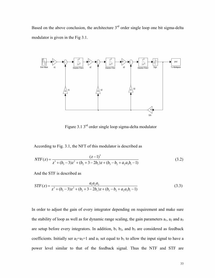
Based on the above conclusion, the architecture 3rd order single loop one bit sigma-delta
modulator is given in the Fig 3.1.
-K- b3-K- b2-K- b1
-K-
a3
-K-
a2
-K-
a1
yout
To WorkspaceSine Wave Sign
z -1
1-z -1
Discrete Filter2
z -1
1-z -1
Discrete Filter1
z -1
1-z -1
Discrete Filter
-K-
D/A
Figure 3.1 3rd order single loop sigma-delta modulator
According to Fig. 3.1, the NFT of this modulator is described as
3
3 23 2 3 3 2 2 3 1
( 1)( )( 3) ( 3 2 ) ( 1
zNTF zz b z b b z b b a a b
−=
+ − + + − + − + − ) (3.2)
And the STF is described as
1 2 33 2
3 2 3 3 2 2 3 1
( )( 3) ( 3 2 ) ( 1
a a aSTF zz b z b b z b b a a b
=+ − + + − + − + − )
(3.3)
In order to adjust the gain of every integrator depending on requirement and make sure
the stability of loop as well as for dynamic range scaling, the gain parameters a1, a2 and a3
are setup before every integrators. In addition, b1 b2, and b3 are considered as feedback
coefficients. Initially ser a2=a3=1 and a1 set equal to b1 to allow the input signal to have a
power level similar to that of the feedback signal. Thus the NTF and STF are
33
Page 36
reconFigured as
3
3 23 2 3 3 2 1
( 1)( )( 3) ( 3 2 ) ( 1
zNTF zz b z b b z b b b
−=
+ − + + − + − + − ) (3.4)
13 2
3 2 3 3 2 1
( )( 3) ( 3 2 ) ( 1
bSTF zz b z b b z b b b
=+ − + + − + − + − )
(3.5)
It should be mentioned that designing proper architecture of modulator is as same as
choosing the right NTF with high-pass filter ability, to shape the quantization noise away
from DC to high frequency domain. Moreover, we wish to make the NTF as large as
possible outside the frequency band of interest. However, in order to guarantee the
stability, NTF(z) should be less than 6 dB, and for the high order sigma-delta modulator,
this value is best less than 3.5dB.
Figure 3.2 Frequency response of IIR filters
34
Page 37
Fig. 3.2 shows that the frequency response of the Butterworth filter is maximally flat in
the passband, and rolls off towards zero in the stopband, when compared to Chebyshev
filter or Elliptic filter. Thus Butterworth filter is the proper candidate for sigma-delta
modulator design. This kind of filter can be described as
3
3 2 2( )2 2
c
c c
H ss s s
ω3
cω ω ω=
+ + + (3.6)
With the help of Matlab, this Butterworth filter with passband edge at 390 kHz has the
best balance between large dynamic input range and high SNR.
Thus such a high-pass filter can be obtained when the poles are placed in a Butterworth
conFiguration, and the NTF has the following form
3
3 2
( 1)( )2.2071 1.6992 0.4479
zNTF zz z z
−=
− + − (3.7)
Compared to equation 3.4, the following description can be obtained
3
2 3
3 2 1
3 2.20713 2 1.6992
1 0.4497
bb bb b b
− = −⎧⎪ + − =⎨⎪ − + − = −⎩
(3.8)
Finally the gain and feedback coefficients can be obtained
1
2
3
1
2
3
0.0442110.04420.2850.7929
aaabbb
=⎧⎪ =⎪⎪ =⎪⎨ =⎪⎪ =⎪
=⎪⎩
(3.9)
By simulation of matlab [16],the pole-zero distribution is shown in Fig. 3.3 and
frequency response of STF and NTF is shown in Fig 3.4.
35
Page 38
Figure 3.3 Pole-zero distribution of NTF
0 0.05 0.1 0.15 0.2 0.25 0.3 0.35 0.4 0.45 0.5-350
-300
-250
-200
-150
-100
-50
0
50
STF NTF
Figure 3.4 frequency response of STF and NTF
36
Page 39
-120 -110 -100 -90 -80 -70 -60 -50 -40 -30 -20 -10 00
10
20
30
40
50
60
70
80
90
100
110
120
Input level, dB
SN
R c
urve
X: -3Y: 113
Figure 3.5 SNR versus input power of proposed sigma-delta modulator
101 102 103 104 105 106 107-250
-200
-150
-100
-50
0
Figure 3.6 PSD of proposed sigma-delta modulator
37
Page 40
Fig. 3.5 shows the measured SNR as a function of input power, from which we can
Figure out the max input is -3dB and the corresponding max SNR is 113dB. The PSD
result of modulator is shown in the Fig 3.6 with the normalized input 0.7.
Meanwhile, in order to watch the every output of integrators, we add scopes at the points
of each output, which is shown in Fig. 3.7.
-K- b3-K- b2-K- b1
-K-
a3
-K-
a2
-K-
a1
yout
To WorkspaceSine Wave Sign
Scope3Scope2Scope1Scope
z -1
1-z -1
Discrete Filter2
z -1
1-z -1
Discrete Filter1
z -1
1-z -1
Discrete Filter
-K-
D/A
Figure 3.7 3rd order single loop sigma-delta modulator with scopes
Figure 3.8 output of first integrator
38
Page 41
Figure 3.9 output of second integrator
Figure 3.10 output of third integrator
It should be noticed that each output of integrators are Fig. 3.8 3.9 and 3.10, which show
that the outputs are 0.382, 1.3379 and 2.55 respectively, so that it is necessary to perform
dynamic-range scaling to ensure that all nodes have approximately the same power level
and there will be no unnecessarily large noise gain from nodes with small signal levels.
39
Page 42
Note that for the reason of illustration simply, we use input one here so that DAC is
normalized to 1/0.7=1.42. To increase the output level of a node by a factor k, the input
branch of this node should be multiplied by k while the output branches should be
divided by k.
1 0.0442 / 0.382 0.15171 0.0442 / 0.382 0.1517
ab
= =⎧⎨ = =⎩
(3.10)
Thus perform the same procedure to calculate other coefficients and finally the following
values can be obtained
1
2
3
1
2
3
0.15170.28550.52470.15170.21300.3109
aaabbb
=⎧⎪ =⎪⎪ =⎪⎨ =⎪⎪ =⎪
=⎪⎩
(3.11)
By simulating in the matlab with new coefficients, the corresponding results are shown
below
Figure 3.11 output of first integrator after scaling
40
Page 43
Figure 3.12 output of second integrator after scaling
Figure 3.13 output of third integrator after scaling
41
Page 44
101 102 103 104 105 106 107-250
-200
-150
-100
-50
0
Figure 3.14 PSD of proposed sigma-delta modulator after signal scaling
And it should be noticed that the value of each output of integrators is around 1V as well
as the whole system is stable. The ideal SNR is 110.6dB.
42
Page 45
3.3 non-idealities analysis
The non-idealities of modulator in practical implementation can be categorized in 3
classes [17][26][27].
(1) Clock jitter
(2) Integrator related noises
(3) Operational amplifier related non-idealities, such as finite gain, bandwidth and
slew-rate.
Clock jitter
Clock jitter is caused by thermal noise or phase noise in every clock generation circuits.
Once the analog signal has been sampled, variations of the clock period have no direct
effects on the circuit performance, which means the effect of clock jitter on circuit can be
described by the influenced sampling of the input signal.
Clock jitter can be defined as a short-term variation of the switching instant of a digital
clock from its theoretical position, which results in a non-uniform sampling time
sequencely, and produce an error increasing the total error power at the quantizer output.
When a sinusoidal input signal x(t) with amplitude A and frequency f is sampled at an
instant, while the error t is given by△
( )( ) ( ) 2 cos(2 ) dx tx t t x t f ft t tdt
π π+ Δ − = Δ = Δ (3.12)
43
Page 46
This error can be modeled at the behavioral level by using the model shown in Fig. 3.15
1Out1
Zero-OrderHold1
Zero-OrderHold
RandomNumber
Product
k
Gain
du/dt
Derivative
Add
1In1
Figure 3.15 Modeling a random sampling jitter
The continuous-time input signal x(t) and the jitter are summed together and then the
output are sampled with sampling period Ts by a zero-order hold. The random noise
comes from a random block creating a sequence of random numbers with Gaussian
distribution, zero mean and unity standard deviation.
Noise
The most significant noise sources in the integrators are the thermal noise associated to
the sampling switches and the intrinsic noise of operational amplifier. These noises are
only taken into account in the first integrator since the noises of other stages of
integrators are suppressed and shaped due to the nature of the sigma-delta modulator.
(1) Switched thermal noise
Switched thermal noise is generated by the switches due to the random thermal energy
motion and it is present even at equilibrium[24].
44
Page 47
The total noise power of the integrator can be calculated by evaluating as following
20
41 (2 )
ontot
on s s
kTR kTP dffR C Cπ
∞
=+∫ = (3.13)
Where k is the Boltzmann’s constant, T is the absolute temperature, and 4kTRon is the
noise PSD associated with the switch on-resistance.
The switched thermal noise voltage eT(n) appears as an additive noise to the input voltage
x(t), which leads to
( ) [ ( ) ( )] [ ( ) ( )] [ ( ) ( )]Ts f
kT kTy t x t e t b x t n t b x t n t bC bC
= + = + = + (3.14)
Where n(t) denotes a Gaussian random process with unity standard deviation, and b is the
integrator gain. The behavior model is shown in Fig. 3.16.
1Out1
Zero-OrderHold
RandomNumber
Product1
Product
f()
Function-CallGenerator
Add
2In2
1In1
Figure 3.16 modeling switches thermal noise
However, this type of noise is significant at the first input integrator, because the white
45
Page 48
noise in the subsequent integrator will be noise shaped by high-pass filters. Another issue
of switched thermal noise is integrator may include more than one input branch and each
contributes to the total noise power. In this model, there are two branches that one is input
sampling branch and the other one is modeled by the feedback from the modulator
output.
(2) Op-amp noise
The noise source in the operational amplifier generally consists of a thermal part and a
flicker part. For a MOSFET operating in strong inversion region, the thermal noise can be
modeled by a current source in parallel with the channel. The mean-square value of the
input-referred thermal noise within the bandwidth Δf of a MOSFET in saturation is
approximately
2,
24 ( )3n in
m
V kTg
= fΔ (3.15)
The flicker (or 1/f) noise, which is nearly independent of the bias condition, is
approximated by
2,n f
ox
KVC WL f
Δ=
f (3.16)
where k is a process and temperature dependent parameter. Flicker noise dominates at
low frequencies and decreases with the increase of frequencies. The frequency at which
1/f noise is equal to the white thermal noise is called corner frequency fcr. Beyond fcr,
thermal noise dominates. The flicker (1/f) noise and wide-band op-amp thermal noise are
46
Page 49
uncorrelated in the same device, so their noise powers can be directly added together.
Practically they can be obtained from circuit simulation, calculation and measurement
during the integration phase, by adding the noise contributions of all the devices referred
to the op-amp input and integrating the resulting value over the whole frequency
spectrum. If assuming that the total rms noise voltage referred to the op-amp input is Vn,
the behavior model of the effect of the op-amp noise on Sigma-delta modulators can be
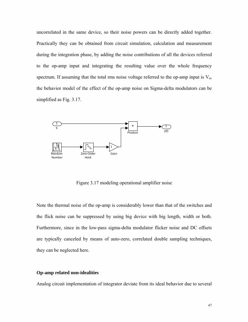
simplified as Fig. 3.17.
1y(t)
Zero-OrderHold
RandomNumber
Product
1
Gain
1b
Figure 3.17 modeling operational amplifier noise
Note the thermal noise of the op-amp is considerably lower than that of the switches and
the flick noise can be suppressed by using big device with big length, width or both.
Furthermore, since in the low-pass sigma-delta modulator flicker noise and DC offsets
are typically canceled by means of auto-zero, correlated double sampling techniques,
they can be neglected here.
Op-amp related non-idealities
Analog circuit implementation of integrator deviate from its ideal behavior due to several
47
Page 50
non-ideal effects including integrator’s finite DC gain and bandwidth, slew rate limiting
and saturation voltage, which are the consequence of practical operational amplifier.
These non-ideal factors will be considered in the following.
(1) DC gain
The transfer function of an ideal integrator with unity coefficient is
1
1( )1
zH zz
−
−=−
(3.17)
The DC gain of the integrator described by Equation 3.17 is infinite. However, the actual
gain is limited by circuit constraints and in particular by the operational amplifier
open-loop gains A0. The integrator leakage caused by finite-DC-gain of the op-amp in the
integrator can be modeled with a variable. the parameter α is approximated with
0
0
f
f s s
A C
RA C C Cα =
+ + (3.18)
The transfer function of the integrator with leakage becomes
1
1( )1
zH zzα
−
−=−
(3.19)
Therefore, the pole location is shifted. It can be modeled in Simulink as illustrated in Fig.
3.18
48
Page 51
1Out1z
1
Unit Delay Saturation
1
Gain
Add
1In1
Figure 3.18 modeling finite DC gain
Considering the integrator leakage, specifically, when α approximates to 1. For the
reason of simplicity, in 1st-order loop, the STF and NTF of the modulator are given,
respectively:
1
11
1
1
( ) 1( )( ) 1
1
zY z zSTF z z
zX zz
α
α
−
−−
−
−
−= = ≅+
−
(3.20)
11
1
( ) 1( ) (1 ) (1 )( ) 1
1
Y zNTF z z zzE z
z
α 1
α
− −−
−
= = ≅ − + −+
−
(3.21)
Note from Equation 3.20 that the leakage affects the signal transfer function introducing a
gain error that, in general, will be negligible. On the other hand, the leakage (1-α) shifts
the zero location away from its ideal position at z=1 in the noise-shaping function. Note
that the first term corresponds to the ideal 1st-order shaping, whereas the leakage adds a
second term that is not shaped.
49
Page 52
(2) BW and SR
Linear settling and slew rate specify the small signal and large signal speed performance
of an integrator respectively. As the clock frequency increases in Sigma-delta
modulators to process wideband signals, integrator defective settling becomes one of the
bottlenecks in present switched capacitor designs. The output voltage settling error is
basically caused by the finite gain-bandwidth and slew-rate of the amplifiers, which are
the two distinct parts of the setting behavior of amplifier. In the slow rate region, the
output of the amplifier operates in the nonlinear part, while in the small signal period it
behaves linearly. In the high frequency application, if amplifier operates in fast regime
where the steeling time constant is large and slew rate is smaller than a low limit, the
settling behavior will be affected nonlinearly, which ultimately destroyed performance of
sigma-delta modulator.
Since slew rate appearing or not depends on the instantaneous amplitude of the input
signal, the relationship between slew rate and the level of the input signal will be studied
as follows.
In a switched capacitor integrator, the input signal consists of the assumed sinusoidal
input signal minus the feedback signal and the evolution of the output node during nth
integration period is given by
0 0( ) ( ) (1 )t
ss s s
I
Cv t v nT T V eC
τ−
= − + − (3.22)
Where Vs=Vin(nTs-Ts/2), and τ=1/(2piGBW) is the time constant of the integrator and
50
Page 53
GBW is the unity gain frequency of the integrator loop-gain during the considered clock
phase.
The maximum slope value of this curve is:
0 max( ) | s s
I
C Vd v tdt C τ
= (3.23)
Regarding to the settling error, two separated cases have been considered: linear, partial
slew. The value specified by 3.23 is lower than the operational amplifier SR (taking into
account all of the capacitors connected to the operational amplifier output during the
considered clock phase). There is no slew-rate limitation, and the integrator output will
be linearly settled.
The value specified by 3.23 is larger than SR. In this case, the operational amplifier is in
slewing
(3.24) 0 0 0( ) ( )s st t v t v nT t SRt≤ = − +
0
0 0 0 0 0( ) ( ) ( ) (1 )t t
ss
I
Ct t v t v t v SRt eC
τ−
−> = + − × − (3.25)
Where 0svt
SRα τ= −
The integrator can be described in the MATLAB function block as shown in Fig.3.19.
51
Page 54
1Out1z
1
Unit Delay Saturation
MATLABFunction
MATLAB FcnAdd
1In1
Figure 3.19 modeling slew rate function
In the case of the linear settling, the incomplete settling causes a degradation of the
integrator gain; in the case of the nonlinear settling, the incomplete settling causes a
nonlinear gain, since the gain of the integrator is dependent on the input.
kT/C
IN
kT/C noise3
kT/C
IN
kT/C noise2
1/8
OpNoise
White noise1
yout
To Workspace
Switch Non-Linearity1
Sign1
Scope2Scope1Scope
z -1
1-z -1
REAL Integrator(with Delay)1
JJittered SineWave1
z -1
1-z -1
IDEALIntegrator (with delay)2
z -1
1-z -1
IDEALIntegrator (with delay)1
-K- Gain6
-K-
Gain5
1/5 Gain4
-K-
Gain3
1/8Gain2
1/4
Gain1
Figure 3.20 modeling 3rd order sigma-delta modulator with non-idealities
52
Page 55
Simulation and evaluation result
The final models with various non-idealities on the 3rd sigma-delta modulator simulated
by simulink are shown in Fig. 3.20. In this model, only the non-idealities of the first
integrator are considered, since the later stage integrators effect are attenuated by the
noise shaping. The PSD of the 3rd sigma-delta modulator with non-idealities is shown in
Fig.3.21 and the SNR is100.3, which successfully meets the requirement.
101
102
103
104
105
106
107
-250
-200
-150
-100
-50
0
Figure 3.21 PSD of proposed sigma-delta modulator considering the non-idealities
53
Page 56
Chapter 4 Circuit level design of sigma-delta
modulator
This section presents an overview of the design methodology adopted in implementing a
fully differential 3rd order modulator and also addresses the components involving the
design of the modulator. Due to the numerous advantages of the discrete time modulator
over its continuous time counterparts as discussed earlier, this work discusses and
implements a discrete time modulator. The proposed architecture of the modulator is
shown in Fig. 4.1 which follows straight from the basic block diagram of the modulator
shown in Fig. 3.1. The circuit is implemented in TSMC 0.35μm CMOS technology using
a 3.3 V power supply and simulated by cadence. The reference voltages are chosen to be
± 1 V around the common mode voltage which is 1.65 V in this design. Therefore, VREF+
is 2.65V and VREF- is 0.65 V.
Figure 4.1 a switched capacitor realization of the 3rd order modulator
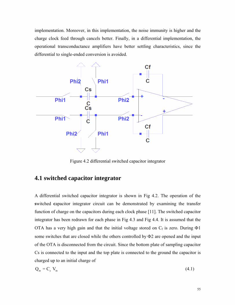
A fully differential implementation is selected to implement the converter. It offers
increase of 3dB in the signal-to-noise ratio, compared with the single-ended
54
Page 57
implementation. Moreover, in this implementation, the noise immunity is higher and the
charge clock feed through cancels better. Finally, in a differential implementation, the
operational transconductance amplifiers have better settling characteristics, since the
differential to single-ended conversion is avoided.
Figure 4.2 differential switched capacitor integrator
4.1 switched capacitor integrator
A differential switched capacitor integrator is shown in Fig 4.2. The operation of the
switched capacitor integrator circuit can be demonstrated by examining the transfer
function of charge on the capacitors during each clock phase [11]. The switched capacitor
integrator has been redrawn for each phase in Fig 4.3 and Fig 4.4. It is assumed that the
OTA has a very high gain and that the initial voltage stored on Cf is zero. During Φ1
some switches that are closed while the others controlled by Φ2 are opened and the input
of the OTA is disconnected from the circuit. Since the bottom plate of sampling capacitor
Cs is connected to the input and the top plate is connected to the ground the capacitor is
charged up to an initial charge of
in s inQ = C V (4.1)
55
Page 58
It should be noted that the output from the integrator is zero due to the fact that the initial
voltage across Cf is zero
Figure 4.3 discrete time integrator during Φ1
Figure 4.4 discrete time integrator during Φ2
During phase Φ2 all of the switches that were previously closed are all opened. Thus the
input is disconnected from the circuit and the output is no longer available from the
integrator. The bottom plate of Cs is connected to ground and top plate of Cs is connected
to the input terminal of the OTA. The connection of the OTA output to its input forces
the differential input voltage of the OTA to zero. Meanwhile since the bottom plate of Cs
is connected to ground and top plate of Cs is forced to zero due to the OTA, the charge on
the sampling capacitor Cs can only be transferred to the feedback capacitor Cf. The
56
Page 59
charge transferred is equal to
final f outQ = C V (4.2)
However this charge must be equal to the original charge sampled onto Cs. Equating Qfinal
with Qin and rearranging for the output voltage yields
sout in
f
CVC
= V (4.3)
When phase Φ1 is active again, the input voltage is sampled again onto Cs while the
integrator output voltage is equal to the previous sample multiplied by a gain factor of
Cs/Cf. Then again during Φ2 the charge from the new sampled input is transferred to the
feedback capacitor where it adds to the previous charge stored from the first sampling
operation. The charge stored on the feedback capacitor is always maintained by the OTA
and is never discharged. Thus the feedback capacitor accumulates the charge taken from
each sampling operation of the input signal. Since the output of the switched capacitor
integrator at a particular moment in time is equal to the previous output voltage in
addition to the input voltage sampled in the previous operation multiplied by a gain factor
Cs/Cf, the output of the integrator may be written mathematically as,
( ) ( [ 1]) ( [ 1]sout s out s in s
f
CV nT V T n V T nC
= − + − ) (4.4)
Taking the Z transform of equation 4.3 yields
1( ) ( ) ( )sout out in
f
CV z z V z z V zC
− −= + 1 (4.5)
And rearranging this equation for Vout (z) gives 1
1( ) ( )1
sout in
f
C zV z V zC z
−
−=−
(4.6)
Now the integrator is made to employ the bottom plate sampling technique to minimize
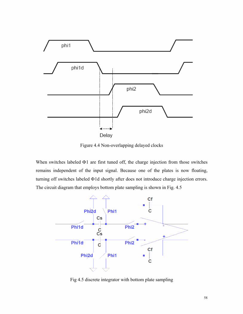
signal dependent charge injection. This is achieved through delayed clocks Φ1d and Φ2d,
which is shown in Fig. 4.4
57
Page 60
Figure 4.4 Non-overlapping delayed clocks
When switches labeled Φ1 are first tuned off, the charge injection from those switches
remains independent of the input signal. Because one of the plates is now floating,
turning off switches labeled Φ1d shortly after does not introduce charge injection errors.
The circuit diagram that employs bottom plate sampling is shown in Fig. 4.5
Fig 4.5 discrete integrator with bottom plate sampling
58
Page 61
4.2 Capacitors
It is certainly that capacitors are very important components in the design of switched
capacitor integrator. It is the best choice to implement with small capacitors when
considering area and power consumption but on the other hand when noise being
considered, large capacitors should be used.
It is well known that the noise of later stage integrators will be attenuated and shaped in
the case of practical implementation of 3rd order single loop sigma-delta modulator. Thus
the first integrator capacitors should satisfy the noise requirement, and based on this
condition smaller capacitors are preferred.
According to equation 3.12 and considering full differential input and feedback
capacitors, there are four input noise samplings, so that the total thermal noise power is
described by
4noise
KTPC
= (4.7)
Due to oversampling, the overall thermal noise power holds but the noise frequency band
spreads to
s Bf OSR f= × (4.8)
59
Page 62
Thus the thermal noise power in the base band scales to 1/OSR, which is described by
4noise
KTPC OSR
=×
(4.9)
On the other hand, when considering SNR should be larger than 98dB and leaving the
design margin, the final noise power root lower than -105dB is determined by
6105 5.6 10Pnoise dB −≤ − ≈ × (4.10)
And the capacitor value is calculated by equation 4.9 and 4.10, so that capacitor should
be larger than 4Pf. In this design, the smallest value 4Pf is taken into account.
4.3 Operational amplifier
The operational transconductance amplifier is the most important component in the
design of sigma-delta modulator. In the following, the requirement of amplifier will be
analyzed at the first step, then the comparison among different topology amplifiers will
be described, after that the best choice topology will be implemented and the bias circuit
and common mode feed back circuit also will be carried out.
Gain
As the model of equation 3.17 shows, finite voltage gain introduces, both gain and pole
position error in a switched capacitor integrator. These errors are especially important in
the first integrator, which create noise leakage at low frequency that is not canceled by
60
Page 63
the digital noise shaping network. However, since in this design the 3rd order Butterwords
filter, which is not very sensitive to the gap between ideal poles and practical coefficients,
is implemented to realize 3rd single loop modulator, the very optimistic values just should
be taken with reserve and the gain close to 60 dB should be used. At 60 dB or above this
value, the charge transfer errors are determined by the deviation of the capacitor ratios,
rather than the charge loss due to finite voltage gain.
Unit-gain bandwidth
The finite bandwidth of amplifier also introduces a gain and a pole error on the integrator
transfer function as described in Chapter 3. The gain-bandwidth has to be greater than 4
times the sampling frequency, to have a good performance.
4 6.144 24.6uf MHz= × = (4.11)
Considering providing some margin for other effects, the gain-bandwidth was pushed to a
higher frequency of about 30 MHz.
Slew rate
The one of the most destructive effect in the performance of the modulator is due to finite
output slew rate. SR determines the time available to the integrator for exponential
settling after slewing. If SR is low, this time decreases and large settling error occurs. In
the limit, only slewing takes place during the available settling time. Such a situation can
leave the modulator in an unstable condition. In order to obtain the proper performance,
the minimum SR should be calculated [25]
61
Page 64
7 85.96 /s REFSR f V V us> × × = (4.12)
As usual considered the margin again, 90V/us will be used in the OTA design.
The choice of operational transconductance amplifiers plays a critical role in the
modulator design [19]. Operational transconductance amplifiers characterized by the
absence of an output buffer and having so a high output resistance, are the ones preferred
for switched capacitor implementations. In principle, in a switched capacitor network the
operational amplifiers are embedded in an environment, in which they do not experiment
resistive loads, only a purely capacitive load, thus, the output resistance presented by the
amplifier is not a design constraint. There are mainly three OTA architectures found in
the literature [15][19][20], namely, the telescopic cascode, folded cascode, and the
two-stage OTA. There are also refinements to improve certain characteristics such as
output signal swing or voltage gain or speed of single stage architectures. Here, our
objective is to present a brief review and comparison of the main characteristics of each
fundamental topology in order to introduce the elected OTA.
Telescopic cascode OTA
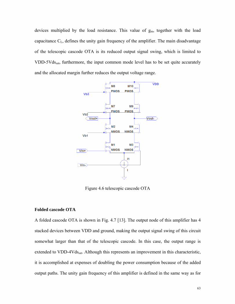
The basic implementation of a fully differential telescopic cascode OTA is shown in Fig.
4.6. The simple construction of this OTA reflects the benefits of a single stage amplifier,
namely low power consumption and high frequency response. It posses the highest
non-dominant second pole defined by the transconductance of the cascode transistors M2
and M4 as well as the parasitic capacitances at the drains of the input differential pair M1
and M3. The voltage gain of this OTA is equal to the transconductance of the input
62
Page 65
devices multiplied by the load resistance. This value of gm, together with the load
capacitance CL, defines the unity gain frequency of the amplifier. The main disadvantage
of the telescopic cascode OTA is its reduced output signal swing, which is limited to
VDD-5Vdssat, furthermore, the input common mode level has to be set quite accurately
and the allocated margin further reduces the output voltage range.
Figure 4.6 telescopic cascode OTA
Folded cascode OTA
A folded cascode OTA is shown in Fig. 4.7 [13]. The output node of this amplifier has 4
stacked devices between VDD and ground, making the output signal swing of this circuit
somewhat larger than that of the telescopic cascode. In this case, the output range is
extended to VDD-4Vdssat. Although this represents an improvement in this characteristic,
it is accomplished at expenses of doubling the power consumption because of the added
output paths. The unity gain frequency of this amplifier is defined in the same way as for
63
Page 66
the telescopic cascode, however, the second pole of this circuit is located at lower
frequencies because it is defined by the transconductance of NMOS devices M1 and
M3and the capacitance seen from the drain of these devices to ground while it is much
lager compared with telescopic architecture. This in turn lowers the phase margin. The
most attractive characteristic of this OTA is the possibility of electing the input and
output common mode range separately.
Figure 4.7 folded cascode OTA
Two-stage OTA
Fig 4.8 shows a fully differential implementation of a two-stage OTA. In contrast to the
previous topologies, this OTA achieves its voltage gain using a differential pair followed
with a common source amplifier. Stable operation of this circuit in negative feedback
loops requires the usage of internal compensation achieved by the capacitors Cc. This
compensation usually leads to a sacrifice in the gain-bandwidth as compared with single
64
Page 67
stage amplifiers. The fully differential implementation of this OTA requires two common
mode feedback circuits in order to control each stage. The main advantage of this
classical topology is the improved output signal swing with respect to that of the second
stage amplifiers, which makes this circuit a good candidate for designs with low power
supply, where the use of cascoded devices is unfeasible.
Figure 4.8 two-stage OTA
In conclusion, when compared with other topologies like two-stage amplifier, the
two-stage amplifier has a lower dominant pole than the folded cascade amplifier, hence it
cannot be used in high frequency applications. Folded cascode circuit does not need
frequency compensation as needed for a two-stage amplifier. The two-stage amplifier has
poorer power supply rejection ratio than the folded cascode circuit at high frequencies.
On the other hand, the telescopic amplifier has low output signal swing which is not
fulfill the requirement of high output swing. Hence, keeping all these aspects in mind,
Folded cascode OTA has been used extensively in switched capacitor circuits [9]. It has
65
Page 68
the advantages of high DC gain, large output swing, large bandwidth and simple structure.
Therefore it has been used successfully in many high-speed high-resolution sigma-delta
modulators. The schematic of Folded cascode OTA in our design is shown in Fig 4.9.
Fig 4.9 practical amplifier in the design
Bias circuit
In order to have the transistors stay in active region, gate voltages were supplied from a
separate block of circuitry is provided. It provides proper bias current for both PMOS and
NMOS transistors. A standard wide swing cascode current mirror [12], which is shown in
Fig. 4.10, is used to provide for the biasing of the transistors in the cascode pair. This is
one circuit that does not limit the signal swing as much as the other conventional current
mirrors and also provides higher output resistance and a better matching for the currents.
66
Page 69
Figure 4.10 wide swing biasing circuit
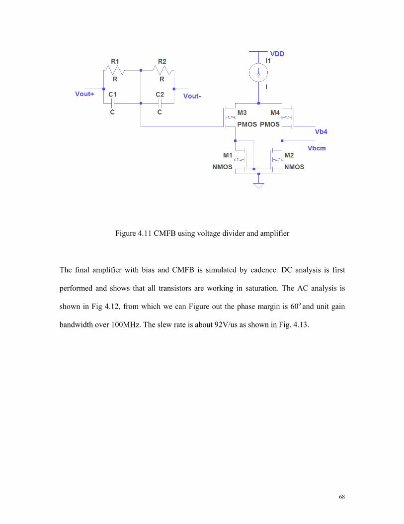
CMFB
One drawback of using full differential amplifier is that a common mode feedback
(CMFB) circuit must be used [10]. If the voltage of either one of input transistor goes
down, without the CMFB the output voltage would go even lower because of the
imbalanced voltages on the other side of transistor. In this case, the job of CMFB is to
limit the drop of the voltage on either side of transistor when the input voltages are
changing. CMFB would adjust the gate voltage of the transistors M1, M3 in the OTA so
it would balance voltage levels for both transistor ladders. The CMFB stabilizes the
common-mode voltage, which is about half way between the power-supply voltages. The
CMFB also limits the maximum voltage swing on the output signals. The CMFB in our
design is shown in Fig. 4.11, which is realized by voltage divider and amplifier [13].
67
Page 70
Figure 4.11 CMFB using voltage divider and amplifier
The final amplifier with bias and CMFB is simulated by cadence. DC analysis is first
performed and shows that all transistors are working in saturation. The AC analysis is
shown in Fig 4.12, from which we can Figure out the phase margin is 60o and unit gain
bandwidth over 100MHz. The slew rate is about 92V/us as shown in Fig. 4.13.
68
Page 71
Figure 4.12: AC Analysis of proposed amplifier
Figure 4.13 slew rate test result of proposed amplifier
69
Page 72
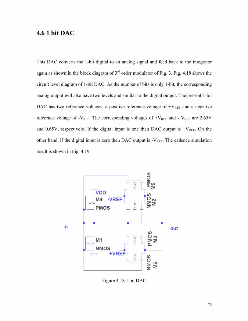
4.4 Comparator
An important component of any ADC is comparator. The comparator is widely used in
the process of converting analog signal to digital signal that is a circuit comparing an
analog signal with another analog signal or reference and outputs a binary signal based on
the comparison.
The accuracy requirement of the comparator depends on the accuracy requirement of the
converter, and conventionally a 16-bit ADC requires a comparator with at least 16-bit
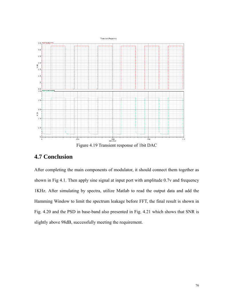
accuracy. In contrast, in sigma-delta modulator the comparator is required to work at a
high oversampling frequency but its resolution can be as small as 1 bit. Therefore, the
comparator design in sigma-delta modulator focuses more on high-speed operation
instead of accuracy.
If the output of the previous stage integrator is greater than the reference voltage then
comparator has to give an output of one and if the integrator output is less than the
reference voltage then the output of the comparator should be zero. Thus 1-bit ADC
output will have two levels, a one or zero. As VDD in our design is 3.3v, so one equals to
VDD. Similarly zero implies ground. For a given reference level, the comparator gives an
output of VDD when the signal is greater than the reference level and an output of zero
when signal is less than the reference level. Remember that the reference level VCM =
1.65v is used in our design.
70
Page 73
To combine the sample and hold function and the comparator function and also to match
speeds, a latched comparator is the best choice [14], which is used here to synchronize
its operation with the other circuits in the ADC as they are run by high speed clocks. The
topology of the comparator is shown in Fig. 4.14,
Figure 4.14 high speed latched comparator
The operation of the comparator is described as following,M1 and M6 are the
discharge-current-controlling transistors which are connected to a feedback network
formed by M5 and M2; M3 and M7 are transfer gates for strobing; M13 and M9 form
another regenerative feedback; M10 and M14 are precharge transistors; M8, M12, M11
and M4 formed two inverters which act as buffers to isolate the latch from the output load
71
Page 74
and to amplify the comparator output.
During the pre-charge phase, i.e. when Vclk goes low, transistors M3 and M7 are cut off
and the comparator does not respond to any input signal. The voltages V1+ and V1- will be
pulled to positive rail, VDD, and the output of the inverters will be pulled to ground. At
the same time, M1 and M6 discharge the voltages V2+ and V2- to ground.
During the evaluation phase, i.e. when Vclk goes high, both the voltages V2+ and V2- drop
from the positive rail and both the voltages V1+ and V1- rise from ground initially. If the
voltage at Vin+ is higher than that at Vin-, M1 draws more current than M6. Thus, V2+
drops faster than V2- and V1- rises faster than V1+. As V2+ drops a threshold voltage below
VDD, M9 turns on and charge V2- to high level while V2+ keeps going to ground. Also, as
V1- rises a threshold voltage above ground, M5 turns on and discharge V1+ to ground
while V1- keeps rising to VDD.
The regenerative action of M13 and M9 together with that of M5 and M2 pulls V2+ to
ground and pulls V2- to positive rail. Hence, following the inverters Vout+ is pulled to
positive rail and Vout- is pulled to ground. The operation for the case when the voltage at
Vin- is higher than that at Vin+ is similar.
the cadence corresponding simulation result is shown in Fig 4.15 with reference voltage
1.65V.
72
Page 75
Figure 4.15 simulation result of proposed comparator
4.5 Clock phase generation
Switched capacitor circuits require the generation of two-phase non-overlapping clocks
with delayed clocks to reduce the signal-dependent charge injection. The clock generator
for producing non-overlapping clock signals can be realized with a simple circuit
constructed with logic gates. Such a circuit is shown in Fig. 4.16. It consists of two NOR
gates and several inverters. The main advantage of this circuit is its simplicity. At least a
part of the buffering of output signals can be included in the delay elements, making the
circuit quite robust. The expecting time wave is shown in Fig 4.17.
73
Page 76
Figure 4.16 non-overlapping clock generation
Figure 4.17 Clock waveforms
74
Page 77
4.6 1 bit DAC
This DAC converts the 1-bit digital to an analog signal and feed back to the integrator
again as shown in the block diagram of 3rd order modulator of Fig. 3. Fig. 4.18 shows the
circuit level diagram of 1-bit DAC. As the number of bits is only 1-bit, the corresponding
analog output will also have two levels and similar to the digital output. The present 1-bit
DAC has two reference voltages, a positive reference voltage of +VREF and a negative
reference voltage of -VREF. The corresponding voltages of +VREF and - VREF are 2.65V
and 0.65V, respectively. If the digital input is one then DAC output is +VREF. On the
other hand, if the digital input is zero then DAC output is -VREF. The cadence simulation
result is shown in Fig. 4.19.
Figure 4.18 1 bit DAC
75
Page 78
Figure 4.19 Transient response of 1bit DAC
4.7 Conclusion After completing the main components of modulator, it should connect them together as
shown in Fig 4.1. Then apply sine signal at input port with amplitude 0.7v and frequency
1KHz. After simulating by spectra, utilize Matlab to read the output data and add the
Hamming Window to limit the spectrum leakage before FFT, the final result is shown in
Fig. 4.20 and the PSD in base-band also presented in Fig. 4.21 which shows that SNR is
slightly above 98dB, successfully meeting the requirement.
76
Page 79
0 500 1000 1500 2000 2500 3000 3500-160
-140
-120
-100
-80
-60
-40
-20
0
Frequency KHz
dB
Figure 4.20 FFT result of the proposed modulator
-60 -40 -20 0 20 40 60 80
-150
-100
-50
0
Frequency KHz
dB
98.9dB
Figure 4.21 PSD in the base-band
77
Page 80
Chapter 5
Conclusion
This thesis was mainly concerned with analysis, modeling and design of sigma-delta
modulators for audio application by top-down approach. The final design was a 16-bit,
3rd order single loop one bit sigma-delta modulator with an oversampling ratio of 128.
The design was divided into two parts from system level to circuit level. At the system
level, the modulator architecture was discussed and determined as well as non-idealities
analysis. Then the circuits were designed in TSMC 0.35um technology at an operating
voltage of 3.3 V. A fully differential switched capacitor implementation was used. Main
important components such as operational amplifier, comparator, non-overlapping clock
generator and feedback DAC are also studied and designed.
There are some possible future works that can be done to optimize this project. One of
the works is using different topology loop to implement the modulator and compare with
the current project. In addition, more non-idealities could be taken into account, such as
non-linearity of amplifier DC gain.
Another important works could improve the project is decimation filter. This decimation
filter performs two important functions. First, it low-pass filters the output signal from
the quantizer so that all frequency components above fB are removed. Hence, this
78
Page 81
filtering action removes all of the quantization noise that does not appear within the
bandwidth. The second function that it performs is to downsampling the data from the
oversampling frequency of fs to the Nyquist rate of the input signal. Note that the filtering
action that precedes the down-sampling operation ensures that aliasing does not occur.
Hence due to these functions the decimation filter is one of the important blocks.
79
Page 82
Reference
[1] Alan V. Oppenheim, Alan S. Willsky, with S. Hamid, S. Hamid Nawab, “Signal and
System”, Prentice Hall Signal Processing Series.
[2] Oppenheim A V, Schafer R W, “Discrete-Time Signal Processing”, Prentice Hall
Signal Processing Series.
[3] John G. Proakis, Dimitris G. Manolakis, “Digital Signal Processing principle,
algorithms, and application” 3rd Edition.
[4] John G. Proakis, “digital communication”, McGraw-Hill Science press.
[5] Rudy Van De Plassche, “Integrated Analog-to-digital And Digital-to-analog
Converters” Kluwer Academic Publishers.
[6] Aziz, P.M., Sorensen, H.V., Vander Spiegel J. “An overview of sigma-delta
converters” Signal Processing Magazine, IEEE Volume: 13, Issue: 1, pp. 61 – 84.
Jan. 1996
[7] Ho Yoon San, Hasan S M R, “Low power, high performance switched-capacitor
sigma-delta modulator suitable for battery operated audio signal processing
applications”. 1996 IEEE TENCON - Digital Signal Processing Applications,
Volume 2, 26-29 November 1996, Page(s): 728 – 73
[8] Richard Schreier, Gabor C. Temes, “Understanding Delta-Sigma Data Converters”,
IEEE press.
[9] Bingxin Li and Hannu Tenhunen “A Design of Operational Amplifiers for Sigma
Delta Modulators using 0.35um CMOS Process”
80
Page 83
[10] Allen P E, Holberg D R, “CMOS Analog Circuit Design”, Oxford University Press.
[11] Johns D A, Martin K, “Analog Integrated Circuit Design”, John Wiley and Sons
Inc.,
[12] Takeshi Fukumoto, Hiroyuki Okada, Kazuyuki Nakamura “Optimizing Bias-circuit
Design of Cascode Operational Amplifier for Wide Dynamic Range Operations”
ISLPED ’01, August 6-7, 2001, Huntington Beach, California, USA.
[13] Razavi B, “Design of Analog CMOS Integrated Circuits”, McGraw-Hill
PublishingCompany Limited.
[14] Yukawa A, “A CMOS 8-bit high-speed A/D converter IC”, Solid-State Circuits,
IEEE Journal of, Volume SC-20, Issue 3, June 1985.
[15] Gray P R, Meyer R G, “MOS Operational Amplifier Design-Tutorial Overview”,
Solid-State Circuits, IEEE Journal of, Volume SC-17, Issue 6, December 1982,
Page(s): 969-982.
[16] SIMULINK and MATLAB Users Guides, The MathWorks, Inc., Natick, MA, 1997.
[17] P. Malcovati, S. Brigati, F. Francesconi, F. Maloberti, P. Cusinato, and A.
Baschirotto, “Behavioral Modeling of Switched-Capacitor Sigma–Delta
Modulators” ieee transactions on circuits and system, vol. 50, pp. 352- 364, march
2003
[18] Boser B E, Wooley B A, “The design of sigma-delta modulation analog-todigital
converters”. Solid-State Circuits, IEEE Journal of, Volume 23, Issue 6, December
1988 Page(s): 1298 – 1308.
[19] Rabii S, Wooley B A, “A 1.8V Digital-Audio Sigma-Delta Modulator in 0.8μm
CMOS”, Solid-State Circuits, IEEE Journal of, Volume 32, Issue 6, June 1997,
81
Page 84
Page(s): 783- 796.
[20] P. R. Gray, P. J. Hurst, S. H. Lewis, and R. G. Meyer, “Analysis and Design of
Analog Integrated Circuits”, 4th edition, John Wiley & Sons, 2001.
[21] A. R. Feldman, “High speed, low-power sigma-delta modulator for RF base-band
channel application” Ph.D. Dissertation, University of California Berkeley, 1997
[22] S. Rabii and B. A. Wooley, “The Design of Low-Voltage, Low-Power Sigma-Delta
Modulators”. Kluwer Academic Publishers, 1999.
[23] S. R. Norsworthy, R. Schreier, and G. C. Temes, “Delta-Sigma Data Converters :
Theory, Design, and Simulation”. Wiley-IEEE Press, 1996.
[24] Ulrik Sørensen Wilsmar Low-power, “Low-voltage Analog to Digital sigma-delta
modulators”, PhD thesis, 2006
[25] A 15-bit 2 MHz Nyquist rate ΔΣ ADC in a 1 µm CMOS technology Marques, A.;
Peluso, V. Steyaert, M. Sansen, W. Solid-State Circuits Conference, 1997. ESSCIRC
apos. Proceedings of the 23rd European Volume, Issue , 16-18 Sept. 1997 Page(s): 68-71
[26] Zare-Hoseini, H. Kale, I. Shoaei, “Modeling of switched-capacitor delta-sigma
Modulators in SIMULINK” Instrumentation and Measurement, IEEE Transactions
on Volume 54, Issue 4, Aug. 2005 Page(s): 1646 - 1654
[27] Fornasari, A.; Malcovati, P.; Maloberti, F “Improved modeling of sigma-delta
modulator non-idealities in Simulink” Circuits and Systems, 2005. ISCAS 2005.
IEEE International Symposium on Volume , Issue , 23-26 May 2005 Page(s): 5982 -
5985 Vol. 6
82