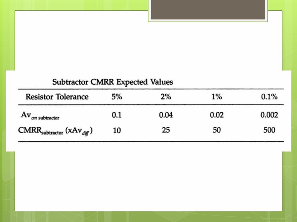
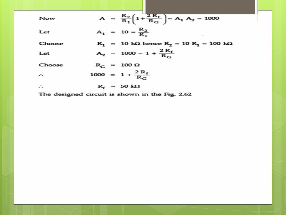
76
Design of Instrumentation Amplifier By Dr Ravi Kumar Jatoth Asst Professor ECE Department

Design of
Instrumentation
Amplifier By
Dr Ravi Kumar Jatoth
Asst Professor
ECE Department
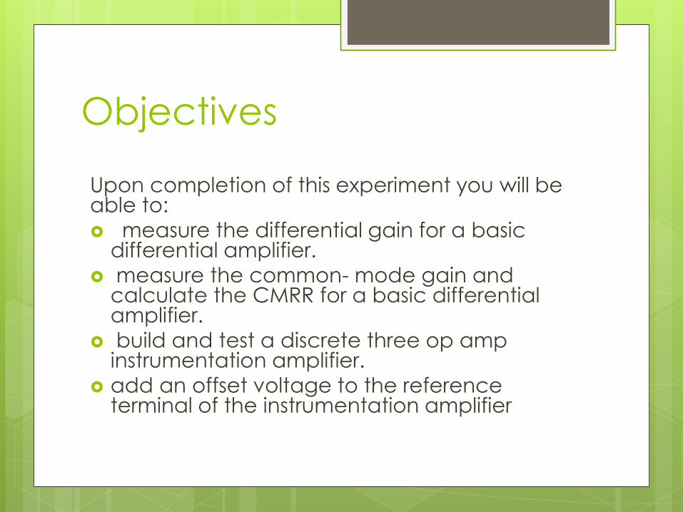
Objectives
Upon completion of this experiment you will be able to:
measure the differential gain for a basic differential amplifier.
measure the common- mode gain and calculate the CMRR for a basic differential amplifier.
build and test a discrete three op amp instrumentation amplifier.
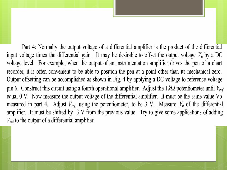
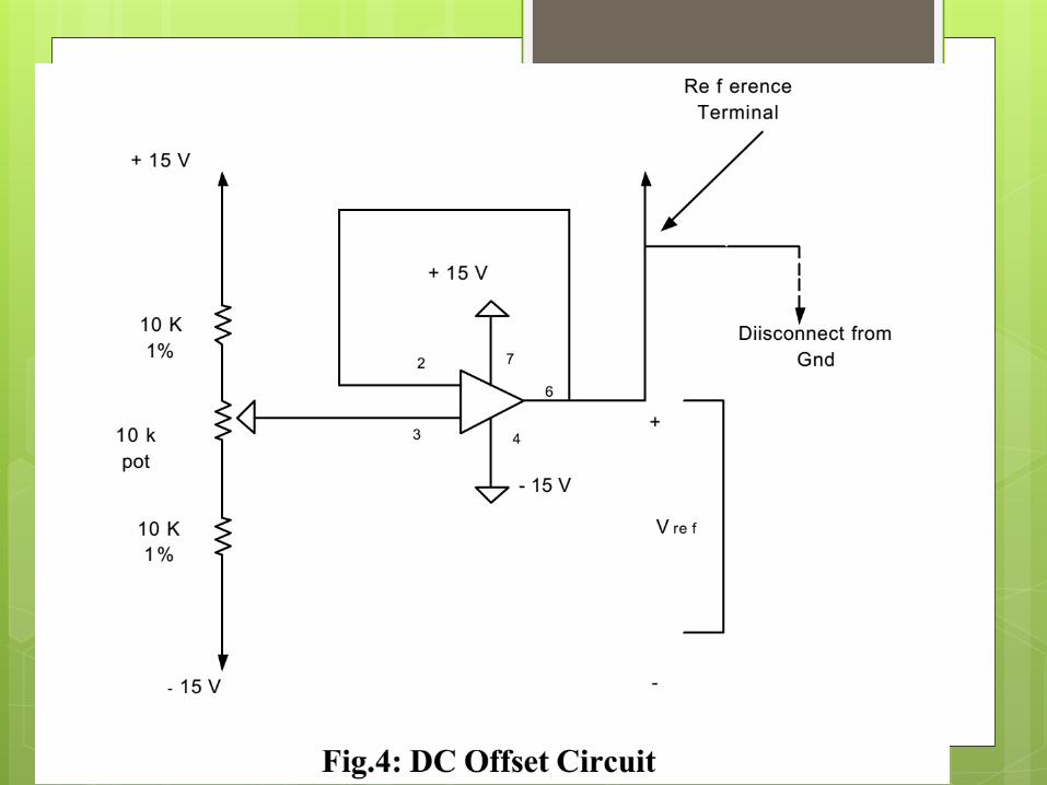
add an offset voltage to the reference terminal of the instrumentation amplifier

Ideal Characteristics of an
Amplifier
High common mode rejection
ratio(CMRR)
High input impedance
High slew rate
Low output impedance
Low power consumption
Low thermal and time drift

WHErE ArE In-AMPS AnDDIFFErEncE
AMPS USED?
Data Acquisition
Medical Instrumentation Monitor and
control Electronics
Software-Programmable Applications .
Audio Applications High Speed Signal
conditioning Video Applications
Power control Applications

Instrumentation Amplifiers
Passive Transducer Measurement Configuration:
For passive transducers in a bridge configuration the voltage of interest is the
differential voltage e = VB - VA
Therefore need a difference amplifier with a committed adjustable gain Ad
Want Vo = Ad(VB - VA) = Ad e
VCM =
Want to reject VCM
V V EA B
2 2R
R R
R+DR
IA
Vo = Ad
e

Instrumentation Amplifiers:
Active Transducer Measurement Configuration:
For an active transducer the differential voltage e
created by the transducer is of interest
Therefore need a difference amplifier
with a committed adjustable gain Ad
Want Vo = Ad e
Surface whose temperature
is to be measured may be at
some non-zero potential (VCM)
relative to ground
Want to reject VCM
IA
Vo = Ad e
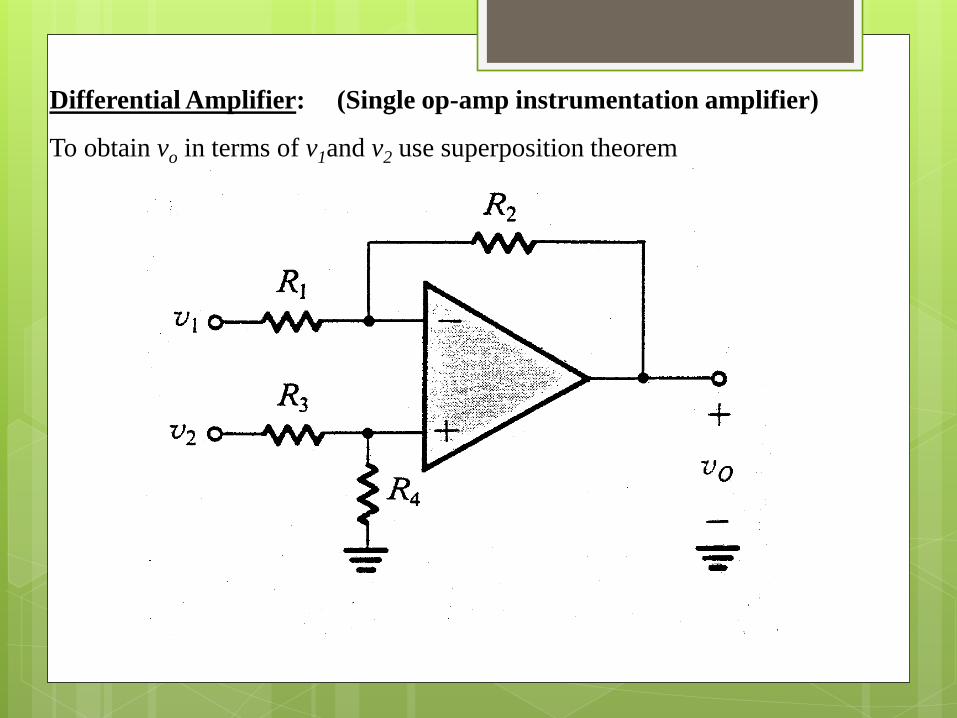
Differential Amplifier: (Single op-amp instrumentation amplifier)
To obtain vo in terms of v1and v2 use superposition theorem
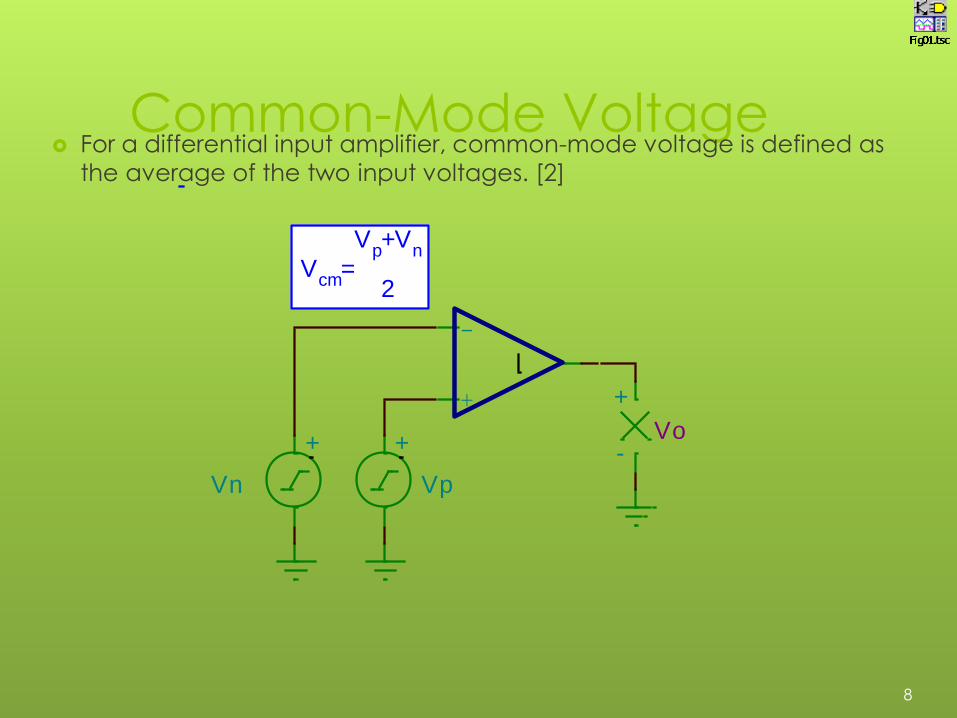
Common-Mode Voltage For a differential input amplifier, common-mode voltage is defined as
the average of the two input voltages. [2]
8
-
++
Vp
+
Vn
-
+
Vo
Vcm
=
Vp+V
n
2

Common-Mode Voltage (Alternate defn.)
• For a differential amplifier, common-mode voltage is defined as the average of the two input voltages. [2]
gain mode-Common
gain mode-alDifferenti
where
cm
dm
cmcmiddmout
A
A
VAVAV
9
-
+
Vout
Vcm
-
+
Vid
Vid/2Vid/2
-
+
IOP1
Vcm
=
Vp+V
n
2
w here
Vp=V
cm+
Vid
2
Vn=V
cm-
Vid
2

Common-Mode Voltage • Ideally a differential input amplifier only responds to a differential input voltage, not
a common-mode voltage.
10
V-
V+V-
V+
Vb 0 Va 0
-
+
Vid
Vs+ 5
Vs- 5
Vcm 0
-
++3
2
6
74 OP1
-
+
Vo 0V
0V
V-
V+
Vb 0 Va 0
-
+
Vid
Vcm 1
-
++3
2
6
74 OP1
-
+
Vo 0V
0V
V-
V+
Vb 0 Va 1m
-
+
Vid
Vcm 1
-
++3
2
6
74 OP1
-
+
Vo 3.826745V
1000uV
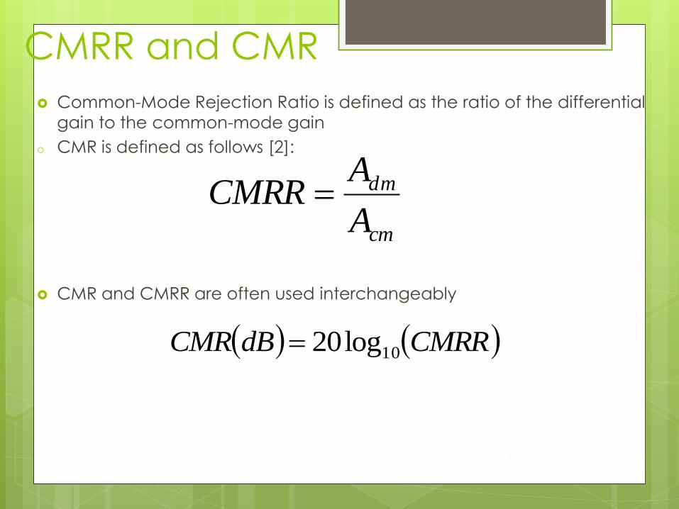
CMRR and CMR
Common-Mode Rejection Ratio is defined as the ratio of the differential
gain to the common-mode gain
o CMR is defined as follows [2]:
CMR and CMRR are often used interchangeably
cm
dm
A
ACMRR
CMRRdBCMR 10log20
11

Ideal Differential Amplifier CMRR
• What is the CMRR of an ideal differential input amplifier (e.g. op-amp)?
• Recall that the ideal common-mode gain of a differential input amplifier is 0.
• Voltage Amplifier Model [1]
• Also recall the differential gain of an ideal op-amp is infinity.
• So
cm
dm
cm
dmOAideal
A
A
A
ACMRR
12
Vs
Rs
Ri
-
+
-
+
VCVS
-
+
Vi Vi
Ro
Rload-
+
Vo
Source Amplif ier
Adm
->Infinity
Load

Real Op-Amp CMRR In an operational amplifier, the differential
gain is known as the open-loop gain.
The open-loop gain of an operational
amplifier is fixed and determined by its
design
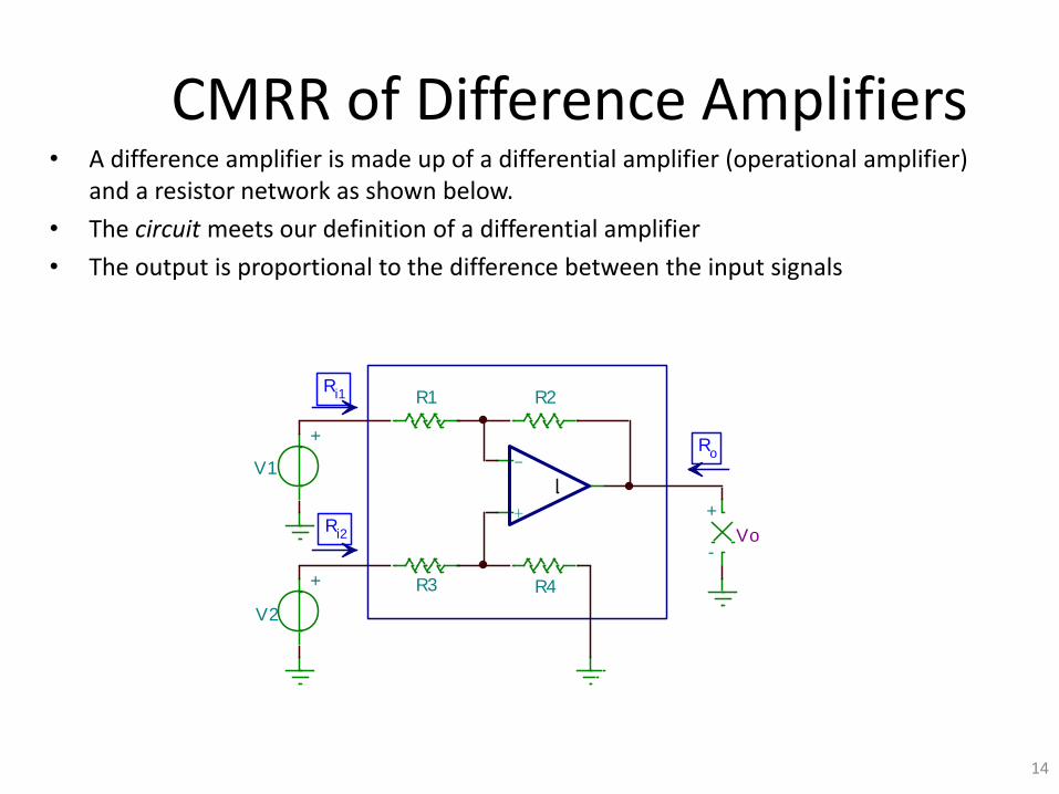
CMRR of Difference Amplifiers • A difference amplifier is made up of a differential amplifier (operational amplifier)
and a resistor network as shown below.
• The circuit meets our definition of a differential amplifier
• The output is proportional to the difference between the input signals
14
-
+
R3 R4
R1 R2
+
V1
+
V2
-
+
Vo
Ri1
Ri2
Ro
2
2
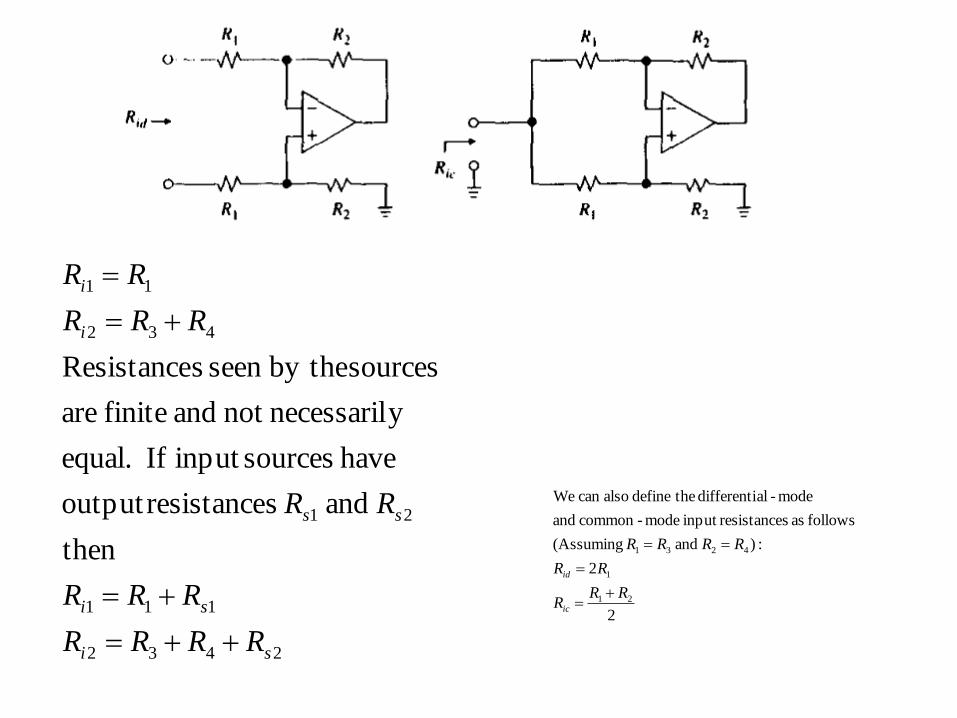
:) and (Assuming
follows as sresistanceinput mode-common and
mode-aldifferenti thedefine alsocan We
21
1
4231
RRR
RR
RRRR
ic
id
2432
111
21
432
11
then
and sresistanceoutput
have sourcesinput If equal.
ynecessarilnot and finite are
sources by theseen sResistance
si
si
ss
i
i
RRRR
RRR
RR
RRR
RR
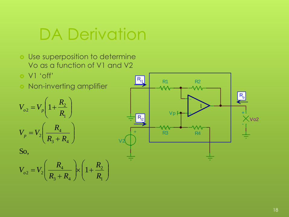
DA Derivation
Use superposition to determine
Vo as a function of V1 and V2
V1 ‘off’
Non-inverting amplifier
1
2
43
422
43
42
1
22
1
So,
1
R
R
RR
RVV
RR
RVV
R
RVV
o
p
po
18
Vp
-
+
R3 R4
R1 R2
+
V2
-
+
Vo2
Ri1
Ri2
Ro
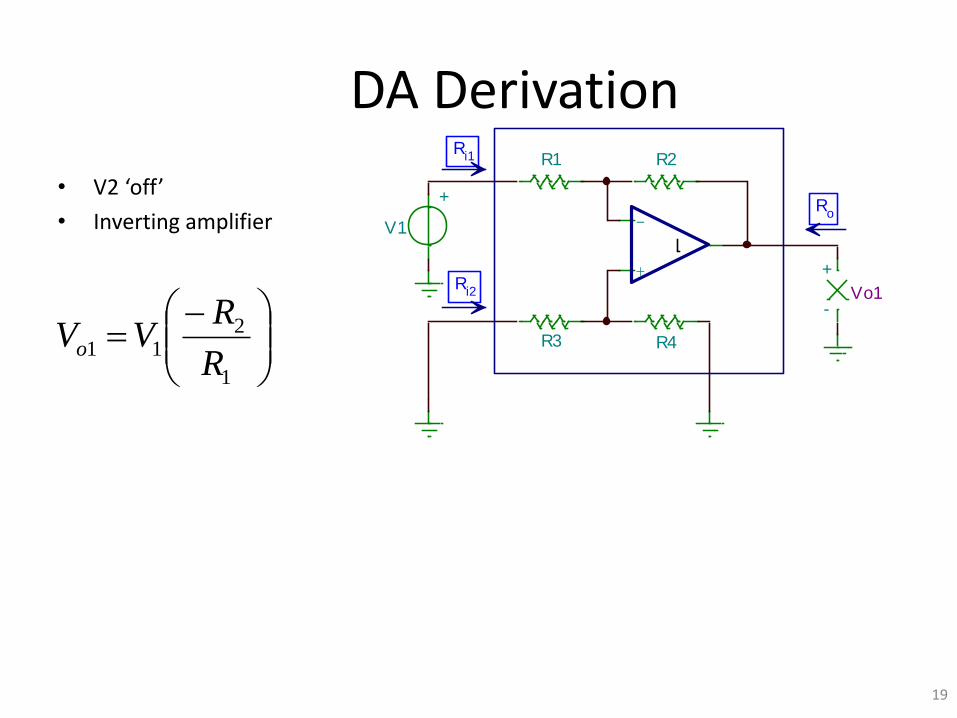
DA Derivation
• V2 ‘off’
• Inverting amplifier
1
211
R
RVVo
19
-
+
R3 R4
R1 R2
+
V1
-
+
Vo1
Ri1
Ri2
Ro
DA Derivation
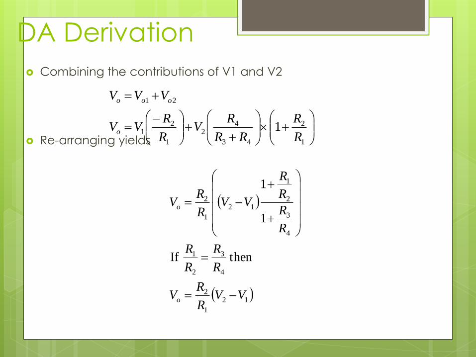
Combining the contributions of V1 and V2
Re-arranging yields
1
2
43
42
1
21
21
1R
R
RR
RV
R
RVV
VVV
o
ooo
12
1
2
4
3
2
1
4
3
2
1
12
1
2
then If
1
1
VVR
RV
R
R
R
R
R
R
R
R
VVR
RV
o
o
20

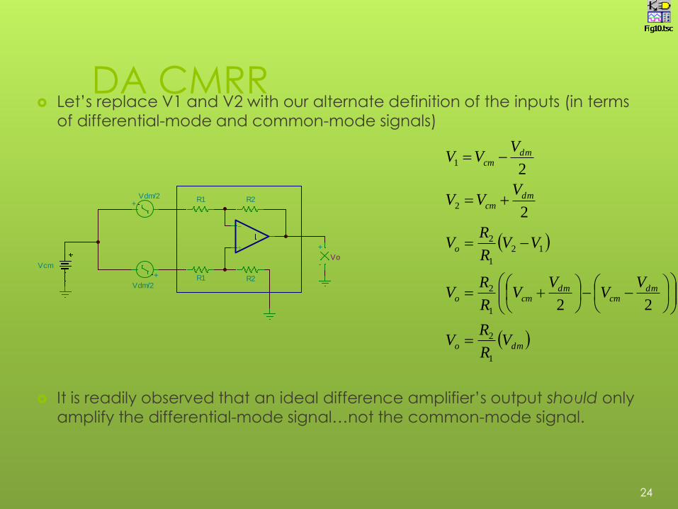
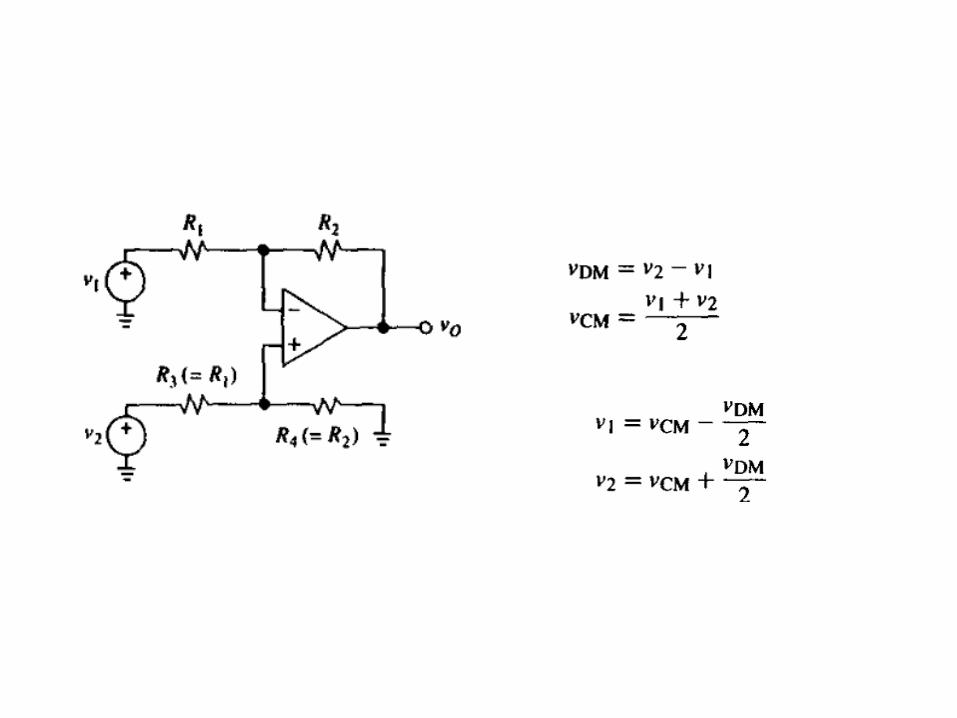
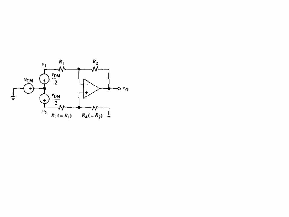
DA CMRR Let’s replace V1 and V2 with our alternate definition of the inputs (in terms
of differential-mode and common-mode signals)
It is readily observed that an ideal difference amplifier’s output should only amplify the differential-mode signal…not the common-mode signal.
24
dmo
dmcm
dmcmo
o
dmcm
dmcm
VR
RV
VV
VV
R
RV
VVR
RV
VVV
VVV
1
2
1
2
12
1
2
2
1
22
2
2
-
+
R1 R2
R1 R2
-
+
VoVcm
+
Vdm/2
+Vdm/2

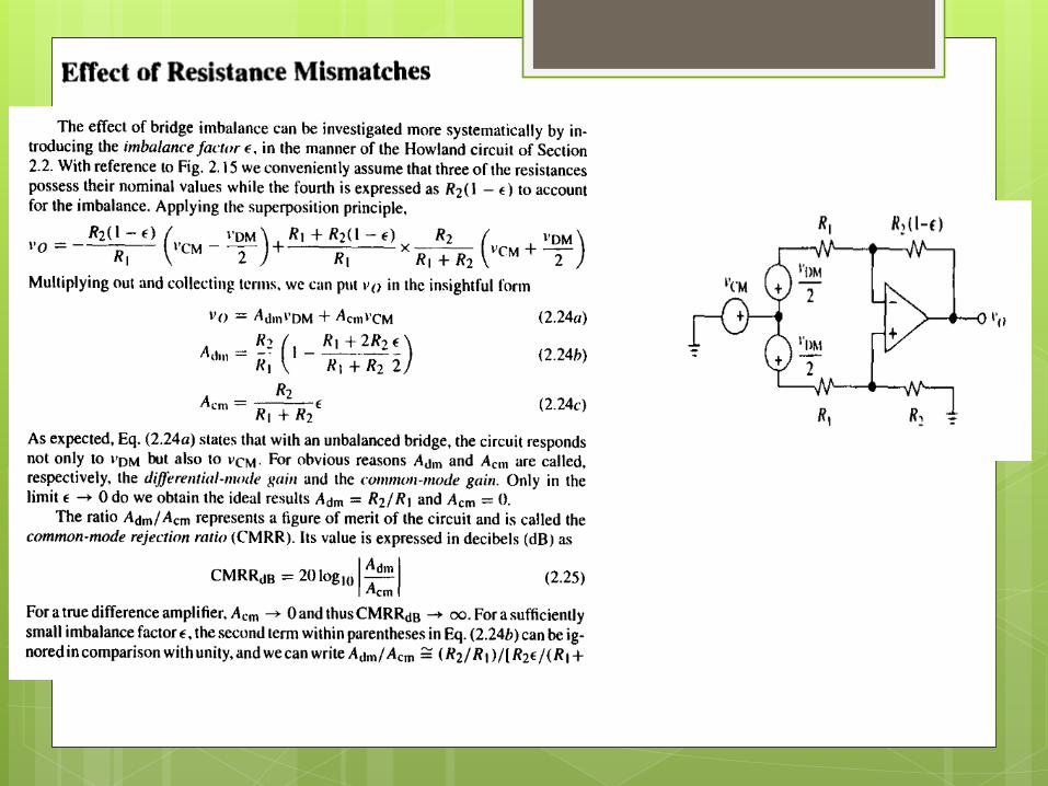
DA CMRR This assumes that the operational amplifier is ideal and that the resistors
are balanced.
Keeping the assumption that the operational amplifier is ideal, let’s see
what happens when an imbalance factor (ε) is introduced.
25
-
+
R1 R2
R1
-
+
VoVcm
+
Vdm/2
+Vdm/2 R2(1- )

DA CMRR Using superposition we find that
After some algebra we find that [1]
As expected, an imbalance affects the differential and common-mode gains, which will affect CMRR!
As the error->0, Adm->R2/R1 and Acm->0.
1
11
2
1
2 21
2
21
2
1
2
RR
R
RR
RVV
R
RVVV dm
cmdm
cmo
21
2
21
21
1
2
2
21
where
RR
RA
RR
RR
R
RA
VAVAV
cm
dm
cmcmdmdmo
26
DA CMRR
Since we have equations for Acm and Adm, let’s look at CMR
If the imbalance is sufficiently small we can neglect its effect on Adm
With that and some algebra we find [1]
1
2
10
1
log20)(R
R
dBCMR
21
2
21
21
1
2
1010
2
21
log20log20)(
RR
R
RR
RR
R
R
A
AdBCMR
cm
dm
27
DA CMRR
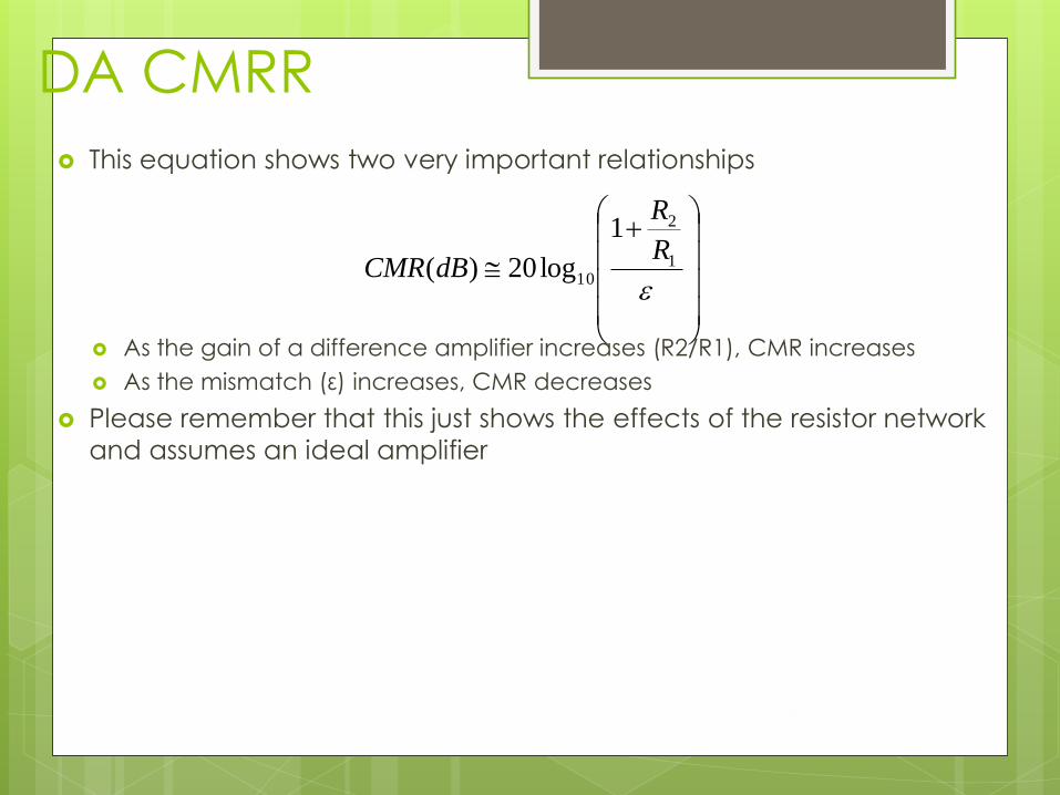
This equation shows two very important relationships
As the gain of a difference amplifier increases (R2/R1), CMR increases
As the mismatch (ε) increases, CMR decreases
Please remember that this just shows the effects of the resistor network
and assumes an ideal amplifier
1
2
10
1
log20)(R
R
dBCMR
28

DA CMRR Another possible source for CMRR degradation is the impedance at
the reference pin.
So far we have connected this pin to low-impedance ground.
Placing and impedance here will disturb the voltage divider we come
across during superposition analysis.
This will negatively affect CMR
29
-
+
R1 R2
R1 R2
-
+
VoVcm
+
Vdm/2
+Vdm/2

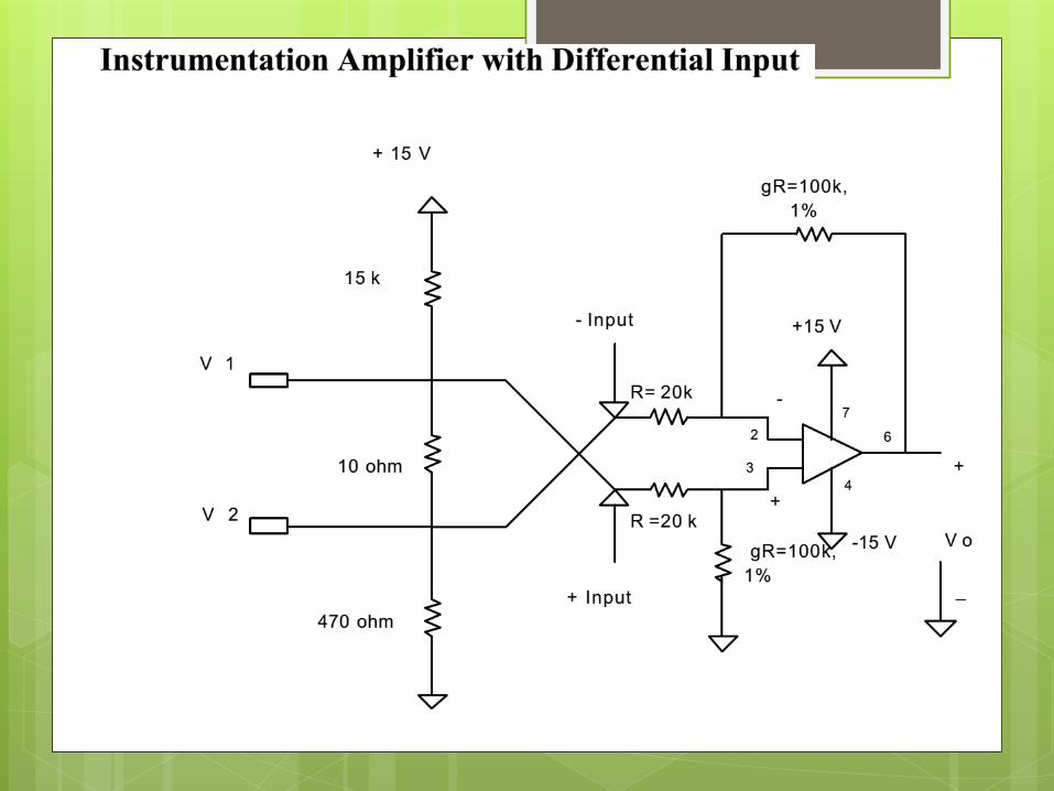
Instrumentation Amplifiers:
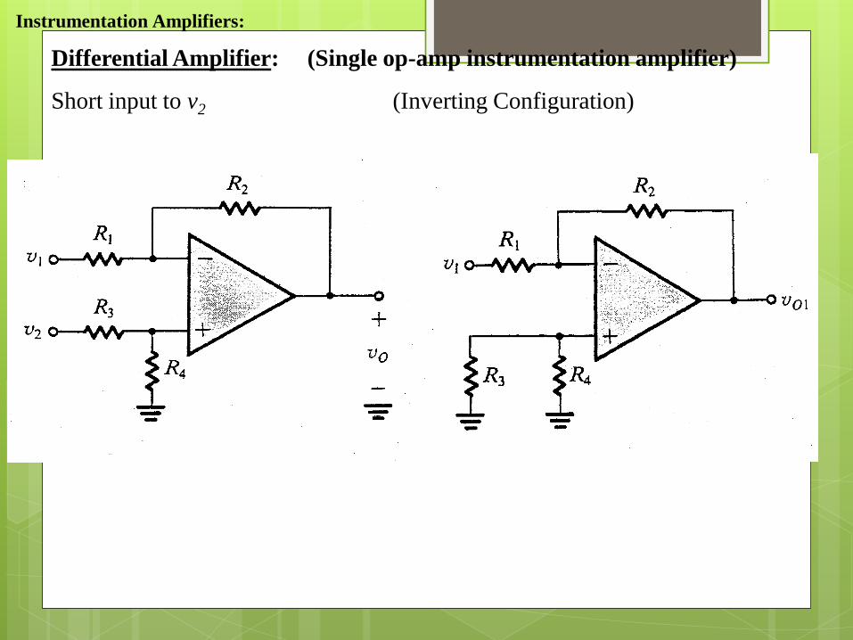
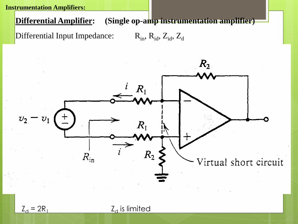
Differential Amplifier: (Single op-amp instrumentation amplifier)
Short input to v2 (Inverting Configuration)
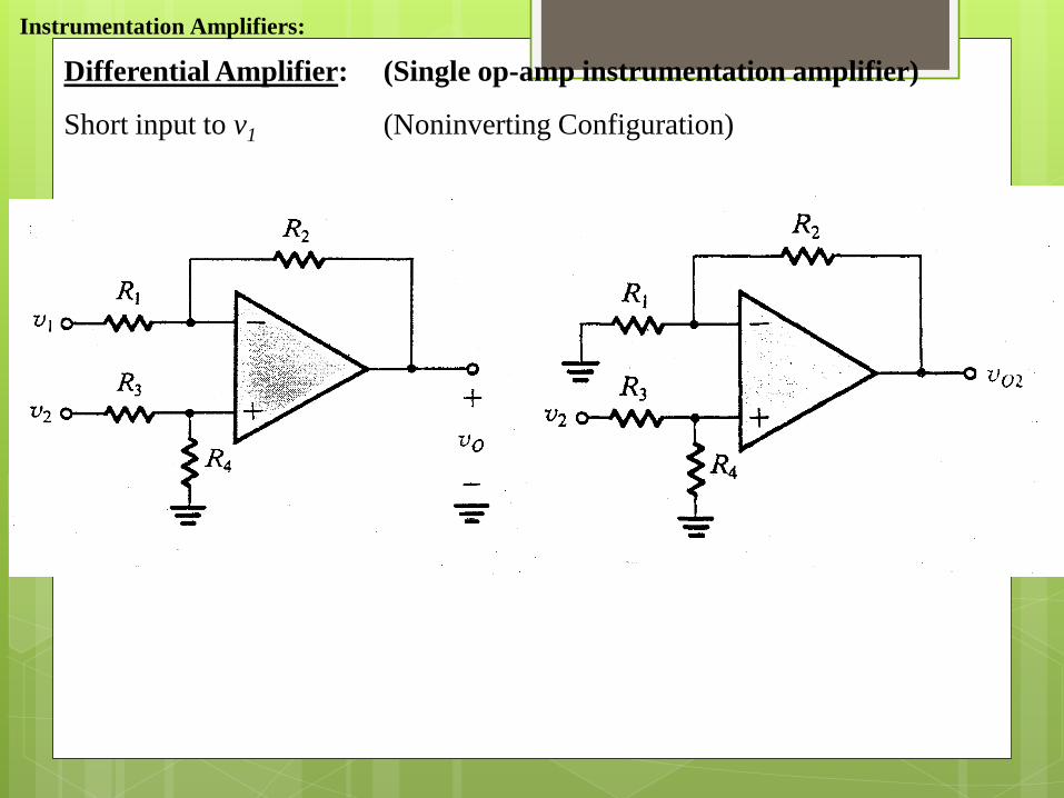
Instrumentation Amplifiers:
Differential Amplifier: (Single op-amp instrumentation amplifier)
Short input to v1 (Noninverting Configuration)
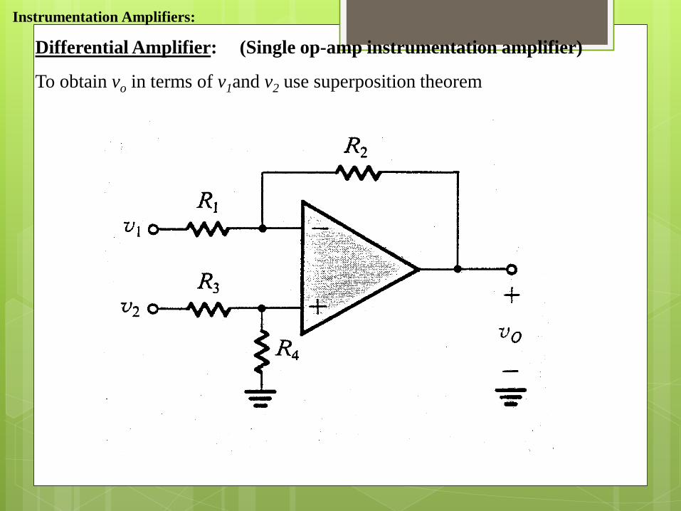
Instrumentation Amplifiers:
Differential Amplifier: (Single op-amp instrumentation amplifier)
To obtain vo in terms of v1and v2 use superposition theorem
Instrumentation Amplifiers:
Differential Amplifier: (Single op-amp instrumentation amplifier)
Differential Input Impedance: Rin, Rid, Zid, Zd
Zd = 2R1 Zd is limited
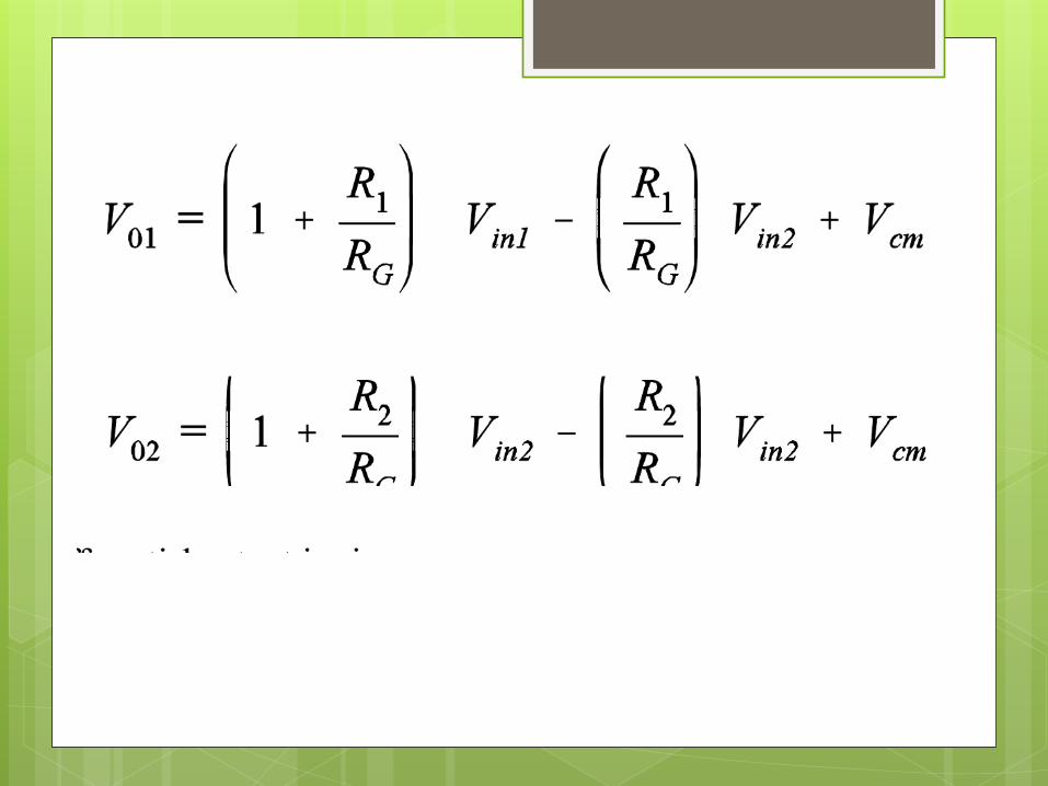
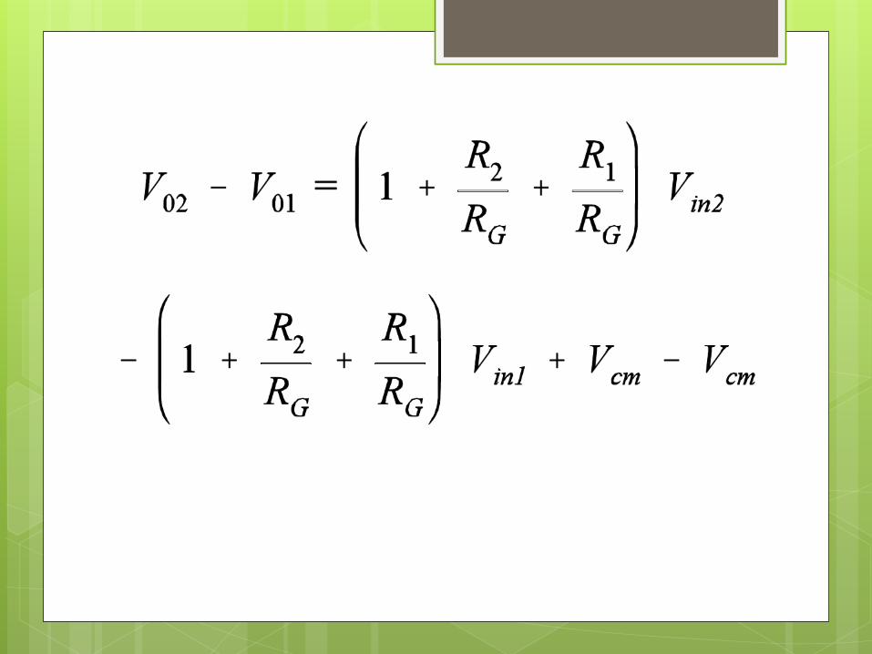
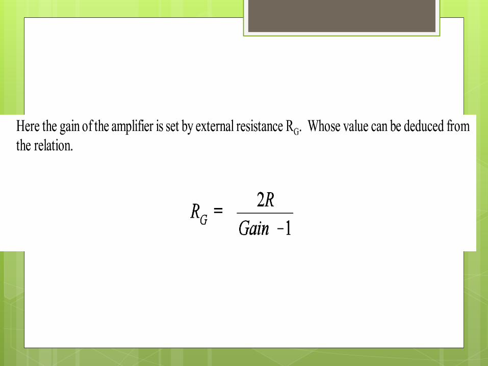
Instrumentation Amplifiers:
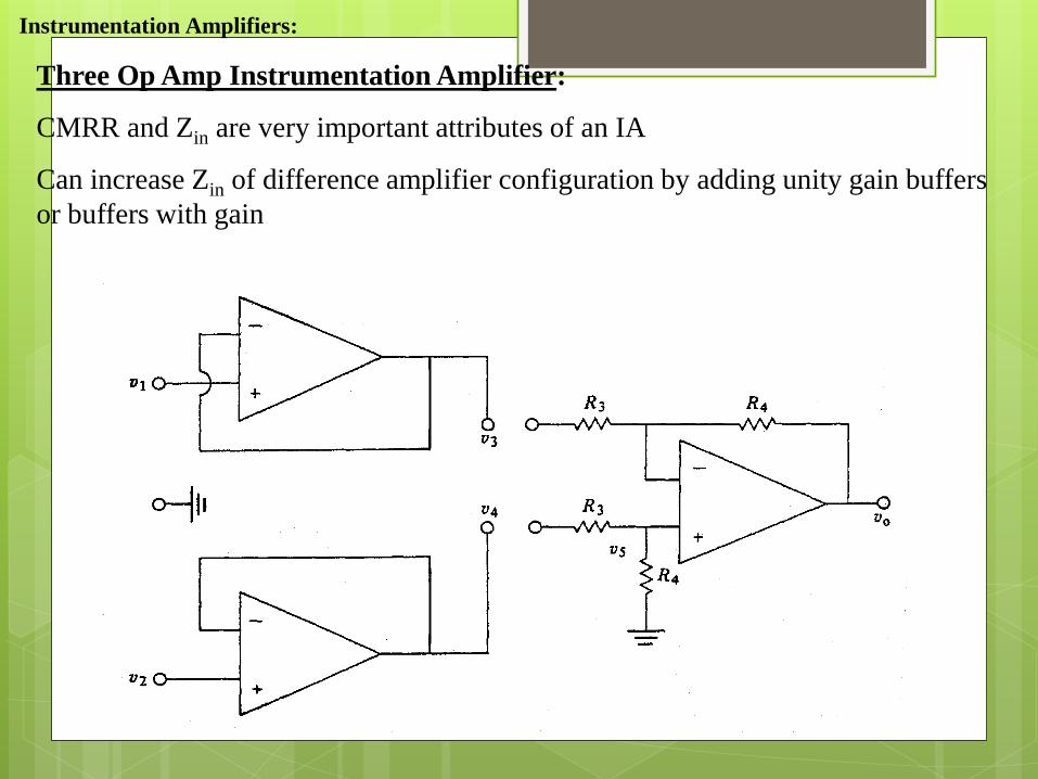
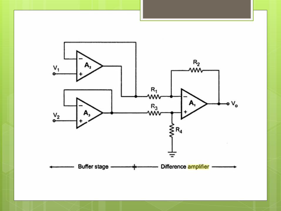
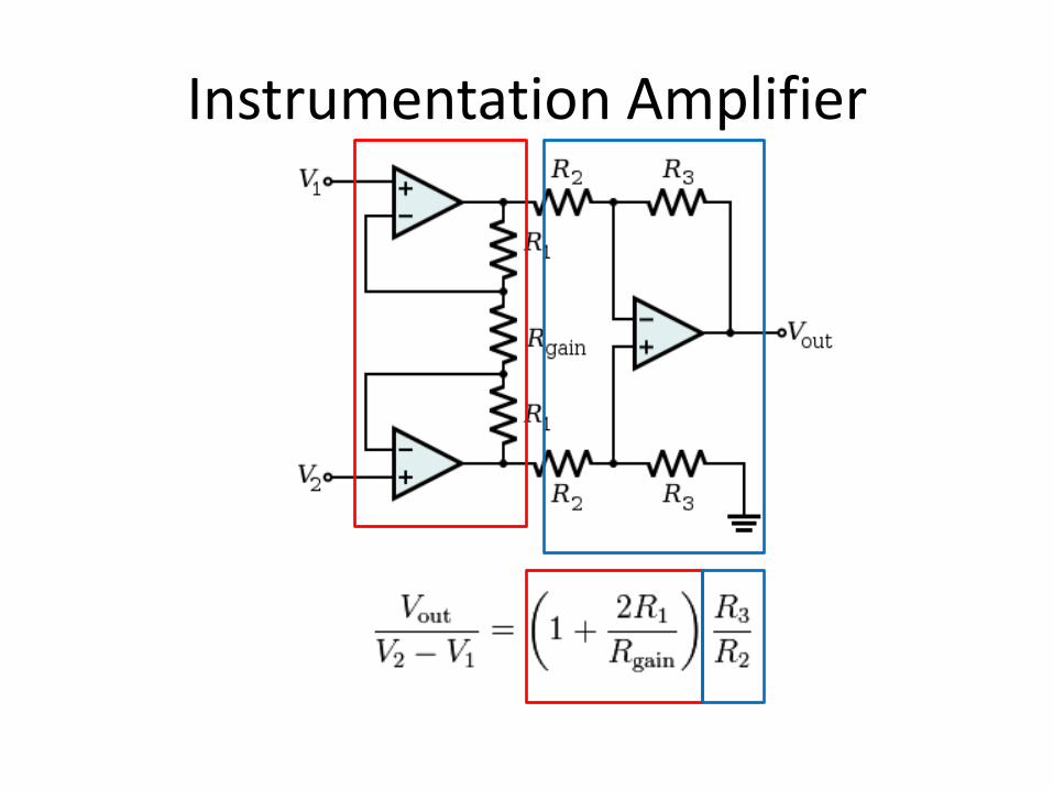
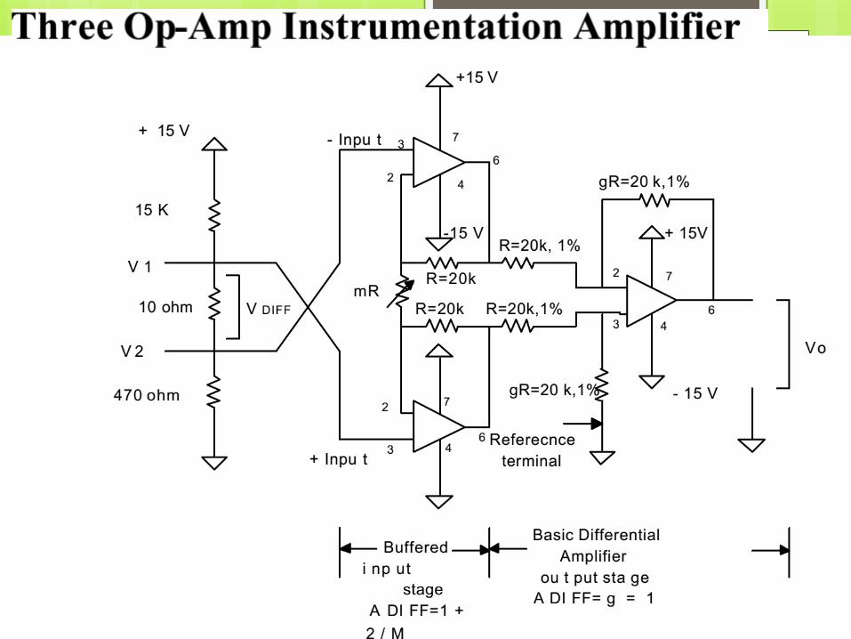
Three Op Amp Instrumentation Amplifier:
CMRR and Zin are very important attributes of an IA
Can increase Zin of difference amplifier configuration by adding unity gain buffers
or buffers with gain

Instrumentation Amplifiers:
Three Op Amp Instrumentation Amplifier:
CMRR and Zin are very important attributes of an IA
Can increase Zin of difference amplifier configuration by adding buffers
Common mode signals are not amplified if common R1 is used and
connection to ground is removed.
Instrumentation Amplifiers:
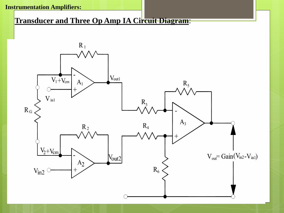
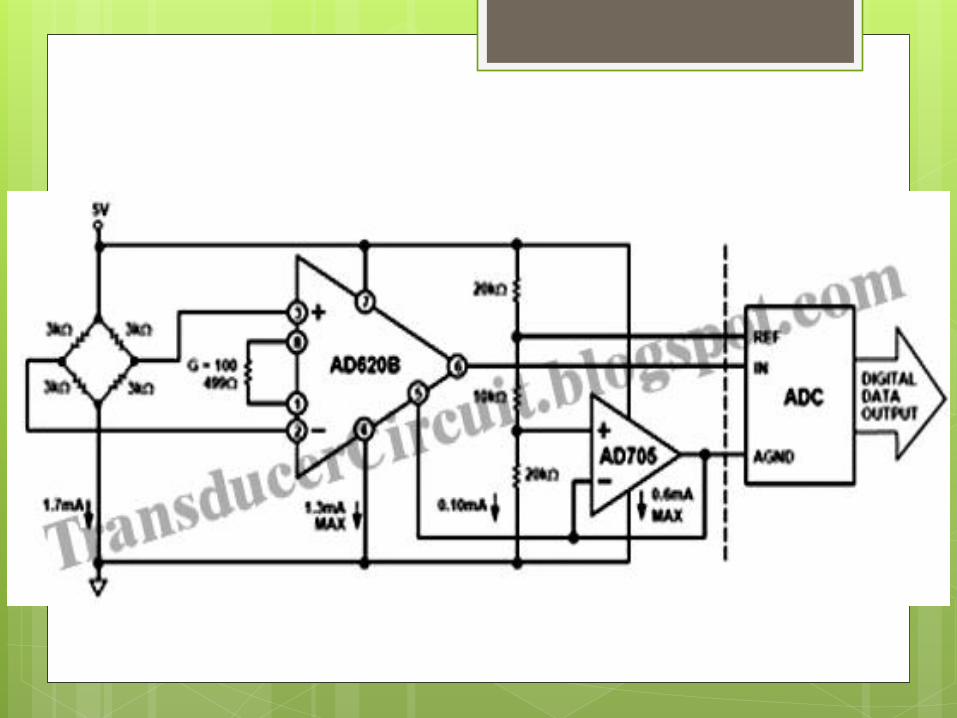
Transducer and Three Op Amp IA Circuit Diagram:


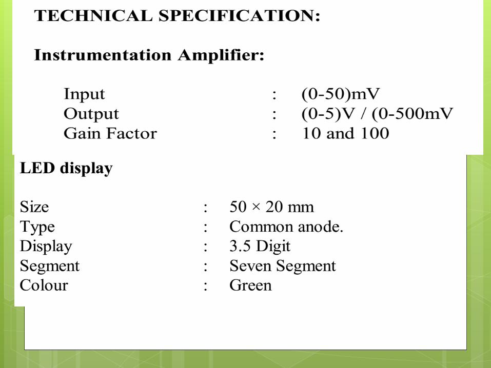
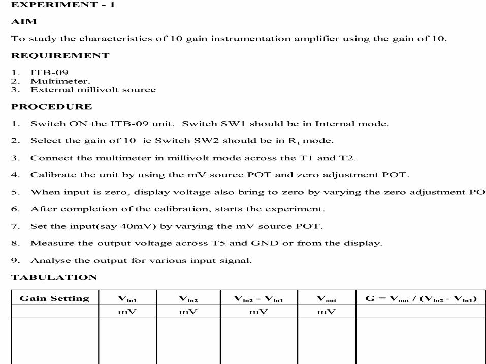
Instrumentation Amplifier


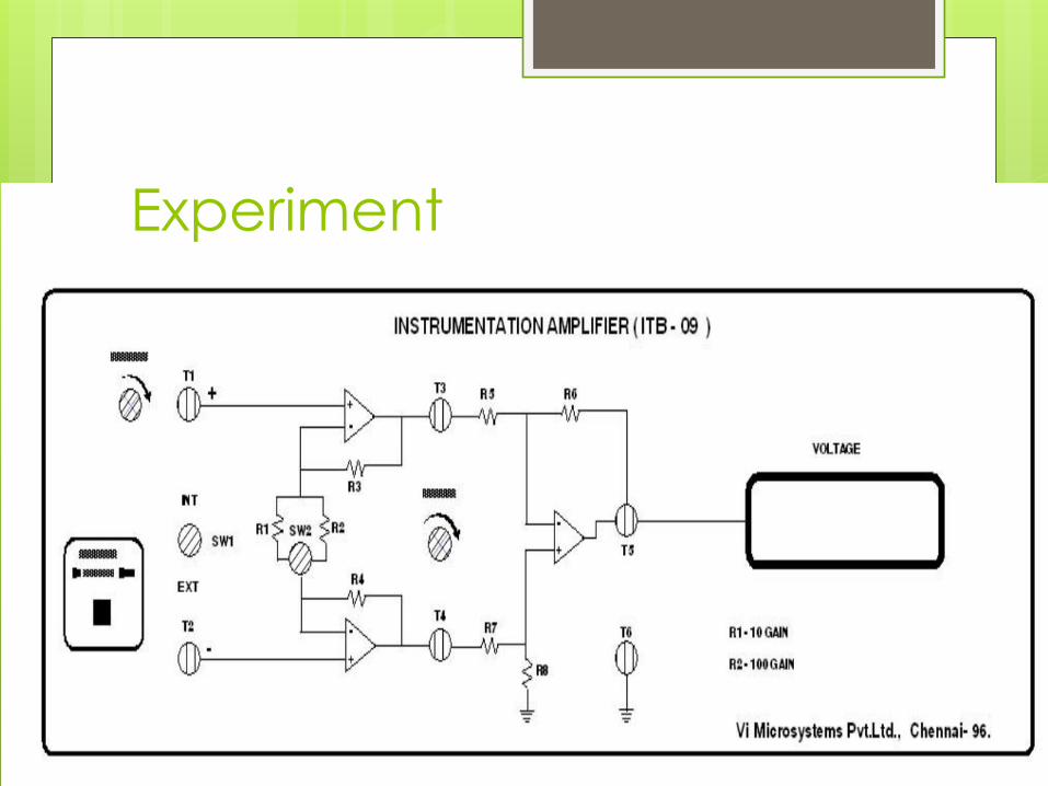
Experiment
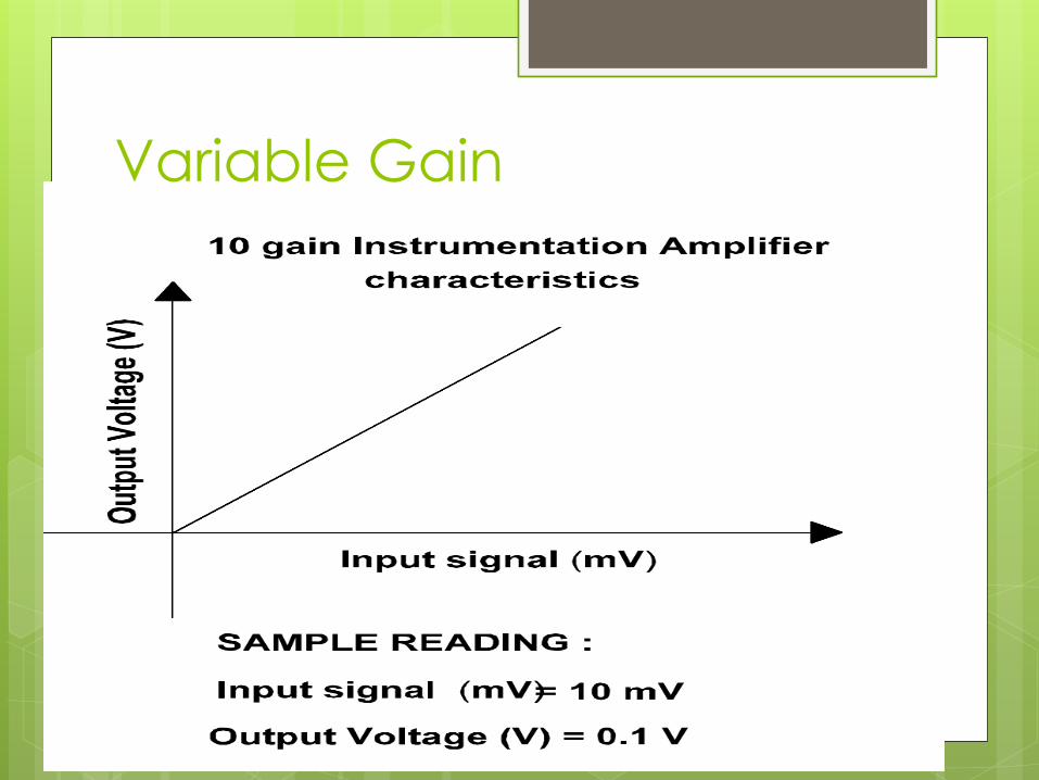
Variable Gain
Instrumentation Amplifiers 69
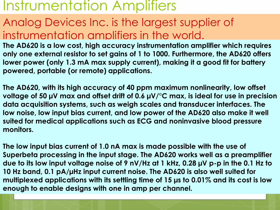
Analog Devices Inc. is the largest supplier of
instrumentation amplifiers in the world. The AD620 is a low cost, high accuracy instrumentation amplifier which requires
only one external resistor to set gains of 1 to 1000. Furthermore, the AD620 offers
lower power (only 1.3 mA max supply current), making it a good fit for battery
powered, portable (or remote) applications.
The AD620, with its high accuracy of 40 ppm maximum nonlinearity, low offset
voltage of 50 µV max and offset drift of 0.6 µV/°C max, is ideal for use in precision
data acquisition systems, such as weigh scales and transducer interfaces. The
low noise, low input bias current, and low power of the AD620 also make it well
suited for medical applications such as ECG and noninvasive blood pressure
monitors.
The low input bias current of 1.0 nA max is made possible with the use of
Superbeta processing in the input stage. The AD620 works well as a preamplifier
due to its low input voltage noise of 9 nV/Hz at 1 kHz, 0.28 µV p-p in the 0.1 Hz to
10 Hz band, 0.1 pA/µHz input current noise. The AD620 is also well suited for
multiplexed applications with its settling time of 15 µs to 0.01% and its cost is low
enough to enable designs with one in amp per channel.

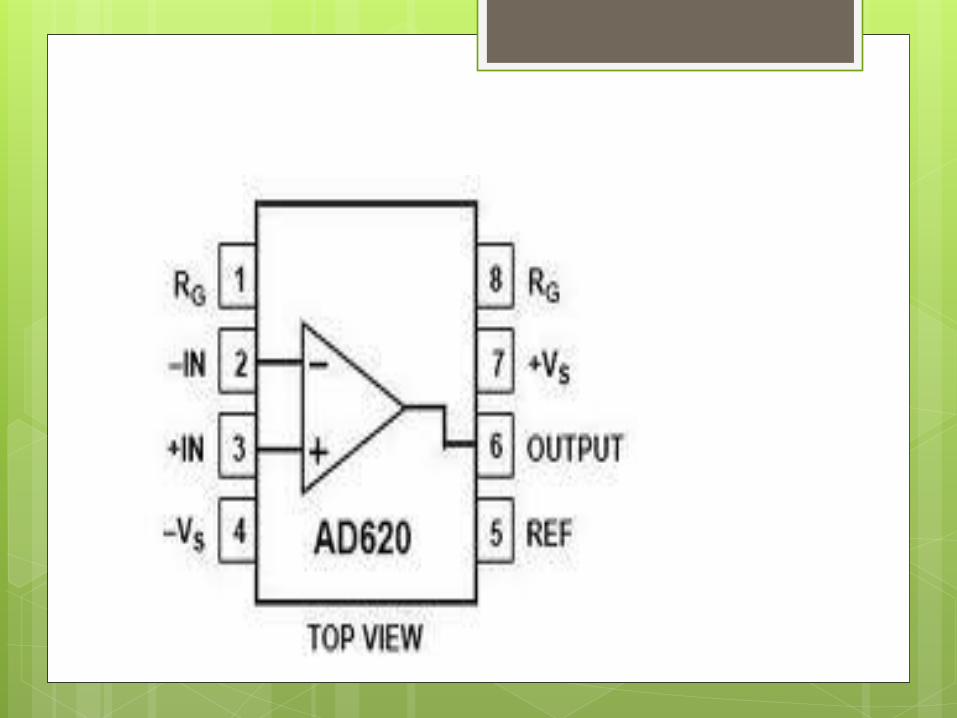
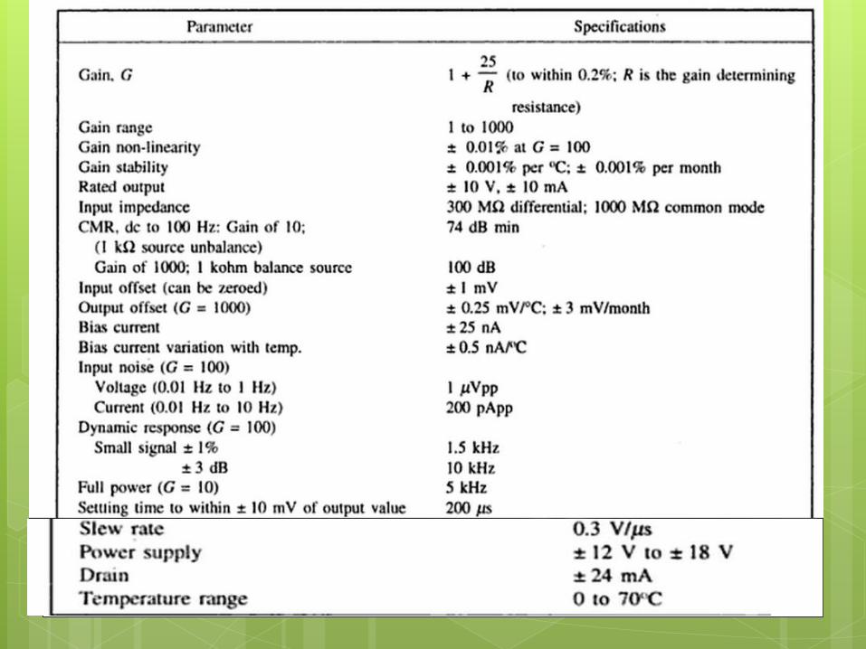
AD620
Specifications
70
http://products.analog.com/products/info.asp?product=AD620
common-mode rejection ratio
(CMRR): The ratio of the
common-mode interference
voltage at the input of a
circuit, to the corresponding
interference voltage at the
output.

Electrostatic Warning for the
AD620 In-Amp
71
AD620 vs opamp
72
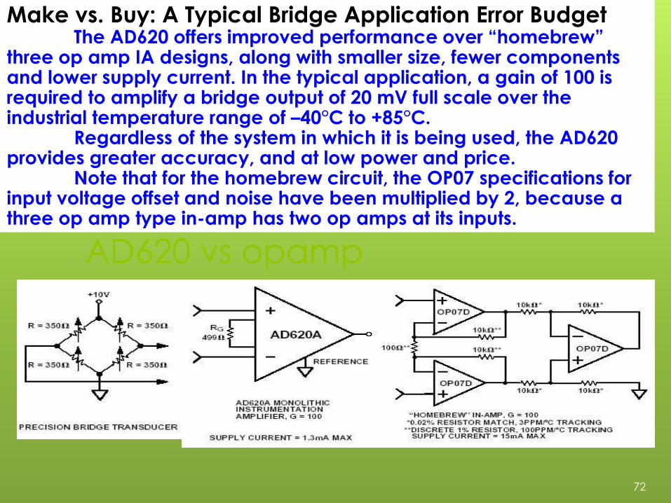
Make vs. Buy: A Typical Bridge Application Error Budget The AD620 offers improved performance over “homebrew” three op amp IA designs, along with smaller size, fewer components and lower supply current. In the typical application, a gain of 100 is required to amplify a bridge output of 20 mV full scale over the industrial temperature range of –40°C to +85°C. Regardless of the system in which it is being used, the AD620 provides greater accuracy, and at low power and price. Note that for the homebrew circuit, the OP07 specifications for input voltage offset and noise have been multiplied by 2, because a three op amp type in-amp has two op amps at its inputs.
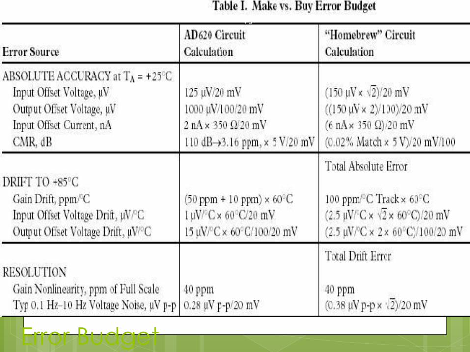
Error Budget
73
Op07 vs LM741
The OP-07 has very low input offset voltage (25µV max for
OP-07A) which is obtained by trimming at the wafer stage.
These low offset voltages generally eliminate any need for external nulling. The OP-07 also features low input bias
current (±2nA for OP-07A) and high open-loop gain
(300V/mV for the OP-07A). The low offsets and high open-
loop gain make the OP-07 particularly useful for high-gain
instrumentation applications.
The wide input voltage range of ±13V minimum combined
with the high CMRR of 110dB (OP-07A) and high input
impedance provides high accuracy in the non-inverting
circuit configuration. Excellent linearity and gain accuracy
can be maintained even at high closed-loop gains.
The OP-07 is available in five standard performance grades.
74
The LM741 series are general purpose operational amplifiers which
feature improved performance over industry standards like the LM709.
They are direct, plug-in replacements for the 709C, LM201, MC1439 and
748 in most applications.
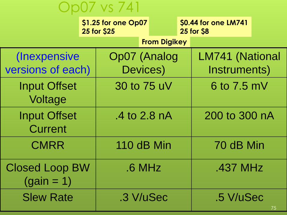
Op07 vs 741
(Inexpensive
versions of each)
Op07 (Analog
Devices)
LM741 (National
Instruments)
Input Offset
Voltage
30 to 75 uV 6 to 7.5 mV
Input Offset
Current
.4 to 2.8 nA 200 to 300 nA
CMRR 110 dB Min 70 dB Min
Closed Loop BW
(gain = 1)
.6 MHz .437 MHz
Slew Rate .3 V/uSec .5 V/uSec 75
$0.44 for one LM741
25 for $8
$1.25 for one Op07
25 for $25
From Digikey


