ISSN: 2455-2631 © May 2021 IJSDR | Volume 6 Issue 5
IJSDR2105025 www.ijsdr.orgInternational Journal of Scientific Development and Research (IJSDR) 145
DESIGN OF ISOLATED HIGH GAIN DC-DC
CONVERTER FOR LOW VOLTAGE INPUT DC SOURCE
1R.Thangapandian, 2C. Maha Lakshmi, 3M.Jothi, 4C.Selvapetchiammal
1Assistant professor, 2Student, 3Student, 4Student
Department of Electrical and Electronics Engineering
P.S.R.Rengasamy college of Engineering for women, Sivakasi, India.
Abstract -This paper presents a resonant converter for dc-dc converter to improve the voltage gain. Here LLC resonant
converter is composed of two capacitors and one resonant inductor. The resonant converter has low switching losses due to
zero voltage switching operation. Due to low switching losses, LLC resonant converter is operate at high switching
frequencies, while maintaining high efficiency. A constant frequency phase shift control scheme between the primary and
secondary controls are designed. Constant frequency switching that equals the resonant frequency of the resonant tank
reduces magnetic simplicity.
Index terms: Resonant converter, Basic dc-dc converter, Voltage conversion ratio.
I. INTRODUCTION
A High gain dc-dc converter is used in many application as interfaces between renewable energy, high voltage DC buses
and grid integration. Buck, Boost, BuckBoost, Cuk, Zeta circuits are the mostly used configurations. It ideally works by adjusting
duty cycle to increase the voltage conversion ratio. These converter can work only within specific range. Normally Transformers,
Coupled inductors, Cascade structures, switch-capacitors and voltage multipliers are used to increase the voltage conversion ratio.
The use of transformer will increase the size and cost of the circuit.
High efficiency and gain can be achieved by providing the method of half bridge current is fed to the converter for
voltage conversion. High efficiency can also be achieved by using the following method of ZVS pulse width modulation.[3]High
efficiency can be achived and losses are to be reduced. By using the method of a step up single switch quadratic buck boost
converter. [5] The voltage gain is achieved in a less time by using the method of “Extended phase shift control of isolated
bidirectional DC-DC converter for power distribution in Microgrid” and it needs auxilary switches for voltage balancing for Zero
Voltage Switching ZVS.[7]By using the method of soft switching implementation the losses are to be reduced. The main
disadvantages is it requires a dual control scheme seperately for primary and secondary controls. By using the method of DC DC
converter design based on the bidirectional switches and galvanic isolation high gain can be achieved.[9]The combination of voltage
multipliers and conventional boost converter can be used to reached the high voltage conversion.[10]
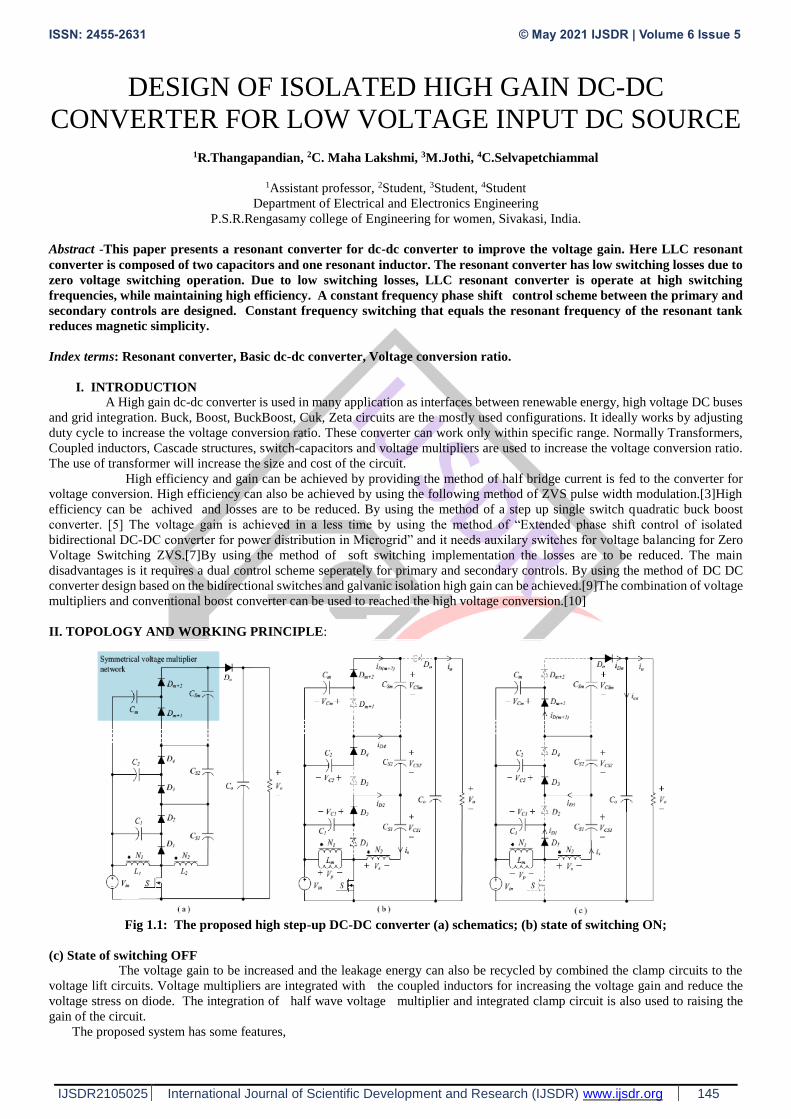
II. TOPOLOGY AND WORKING PRINCIPLE:
Fig 1.1: The proposed high step-up DC-DC converter (a) schematics; (b) state of switching ON;
(c) State of switching OFF
The voltage gain to be increased and the leakage energy can also be recycled by combined the clamp circuits to the
voltage lift circuits. Voltage multipliers are integrated with the coupled inductors for increasing the voltage gain and reduce the
voltage stress on diode. The integration of half wave voltage multiplier and integrated clamp circuit is also used to raising the
gain of the circuit.
The proposed system has some features,
ISSN: 2455-2631 © May 2021 IJSDR | Volume 6 Issue 5
IJSDR2105025 www.ijsdr.orgInternational Journal of Scientific Development and Research (IJSDR) 146
● The system can be controlled by a single switch. So this topology can be easily extended without adding extra
windings for ultra-high step-up conversion ratio.
● Voltage spikes are avoided, and the conversion efficiency is increased by using the lossless clamp circuit in the proposed
system.
SVMN is abbreviated from the symmetrical voltage multiplier networks. It is one of the component of proposed system.
SVMN contains two diodes and two capacitors for achieving high step up conversion ratio.
The voltage across the capacitors can be determined as,
When the power switch is turned on condition
The voltage across the capacitors can be expressed as,
When the power switch is turned off condition
III. DESIGN AND GUIDELINES: A 100KHZ switching frequency is suitable for 40V-60V input 400V/400W- output Prototype. The parameters
of resonant tank Lr and Cr are designed by the main constraints resonant frequency and output power. The DC voltage on the
capacitor is equal to half of the output voltage. The DC voltage is comparatively higher then the maximum voltage ripple. The
value of resonant capacitance is,
Let assume V O=400V, Po=400W and TS=10μs in the above formula, we get Cr >12.5nF
IV. VOLTAGE CONVERSION RATIO: The converter works in two modes namely buck and boost mode. Buck mode for primary phase shift control and
boost mode for secondary phase shift control.The voltage conversion ratio of the proposed converter is,
Mccm=V0/Vin= (3+2nK)/(1-D)
In voltage gain the effect of coupling coefficient is insufficient. Let neglected the leakage inductor and assume k=1,
the ideal transfer relationship can be written as
Mccm =V0/Vin =(3+2n)/(1-D)
The Converter operates in boost mode when the conversion ratio G>1.Here the primary side dφP is constant
and secondary side dφP is used to regulate the output voltage.
The Converter operates in buck moode when the conversion ratio is G<1.Here the primary side dφP is used to
regulate the voltage.
ISSN: 2455-2631 © May 2021 IJSDR | Volume 6 Issue 5
IJSDR2105025 www.ijsdr.orgInternational Journal of Scientific Development and Research (IJSDR) 147
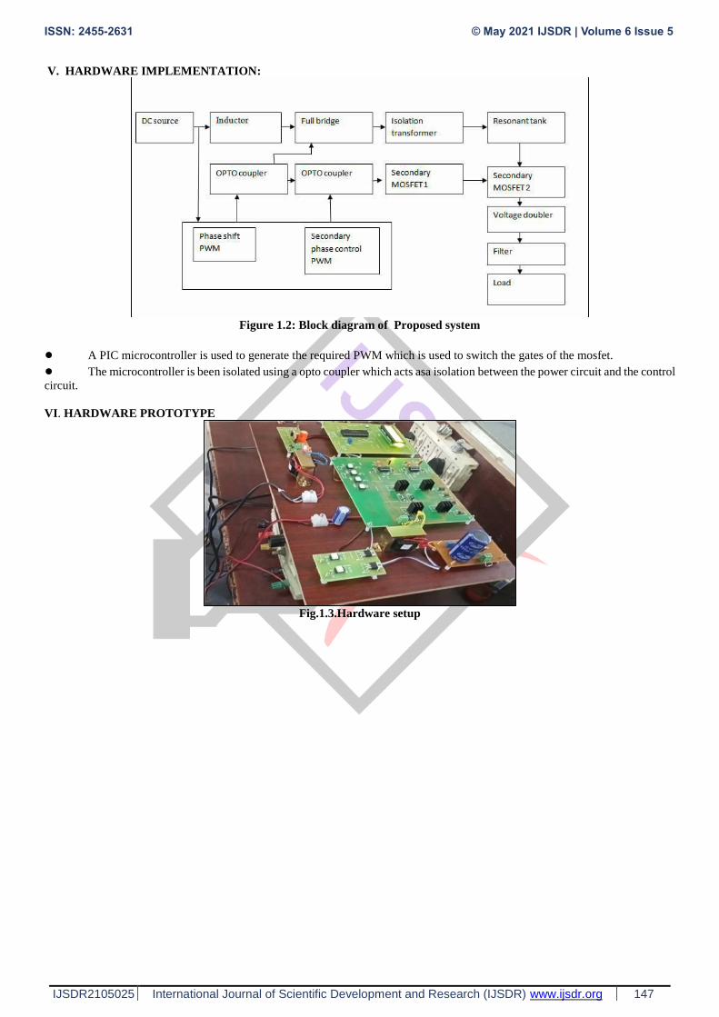
V. HARDWARE IMPLEMENTATION:
Figure 1.2: Block diagram of Proposed system
● A PIC microcontroller is used to generate the required PWM which is used to switch the gates of the mosfet.
● The microcontroller is been isolated using a opto coupler which acts asa isolation between the power circuit and the control
circuit.
VI. HARDWARE PROTOTYPE
Fig.1.3.Hardware setup
ISSN: 2455-2631 © May 2021 IJSDR | Volume 6 Issue 5
IJSDR2105025 www.ijsdr.orgInternational Journal of Scientific Development and Research (IJSDR) 148
VI. EXPERIMENTAL RESULTS:
Figure 1.4: Simulink model of Resonance based High gain converter-open loop
Figure 1.5: Boost mode waveforms
Figure1.6: Input and Output Voltage
The figure 1.5 shows Input and the Output voltage of the converter and PWM driving schemes of the converter.It provides a boost
operation with Vin= 50V and Vout=421V.
ISSN: 2455-2631 © May 2021 IJSDR | Volume 6 Issue 5
IJSDR2105025 www.ijsdr.orgInternational Journal of Scientific Development and Research (IJSDR) 149
Figure 1.7: PWM signal for switches
The primary side switches S1 & S4 operates with a duty of 50% whereas S2 & S3 operates with phase shift control of 1µs with
30% duty. The secondary side switches operates with 45% duty.
Figure1.8: Resonant state waveforms
Figure 1.9: Soft switching waveforms of the switches S1 and S6
ISSN: 2455-2631 © May 2021 IJSDR | Volume 6 Issue 5
IJSDR2105025 www.ijsdr.orgInternational Journal of Scientific Development and Research (IJSDR) 150
Figure 1.10: Proposed system Efficiency
CONCLUSION
To achieve a high efficiency for low voltage input dc sources the resonant converters with constant-frequency phase-shift control
is proposed in this paper. The Design of the resonant converters with constant-frequency phase-shift control are designed to
achieve high efficiency over a wide operating range for applications such as the converter provides efficiency over a range , With
the enhanced efficiency and high power control this converter can be applied to low voltage input dc-dc conversions.
REFERENCES [1] L. S. Yang, T. J. Liang, H. C. Lee, and J. F. Chen, “Novel high step-up DC–DC converter with coupled- inductor and voltage-
doubler circuits,” IEEE Trans. Ind. Electron., vol. 58, no. 9, pp. 4196–4206, Sep. 2011.
[2] J.Zhang,F,Zhang, “A novel ZVS DC/DC Converter for high power Applications” ,IEEE power electronics,2017.
[3] S. K. Changchien, T. J. Liang, J. F. Chen, and L. S. Yang, “Novel high step-up DC–DC converter for fuel cell energy conversion
system”,IEEE Trans. Ind. Electron., vol. 57, no.
6, pp. 2007–2017, Jun. 2010.
[4] Y. P. Hsieh, J. F. Chen, T. J. Liang, and L. S. Yang, “A novel high step-up DC–DC converter for a Microgrid system”, IEEE
Trans. Power Electron., vol. 26, no. 4, pp. 1127–1136, Apr. 2011.
[5] Zhang,n. Zhang. G.,See.K.W. and Zhang,B,2017“A single switch quadratic buck boost converter with continuous input port
current and continuous output port current
[6] W. Li, Y. Zhao, J. Wu, and X. He, “Interleaved high step-up converter with winding cross coupled inductors and voltage
multiplier cells,”IEEE Trans. Power Electron., vol. 27, no. 1, pp. 133–143, Jan. 2012.
[7] B.Zhao,Q.Yu,W.sun, “ Extended phase shift control of isolated bidirectional DC-DC converter for power distribution in
Microgrid” IEEE power electronics,2017
[8] G. A. L. Henn, R. N. A. L. Silva, P. P. Praca, L. H. S. C. Barreto, and D. S. Oliveira, Jr., “Interleaved-boost converter with
high voltage gain,” IEEE Trans. Power Electron., vol. 25, no.11, pp. 2753–2761, Nov. 2010.
[9] W. Li, Y. Zhao, Y. Deng, and X. He, “Interleaved converter with voltage multiplier cell for high step-up and high efficiency
conversion,”IEEE Trans. Power Electron., vol. 25, no. 9, pp. 2397– 2408, Sep. 2010.
[10] L.Muller and J.W.Kimball ,”High gain DC DC Converter based on the cockraft-Walton multiplier ”IEEE
Trans.powerelectron..vol.23,no2,pp,871-887.Mar.2008
[11]Y. Ren. M. Xu, J. Sun. F. C. Lee, "A family of high power density unregulated bus converters," IEEE Trans. Power Electron.,
vol. 20, no. 5,pp. 1045-1054, Sep. 2006.
[12] H. Wu, Y. Xing, "Families of forward converters suitable for wide input voltage range applications," IEEE Trans. Power
Electron., vol. 29, no. 11, pp. 6006-6017, Nov. 2014