25
Ashutosh Tiwari Design of MOS Amplifiers Using gm/ID Methodology

Ashutosh Tiwari
Design of MOS Amplifiers Using gm/ID Methodology
Ashutosh Tiwari
Outline
IntroductionWhy gm/Id MethodologyPerformance MetricsGeneration Of Performance CurvesImplementation And Design examples
Ashutosh Tiwari
Introduction
Mainstream methods assume generally strong inversion and use the transistor gate voltage overdrive (Vov) as the key parameterMicropower design techniques, on the other hand, exploit weak inversion models.This methodology is based on a unified synthesis methodology in all the regions of operation of MOS transistor.

Ashutosh Tiwari
Introduction
The method exploits the transconductanceover dc drain current ratio (gm/Id) relationship versus the normalized current [Id/(W/L)].

Ashutosh Tiwari
Why gm/Id Methodology
Consider a simple common source amplifier, the power and bandwidth are given by following equations:
Ashutosh Tiwari
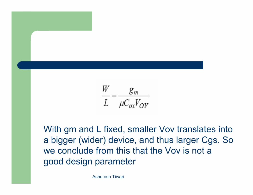
With gm and L fixed, smaller Vov translates into a bigger (wider) device, and thus larger Cgs. So we conclude from this that the Vov is not a good design parameter

Ashutosh Tiwari
Why gm/Id Methodology
The choice of gm/Id is based on its relevance for the three following reasons:1. It is strongly related to the performances of
analog circuits. 2. It gives an indication of device operating
region.3. It provides a tool for calculating the
transistors dimensions.

Ashutosh Tiwari
How gm/Id is an indicator of the mode of operation?
This derivative is maximum in weak inversion region. The gm/Id ratio decreases as the operating point moves toward strong inversion.

Ashutosh Tiwari
What we really want from MOS transistor– Large gm without investing much current– Large gm without having large Cgs
To quantify how good of a job our transistor does, we can therefore define the following "figures of merit”:

Ashutosh Tiwari
Performance Metrics of Interest:
Transit Frequency: (or Unity Gain Frequency)
It is the maximum frequency beyond which MOS transistor will not act as amplifier.
Intrinsic Gain:
Ashutosh Tiwari
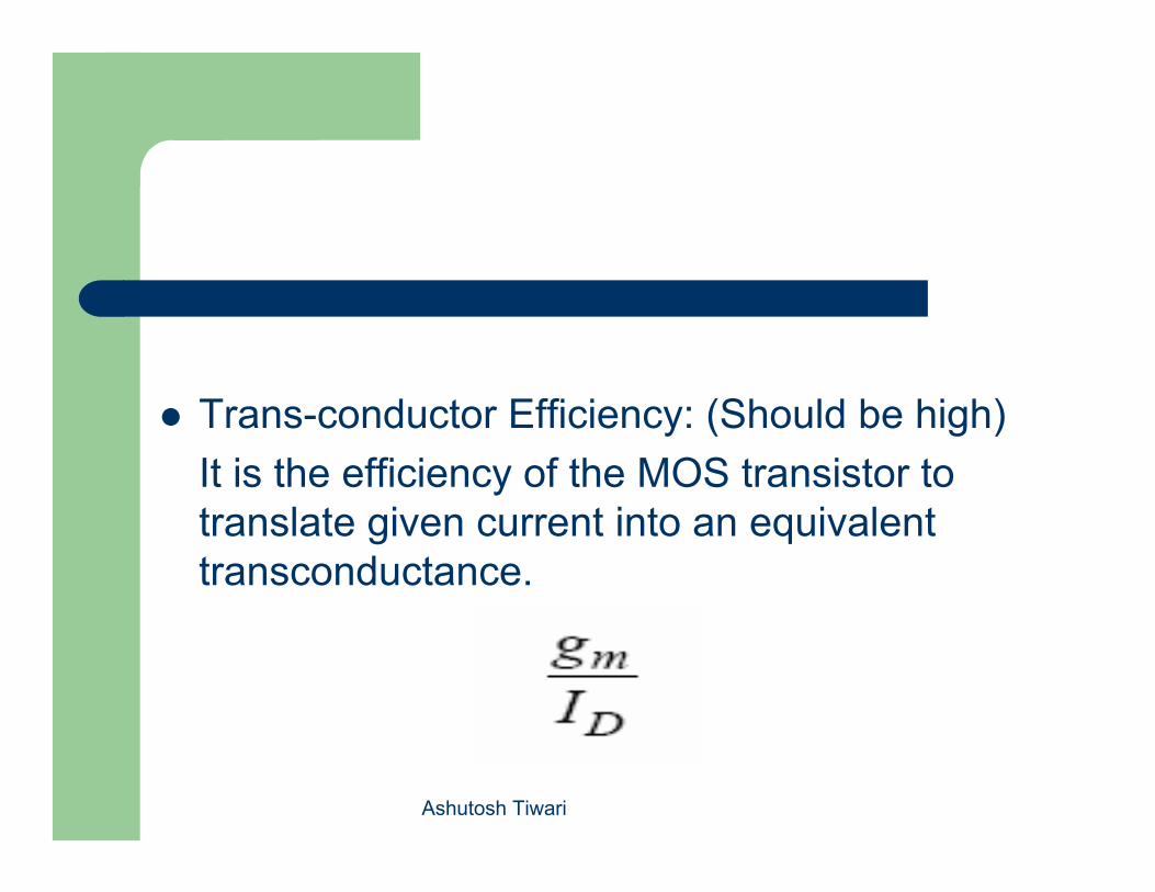
Trans-conductor Efficiency: (Should be high)It is the efficiency of the MOS transistor to translate given current into an equivalent transconductance.

Ashutosh Tiwari
Generation of Performance Curves
gm/ID Simulation

Ashutosh Tiwari
gm/ID Vs Vov curve

Ashutosh Tiwari
Ashutosh Tiwari
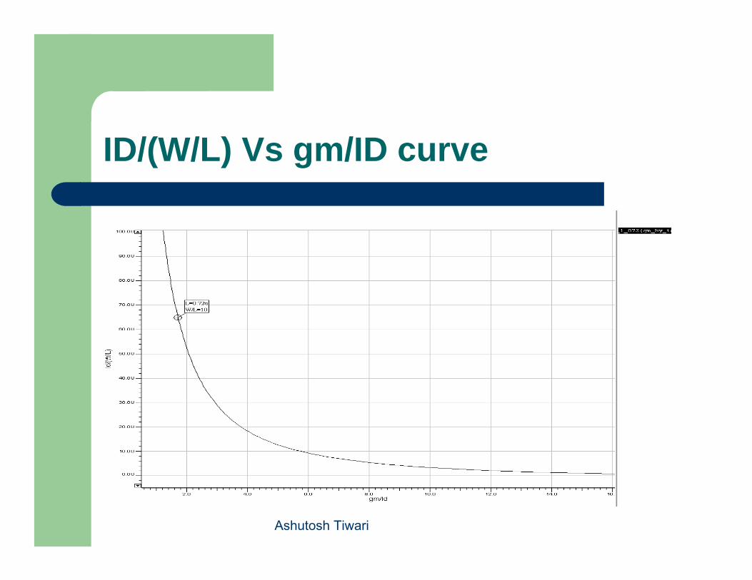
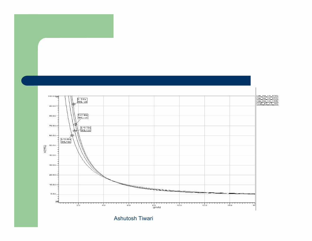
ID/(W/L) Vs gm/ID curve
Ashutosh Tiwari
Ashutosh Tiwari
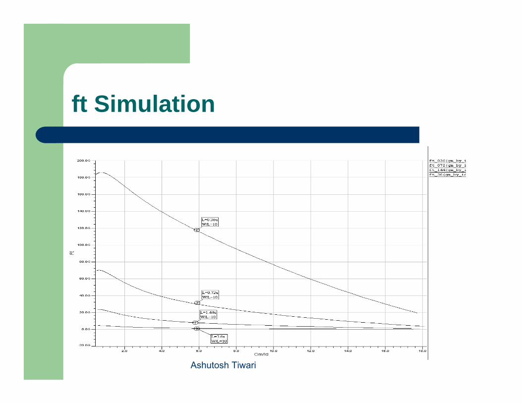
ft Simulation

Ashutosh Tiwari
Intrinsic Gain Simulation

Ashutosh Tiwari
Gm×ro Vs Vds Curve

Ashutosh Tiwari
Design Example:
Given specifications
– DC gain=-2, ID ≤ 1mA, f-3dB=100MHz, CL=10pF

Ashutosh Tiwari
Solution:− From the given specifications, we can find gm and RL as
follows:
Ashutosh Tiwari
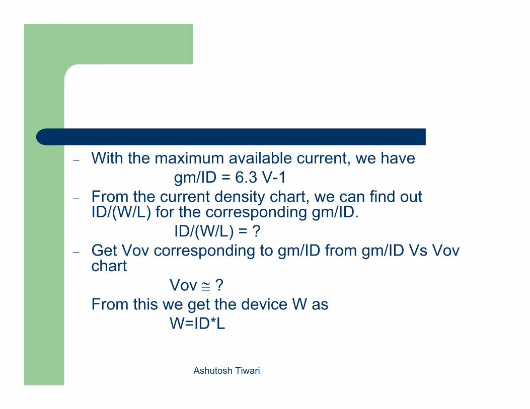
− With the maximum available current, we havegm/ID = 6.3 V-1
− From the current density chart, we can find out ID/(W/L) for the corresponding gm/ID.
ID/(W/L) = ? − Get Vov corresponding to gm/ID from gm/ID Vs Vov
chart Vov ≅ ?
From this we get the device W as W=ID*L

Ashutosh Tiwari
Design Example:Differential Amplifier (Single Ended Output)

Ashutosh Tiwari
Thank You?
Ashutosh Tiwari
References
D. Flandre, A. Viviani, J.-P. Eggermont, P. Jespers, "Improved synthesis of regulated-cascode gain-boosting CMOS stage using symbolic analysis and gm/ID methodology", IEEE Journal of Solid-State Circuits (Special Issue on 22nd ESSCIRC conference), 32 (1997) 1006-1012.Silveira F., Flandre D., Jespers P.G.A. A gm/ID based methodology for the design of CMOS analog circuits and its application to the synthesis of a silicon-ion- insulator micropower OTA. IEEE Journal of Solid State Circuits. Vol. 31, pg 1314-1319, Sept. 1996.


