Design of Multi-bit Sigma-Delta Modulators for Digital Wireless Communications Bingxin Li Stockholm, 2003 Submitted to KTH, Royal Institute of Technology, in partial fulfillment of the requirements for the degree of Doctor of Technology.
Transcript
Design of Multi-bit Sigma-Delta Modulators
for Digital Wireless Communications
Bingxin Li
Stockholm, 2003
Submitted to KTH, Royal Institute of Technology, in partial fulfillment of therequirements for the degree of Doctor of Technology.
Bingxin Li
Design of Multi-bit Sigma Delta Modulators for Digital Wireless Communications
ISBN 91-7283-641-5ISRN KTH/IMIT/LECS/AVH-03/10--SEISSN 1651-4076TRITA-IMIT-LECS AVH 03:10
Copyright 2003, by Bingxin Li
Kungl Tekniska Högskolan / Royal Institute of TechnologyDepartment of Microelectronics & Information TechnologyLaboratory of Electronics and Computer SystemsElectrum 229SE-164 40 KistaSweden
The ever advance of CMOS digital circuit process leads to the trend of digitizing ananalog signal and performing digital signal processing as early as possible in a signalprocessing system, which in turn leads to an increasing requirement on analog-to-dig-ital converter (ADC). A wireless transceiver is a such kind of signal processing sys-tem. Conventional transceivers manipulate (filter, amplify and mix) the signal mostlyin analog domain. Since analog filters are difficult to design on-chip, the system inte-gration level is low. Modern transceivers shift many of these tasks to digital domain,where the filtering and channel selection can be realized more accurately and morecompactly. However the price for the high integration level is the critical requirementon the ADC, because the simplified analog part sends not only the weak signal but alsothe unwanted strong neighboring channel to the ADC. In order to digitize the neededsignal in the presence of strong disturbances, a high dynamic-range and high-speedADC is needed.
Sigma Delta ADCs are promising candidates for A/D conversion in modern wirelesstransceivers. They are naturally suitable for high-resolution narrow-band A/D conver-sions. With the development of processing and design techniques, sigma delta ADCsare expanding their applications to moderate-band area, such as wireless communica-tion baseband processing. Currently mobile communication systems are migratingfrom 2G to 3G. In 2G systems the baseband width is in the order of hundred kHz,while in 3G systems the baseband width is in the order of MHz. To face the challengeof designing a high resolution sigma delta ADC with large bandwidth, a multi-bit in-ternal quantizer is often used. In this thesis special design considerations on multi-bitsigma delta modulators are discussed. The biggest drawback of multi-bit sigma deltamodulators is the need of an extra circuit to attenuate or compensate the internal multi-bit DAC non-linearity. This thesis provides a comprehensive analysis of the solutionwhich combines a multi-bit quantizer with a 1-bit DAC in a sigma delta modulator.The theoretical analysis result is verified by measurement results. Another topic ad-dressed in the thesis is how to reduce the multi-bit quantizer complexity. It is shownthat by using a semi-uniform quantizer, the quantizer can reduce its complexity byone-bit yet still maintain the same modulator dynamic range. The performance of thesemi-uniform quantizer is also verified by measurement results.
ii
iii
Acknowledgments
First I would like to thank my supervisor Professor Hannu Tenhunen for accepting meas a doctoral student in the Electronic System Design Laboratory (now LECS Lab).During all these years he has not only tought me on the subjects that I was working on,but also expanded my vision on the development of microelectronics science. It is apleasant experience to study in the ESD Lab, which has a free and active atmosphere.
Thanks to Lena Beronius for all the excellent administrative work done for us. And alsomany thanks to Hans Berggren, Julio Mercado, Richard Andersson, and Peter Magnus-son for maintaining a robust computer network and installing all the useful software forus.
Many thanks to all the nice and helpful colleagues Lirong Zheng, Li Li, AndreasGöthenberg, Johnny Öberg, Mikael Millberg, Xingzhong Duo, Meigen Shen, Zhong-hai Lu, Yiran Sun and many others. The discussions with them broaden my knowledgeand stimulate new ideas. Special thanks to Steffen Albrecht, Adam Strak, and AnaRusu for their helpful comments to the thesis draft.
The author would like to thank Professor Mohammed Ismail, Professor Håkan Olsson,and Dr. Xiaopeng Li. It was a pleasant collaboration with them in the design work ofa multi-standard sigma delta modulator chip. Also many thanks to Gang Xu in LundUniversity for the helpful discussions.
The author would like to thank Xing Liu and Roshan Weerasekera for their help in lay-out design of two chips.
Finally I would like to express sincere gratitude to my wife and my daughters. It is thiswarm family that supports me finishing my study during the years. I would also takethe chance to thank my parents and my sister, for their love and support to me.
Bingxin Li Stockholm, 2003
iv
v
List of publication
Papers included in this thesis:
(1) Bingxin Li and Hannu Tenhunen, “A second order multi-bit sigma delta modulatorwith single-bit feedback”, Journal of Analog Integrated Circuits and Signal Process-ing, vol. 38, issue 1, pp. 63-72, January 2004.
(2) Bingxin Li and Hannu Tenhunen, "Design of semi-uniform qauntizers and their appli-cation in sigma delta A/D converters", to appear in Journal of Analog Integrated Cir-cuits and Signal Processing, 2004.
(3) Bingxin Li and Hannu Tenhunen, "A structure of cascading multi-bit modulatorswithout dynamic element matching or digital correction", in proc. of 2002 Interna-tional Symposium on Circuits and Systems, pp. III 711-714, Phoenix, May 2002.
(4) Bingxin Li and Hannu Tenhunen, "Sigma delta modulators using semi-uniform quan-tizers", in proc. of 2001 International Symposium on Circuits and Systems, pp. I 456-459, Sydney, May 2001.
(5) Bingxin Li, Lirong Zheng, and Hannu Tenhunen, "An improved settling model ofswitched-capacitor integrator for high speed sigma-delta modulator simulation", inproc. of 2000 IEEJ International Analog VLSI Workshop, pp. 47-50, Stockholm, June2000.
(6) Bingxin Li, Lirong Zheng, and Hannu Tenhunen, "A design of operational amplifierfor sigma delta modulators using 0.35um cmos process", in proc. Tenth InternationalConference on Very Large Scale Integration, pp. 23-34, Lisboa, December 1999.
(8) Bingxin Li, and Hannu Tenhunen, "A 2MS/s Second Order 5-bit Sigma Delta Modu-lator Using Single-bit DAC", submitted to IEEE Transaction of Circuits and SystemsII: Analog&Digital Signal Processing, 2003.
vi
Other publications
(9) Bingxin Li and Hannu Tenhunen, "A second order sigma delta modulator using semi-uniform quantizer with 81db dynamic range at 32x OSR", in proc. of 2002 EuropreanSolide States Circuits Conference, pp. 579-582, Florence, September 2002.
(10) Bingxin Li and Hannu Tenhunen, "A second order multi-bit sigma delta modulatorwith single-bit feedback", in proc. of 20th Norchip Conference, pp. 241-246, Copen-hagen, November 2002.
(11) Bingxin Li and Hannu Tenhunen, "Signal scaling in multi-bit sigma delta modula-tors", in proc. of 19th Norchip Conference, pp. 204-209, Stockholm, November 2001.
med Ismail, and Hannu Tenhunen, "A Dual-Standard GSM/DECT Baseband Sigma-Delta ADC", in proc. of 18th Norchip Conference, pp. 326-331, Turku, Finland,November 2000.
(13) Sascha Thoss, Bingxin Li, and Hannu Tenhunen, "Loop coefficieny optimization forcascaded sigma delta modulators - a case study", in proc. of 2000 IEEJ InternationalAnalog VLSI Workshop, pp. 51-56, Stockholm, June 2000.
(14) Steffen Albrecht, Bingxin Li, Costantino Pala, Xiaopeng Li, Mohammed Ismail, and
Hannu Tenhunen, "A Sigma-Delta A/D based architecture for Multi-Standard Front-End radio receivers", in proc. of IEEJ International Analog VLSI Workshop, pages37-42, Stockholm, Sweden, June 2000.
(15) L.-R. Zheng, B. X. Li, and H. Tenhunen, "Efficient and accurate modeling of powersupply noise on distributed on-chip power networks", in proc. IEEE InternationalSymposium on Circuit and Systems, pp. II 513-516, Geneva, Switzerland, 2000.
(16) Bingxin Li and Hannu Tenhunen, "Modeling some second-order non-idealities in highorder sigma delta modulators", in proc. of 17th Norchip Conference, pp. 152-157,Oslo, November 1999.
(17) Bingxin Li, Lirong Zheng, and Hannu Tenhunen, "Hierarchical modeling of sigmaldelta modulators for noise coupling analysis",in proc. of 1999 Southwest Symposiumon Mixed-Signal Design, pp. 58-62, Tucson, April 1999.
(18) Andreas Gothenberg, Bingxin Li, and Hannu Tenhunen, "A method for stability andperformance analysis of low oversampling ratio higher order sigma delta noise shaperarchitectures", in proc. Midwest Symposium on Circuits and Systems, Las Cruces,NM, U.S.A., Aug 1999.
vii
(19) Lirong Zheng, Bingxin Li, and Hannu Tenhunen, "Global interconnect design for highspeed ULSI and system-on-package", in proc. of the 12th Annual IEEE InternationalASIC/SOC Conference, pp. 251-280, Washington, DC, USA, Sep 1999.
(20) Bingxin Li, Lihong Jia, and Hannu Tenhunen, "Optimization of analog modeling and
simulation", in proc. of 5th International Conference on Solid-State and IntegratedCircuit Technology, pp. 385-388, Beijing, October 1998.
(21) Lihong Jia, Bingxin Li, and Hannu Tenhunen, "Implementation of a low-power 128-point FFT", in proc. of 5th International Conference on Solid-State and Integrated Cir-cuit Technology, pp. 369-372, Beijing, October 1998.
(22) Bingxin Li, Design of Sigma Delta Modulators for Digital Wireless Communications,Licentiate of Technology thesis, 2001, ISSN 1104-8697. ISRN KTH/ESD/AVH-2001/2-SE.
viii
Contents
Abstract ............................................................................................................ iAcknowledgement ............................................................................................ iiiList of Publications .......................................................................................... vContents ........................................................................................................... viiiList of abbreviations ........................................................................................ x
Chapter 1 Introduction ............................................................................... 1 1.1 Thesis background ............................................................................................. 1 1.1.1 Background ............................................................................................. 1 1.1.2 Recent development ................................................................................ 3 1.2 Motivation .......................................................................................................... 5 1.2.1 Problem statement ................................................................................... 5 1.2.2 Solutions ................................................................................................. 5 1.2.3 Increase of sampling frequency .............................................................. 5 1.2.4 Increase of noise-shaping order .............................................................. 6 1.2.5 Thesis focus - increase of quantizer resolution ....................................... 7 1.3 Thesis outline ..................................................................................................... 9
Though our world has an analog nature, nowadays information is very often stored,transferred, and processed digitally. The advantage is obvious: 1. digital signals aremuch more immune to noise than their analog counterparts. Noise and distortion willaccumulate during the transfer or copy of an analog signal, while a digital signal canbe losslessly copied or transferred as long as the noise and distortion are lower thanthe threshold which changes the digital value. 2. signal processing circuits can be im-plemented more easily, accurately and economically in digital domain thanks to thefast and continuous development of CMOS process. According to ITRS roadmap (In-ternational Technology Roadmap for Semiconductors), the mainstream CMOS pro-cess feature size will be scaled down to 32nm in the next 10 years, which is about onethird of the current technology level (100nm, year 2003).
Fig 1.1 Sampling and quantization
As a result, analog to digital converters (ADC) and digital to analog converters (DAC)are needed to link the analog and digital domains. Information is first converted fromanalog to digital format, processed digitally, and then changed back to analog formatagain if required by the end user of the information. A digital signal is discrete in bothamplitude and time, while an analog signal is continuous in both amplitude and time.Thus an A/D conversion includes two procedures as shown in Fig 1.1: sampling,which makes the signal discrete in time, and quantization, which makes the signal dis-crete in amplitude. Accordingly there are two important specifications for an ADC:speed and resolution. The speed represents how fast the discretization in time can bedone. The resolution represents how accurate the discretization in amplitude can bedone. ENOB (Effective Number of Bit) is often used to characterize the conversion
0001
1011
anal
og a
mpl
itud
e
discretization in time discretization in amplitude
1. Introduction2
resolution.
According to Shannon’s sampling theorem [Sha49], a band-limited analog signal mustbe sampled at least twice of its highest frequency component so that the signal can bereconstructed without loss. Many ADCs are designed to sample the signal just a littlefaster than the Nyquist frequency. These ADCs can be categorized as Nyquist-rateADCs. They can operate at very high speed, resulting in a large bandwidth. Using astandard CMOS process, the conversion bandwidth is expanded to the range of GigaHz [Pou02]. The main drawback of Nyquist-rate ADCs is their low resolution, whichis limited by the matching of analog components. Practically 12~14 bit resolution canbe economically (no calibration or trimming) achieved using Nyquist-rate ADCs[Pan00, Che01]. Another problem is the complex hardware structure. For a flash struc-ture ADC, the hardware complexity (mainly contributed by the large number of com-parators) exponentially increases with the resolution-in-bit. Using other structures likepipeline or folding can reduce the required number of comparators, which is howeverstill large.
Developed in the 60’s of last century [Ino62], Sigma Delta ADCs provide a robust andeconomical solution for high-resolution analog-to-digital conversion. Sigma Deltamodulator is one kind of the so-called error feedback coder, meaning that the coarsequantization error is fed-back to the input. Many varieties of error feedback codershave been proposed in the last century. Although mathematically they all lead to ahigh-resolution, the practical implementation complexity is largely different. For ex-ample a Delta modulator [Jag52] realizes the same noise transfer function as a SigmaDelta modulator, but there the input signal is also filtered by the loop in the same wayas the quantization error. In order to reconstruct the signal an extra inverse loop filteris needed. A Sigma Delta modulator arranges the loop filter in a way that the input sig-nal and the quantization error see different transfer functions. The quantization errorgoes through a first order or higher order difference, yet the input signal is simply de-layed. Theoretically the conversion resolution can be arbitrarily increased until thephysical limitation of device thermal noise floor is reached. The high resolution isachieved through a feedback loop from the digitized output to the modulator input.Since there is a large gain in the forward path of the loop, the long-term average of thedigitized output is forced to be very close to the modulator input. Furthermore, a Sig-ma Delta ADC does not require accurate analog component matching to achieve thesuperior resolution, which makes it suitable for standard CMOS processes. Sigma Del-ta ADCs have to operate at much higher frequency (oversampling) than the Nyquistfrequency, therefore their main drawback is the narrow conversion bandwidth. Com-pared with the Giga Hz range of Nyquist-rate ADCs, Sigma Delta ADCs are currentlycapable of converting a signal within the range of Mega Hz [Kuo02], [Vel03].
With respect to circuit realization, Sigma Delta ADCs can be categorized into discrete-time structure and continuous-time structure. Using switched-capacitor (SC) circuits,discrete-time Sigma Delta ADCs can achieve very high resolution. But the circuit
Thesis background 3
speed is limited by the settling of switched-capacitor integrators. The future advancedCMOS process requires an ultra low supply voltage, which makes the realization ofSC circuit more difficult. On the other hand continuous-time ADCs are more adaptiveto low supply voltage. Input-signal sampling errors, like settling error and charge in-jection, and some other discrete-time problems do not exist in continuous-time cir-cuits. The circuit can operate at a higher speed than its switched-capacitor counterpart.The drawback of continuous-time Sigma Delta ADCs is their sensitivity to clock jitter,which lowers the conversion resolution. But since the requirement on ADC resolutionin wireless receivers is normally lower than applications like digital audio, this draw-back does not prevent continuous-time Sigma Delta ADCs from being a good choicefor receiver baseband conversion.
With respect to conversion signal-band, Sigma Delta ADCs can be categorized intolow-pass ADCs and band-pass ADCs. Band-pass ADCs are especially suitable forconverting a narrow-band signal which has a non-zero centre frequency. This charac-ter makes band-pass ADCs ideal for IF digitization in wireless communications. Re-cently many band-pass ADCs [Sal01], [Sch02] adopt the continuous-time structure toachieve a high centre frequency and large oversampling ratio, where the resolution re-quirement is moderate.
A complete Sigma Delta ADC includes a modulator (mostly analog) and a digital dec-imation filter. The modulator shapes the quantization error and the decimation filterreconstructs the signal in digital form. The focus of this thesis is on the modulator part.
1.1.2 Recent development
Fig 1.2 shows the performance increase of Sigma Delta ADCs in the past 16 years(1988-2003). Those chips that have the highest figure of merit (FOM) of the year areplotted. The FOM is calculated according to the formula:
where ENOB is the effective number of bits, calculated according to the peak signal-to-noise-and-distortion-ratio (SNDR):
From Fig 1.2 it can be seen that in the past 16 years the FOM of Sigma Delta ADCshas increased by more than two order of magnitude. The performance is doubledroughly every two years. A detailed look shows that the achieved conversion resolu-tion has not changed much. Already in the early 90's there was a 20-bit-resolution con-verter reported [Yam94]. It is the continuous increase of signal bandwidth and the
decrease of power consumption that boost the FOM. For example, compare the chipof 1988 and 2003, [Nor88] chip has a 13-bit resolution, while the [Vel03] chip onlyhas 12-bit resolution. But the signal band of [Vel03] chip is 48 times as large as thatof [Nor88] chip, and its power consumption is 1/16 of that of [Nor88] chip. The in-crease of conversion bandwidth and the decrease of power are two contradictory de-sign targets. The simultaneous fulfillment of these two targets is a result of advance inprocess technology and new circuit topology. The [Nor88] chip is designed using1.75µm CMOS process, and the [Vel03] chip is in 0.18µm CMOS process, which is10 times smaller. When the process feature size is scaled down, the gate oxide thick-ness is also scaled down, leading to a larger gate capacitance Cox. According to theequation (NMOS in saturation mode)
With a fixed biasing current, using a smaller feature size process can provide a largergm, and in turn a higher speed. However not everything associated with the technologyscale-down is favorable to analog circuits: 1. the thinner gate oxide layer requires alower supply voltage to keep the electrical field strength constant. Many conventionalcircuit topologies are not suitable to work under such a low supply voltage. The circuitperformance is often sacrificed. 2. the influence of short channel effect is more critical,and 3. the CMOS process parameters are often optimized to meet the requirement ofdigital circuits.
Fig 1.2 Sigma Delta ADC FOM
gm 2µnCoxWL-----ID= (1.3)
[Vel
03]
[Vel
02]
[Oli0
1]
[Cao
00]
[Bre
99]
[Pel
98]
[Rab
97]
[Che
96]
[Bai
95]
[Yin
94]
[Yin
93]
[Ing9
2]
[Bra
91]
[Bra
90]
[Reb
89]
[Nor
88]
1,00E+10
1,00E+11
1,00E+12
1,00E+13
1988
1989
1990
1991
1992
1993
1994
1995
1996
1997
1998
1999
2000
2001
2002
2003
fitting curve
Motivation 5
1.2 Motivation
1.2.1 Problem statement
Sigma Delta ADCs are inherently suitable for high-resolution narrow-band A/D con-versions. Therefore Sigma Delta ADCs find their best application in the areas like dig-ital audios [Bra91, Rit94, Fuj97] or instrument measurements [Yam94]. In modernwireless communication standards, the channel bandwidth is often in the order of hun-dreds of KHz (e.g. GSM, DECT), or even MHz (e.g. UMTS). Furthermore, it is oftenpreferred in modern receivers to directly digitize the IF signal [Sen98], [Sal01] whichranges from tens of MHz to hundreds of MHz. Working at such a high frequency andachieving a high resolution and a low power is a critical challenge for even experi-enced designers.
1.2.2 Solutions
In order to achieve both a large bandwidth and a high resolution, one should increasethe sampling frequency, the noise-shaping order, and the quantizer resolution separate-ly or combined. This can be illustrated in the following equations.
With an ideal noise transfer function (1-z-1)n, the maximum achievable SNR is:
where m is quantizer resolution in bit, k is noise shaping order, and OSR is oversam-pling ratio. Replacing OSR by fs/2fb, where fs is sampling frequency and fb is signalbandwidth, we get:
The product of SNR and fb2k+1 is a constant defined by m, k, and fs. That means with
a fixed noise-shaping order, quantizer resolution, and sampling frequency, there is al-ways a trade-off between the achievable resolution SNR and signal bandwidth fb. Inorder to increase both the SNR and fb simultaneously, a larger m, k, and fs have to beused separately or combined. These three methods are briefly discussed below.
1.2.3 Increase of sampling frequency
In a switched-capacitor realization of Sigma Delta ADCs, the sampling frequency is
SNR32--- 2
m1–( )
2
π2k----------------------- 2k 1+( )OSR
2k 1+= (1.4)
SNR fb2k 1+⋅ 3
2--- 2
m1–( )
2
π2k----------------------- 2k 1+( )
fs
2---
2k 1+const m k fs, ,( )= = (1.5)
1. Introduction6
mainly limited by the settling procedure of the integrator. Although theoretically ittakes infinite time to perform a complete settling, in practice as long as the settling er-ror is controlled to be small enough it will not significantly degrade the conversion res-olution. When the settling error is not negligible but the settling is linear, it causes again error, which changes the noise transfer function and increases the in-band noise.If the settling error is so large that the settling becomes non-linear, the converter outputwill contain harmonic distortions [Reb90]. In a continuous-time Sigma Delta ADCthere is no such switched-capacitor integrator settling procedure. The integrator outputis continuously changing in a way much more slowly than in a switched-capacitor in-tegrator. As a result, a continuous-time Sigma Delta ADC can sample the input at ahigher frequency.
In both switched-capacitor and continuous-time Sigma Delta ADCs, the bottleneck ofspeed increase is the Opamp. Commonly used Opamp structures are two-stage OTAsand single-stage folded-cascode OTAs. A folded-cascode OTA has a simple structurebecause it skips the inter-stage compensation capacitors as well as the common-mode-feedback circuit for the outer stage. It provides a high unit-gain-frequency and highslew-rate, yet the output swing is lower than that of the two-stage OTA due to the useof cascaded current mirrors. Until now folded-cascode OTAs remain the most popularchoice in Sigma Delta ADC designs. In future deep-submicron processes where thesupply voltage is below 1V, it is difficult for folded-cascode OTAs to provide a rea-sonably large output swing. Two-stage OTAs distribute the gain requirement into twostages, therefore each stage only needs to provide a moderate gain. But the existenceof inter-stage compensation capacitor and two common-mode-feedback circuits com-plicate the design. Both folded-cascode and two-stage OTAs have their dominant polelocated at gm/Cc, where gm is the OTA input transistor’s transconductance, and Cc isthe compensation capacitor (for folded-cascode OTA Cc is the load capacitance). Asmentioned in equation 1.3 the process advance brings a thinner gate oxide and there-fore a larger gm. As a result, the sampling speed fs of a Sigma Delta ADC is continu-ously increasing. In early 90’s of last century the typical sampling frequency is tens ofMega-hertz [Bra90], [Bra91a]. Nowadays above hundred-Mega-hertz switched-capac-itor Sigma Delta ADCs are implemented [Vel03].
1.2.4 Increase of noise-shaping order
The noise-shaping order k is defined by the number of integration stages. Ideally thenoise-shaping order can always be increased so that the target resolution is achievedeven with a low oversampling ratio. But in practice the noise-shaping order of a low-pass single-stage Sigma Delta modulator is seldom higher than 4 or 5. The main con-cern is the stability problem. In a high order Sigma Delta modulator the signal goesthrough a long path and experiences a long delay before it is quantized, so the quan-tized signal does not accurately predict the current input. When the quantized signal isfed-back and compared with the current input, the error is large. This phenomenon is
Motivation 7
similar to a low-phase-margin in a general negative-feedback system. Since the com-parison error is accumulated by the following integrators, the larger the error, the high-er the possibility for the integrators to reach a state of saturation. If the integratorssaturate for a long time the whole modulator will oscillate and become unstable. Evenif the integrators saturate for only a short time, the signal information is partly lost anddistortions will appear at the output.
Even though high order single-stage Sigma Delta ADCs have been successfully de-signed, their stability condition is still poorly understood. Currently the stability is an-alyzed using the linear model of the modulator. Due to the highly non-linear characterof the quantizer, the linear model of a Sigma Delta modulator is only a coarse approx-imation. Furthermore, even using a linear model it is currently impossible to predictthe stability for modulators with orders higher than 2 [Wan92]. Numerical simulationsare widely used to evaluate the modulator stability, but since it is impossible to simu-late all the input combinations, the evaluation is not comprehensive.
One solution to build high order Sigma Delta modulator is to adopt the cascaded struc-ture, where a single-stage high-order integrator chain is broken into several low-orderstages. As long as each low-order stage is stable, the whole modulator is stable. Insuch a cascaded structure the overall resolution is often limited by the mismatch errorbetween the analog filter and the digital filter, which can be larger than the quantiza-tion error or thermal noise.
1.2.5 Thesis focus - increase of quantizer resolution
The resolution m of the internal quantizer and DAC in a Sigma Delta ADC is oftenonly 1-bit, taking the advantage that a 1-bit DAC is inherently linear since it has onlytwo output levels. The other benefits are the simple circuit structure and low powerconsumption. A high-bit quantizer may contain tens of comparators and is often thelargest contributor to the total chip area and power of an ADC. In the case where theresolution can no longer be further (economically) improved by increasing samplingfrequency or noise-shaping order, a multi-bit quantizer finds its position. Using an N-bit quantizer instead of 1-bit quantizer can reduce the quantization error by a factor of
2N, thus increase the resolution by 6.02N dB. Note that this resolution increase is notrelated to the modulator order or oversampling ratio. This character is especially help-ful under a low oversampling ratio, where the increase of noise-shaping order is lesseffective. Other advantages include the increased stability and the relaxed requirementon integrators. Since the multi-bit quantizer gives a more accurate prediction of thecurrent input than a 1-bit quantizer does, the input to the integrators are smaller. As aresult the integrator has lower possibility to saturate and the stability is improved. Alsobecause the integrator input is smaller, the integrator output swing is reduced, there-fore the requirement on Opamp slew rate is relaxed.
For a multi-bit Sigma Delta modulator the biggest problem to solve is the multi-bit
1. Introduction8
DAC non-linearity, which is not noise-shaped. To handle the DAC non-linearity prob-lem, earlier multi-bit sigma Delta ADCs adopt the cascaded structure [Bra91b], wherethe last stage uses a multi-bit quantizer and the previous stages use single-bit quantiz-ers. The DAC non-linearity error is noise-shaped by the previous stages and becomesnegligible.
To solve the non-linearity problem of a single-stage multi-bit modulator, one methodis to use digital corrections [Sar93], [Sil02]. The DAC output is calibrated and the er-ror value is stored in a RAM. The main drawback is the extra calibration procedureand the need of memory. Another method is to use Dynamic Element Matching(DEM) circuits [Mil03], [Uen02], [Kuo02]. A DEM circuit can randomize or noise-shape the DAC non-linearity. This method does not need calibration, but the DEM cir-cuit still increases the circuit complexity. A third method is to use a multi-bit quantizercombined with a single-bit DAC [Les90]. A multi-bit quantizer reduces the quantiza-tion error, and a single-bit DAC eliminates the non-linearity error. Compared with oth-er methods, it has the lowest circuit complexity. Its drawback is that in practicalimplementations, the achievable resolution is reduced by signal scaling [Li02a]. How-ever this method still provides a competitive solution compared with same-hardware-complexity modulators using digital correction or DEM circuits. Since the proposal ofthis structure in 1990 there has been no reported design adopting this structure, untilthe recently measured chips [Li04a], [Li03a] verified the feasibility and advantage ofit. It is shown that an optimal signal scaling balances the modulator stability and con-version resolution. A second order N-bit modulator using a 1-bit DAC achieves a res-olution (N-2)*6 dB higher than a conventional 1-bit modulator.
Most multi-bit modulators use a uniform quantizer, whose quantization levels haveequal distance (quantization step) between each other. A non-uniform quantizer hassmall quantization steps for small inputs and large quantization steps for large inputs[Zha91]. In this thesis a new type of non-uniform quantizer, semi-uniform quantizer,is introduced and analyzed [Li01a], [Li02b]. Based on the fact that the quantizer inputdistribution follows a Normal Distribution in most cases, a semi-uniform quantizerprovides a higher dynamic range compared with a uniform quantizer. The circuit struc-ture and hardware complexity are similar to those of a conventional uniform quantizer.Measurement results [Li02b] confirm its feasibility and performance. A Sigma Deltamodulator using N-bit semi-uniform quantizer achieves the same dynamic range as amodulator using a (N+1)-bit uniform quantizer.
Thesis outline 9
1.3 Thesis outline
The thesis is organized as follows. Chapter 2 illustrates the principle of Sigma DeltaADCs and the fundamentals of quantizer characters. Chapter 3 provides an overviewof wireless communication history and wireless transceiver structures, as well as theapplications of Sigma Delta ADCs in wireless communications. The focus is on thedesign topics of multi-bit modulators in such applications, such as combining a multi-bit quantizer with a single-bit DAC, and semi-uniform quantization. Chapter 4 dis-cusses some design challenges that we will face in the near future. Chapter 5 concludesthe thesis.
2 Sigma Delta ADC Overview
2.1 Sigma Delta ADC principle
2.1.1 Methods to reduce in-band quantization error power
The principle and advantage of a Sigma Delta ADC can be illustrated with an example.Assume that a N-bit ADC samples at a frequency of fs=2fb, where fb is the signal band-width. A pure sine wave with a frequency fi is sent to this ADC as an input. In fre-quency domain this input signal is shown in Fig 2.1 as a single tone located at fi.
Fig 2.1 Spectrum of input signal
After the A/D conversion, the digital signal contains both the input signal and thequantization error. Assume that the quantizer output range is normalized as -1 ~ +1,
the quantization step ∆ of a N-bit quantizer is 1/2(N-1). Assume that the quantizationerror is a white noise, the power of the N-bit quantization error is:
and the quantization noise floor is determined by its spectrum density:
In the spectrum of the digital signal, the input signal tone is still at its original position,but the noise floor is increased by the quantization error, as shown in Fig 2.2.
f
PSD
fb (=fs/2)fi
signal band
Pe1∆---e
2ed
∆ 2⁄–
∆ 2⁄
∫∆2
12------= = (2.1)
ρ f( )Pe
fs 2⁄----------
∆12fb
-------------- 1
2N 1–
12fb
----------------------------= = = (2.2)
Sigma Delta ADC principle 11
Fig 2.2 Spectrum of N-bit quantized signal
One way to reduce the noise power is to use a higher resolution converter. Using a M-bit (M>N) converter will reduce the quantization step and in turn lower the noise flooras shown in Fig 2.3.
Fig 2.3 Spectrum of M-bit (M>N) quantized signal
Another way is to use oversampling to reduce the in-band noise, without the need ofa higher resolution quantizer. In Fig 2.4 the sampling frequency is increased by OSRtimes: fs=2fbOSR, corresponding to a oversampling ratio of OSR. Since the total quan-tization error power is now distributed in an OSR times wider frequency range, thenoise floor is lowered.
As a result the in-band noise power is reduced by a factor of OSR
When the resolution is not limited by distortion, every doubling of sampling frequencywould reduce the in-band noise power by half, or in other words, increase the resolu-
tion by about 3dB. Obviously this is not an efficient method to achieve a high resolu-tion.
Fig 2.4 Spectrum of oversampled and quantized signal
Although oversampling is very seldom used alone, it is the pre-condition to use thenoise shaping technique. Fig 2.5 shows the spectrum of a noise-shaping modulatoroutput. The noise floor follows a sine shape. In the low frequency range this shapednoise floor is much lower than the pure oversampled noise floor. In the high frequencyrange the shaped noise floor becomes higher, but the noise power in that range will bedigitally filtered out. The remaining in-band noise power depends on the oversamplingratio and noise-shaping order.
Fig 2.5 Noise shaped quantizer output
2.1.2 Noise shaping
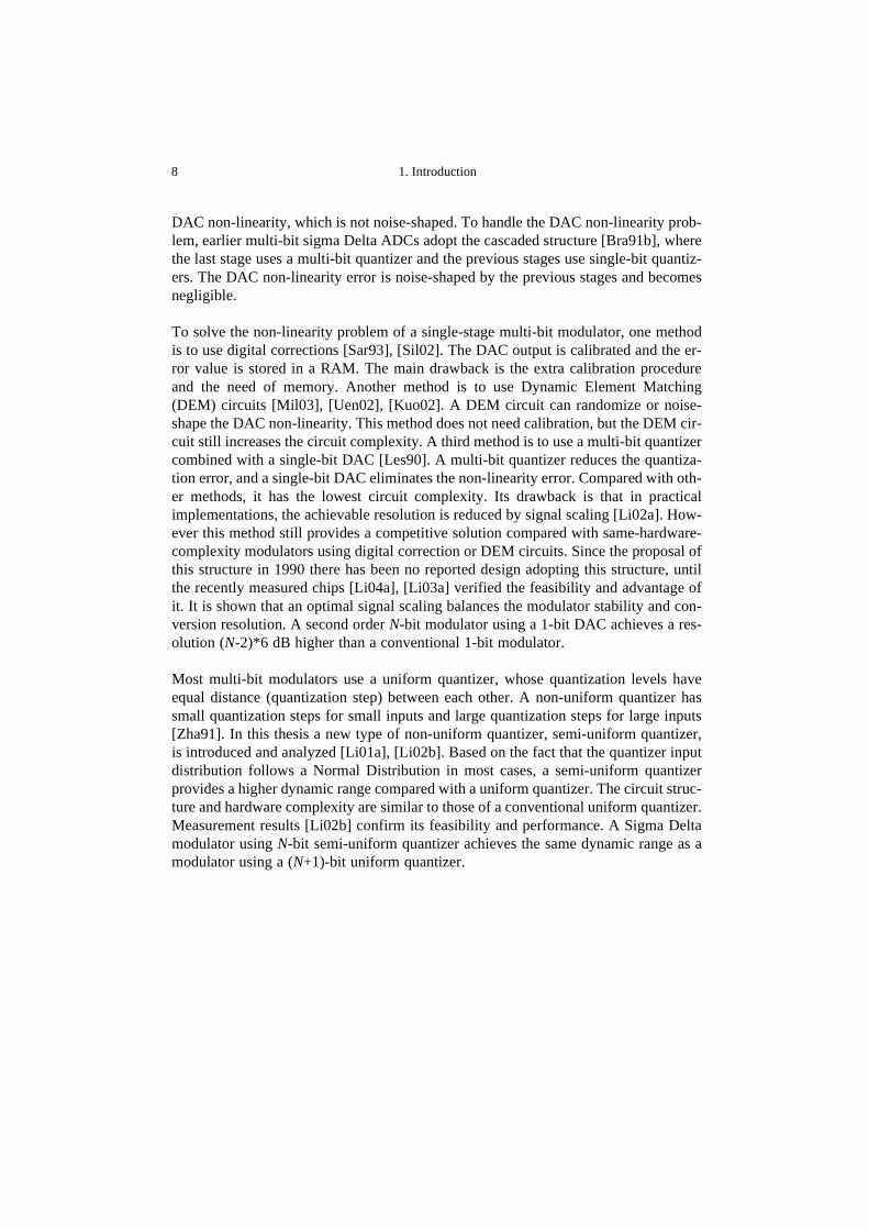
In a Sigma Delta A/D converter the quantization error is fed-back to the input of theconverter, thus the quantization error is shaped by the noise transfer function (NTF).The basic form of a NTF is:
Here k is the modulation order. Note that k=0 is the special case in which no noise-shap-ing is performed. The frequency response of such a NTF is
f
PSD
fb (=fs/2OSR) fs/2
1
2N 1–
12OSRfb
----------------------------------------
fi
f
PSD
fb (=fs/2OSR) fs/2fi
NTF z( ) 1 z1–
–( )k
= (2.5)
Sigma Delta ADC principle 13
Fig 2.6 plots the frequency response of NTF with different order k.
Fig 2.6 Noise transfer function
The in-band noise power is
So,
Compared with Equation 2.4, where the input signal is only oversampled withoutnoise shaping, the in-band quantization error power is much smaller. From this equa-tion we can also see that oversampling is the essential condition for a noise shaping
NTF f( ) 2 π ffs---
sink
= (2.6)
Pinband ρ2f( )NTF
2f( ) fd
0
fb
∫∆2
6fs------- 2 π f
fs---
sin2k
fd0
fb
∫= =
fs fb» π ffs---
sin π ffs---≈when we have
Pinband∆2
12------ π2k
2k 1+( )--------------------
2fb
fs-------
2k 1+≈ Pe
π2k
2k 1+--------------- 1
OSR2k 1+
------------------------= (2.7)
2. Sigma Delta ADC Overview14
modulator, because if OSR=1 (means no oversampling) then Pinband becomes
It is now possible to derive the maximum achievable SNR for an ideal Sigma Deltamodulator, which is used in Equation 1.4. For a normalized full-scale range of -1~+1input sinusoidal signal, the maximum signal power is
For a m-bit quantizer, the quantization step is
Therefore
Equation 2.9 shows that even with a coarse 1-bit quantizer, superior SNR can beachieved by combining a large oversampling ratio with a high noise shaping order.However, the real performance can be significantly lower than the equation predictiondue to three main reasons: 1. circuit non-idealities make the noise transfer function de-viate from its ideal form. 2. with stability considerations high order modulators are of-ten designed to have extra poles in their noise transfer functions, which increases thein-band noise power [Rit90]. For MASH structure modulators, the inter-stage signalscaling has the same effect of increasing in-band noise power. 3. circuit thermal noiseand flicker noise put a fundamental limit on the highest SNR that can be achieved, nomatter what the oversampling ratio or noise shaping order is.
2.1.3 Modulator topology
An integrator is a basic building block to construct a Sigma Delta modulator. Fig 2.7shows a first order Sigma Delta modulator.
Higher order modulators can be constructed in two ways. The first is to place integra-tors in a single loop, one following another. Feed-forward path can be added from sig-nal input to each integrator, and feed-back path can be added from DAC output to eachintegrator, as shown in Fig 2.8. Please note that each feed-forward or feed-back pathhas a coefficient associated with it, which is not shown in the figure for simplicity.
Fig 2.8 Single-loop modulator
The modulator in Fig 2.8 forms a noise transfer function NTF with all its zeros locatedat dc (z=1). It is possible to add some local resonator feedbacks as shown in Fig 2.9 tomove some of the NTF zeros away from dc, and as a result the in-band noise powercan be reduced.
Fig 2.9 Modulator with local feedback
The other way to construct a higher order modulator is to place the integrators in sev-eral loops [Hay86] as shown in Fig 2.10. This is the so-called MASH (multi-stagenoise-shaping) structure, or cascaded structure.
Fig 2.10 MASH structure modulator
inout
∫ ∫ ∫∫ ADC
DAC
inout
∫ ∫ ∫∫ ADC
DAC
Σ-∆ modulator
Σ-∆ modulator
Σ-∆ modulator
error canceling
in
out
2. Sigma Delta ADC Overview16
Each loop in Fig 2.10 forms an independent Sigma Delta modulator. The output ofeach modulator is sent to the error cancelling circuit. The overall noise-shaping orderis the sum of the noise-shaping orders of all stages.
2.1.4 Decimation filter
Decimation is a step to recover the narrow band signal from a high frequency datastream (very often a bit stream) generated by a Sigma Delta modulator [Sar88], [Sar90],[Kar92]. The decimation filter should provide enough attenuation to out-of-band noise,meaning that the design task of the low-pass filter is shifted from analog domain to dig-ital domain. However in digital domain designing such a filter is much easier. The char-acter of the filter depends solely on the digital coefficients rather than on the analogcomponent matching. A widely used design method for Sigma Delta modulator deci-mation filter is to combine a comb filter with a FIR filter [Cro81]. This method achievesboth circuit simplicity and linear phase response.
A comb filter reduces the digital data rate from OSR*fN down to about 2~8 times of fN,where fN is the Nyquist frequency. The word length is increased accordingly. The suc-cessive FIR filter further reduces the sampling frequency to fN. The reason why a combfilter is especially effective for Sigma Delta modulator is illustrated in Fig 2.11.
In Fig 2.11a the general specification of a decimation filter is shown. The sampling fre-quency should be reduced from fs to an intermediate frequency fD. To avoid aliasing,large attenuation is required outside the band 0 ~ fD/2. The transition band (fb ~ fD/2) isvery narrow compared to the sampling frequency fs. A large number of taps is neededif a FIR filter is used instead. However, the signal band between fb and fD/2 will be fil-tered-out by the successive FIR filter. This means the noise aliased into this range willnot increase the final in-band noise power, as long as the successive FIR filter providesenough stop band attenuation. As shown in Fig 2.11b the band ifD-fb ~ ifD+fb (i=1,2,...)should have enough attenuation because they will alias back to the signal band, whilethe other bands become "don’t care" region. This leads to the use of a comb filter whichhas a frequency response as shown in Fig 2.11c.
The comb filter has a z-domain transfer function of:
where d is the decimation factor and F is the filter order. The frequency response of acomb filter with order 1~3 is plotted in Fig 2.12.
H z( ) 1
dF
------ 1 zd–
–
1 z1–
–---------------- F
= (2.10)
Sigma Delta ADC principle 17
Fig 2.11 Anti-aliasing in comb filter(a) filter specification(b) don’t-care band(c) comb filter frequency response
fD fs/22fD 3fD 4fD
(b)
fb
fD fs/22fD 3fD 4fD
(a)
fb
stopband
stopband
stopband
stopband
don’t
band care
don’t
band care
don’t
band care
fD fs/22fD 3fD 4fD
(c)
fb
fD2
fD2
don’t
band care
2. Sigma Delta ADC Overview18
Fig 2.12 Comb filter response
It is proved [Can86] that for a modulator with an order k, a comb filter needs an orderat least k+1 to achieve enough stop band attenuation. The transfer function of quantiza-tion error for combined Sigma Delta modulator and comb filter is thus
and this will increase the equivalent in-band noise to
In an oversampling Sigma Delta converter normally , so the factoris very close to 1 and the in-band noise increase is negligible.
Following the comb filter one (or several) FIR filter is normally used. This FIR filterfurther reduces the sampling frequency to Nyquist frequency and truncates the outputword length to the specified value.
H z( ) 1
dk 1+
------------ 1 zd–
–( )k 1+
1 z1–
–( )------------------------------=
ρ′ f( ) ρ f( )c f fs⁄( )sin
c df( ) fs⁄( )sin---------------------------------=
df fs⁄ 1 4⁄≤c f fs⁄( )sin
c df( ) fs⁄( )sin---------------------------------
Quantizer characters 19
2.2 Quantizer characters
2.2.1 Quantizer transfer curve
A N-bit quantizer maps its input analog level to one of 2N digital codes. In the specialcase of 1-bit quantizer, there are only two output codes. The transfer curve representshow the quantizer maps the input level to a specific output code. Fig 2.13 shows a typ-ical example of a 3-bit quantizer transfer curve. The input values where the outputcode has a transition are thresholds of the quantizer. The output is digital levels, but ithas its analog equivalent. The analog equivalent of the distance between adjacent dig-ital codes is called quantization step ∆. The curve that crosses the midpoints of thequantization levels defines the gain of the quantizer. Most multi-bit quantizers have again of unit. For a single-bit quantizer, since there are only two output levels, the gaincan be arbitrary value.
Fig 2.13 Quantizer transfer curve
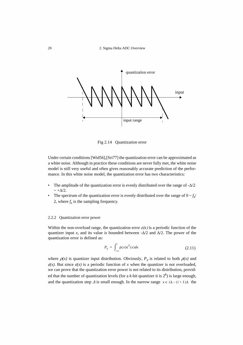
The quantization error is defined as the difference between the quantizer input and theanalog equivalent of the quantizer output. Fig 2.14 shows the quantization error corre-sponding to the transfer curve shown in Fig 2.13. When the quantizer is not overloadedthe quantization error is bounded within the range -∆/2 ~ +∆/2. The quantizer’s inputrange is defined as the range where the quantizer is not overloaded, that is -1-∆/2 ~1+∆/2 (normalized).
input
analog equivalentof digital output
input range
outputrange
∆
2. Sigma Delta ADC Overview20
Fig 2.14 Quantization error
Under certain conditions [Wid56],[Sri77] the quantization error can be approximated asa white noise. Although in practice these conditions are never fully met, the white noisemodel is still very useful and often gives reasonably accurate prediction of the perfor-mance. In this white noise model, the quantization error has two characteristics:
• The amplitude of the quantization error is evenly distributed over the range of -∆/2 ~ +∆/2.
• The spectrum of the quantization error is evenly distributed over the range of 0 ~ fs/2, where fs is the sampling frequency.
2.2.2 Quantization error power
Within the non-overload range, the quantization error ε(x) is a periodic function of thequantizer input x, and its value is bounded between -∆/2 and ∆/2. The power of thequantization error is defined as:
where ρ(x) is quantizer input distribution. Obviously, Pε is related to both ρ(x) andε(x). But since ε(x) is a periodic function of x when the quantizer is not overloaded,we can prove that the quantization error power is not related to its distribution, provid-
ed that the number of quantization levels (for a k-bit quantizer it is 2k) is large enough,
and the quantization step ∆ is small enough. In the narrow range the
input
input range
quantization error
Pε ρ x( )ε2x( ) xd
∞–
∞
∫= (2.11)
x i∆ i 1+( )∆∼∈
Quantizer characters 21
probability density ρ(x) can be approximated as a constant ρi, where
. This is shown in Fig 2.15.
Fig 2.15 Approximation of quantizer input distribution
Therefore we have:
This result concludes that the total quantization error power is only related to the valueof the quantization step ∆, and it is not signal dependent.
2.2.3 Quantizer gain
As mentioned in 2.2.1, a single-bit quantizer does not have a fixed gain. In its linearmodel the quantizer gain is determined by the loop coefficients based on the unit-loop-gain assumption. Fig 2.16 is an example of the linear model of a second order single-bit modulator. In the linear model, the 1-bit quantizer is modelled as a gain block αplus a white noise source e. Since the two-level quantizer can not define a fixed gain,α can take arbitrary value. But in practice, one often uses unit-loop-gain assumptionto assign a virtual linear gain to α. The unit-loop-gain assumption assumes that theproduct of integrator gain and the quantizer gain along the outer feedback loop is unit,or in Fig 2.16, b1a2α=1. This leads to α=1/b1a2. So the 1-bit quantizer linear gain isdefined by the modulator loop coefficients. This brings freedom to signal scaling pro-cedure, where the loop coefficients are adjusted to change the internal signal swingwhile the specified noise transfer function is kept constant. Since α can be set to any
i 2k 1–
– 2k 1–
1–,[ ]∈
ρ(x)
x
ρ0ρ-1 ρ1 ρ2ρ-2
∆
Pε ρ x( )ε2x( ) xd
∞–
∞
∫ ρ x i∆+( )ε2x i∆+( ) xd
0
∆
∫i 2k 1––=
2k 1– 1–
∑ ρ x i∆+( )ε2x( ) xd
0
∆
∫i 2k 1––=
2k 1– 1–
∑
ρi
i 2k 1––=
2k 1– 1–
∑ ∆
2--- x– 2
xd0
∆
∫⋅1∆--- ∆
2--- x– 2
xd0
∆
∫1∆--- ∆3
4------ ∆3
2------–
∆3
3------+
∆2
12------
= = =
= = = = (2.12)
2. Sigma Delta ADC Overview22
value, the product b1a2 can be adjusted to scale the internal signal swing.
Fig 2.16 Linear model of 1-bit modulator
In a multi-bit modulator, the quantizer gain is fixed, and in most cases it is unit. There-fore the value of α is 1. As a result, in signal scaling the product b1a2 is fixed toachieve the required noise transfer function. Accordingly, the linear model is muchmore accurate with a multi-bit quantizer. In general, the higher the quantizer bit-num-ber, the more accurate the linear model. In the extreme case where the quantizer hasinfinite number of bit, the model becomes perfectly linear.
2.2.4 Quantizer input distribution
For a Sigma Delta modulator, its input signal is unknown. Therefore the input distri-bution is also unknown. However the quantizer’s input distribution does have certaincommon characters, no matter what the modulator input is. Fig 2.17 shows the simu-lated quantizer input distribution of a second order modulator, with input signal set tosinusoidal, random, and dc respectively.
It is clear that all the distributions have a similar shape -- a Normal Distribution. Thefollowing analysis proves that when the modulator input signal amplitude is less thanhalf of quantizer LSB (Least Significant Bit) ∆, then its distribution does not signifi-cantly influence the distribution of the quantizer input, which is similar to a NormalDistribution.
In a Sigma Delta A/D converter the quantizer input is determined by both the inputsignal and the quantization error, due to the existence of the feedback loop. Generallyfor a kth order Sigma Delta modulator whose output in z-domain is
the quantizer input Q can be expressed as
X
z-11 a2a1
b1 b2
α
e
1-bit quantizer
z-11
Y
Y z( ) X z( )zk– ε z( ) 1 z
1––( )
k+=
Q z( ) X z( )zk– ε z( ) 1 z
1––( )
k1–[ ]+=
Quantizer characters 23
Fig 2.17 Quantizer input histogram
With a specific example of a 2nd order modulator,
Rewrite this equation in time domain,
Under the white noise assumption, the quantization error εn-1 and εn-2 are not correlat-
ed to input signal xn-2. Note that εn-1 and εn-2 are related to each other since ε(z)z-2 is
sinusoidal inputamplitude = 0.1
random inputamplitude = 0.1
dc input amplitude= 0.1
Q z( ) X z( )z2– ε z( ) 2z
1–– z
2–+( )+=
(2.13)Qn Xn 2– 2εn 1–– εn 2–+( )+=
2. Sigma Delta ADC Overview24
simply the one-sample-delayed version of ε(z)z-1. However at each specific sampletime the values of εn-1 and εn-2 are not correlated provided that the white noise modelholds. Therefore when we discuss the power and distribution of the quantizer input Qn,the variables xn-2, εn-1 and εn-2 can be treated as three independent variables.
Based on Equation 2.13, we have for uniform quantizer:
The power of quantizer input σ2q is the sum of input power σ2
x and five times of quan-
tization error power σ2ε. When σx is less than ∆/2, σq is mainly determined by quan-
tization error power. Fig 2.18 shows the simulated quantizer input power of a 2ndorder 3-bit Sigma Delta modulator, compared with the calculated value using Equation3.4. When the signal amplitude is less than ∆/2 the quantizer input power curve is al-most flat, which means the quantizer input power is dominated by the quantization er-ror power. When the signal amplitude exceeds ∆/2 the quantizer input power increasesrapidly and is dominated by the signal power.
Fig 2.18 Quantization error power
Not only the power but also the distribution of quantizer input Q is determined by boththe input signal and the quantization error. We will first focus on the quantization errorpart in equation 3.3. Since -2εn-1 (denoted as e1 later) and εn-2 (denoted as e2 later) aretreated as white noise, if we define y=e1+e2, the distribution ρy can be expressed as:
(2.14)σq2 σx
22
21
2+( )σε
2+ σx
25σε
2+ σx
2 512------∆2
+= = =
Quantizer characters 25
The detailed derivation of the above equation is presented in the attached paper 2.
Fig 2.19 shows the simulated quantizer input distribution of a 2nd order 3-bit modu-lator compared with the calculated curve using equation 2.15, when the input signalamplitude is negligible.
Fig 2.19 Quantizer input distribution
When the input signal is also taken into consideration the distribution of Q becomesmuch more complicated. It is not possible to give a close form of Q’s distribution be-cause the input signal x is an unknown waveform. But generally if the amplitude of xis relatively small compared with ∆/2, the distribution of Q will be similar to the onein Fig 2.19 but have a larger value at the center and a smaller value at the sides, giventhat x and ε are not correlated. Thus the distribution of Q would appear more similarto a Normal Distribution (Gaussian distribution), or in other words, Q is more likely
ρy k( )
0
32---∆ k+
2∆2( )---------------------
12∆-------
32---∆ k–
2∆2( )---------------------
=
when k 3∆( ) 2⁄>
3∆ 2⁄–( ) k ∆ 2⁄–( )≤ ≤when
∆ 2⁄–( ) k ∆ 2⁄( )≤ ≤when
∆ 2⁄( ) k 3∆ 2⁄( )≤ ≤when
(2.15)
2. Sigma Delta ADC Overview26
to have a small amplitude than a large amplitude. As will be discussed later, this is theessential condition to take the advantage of non-uniform quantization.
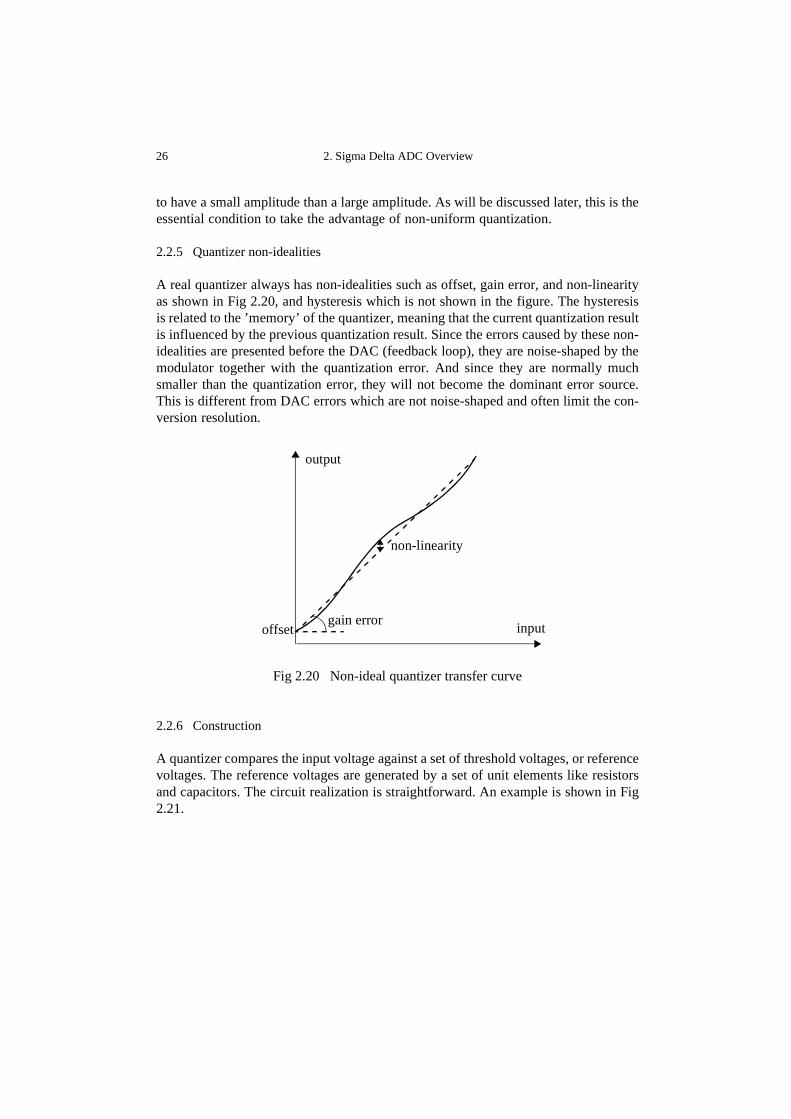
2.2.5 Quantizer non-idealities
A real quantizer always has non-idealities such as offset, gain error, and non-linearityas shown in Fig 2.20, and hysteresis which is not shown in the figure. The hysteresisis related to the ’memory’ of the quantizer, meaning that the current quantization resultis influenced by the previous quantization result. Since the errors caused by these non-idealities are presented before the DAC (feedback loop), they are noise-shaped by themodulator together with the quantization error. And since they are normally muchsmaller than the quantization error, they will not become the dominant error source.This is different from DAC errors which are not noise-shaped and often limit the con-version resolution.
Fig 2.20 Non-ideal quantizer transfer curve
2.2.6 Construction
A quantizer compares the input voltage against a set of threshold voltages, or referencevoltages. The reference voltages are generated by a set of unit elements like resistorsand capacitors. The circuit realization is straightforward. An example is shown in Fig2.21.
offset
non-linearity
gain errorinput
output
Quantizer characters 27
Fig 2.21 Quantizer realization
R/2
R/2
R
R
R
R
R
R
“1”
“1”
D7
D6
D5
D4
D3
D2
D1
D0
quantizer input
3 Multi-bit Modulators for Wireless communications
3.1 Wireless communication history
According to ITU’s (International Telecommunication Union) definition, Telecommu-nication is any transmission and/or emission and reception of signals representingsigns, writing, images and sounds or intelligence of any nature by wire, radio, opticalor other electromagnetic systems. When the media is radio, it is called wireless com-munication or radio communication. The history of wireless communication can betraced back to the nineteen’s century. The following list shows some of the importantmilestones in the early stage of wireless communication:
1820 Discovery of electromagnetism by Hans Christian Oersted and Andre-MarieAmpere.
1864 James Clerk Maxwell proved the existence of electromagnetic waves. 1887 Heinrich Hertz sent and received wireless waves.1895 Guglielmo Marconi sent morse radio signals. 1901 Marconi received the morse message sent across the Atlantic. 1907 Commercial Trans-Atlantic Wireless Service put into use. WWI Rapid development of communications intelligence, intercept technology,
cryptography. 1915 Wireless voice transmission from New York to San Fransisco. 1920 Marconi discovered short wave radio.1920 First commercial radio broadcast (in Pittsburgh) 1921 Police car dispatch radios, Detroit. 1930 BBC began television experiments. WWII Rapid development of radio technology.
3.1.1 Technology evolution
In the early phase, the transceivers were realized using vacuum tubes (an receiver ex-ample is shown in Fig 3.1) or later discrete semiconductor devices (an receiver exam-ple is shown in Fig 3.2). The large space and power consumption as well as the costmake it impossible to realize the idea of personal communication. With the inventionand fast development of integrated circuit (IC) technique, more and more signal pro-cessing (analog or digital) functions can be integrated into a single tiny chip. The mo-bile transceivers are made small enough to put into pocket, low-power enough to usebatteries, and cheap enough to be affordable by normal domestic users.
Wireless communication history 29
Fig 3.1 "All-american" 5-tube radio
Fig 3.2 Early pocket radio
3.1.2 Spectrum allocation
The hardware development is only one of the essential conditions for the realizationof personal communication. Another problem to be solved is the spectrum manage-ment. The radio spectrum available for public use is limited while the demand of it ishuge, considering that thousands of people need to talk through mobile phones at thesame moment. This problem is cleverly solved by the cellular technique, which was
3. Multi-bit Modulators for Wireless communications30
first developed and experimented in the Bell Laboratory. The basic idea is that a ser-vice area (e.g. a city) is spitted into many cells. In each cell there is a base station com-municating with mobile terminals. The power of the base station signal is so small thatthe signal will not spread much further out of that particular cell. As a result, the fre-quency band used in this cell can be re-used in other cells that are far away from it. Aconcept diagram of a cellular system is shown in Fig 3.3.
Fig 3.3 Concept of cellular technique
3.1.3 Three generations of cellular systems
In the short history of cellular systems, three generations have been developed.
1G (1st Generation) systems
Using the cellular technique, the 1G systems have higher capacity and greater mobilitysupport than earlier wireless radio networks. The 1G systems are analog systems,meaning that the signal is processed and transported in analog format. Examples of 1Gsystems are NAMTS in Japan, NMT-450 (later NMT-900) in Scandinavia, AMPS inUSA, C-450/NETZ-C in Germany, and TACS in UK.
2G systems/2.5G systems
The second generation (2G) wireless systems are characterized by the use of digitalradio transmission. Using hierarchical cell structures and multiple access technologieslike CDMA and/or TDMA, the system capacity is further extended compared with 1Gsystems. The largest 2G system currently in operation is the GSM family, includingthe original GSM 900MHz system, the higher frequency GSM 1800 MHz systemwhich is also called DCS1800 (Digital Communication System), and the US version
Wireless communication history 31
of DCS1800 - GSM 1900MHz, which is also called PCS1900 (Personal Communica-tion System). As shown in Fig 3.4, by February 2003 the GSM family holds 70 percentof the global cellular phone market. The second largest system is the IS-95 CDMA,which dominates the US market. Different from GSM, which uses time-division-mul-tiple-access technique, the IS-95 system uses code-division-multiple-access technique.Beside GSM, In US there are other TDMA systems, e.g. IS-54 (later IS-136). In Japanthe main system is PDC (Personal Digital Cellular).
Fig 3.4 World cellular phone subscribers
The 2.5G systems are updates of 2G systems with improved data communication ca-pability. In GSM system the data rate is only 9.6 kbps. The HSCSD (High Speed Cir-cuit Switched Data) system is an update of GSM by using several time slotssimultaneously when sending or receiving data from mobile users. The speed can beup to 57.6 kbps. Similar to GSM, HSCSD still uses circuit-switching technology totransfer data. In circuit switching, a communication channel is opened and dedicatedto a user for the duration of the communication. A more revolutionary development isthe GPRS (General Packet Radio Service) and EDGE (Enhanced Data rates for GlobalEvolution) systems, both using packet-switching technology. Packet switching splitsthe user’s data into small parts called packets. Packet switching uses the communica-tion system more effectively and enables users to be "always online" without the needof dial-up. The theoretical data rate is 144 kbps for GPRS and 384 kbps for EDGE.
3G systems
The data rates provided by 2G or 2.5G systems are not enough in cases like large im-age or video transfer. The 3G systems are developed to satisfy such requirements.There are three 3G standards under development: WCDMA proposed in Europe,
0
100
200
300
400
500
600
700
800
900
GSM CDMA US-TDMA PDC others
world cellular phone subscribers by Feb. 2003 (in million)source: EMC world cellular database
3. Multi-bit Modulators for Wireless communications32
CDMA2000 proposed in America, and TD-SCDMA proposed in China. They all useCDMA access technique and support up to 2Mbps data rate. The standards of 3G sys-tems are still under development and the commercial operation has just started.
3.2 Wireless receiver structure
3.2.1 Superheterodyne structure
Nearly all wireless receivers adopt the "superheterodyne" structure, where a radio fre-quency (RF) signal is frequency-translated to a much lower intermediate frequency(IF) signal using a mixer. A traditional superheterodyne digital receiver’s block dia-gram is shown in Fig 3.5.
Fig 3.5 Superheterodyne receiver
Since the IF signal frequency is fixed, the gain stage and IF filter are easy to design.The requirement on the ADC is low because the neighboring channels are filtered out.Due to its superior performance, the superheterodyne structure is the dominant choicein transceiver design. However the main drawback of the conventional superhetero-dyne structure is the low integration level. The RF filter, IR filter and IF filter are noteasy to be integrated into transceiver front-end chips with a reasonable performance incurrent technology level. It is the need of low cost, small size, and low power thatstimulates the development of new transceiver structures with reduced number and/orrequirement on filters. In a traditional superheterodyne transceiver the channel selec-tion is done in analog domain by IF filters. To largely attenuate the out-of-band signalor noise, the IF filter needs a sharp edge, making it difficult to be integrated. On theother hand, since the input to the ADC is already channel-selected, only the wantedsignal is there and the requirement on the ADC is low. If not only the wanted signalbut also the neighboring channel is sent to the ADC and converted to digital signal,then the channel selection is performed in digital domain. In digital domain it is mucheasier to make the channel selection programmable, and the cost is lower. The draw-back is that the wanted signal must be converted together with the much larger neigh-boring channel or blocker signal, putting a very strict dynamic requirement (normallyabove 12bit) on the ADC. The ultimate target of the so-called "software radio" is toeliminate all the analog components in a receiver except the RF filer and the LNA. The
LNA ADC
RF IR IF
LO1 LO2
Wireless receiver structure 33
filtered RF signal is directly converted by a super-ADC. The converted signal is thendigitally channel-selected and processed. The bandwidth and resolution requirementon the ADC in such a software radio is so high that it is impossible to realize in thenear future. Even if it becomes technically feasible to design such an ADC in the fu-ture, it would take longer time to make it economically feasible. The currently feasibleand often used high-integration structures are low-IF and direct conversion structures.
3.2.2 Direct conversion (homodyne) structure
The direct conversion structure is also called zero-IF structure, or homodyne structure.The RF signal is directly mixed to base-band. The IF stage is cancelled and the signalis the image of itself. It is much simpler compared with traditional superheterodyne re-ceivers as shown in Fig 3.6, and the required external components are largely reduced.The main drawbacks are 1) the mixer output might contain large dc offset caused byself-mixing of the leakage oscillator signal with the oscillator signal itself, and 2) theflicker noise (1/f noise) of the mixer can not be filtered since the mixer output is cen-tered at dc. Therefore although it has a relatively long history, this structure is notwidely used until recently. Nowadays many mobile receivers (e.g. from Alcatel, Eric-sson, Nokia) adopt the homodyne structure.
Fig 3.6 Homodyne receiver
3.2.3 Low-IF structure
The low-IF structure is somewhere between the traditional superheterodyne structureand the homodyne structure, as shown in Fig 3.7. It has a much lower-than-normal IFfrequency, and thus avoids the main drawbacks of homodyne at dc. The whole IF bandcan be directly converted by a ADC, which can be either low-pass or band-pass. Likea homodyne, a low-IF receiver needs fewer external components and is easier to beintegrated compared with the traditional superheterodyne structure. The drawback isthat the image signal cancelling has to be performed by an image-rejection mixer,whose performance varies with process variations and temperature changes.
Fig 3.7 Low-IF receiver
LNA ADC
RF
LO
LNA ADC
RF
LO
3. Multi-bit Modulators for Wireless communications34
3.3 Sigma Delta ADC in receivers
Table-1 lists some of the recently reported Sigma Delta ADCs or modulators designedfor wireless transceivers/receivers. Their characteristics are summarized in the table.
When designing receivers for 2G systems, like GSM or CDMA, the signal bandwidthis within several hundred KHz. In that kind of bandwidth range, 12~16 bit resolutioncan be well achieved with current design and process technology. When migrating to3G systems, the signal bandwidth goes into MHz range. The achievable resolution isreduced. As described before, in a receiver the higher resolution and bandwidth anADC can achieve, the lower requirement it is for the RF front-end. Therefore to im-plement a high-integration-level 3G receiver, further increase in resolution is neededfor current Sigma Delta ADCs, and at the same time the power consumption of ADCsmust be kept reasonably low. A multi-bit Sigma Delta ADC is a promising candidatefor these applications.
Table 1:
Ref RF stand. RFstruc.
proc-cess µm
ADC struc.
order BWKHz
DRdB
SNDRdB
power mW
FOM
x1010
[Dez03] WCDMAGPRS
zero-IF 0.13 SC3-bit
3 1920100
7082
6481
4.32.4
116
[Vel03] EDGE, CDMA2000 ,UMTS
low-IF/ zero-IF
0.18 CT1-bit
5 200,1228,3840
92,83,74
92,83,74
3.8,4.1,4.5
699
[phi03] bluetooth low-IF 0.18 CT 1-bit
5 1000 76 75.5 4.4 221
[mil03] CDMA 0.18 SC6-bit
2 615 77 30 26
[Vel02] UMTS zero-IF 0.18 CT1.5-bit
4 2000 70 68 3.3 249
[Gom02] GSM,UMTS
0.13 SC5-level
2 200,2000
79,50
75,49
2.4,2.9
76.6
[Bur01] GSM,UMTS
superhet-erodyne
0.25 SC1-bit
2 200,3840
86,54
72,52
11.5,13.5
18.5
[Oli01] GSM,EDGE
low-IF 0.35BiC-MOS
SC1-bit
2-2 189 84 84 5 74.1
[Sal01] GSM,UMTS
superhet-erodyne
0.35 SC1-bit
2 270,3840
80,?
70,43.3
61.2 2.2
Non-uniform quantization 35
3.4 Non-uniform quantization
Most of quantization performed in A/D conversion is uniform quantization, whichmeans the quantization steps are equal. This is natural because the numbering systemwe use are uniform systems where the distances between adjacent numbers are thesame. The quantizer characters that are discussed in the previous section are all basedon uniform quantizers.
Although uniform quantizer is almost the exclusive choice in Sigma Delta ADCs, pos-sible applications of non-uniform quantizers were explored [Zha91]. Non-uniformquantizers have different quantization steps for inputs with different amplitudes. Totake the advantage of non-uniform quantization in Sigma Delta ADCs, the quantiza-tion steps should be arranged in such a way that small-amplitude input is quantized bysmall quantization steps and large-amplitude inputs by large steps.
3.4.1 Precondition to use non-uniform quantizer
The reason to use non-uniform quantizer is to reduce the overall quantization errorpower, which is expressed in equation 2.11 and repeated here:
As proved in section 2.2.2, for a uniform quantizer this power is a constant. Howeverfor a non-uniform quantizer this conclusion does not hold. For a non-uniform quantiz-er, its quantization error ε(x) is smaller than that of a uniform quantizer when the am-plitude of x is small, and its ε(x) is larger than that of a uniform quantizer when theamplitude of x is large. Therefore the precondition to use a non-uniform quantizer isthat the quantizer input distribution concentrates in the small-amplitude range, so thatthe overall noise power can be reduced by using a non-uniform quantizer. Fortunatelythis precondition is satisfied in a Sigma Delta modulator. In section 2.2.4 it is provedthat when the modulator input signal amplitude is small the quantizer input distribu-tion always has a form similar to a Normal Distribution, which means the quantizerinput is more likely to have a small amplitude rather than a large amplitude.
3.4.2 µ-law quantizer
[Zha91] proposed to arrange the quantization steps corresponding to µ-law. Such aquantizer has an exponential input-output transfer curve, and its corresponding DAChas a logarithmic input-output transfer curve. It is especially suitable for applicationslike voice processing. But to generate the threshold voltages for such a quantizer is noteasy. First, the largest quantization step could be tens of times larger than the smalleststep. Matching the quantization steps in such a wide range is difficult. Second, the dif-ferent quantization steps are not linearly changing, therefore it is not possible to useunit element to match these steps.
Pε ρ x( )ε2x( ) xd
∞–
∞
∫=
3. Multi-bit Modulators for Wireless communications36
3.4.3 semi-uniform quantizer
The name "semi-uniform" means that there are only two different-size quantizationsteps [Li01a] [Li03b], making it very similar to a conventional uniform quantizer. Thesmall quantization step is for small inputs and the large step for large inputs. Specifi-cally, for a k-bit semi-uniform quantizer with normalized full-scale range of -1 ~ +1,
the center 2k+1 quantization steps have a step size of , and the outer 2k-
1 quantization steps have a step size of ∆2=3∆1.
Fig 3.8 Semi-uniform quantization(a) transfer curve (b) quantization error
Fig 3.8a and Fig 3.8b show the quantization levels and quantization error of a 3-bit semi-uniform quantizer, compared with that of a 4-bit uniform quantizer. It can be seen that actu-ally the 3-bit semi-uniform quantizer’s 8 quantization levels are all "borrowed" from the 4-bit uniform quantizer’s 16 levels. As a result, the quantization error of the semi-uniformquantizer is also closely related to that of a uniform quantizer. At the four center steps thequantization error of both the 3-bit semi-uniform and 4-bit uniform quantizers are thesame, while at the outer steps the semi-uniform quantization error can be three times as
∆12
2k 1+
1–---------------------=
(a)
(b)
Non-uniform quantization 37
large as that of the 4-bit uniform quantizer. This implies that if most of the quantizer inputsfall into those small quantization steps, a k-bit semi-uniform quantizer could achieve thesame dynamic range as a (k+1)-bit uniform quantizer, as will be demonstrated shortly.
When using a semi-uniform quantizer, the quantization error ε is a function of the quantizerinput x. When x falls into those smaller quantization steps,
Here mod(a,b) is the modulo function with b as modulo. When x falls into those largerquantization steps and quantizer is not overloaded,
Here sign(a) is the sign function. When the quantizer is overloaded,
3.4.4 Semi-uniform quantizer/DAC design
One of the advantages of semi-uniform quantizer is its simple structure. The circuit of asemi-uniform quantizer can be constructed in the same way as a uniform quantizer. Theyuse the same number of comparators. The only difference is how the thresholds for thecomparators are generated. When using unit elements (e.g. resistor) to generate the thresh-old voltages, a semi-uniform quantizer needs double number of unit elements comparedwith a same resolution uniform quantizer. Since there are only two quantization steps, andthe bigger one is three times as large as the smaller one, matching is easy to realize. Fig 3.9shows a 3-bit uniform/semi-uniform dual-mode quantizer. In both modes the same set ofcomparators is used. The different threshold voltages are generated by two resistor ladders.The number and value of unit elements in two ladders are different. One of the two sets ofthreshold voltages is selected by a switch and fed to the comparator array.
Similarly, a 3-bit uniform/semi-uniform dual-mode DAC can be constructed, as shownin Fig 3.10. Two resistor ladders generate two sets of output analog voltages accordingto the input digital code. Through a switch, the selected one is sent to DAC output.
ε x( ) 1
2k 1+
1–--------------------- mod x
2
2k 1+
1–---------------------,–=
ε x( ) 3
2k 1+
1–--------------------- mod sign x( ) x
2k 1–
2+
2k 1+
1–---------------------–
6
2k 1+
1–---------------------,–=
ε k( ) sign x( ) 1 x–( )=
3. Multi-bit Modulators for Wireless communications38
Fig 3.9 Dual-mode quantizer
Fig 3.10 Dual-mode DAC
3.4.5 Measured performance
The advantage of semi-uniform quantizer is verified by a second order modulatorusing the demonstrated 3-bit dual-mode quantizer and DAC. At a 3V supply voltage thepower consumption is 9.3mW. Simulation results show that about 32% of the power is con-
sumed by the 3-bit quantizer and 41% by the two OTAs. The active chip area is 0.23mm2.At 6.4MHz sampling frequency and 32x oversampling ratio, the signal bandwidth is100kHz. Using a semi-uniform quantizer achieves a peak SNDR of 63.8dB and a dynamicrange of 81dB. Using a uniform quantizer achieves a peak SNDR of 54.1dB and a dynamic
Semi R-ladder Uni R-ladder
thresholds
uni/semiswitch
comparatorvin+ vin-
digital output
array
R ladder 1R ladder 2
Semi R-ladder Uni R-ladder
thresholds
uni/semiswitch
digi
tal c
ode
vout+ vout-
R la
dder
1
R la
dder
2
Non-uniform quantization 39
range of 70dB. Fig 3.11 shows the measured SNDR versus input amplitude. Comparing thespectrum of the modulator outputs with both quantizers in Fig 3.12, it can be seen that thenoise floor is significantly lower when using the semi-uniform quantizer.
Fig 3.11 SNDR comparison
Fig 3.12 Noise floor comparison
3. Multi-bit Modulators for Wireless communications40
3.5 Multi-bit modulator with 1-bit DAC
The biggest problem associated with a multi-bit Sigma Delta modulator is the multi-bit DAC nonlinearity problem. Since the DAC is located in the feedback loop, the er-ror caused by its non-idealities e.g. gain error, offset, and non-linearity will not benoise-shaped, which is the case for quantizer non-idealities. But the influence of theseDAC non-idealities are not the same. An offset causes a dc error at the modulator out-put, which is of no importance in most cases. A gain error adds extra poles to the noisetransfer function, and hence changes the in-band quantization error power slightly. Itsinfluence is often negligible. A non-linearity, however, is signal correlated. For eachspecific digital code, the DAC has a specific non-linearity error. This one-to-one de-terminacy between the non-linearity error and DAC input code causes distortion, in-stead of noise, in the modulator output as shown in Fig 3.13.
Fig 3.13 Second order 3-bit modulator output spectrum with 0.1% DAC non-linear error and -6dB input
Dynamic Element Matching (DEM) is the most popularly used circuit technique toreduce the influence of DAC non-linearity. The basic idea is to break the one-to-onedeterminacy between the non-linearity error and DAC input code, and thus break itssignal-dependence. As a result, the non-linearity will no longer cause in-band distor-tion. Instead it will cause either an increased noise floor or out-of-band distortions.Basic DEM algorithms include randomization [Car88], individual level averaging [Leu92],and data weighted averaging [Bai95].
3.5.1 DEM algorithms
The randomization algorithm randomly chooses a set of DAC elements at each clock cycleso that the DAC non-linearity error is turned into a white noise, whose power is mainly
frequency (Hz)
ampl
itude
(dB
)
caused by DAC non-linearity
Multi-bit modulator with 1-bit DAC 41
out-of-band and will be digitally filtered. Compare its spectrum in Fig 3.14 with Fig 3.13,it can be observed that the distortions disappear but the noise floor is increased slightly.
Fig 3.14 Second order 3-bit modulator output spectrum with randomization DEM
The individual level averaging algorithm sets a pointer for each DAC input digital code tomake sure that all the DAC elements are equally used for each digital input code. The DACnon-linearity error is partly noise-shaped, so its noise floor shown in Fig 3.15 is lower thanthat using randomization algorithm.
Fig 3.15 Second order 3-bit modulator output spectrum with individual level averaging DEM
The data weighted averaging algorithm sets one pointer to record the position of the DACelement that was last used, and each DAC element is guaranteed to be used equally often.The DAC non-linearity error goes through a first-order noise shaping, therefore its noisefloor as shown in Fig 3.16 is the lowest.
frequency (Hz)
ampl
itude
(dB
)
frequency (Hz)
ampl
itude
(dB
)
3. Multi-bit Modulators for Wireless communications42
Fig 3.16 Second order 3-bit modulator output spectrum with data weighted average DEM
3.5.2 Derivation
One way to solve the DAC non-linearity problem on circuit level is to use a 1-bit DACin a multi-bit Sigma Delta modulator [Les90]. The derivation of such a structure canbe illustrated in two ways.
Fig 3.17 Derivation from single-stage multi-bit modulator
The left side of Fig 3.17 is a conventional N-bit single-stage Sigma Delta modulator.In the feedback a N-bit DAC is used. If the data length is truncated from N-bit to 1-bit, a 1-bit DAC can now be used. The truncation error needs to be compensated dig-itally in the error-cancelling block.
frequency (Hz)
ampl
itude
(dB
)
loopfilter
N-bitquantizer
N-bitDAC
X Yloopfilterloopfilter
N-bitquantizerN-bitquantizer
N-bitDACN-bitDAC
X Yloopfilter
N-bitquantizer
1-bitDAC
X Y1
N-to-1 bittruncation
N-to-1 bittruncation
erro
rca
ncel
ing
Y
N1
loopfilterloopfilter
N-bitquantizerN-bitquantizer
1-bitDAC
X Y1
N-to-1 bittruncation
N-to-1 bittruncation
erro
rca
ncel
ing
Y
N1
Multi-bit modulator with 1-bit DAC 43
Fig 3.18 Derivation from MASH structure
Another way to understand the function of this structure is to start from a MASH struc-ture modulator, as shown in Fig 3.18. The orders of the two stages are M1 and M2,which is noted as M1-M2 MASH. The first stage uses a 1-bit quantizer, while the sec-ond stage uses a N-bit quantizer. The outputs from the two quantizers are combined inthe error-cancelling block to generate the modulator output. If the order of the secondstage is reduced to 0, then we get a M1-0 MASH structure. As a result, the loop filterand N-bit DAC in the second stage are skipped, only the N-bit quantizer remains.Since now the two quantizers have exactly the same input, the 1-bit quantizer can bephysically skipped because the output of the 1-bit quantizer is always equal to theMSB (Most Significant Bit) of the N-bit quantizer. Now it becomes a single-stagemodulator with a N-bit quantizer and a 1-bit DAC.
3.5.3 Linear model before signal scaling
In his original paper [Les90], Leslie provided a linear model analysis of the modulatorusing multi-bit quantizer and 1-bit DAC. The conclusion is that ideally this structurewill achieve exactly the same resolution as a conventional multi-bit modulator. In thatlinear model the quantizer is assumed to have a unit gain. For a conventional multi-bitmodulator this assumption is always true. For a 1-bit modulator the quantizer lineargain is defined by the loop coefficients. Assuming a unit quantizer gain means that nosignal scaling is performed to the modulator. Such a modulator can not be implement-ed and used, because the required internal signal swing is too large. After signal scal-ing, a 1-bit quantizer always has a linear gain larger than unit. A modulator combinga multi-bit quantizer and 1-bit DAC is basically a 1-bit modulator plus an extra multi-
loopfilter
N-bitquantizer
N-bitDAC
y2
digi
tal
corr
ectio
n
loopfilter
1-bitquantizer
1-bitDAC
X y1
N-bitquantizer
y2
digi
tal
corr
ectio
n
loopfilter
1-bitquantizer
1-bitDAC
X y1
YY
digi
tal
corr
ectio
n
loopfilter
N-bitquantizer
1-bitDAC
X Y
M1-M2 MASH
M1-0 MASH
Single-stage
loopfilterloopfilter
N-bitquantizerN-bitquantizer
N-bitDACN-bitDAC
y2
digi
tal
corr
ectio
n
loopfilterloopfilter
1-bitquantizer1-bitquantizer
1-bitDAC1-bitDAC
X y1
N-bitquantizerN-bitquantizer
y2
digi
tal
corr
ectio
n
loopfilterloopfilter
1-bitquantizer1-bitquantizer
1-bitDAC1-bitDAC
X y1
YY
digi
tal
corr
ectio
n
loopfilterloopfilter
N-bitquantizerN-bitquantizer
1-bitDAC1-bitDAC
X Y
M1-M2 MASH
M1-0 MASH
Single-stage
erro
rca
ncel
ing
erro
rca
ncel
ing
erro
rca
ncel
ing
3. Multi-bit Modulators for Wireless communications44
bit quantizer, as can be seen from Fig 3.18. Therefore the unit-quantizer-gain assump-tion does not hold for the modulator combining multi-bit quantizer and 1-bit DAC. Forexample, the linear model of such a second-order modulator before signal scaling andits integrator output histogram is shown in Fig 3.19. The reference voltage is normal-ized to +/-1. It can be observed that the quantizer is severely overloaded.
Fig 3.19 Linear model before signal scaling
3.5.4 Linear model after signal scaling
Fig 3.20 Linear model after signal scaling
In the linear model shown in Fig 3.20 the coefficients a1, a2, b1 and b2 are used to ad-just the internal signal swing. Here the N-bit quantizer is modelled as two separateones: a N-bit quantizer and a 1-bit quantizer. The output of the 1-bit quantizer is usedto drive the feedback. This makes the model easier to analyze, and makes it clear thatit is basically a 1-bit modulator plus a N-bit quantizer. Therefore the signal scaling pro-cedure is similar to that of a 1-bit modulator instead of a multi-bit modulator. For theN-bit quantizer, its gain is unit. For the 1-bit quantizer, its gain α is determined by the
X
z-11
z-11
2z-1-z-2
(1-z-1)2
Y2
N
1
N
int1
int2
X
z-11
z-11a2
b1
α
e1
α(1-z-1)2
2z-1-z-2
e2
N-bit
1-bit
Y
quantizerb2
a11
N
int1
int2
Multi-bit modulator with 1-bit DAC 45
coefficient b1 and a2: α=1/(b1a2). To reduce the internal signal swing b1 and a2 haveto be small enough. A common choice is to set a1=a2=b1=b2=0.5. The two integratoroutput histograms show that most quantizer inputs are bounded between +/- referencevoltages. But since the 1-bit quantizer gain α is set to be larger than unit, the N-bitquantization error is enlarged by a factor of α in the final modulator output:
A design consideration here is to optimize the value of α so that the quantization erroris not enlarged too much, while at the same time the internal signal swing is kept lowto ensure modulator stability [Rit90]. Generally, when the modulator order increases(in a single stage) the loop coefficients have to be scaled smaller to control the internalsignal swing, which leads to a larger α and therefore larger in-band quantization errorpower. For the second order modulator shown in Fig 3.20 the α is 4, introducing a12dB resolution reduction. For higher order single-stage modulators optimized usingthe MATLAB toolbox provided by Richard Schreier [Sch88], a third, forth, and fifthorder modulator has a quantizer gain of 23, 164, and 1428 respectively. It is obviousthat the resolution reduction is not affordable for a modulator order higher than 3. Thisimplies that a low order modulator can take more advantage by combing a multi-bitquantizer with a 1-bit DAC. In fact a first order Sigma Delta modulator is most suit-able for such a structure because it does not need to do signal scaling and thus its quan-tizer gain is unit. Unfortunately a first order modulator suffers from the problems oftones as well as high in-band quantization power, thus it is seldom used in practice.
3.5.5 Measured performance
The simulated performance of a second order modulator using 1~6 bit quantizers and1-bit DAC is plotted in Fig 3.21. The sampling frequency is 32MHz and the oversam-pling ratio is 16, corresponding to a signal band of 1MHz. The input sinusoidal signalis at 30kHz. Also plotted in the figure are measured results of such a modulator using5-bit quantizer and 1-bit DAC [Li03a]. Fig 3.22 compares the measured noise floorsof the output spectrum using a 5-bit quantizer and a 1-bit quantizer respectively. Whenusing a 5-bit quantizer the quantization error is much smaller than that of a 1-bit quan-tizer, as a result the noise floor is pushed down.
Y Xz2– α 1 z
1––( )
2e2+ Xz
2– 1 z1–
–( )2e2
b1a2-----------------------------+= =
3. Multi-bit Modulators for Wireless communications46
Fig 3.21 Measured 2nd order modulator SNDR
Fig 3.22 Measured 2nd order modulator spectrum
4 Future Design Challenges
4.1 Ultra low voltage design
4.1.1 Background
In the past decades the development of CMOS technology closely follows Moore’slaw. Most experts expect that this trend will continue at least in the near future. Oneaspect of the technology advance is the continuous decrease of gate oxide thickness.In order to prevent the electric field strength from being too high, the supply voltageshould be reduced in a similar scale. According to the ITRS (International TechnologyRoadmap for Semiconductors) roadmap 2001, the predicted gate oxide thickness, pro-cess feature size, and supply voltage are shown in Fig 4.1.
Fig 4.1 ITRS roadmap prediction
In 10 years from now the supply voltage for CMOS circuits will drop to 0.5V, mean-ing that many widely used analog circuit topologies will no longer be applicable.
4.1.2 Design problems in Sigma Delta modulator
Using switched-capacitor circuit is the most robust way to construct a high resolutionSigma Delta modulator. To make it work, the charge stored in capacitors must betransferred through switches. In a switched-capacitor circuit the switches can be divid-ed into two types, as shown in Fig 4.2 with the example of an integrator. Switches s2,s3 have one of their terminals connected to GND. Therefore as long as Vg > VGND+Vt,
4. Future Design Challenges48
the switch will conduct. Switch s4 has one of its terminals connected to the virtualground of the Opamp, therefore it can also be treated as connecting to the GND. Forthis type of switch a single NMOS transistor can be used. Switch s1 and s5 howeverhave both of their terminals ’floating’, not connected to a fixed voltage level. Since thesignal level can be any value between the power rails, a complementary switch has tobe used. The transconductance of such a complementary switch is shown in Fig 4.3.When Vdd>Vt,n+Vt,p, there is a signal range in which both the NMOS and PMOS tran-sistor conducts. When Vdd=Vt,n+Vt,p there is only one transistor conducting at anytime. In the case Vdd<Vt,n+Vt,p, there is a signal range in which none of the transistorsconducts, meaning the switch fails to work. Therefore the supply voltage must be larg-er than the sum of PMOS and NMOS threshold voltages to keep the complementaryswitch function properly. At an ultra low supply voltage, this condition is difficult tomeet. The design of OTA and comparator also becomes more difficult under a ultralow supply voltage.
Fig 4.2 Switched-Capacitor Integrator
Fig 4.3 Complementary switch transconductance a) Vdd>Vt,n+Vt,p b) Vdd<Vt,n+Vt,p
s1
s3
s4Ci
Ci
vout
vi s5next stageφ1 φ2 s2 φ1
φ2
φ1
vin
gs
NMOS conductPMOS conduct
both conduct
vin
gs
NMOS conduct PMOS conduct
none conduct
00
(a) (b)
Ultra low voltage design 49
4.1.3 Voltage multiplier
Using a voltage multiplier [Cas01] or boothstrapping [Des01] circuit to provide a highgate voltage for switches is currently often adopted. Only a small part of the circuitworks under a high voltage and the rest part of the circuit sees a normal supply volt-age. The drawback of this solution is obvious: 1. it is not a true low voltage design.The high gate voltage might break down the gate oxide layer, causing reliability prob-lem. 2) the voltage multiplier or boothstrapping circuit requires a large chip area andpower. So this solution is not a robust one when the process is further scaled down.
4.1.4 Switched opamp
One solution to the switch conducting problem is to replace the switch of S5 in Fig 4.2by a sample-hold buffer [Cro94], [Pel97]. The buffer samples the previous Opampoutput at one clock phase, and buffer it to the next stage at another clock phase. Thecircuit is shown in Fig 4.4. Since now all the switches have one of its terminals con-nected to GND, they are able to conduct as long as Vdd>Vt,n. The price for the solutionis that the Opamp has to be switched on and off every clock cycle, because its outputwill be shortened to GND in one of the phases. This causes the drawback of low speed.Currently the switched-opamp circuit speed is around 10MHz. [Che02].
Fig 4.4 Switched-opamp circuit
4.1.5 Low/Zero Vt process
Since the supply voltage Vdd must be larger than Vt,n+Vt,p to make the switch functioncorrectly, the most straightforward solution is to use low-Vt or even zero-Vt process[Ada90], [Baz95a]. This kind of process also eases the design of Opamp and compar-ator. Nowadays many circuits are designed with multi-Vt process, where low-Vt MOStransistors can be used when needed. The cost of such processes are higher than stan-dard CMOS processes. But with the continuous advance of processing technology, theincrease need for such multi-Vt processes will make it become a commonly used stan-
sb
scCs
voutφ2 sa φ1
φ2
Ci
Ci
sd φ1se φ2
4. Future Design Challenges50
dard. Once widely adopted, the process cost will be reduced dramatically. Anotherconcern about the low/zero Vt process is the leakage current. The subthreshold currentof a MOS transistor is:
The coefficient Ist and parameters σ and n are determined empirically. It can be ob-served that 1) the subthreshold current drops exponentially with VGS, and 2) the sub-threshold current is closely related to the value of Vt. When Vt is reduced, leakagecurrent increases dramatically. For a switched-capacitor integrator a leakage currentcauses a charge-leakage, which in turn causes an output voltage change.
The subthreshold current can be well controlled within the order of pA, by using seriestransmission gate [Baz95b] or increasing the source to substrate voltage [Baz95a]. Asa rule of thumb, a 100dB SNR switched-capacitor circuit with a power supply of 1Vand an switch-on-resistance of 10kOhm requires a subthreshold current less than 1nA[Baz95b]. Therefore the leakage current will not become the performance bottleneckwhen using low/zero-Vt process.
4.2 Substrate coupling
With the development of design and process technique, a Sigma Delta ADC can bemade smaller and less power consuming. Hence it is easier to embed a Sigma DeltaADC into a complex mixed-signal chip. The noise coupled from digital part will in-fluence the function of sensitive analog circuit, e.g. a ADC.
4.2.1 Coupling noise source
The noise can couple from digital part to analog part through substrate in two mannersas shown in Fig 4.5. The first way is that digital block switching noise can be injectedinto substrate and then coupled into the analog circuit. The second way is that digitalcircuit switching current causes di/dt noise on the digital power rails. Although thedigital part and analog part may have physically separated power rails, the di/dt noisecan still couple to the analog power rails through the common substrate. And once thepower rails are contaminated with noise, the whole analog circuit will be influenced.Therefore the latter coupling path is often the most critical coupling path.
IDS Iste
VGS σVDS Vt–+
nkt q⁄----------------------------------------
=
Substrate coupling 51
Fig 4.5 Coupling noise path
4.2.2 Substrate model
The substrate coupling is strongly influenced by the layout floorplan, substrate materialcharacteristic and biasing voltages.
Two types of wafer are usually used in semiconductor process: lightly-doped wafer andheavily-doped wafer. The latter kind of wafer is good for avoiding latch-up. The explo-ration of substrate characteristic can be carried out using device-level simulator likeMEDICI. However its capability is limited to small circuits and it takes very long timeto do a simulation. In order to find the coupling noise influence on a circuit, the sub-strate model should be integrated into SPICE-like circuit-level models. Starting fromPoisson’s equation [Ver93] or from simplified Maxwell’s equation [Ver96], the follow-ing description of the substrate can be derived:
where E is the electric field intensity vector, ρ and ε are the sheet resistivity and dielec-tric constant of the semiconductor respectively. It is impossible to give a closed-formanalytical solution of this substrate description in practice. A practical way is to decom-pose the whole substrate into a 3-D mesh and use numerical calculation to find a rea-sonably accurate solution. An element of such a mesh is shown in Fig 4.6:
analog part digital part
VddD
VssD
substrate
VddA
VssA
εt∂
∂ ∇E( ) 1ρ---∇E+ 0=
4. Future Design Challenges52
Fig 4.6 Mesh element of substrate model
Each substrate element has six resistor-capacitor pairs connecting to its six neighboringelements. When the system operation speed is under the order of GHz, the capacitors inthe model can be neglected without causing much degradation to the modeling accura-cy. The equation describing the relation between node i and one of its neighbor j is
The density of the mesh network directly determines the substrate modelling accuracy.In practice the available computation capability limits the mesh node number. In[Cle94] a non-uniform density mesh structure is proposed so that the sensitive areawould have a higher density. But even this method could only handle relatively smallcircuits. In particular, consider the case of Sigma Delta converter, thousands of clockcycles need to be simulated to do an accurate FFT analysis. This limits the substratenode number to be in the same order of circuit device number. To solve this problem, amacro model has to be used, where the substrate macro model is extracted only for thesensitive nodes in the analog circuit [Li99a].
4.2.3 Substrate macro model example
For analysis purpose a 5th order single stage 1-bit Sigma Delta modulator has been de-signed. The loop coefficients are optimized for both performance and stability [Li98a].This noise shaper consists of multiple switched-capacitor integrators, of which the firstintegrator is realized with a fully differential OTA as shown in Fig 4.7.
node i
node i node i
vi vj–( )Rij
------------------- Cij t∂∂Vi
t∂∂Vj–
+
j∑ 0=
Substrate coupling 53
Fig 4.7 Sensitive devices to coupling noise
In this specific example the noise source is a clock line, and the selected sensitive de-vices are the integrator capacitors and input transistors of the amplifier as shown in Fig4.7. Fig 4.8 shows the substrate coupling macro models. The substrate has a heavily-doped layer which is modelled as a single node. The parasitic capacitances and resis-tances connecting the sensitive devices and the noise source are extracted using theQuasi-Static EM analysis method. Note that some resistances and capacitances are notshown in the figure for simplicity.
Fig 4.8 Substrate macro model
1
12
2
2
1
+DAC
Cb1
Cb2
C
OTA
1
12
2Cb1
2
1
-DAC
C
-
+
+
-
+
-
Cb2
sensitive device
VDD
VSS
M1 M2M7
Bias 1
Bias 2
outpinn
outn
CMFB
+
-
Ibias
M3 M4
M5 M6
Bias 3
M8
M9M10
M11M12
inp
P+ bulk
clockDouble-poly capacitor
Double-poly capacitor
NMOS OTA input-1
NMOS OTA input-2 Substrate
contactSubstrate contact
the highly doped bulk is modeled as a single node
P- epitaxial layer
4. Future Design Challenges54
When the clock switches the voltage level switching will inject noise into the substrate.Through the coupling path generated by those parasitic resistances and capacitances,the noise will appear at the terminals of the sensitive nodes. How large this couplingnoise is depends on a lot of factors such as the clock switching voltage levels and edgeslope, layout floorplan of noise source and sensitive devices, and the circuit connectionof these sensitive devices. These factors are changed to perform comparative simula-tions. The changed parameters include the clock edge slope, distance between transis-tors and the clock signal line, and the position of substrate contact. The waveforms ofthe integrator output nodes are plotted in Fig 4.9. The coupling noise on two differentialoutputs has a peak voltage of about 70mV. But the differential voltage is only about20mV. The advantage of differential circuit and symmetrical layout in noise-rejectionis obvious. Fig. 4.10 shows five of the simulated cases with different layout floorplanand timing.
Fig 4.9 Coupling noise on integrator output
Substrate coupling 55
Fig 4.10 Simulated layout floorplan
SNDR=78 dB
Case 2. The same as case 1, except that the clock edge is set to 0.1ns
SNDR=74 dB
Case 3. The same as case 1, except that the substrate contact is shift to the left side (closer to clock)
SNDR=88 dB
Case 4. The same as case 1, except that the clock is 12µm away from the left transistor
SNDR= 81dB
Case 5. The same as case 1, except that the capacitors are also taken into account, which is 5µm away from the clock
SNDR=66 dB
Case 1. The clock is 2µm away from the left NMOS. The rising/falling edge is 1ns
5 Conclusions
5.1 Thesis summary
Software radio is the target of high-integration wireless transceiver design. In such atransceiver the analog circuit is reduced to a minimum, and most of the filtering andchannel selection tasks are performed by digital circuits. Although there is still a longway to go before the realization of a true software radio, many current transceiver de-signs follow the same idea: shift the signal processing from analog domain to digitaldomain, so that the receiver is more robust and mutli-standard compatible. One of themost critical bottlenecks in such designs is the realization of a high-speed high-reso-lution analog-to-digital converter.
In this thesis several high-integration wireless receiver structures are introduced. Theyhave a common character: the channel selection is performed by digital filters. In thisway the large and off-chip analog filters can be skipped. Chip area as well as powercan be saved. At the same time the channel selection can be made programmable andvery precise. But now the ADC faces not only the wanted channel but also the un-fil-tered neighboring channels, which can be larger than the wanted channel. Therefore ahigh dynamic range is needed for the ADC to recognize and quantize a weak signalwith the existence of strong disturbances. Currently the most robust solution to providesuch a high dynamic range is to use a Sigma Delta ADC. But Sigma Delta ADC is notnaturally suitable for wireless communication because there is a wide signal band tobe converted, which can range from hundred of kHz to MHz. A large signal bandwidthmeans a low oversampling ratio. Under an oversampling ratio below 16, the advantageof high order noise-shaping is not efficiently utilized. The use of multi-bit internalquantizer provides an alternative to achieve sufficiently high resolution even with alow oversampling ratio.
In the thesis the most important quantizer characteristics are explained. Generallyspeaking in a Sigma Delta ADC the requirement on the quantizer is not critical be-cause its non-idealities will be noise-shaped by the loop filter. The biggest problem ina multi-bit Sigma Delta ADC is its internal DAC non-linearity, which causes large dis-tortions in the signal band. In this work a systematic analysis is provided on the solu-tion of combining a multi-bit internal quantizer and 1-bit internal DAC. It is shownthat this solution is best suitable for a second order single-stage modulator, or MASHmodulators with their last stage being a first-order loop, considering the influence ofsignal scaling. Although the achieved resolution might be lower than a conventionalmulti-bit ADC, the much simpler hardware structure still makes it an attractive choice.In such a structure, the complex multi-bit DAC is replaced by a 1-bit DAC, which issimply a switch. The originally needed dynamic element matching circuit is alsoskipped, bringing extra simplification. The measured performance of a second ordersingle-stage modulator using 5-bit quantizer and one-bit DAC shows that its resolution
Future work 57
is 18dB higher than a 1-bit modulator.
In the thesis the principle of semi-uniform quantization is presented. Uniform quantiz-er is almost the exclusive choice in analog-to-digital convertors. In error feedback cod-ers like Sigma Delta modulator, the input to the quantizer exhibits a certaindistribution, which has high probability for small inputs and low probability for largeinputs. To take the advantage of this distribution, a semi-uniform quantizer has smallquantization step for small inputs and large quantization step for large inputs. Theoverall quantization error power is reduced. Compared with other types of non-uni-form quantizers, a semi-uniform quantizer has a much simpler structure. The circuitand layout realization is almost the same as a uniform quantizer except that the thresh-old voltages are generated by slightly different resistor ladder. Measured performanceof a second order modulator with 3-bit semi-uniform quantizer and DAC shows thatits dynamic range is 6dB higher than a modulator with uniform quantizer.
Some future design challenges are illustrated in the thesis, including substrate noisecoupling problem and ultra low voltage design for future deep submicron processes.As a result, ADC designers are required to have an understanding of e.g. physical de-sign issues and digital circuit design.
5.2 Future work
Low-voltage/low-power is an increasingly important aspect of state-of-the-art VLSI(Very Large Scale Integration) chips. The advance of modern CMOS process leads tocontinuously decreasing supply voltage. According to the ITRS (International Tech-nology Roadmap for Semiconductors) roadmap, the supply voltage will drop to 0.5Vby 2013. Low-power is a common requirement of all VLSI chips, but it becomes crit-ical when the chip works at super-high speed, or when the chip is powered by batteriesor even powered wirelessly. Therefore the research of low-voltage/low-power designis of extreme importance for the VLSI development in the future. The research willallow chip designers to take the full advantage of deep-sub-micron process in the nextdecades, and it will enable VLSI chips to improve and change our daily life tremen-dously.
The next generation ADCs will be expected to work under lower voltage and power,and to provide higher resolution as well as larger conversion bandwidth. They will besuitable for a vast range of applications like instrument measurement, wireless trans-ceiver, medical care solutions, military applications, and environment monitoring.Ideas that are currently un-realizable will be turned into reality, e.g. micro medicalsensors and smart-dusts. A micro medical sensor can be planted into human body andcollects required information, which is converted into digital signals and then storedor transmitted. Smart-dusts are tiny wireless sensors. Sprinkling thousands of such tinysensors on a battlefield can monitor enemy movements without alerting the enemy of
5. Conclusions58
their presence. The development of next generation low-voltage/low-power ADCs re-quires fundamental research on topics like ultra-low voltage analog circuit topology,leakage current control in low-VT process, and adaptive power control mechanism.
The future research will focus on ultra-low voltage Sigma Delta ADC using low/zero-VT process. Switched-Capacitor circuit is the most robust structure to realize a SigmaDelta ADC. However SC circuit faces a severe design challenge when using an ultra-low supply voltage. For example, when the supply voltage is lower than the sum ofthreshold voltages of PMOS and NMOS transistors, a complementary MOS switchwill not function correctly. One solution is to use Switched-Opamp structure, whichhas its own drawbacks. The circuit speed is low because the Opamp has to be switchedoff in every clock cycle. Using low/zero-VT transistors, a complementary MOS switchwill function well even with an ultra-low supply voltage, and the Opamp and compar-ator designs are made easier. But when using a low/zero-VT process the leakage cur-rent is un-negligible, which breaks the charge conservation in a SC circuit. In a SigmaDelta ADC this might cause distortions. The influence of leakage current is to be eval-uated in the research. The lowest supply voltage of a Sigma Delta ADC reported sofar is 0.7V. With the use of low/zero-Vt process a supply voltage of 0.5V is within thetarget.
6 Summary of papers
Paper 1.
Multi-bit Sigma Delta modulators suffer from the DAC non-linearity problem and of-ten need complicated Dynamic Element Matching (DEM) circuits. Combining a multi-bit quantizer and a single-bit DAC eliminates the need of DEM circuits, simplifies thedesign, and reduces the power consumption. In this paper the influence of signal scal-ing is analyzed and a design example given. A second order 3-bit modulator is fabri-cated in 0.35µm CMOS process, achieving 82dB dynamic range at OSR=128 and apeak SNDR of 73.1dB. Technical background is provided in section 2.2 and 3.5 of thisthesis.
Author’s contribution: The author came up with the idea, performed all the work ofsimulation, circuit design, measurements, and wrote the manuscript. The author wouldlike to thank Xing Liu and Roshan Weerasekera for the contribution on part of the lay-out design work.
Paper 2.
In this paper a new type of nonuniform quantizer, semi-uniform quantizer, is intro-duced. The use of semi-uniform quantizer achieves about 1-bit higher dynamic rangecompared with a conventional quantizer, while the hardware complexity of them is thesame. The measurement results of a prototype chip in 0.35µm CMOS process confirmthe simulation results. At 32x oversampling ratio the 2nd order modulator achieves81dB dynamic range, 63.8dB peak SNDR with a 3-bit semi-uniform quantizer. Witha 3-bit uniform quantizer the dynamic range is 70dB and the peak SNDR is 54.1dB.Technical background is provided in section 3.4 of this thesis.
Author’s contribution: The author came up with the idea, performed all the work ofsimulation, circuit design, measurements, and wrote the manuscript. The author wouldlike to thank Xing Liu and Roshan Weerasekera for the contribution on part of the lay-out design work.
Paper 3.
A new structure of cascading multi-bit Sigma Delta modulators is proposed in this pa-per. Using a multi-bit quantizer in each stage, the modulator's performance is largelyimproved. Furthermore this structure does not require any dynamic element matchingor digital correction circuit to attenuate the non-linearity error. This is because themodulator's first stage uses a multi-bit quantizer, but only the most significant bit isused to generate the feedback. By this way the non-linearity error is eliminated. Sim-ulation results are demonstrated with circuit non-idealities considered. Technical back-
60 6. Summary of papers
ground is provided in section 3.5 of this thesis.
Author’s contribution: The author came up with the idea, performed all the work ofanalysis, simulation, and wrote the manuscript.
Paper 4.
A semi-uniform quantizer for multi-bit Sigma Delta modulator is proposed. It hassmaller quantization steps for smaller inputs and vice versa. The use of a k-bit semi-uniform quantizer achieves roughly the same performance as using a (k+1)-bit uniformquantizer over main part of the input signal amplitude range. The semi-uniform quan-tizer can easily be constructed in the same way as constructing a uniform quantizer.Technical background is provided in section 3.4 of this thesis.
Author’s contribution: The author came up with the idea, performed all the work ofanalysis, simulation, and wrote the manuscript.
Paper 5.
This paper presents an improved settling model of switched-capacitor integrator. Ittakes into account the impact of MOS switches' conducting resistance, which influenc-es both the final settling error and the settling curve shape at the initial phase. TheState-Space method is used to describe the model and implemented with a MATLABblock for high level simulations of sigma-delta modulators. The simulation result ofthe proposed model is compared with that obtained from the SPICE simulation. Thefinal settling error is within 0.02%. Such a settling model was used to do fast and ac-curate simulation for all the chips that was measured and reported in this thesis.
Author's contribution: The author came up with the idea, performed all the work ofanalysis, simulation, and wrote the manuscript. The author would like to thank LirongZheng for the discussion on simulation methods.
Paper 6.
An operational amplifier designed with 0.35um CMOS technology is presented. Allthe transistors are realized with minimum or near-minimum channel length. The opamp is designed to meet the requirement of a high-speed high-resolution Sigma Deltamodulator. It has a folded-cascode first stage and a class-A output stage. It features aDC gain of 78dB, an open-loop unity-gain frequency of 266MHZ, a slew rate of 650V/µs, and consumes 10.2mW from a +/-1.5V power supply. This design procedure is ap-plied to all the OTAs in the chips that are reported in the thesis.
Author's contribution: The author came up with the idea, performed all the work ofanalysis, simulation, and wrote the manuscript.
616. Summary of papers
Paper 7
The invention relates to a Sigma Delta modulator, which is operative in different stan-dard modes for processing signals of different communication standards. The modula-tor comprises a 1-bit quantizer and a multi-bit quantizer, and a switching mechanismfor switching between said quantizer independence of the standard mode. The inven-tion further relates to an A/D convertor comprising such a modulator, a multi standardRF receiver comprising such an A/D convertor, and a method for signal processing ofcommunication signals of different communication standards. Technical backgroundis provided in section 3.2 and 3.3 of this thesis.
Author’s contribution: The author is one of the main contributors to the invention. Theauthor took part in all the procedures of invention development and patent manuscriptdrafting.
Paper 8.
In a multi-bit Sigma Delta modulator the internal DAC non-linearity problem can besolved by combining a multi-bit quantizer and 1-bit DAC. In this paper a circuit opti-mization theme is provided for such structures. The internal signal scaling is carriedout considering both the stability and resolution requirements. A second order SigmaDelta modulator using 5-bit internal quantizer and 1-bit internal DAC is designed andfabricated in 0.35µm CMOS process. At 32MHz sampling frequency and 16x over-sampling ratio, the modulator achieves 66.4dB dynamic range and 59.3dB SNDR overa 2MHz Nyquist bandwidth, and the chip consumes 45.5mW power. Technical back-ground is provided in section 2.2 and 3.5 of this thesis.
Author’s contribution: The author came up with the idea, performed all the work ofsimulation, circuit design, measurements, and wrote the manuscript.
7 References
[Ada90] T. Adachi, A. Ishikawa, A. Barlow, and K. Takasuka, "A 1.4V switched ca-pacitor filter", in proc. IEEE Custom Integrated Circuits Conference, pp.8.2.1-8.2.4, 1990.
[Bai95] R. T. Baird, T. S. Fiez, "A 14-bit 500 kHz delta-sigma ADC with 16 timesoversampling", in proc. IEEE Custom Integrated Circuits Conference, pp.199-202, 1995.
[Baz95a] S. Bazarjani, M. Snelgrove, and T. MacElwee, "A 1 V Switched-CapacitorSigma-Delta modulator", in proc. IEEE Symposium on Low Power Elec-tronics, pp. 70-71, 1995
[Baz95b] S. Bazarjani, and M. Snelgrove, "Low voltage SC circuit design with low -Vt MOSFETs", in proc. IEEE International Symposium on Circuits andSystems, vol. 2, pp. 1021-24, 1995.
[Bra90] B. P. Brandt, D. E. Wingard, and B. A. Wooley, "A 12.8-MHz sigma-deltamodulator with 16-bit performance", in proc. Symposium on VLSI Circuits,pp. 27-28, 1990.
[Bra91a] B. P. Brandt, D. E. Wingard, B. A. Wooley, "Second-order sigma-deltamodulation for digital-audio signal acquisition", IEEE Journal of Solid-State Circuits, vol. 26, pp. 618-627, Apr. 1991.
[Bra91b] B. P. Brandt, and B. A. Wooley, "A 50-MHz multi-bit Sigma-Delta modu-lator for 12-b 2-MHz A/D conversion", IEEE Journal of Solid-State Cir-cuits, vol. 26, pp. 1746-56, Dec. 1991.
[Bre99] L. J. Breems, E. J. van de Zwan, E. C. Dijkmans, and J. H. Huijsing, "A 1.8mW CMOS Sigma Delta modulator with integrated mixer for A/D conver-sion of IF signals", in proc. IEEE International Solid-State Circuits Confer-ence, pp. 52-53, 1999.
[Bur01] T. Burger, and Q. Huang, "A 13.5-mW 185-Msample/s Delta Sigma modu-lator for UMTS/GSM dual-standard IF reception", IEEE Journal of Solid-State Circuits, vol. 36, pp. 1868-78, Dec. 2001.
[Can86] J. C. Candy, "Decimation for Sigma Delta modulation", IEEE trans. on com-munications, vol. COM-34, No. 1, pp. 72-76, 1986.
[Cao00] J. Cao et al, "A 90 dB SNR, 2.5 MHz output rate ADC using cascaded multi-bit Delta-Sigma modulation at 8x oversampling ratio", in proc. IEEE Inter-national Solid-State Circuits Conference, pp. 338-339, 2000.
[Car88] L. R. Carley, and J. Kenney, "A 16-bit 4'th order noise-shaping D/A convert-er", in proc. IEEE Custom Integrated Circuits Conference, vol. 2, pp. 21.7.1-21.7.4, 1988.
[Cas01] R. Castello, and L. Tomasini, "1.5-V high-performance SC filters in BiC-
637. References
MOS technology", IEEE Journal of Solid-State Circuits, vol. 26, pp. 930-936, July 1991.
[Che96] F. Chen; B. Leung, "A 0.25 mW 13 b passive Sigma Delta modulator for a10 MHz IF input", in proc. IEEE International Solid-State Circuits Confer-ence, pp. 58-59, 1996.
[Che01] H. Chen, B. Song, and K. Bacrania, "A 14-b 20-MSamples/s CMOS pipe-lined ADC", IEEE Journal of Solid-State Circuits, vol. 36, pp. 997-1001,June 2001.
[Che02] V. Cheung, H. Luong, and W. Ki, "A 1-V 10.7 MHz switched-opamp band-pass Sigma-Delta modulator using double-sampling finite-gain-compensa-tion technique", IEEE Journal of Solid-State Circuits, vol. 37, pp. 1215-25,Oct. 2002.
[Cle94] F. Clement, E. Zysman, M. Kayal, and M. Declercq, "LAYIN: toward a glo-bal solution for parasitic coupling modeling and visulization", in proc. Cus-tom Integrated Circuits conference, pp. 24.4.1-24.4.4, 1994.
[Cro81] R. E. Crochiere, and L. R. Rabiner, " Interpolation and decimation of digitalsignals - a tutorial review", Proceeding of IEEE, vol. 69, pp. 300-331, Mar.1981.
[Cro94] J. Crols, and M. Steyaert, "Switched-Opamp: an approach to realize fullCMOS switched-capacitor circuits at very low power supply voltage", IEEEJournal of Solid-State Circuits, vol. 29, pp. 936-942, Aug. 1994.
[Des01] M. Dessouky, and A. Kaiser, "Very low-voltage digital-audio Delta-Sigmamodulator with 88-dB dynamic range using local switch boothstrapping",IEEE Journal of Solid-State Circuits, vol. 36, pp. 349-355, Mar. 2001.
[Dez03] A. Dezzani, and E. Andre, "A 1.2-V dual-mode WCDMA/GPRS SigmaDelta modulator", in proc. IEEE International Solid-State Circuits Confer-ence, pp. 58-59, 2003.
[Gom02] G. Gomez, B. Haroun, "A 1.5 V 2.4/2.9 mW 79/50 dB DR sigma Delta mod-ulator for GSM/WCDMA in a 0.13 µm digital process", in proc. IEEE Inter-national Solid-State Circuits Conference, pp. 306-307, 2002.
[Fuj97] I. Fujimori et al, "A 5-V single-chip Delta-Sigma audio A/D converter with111 dB Dynamic range", IEEE Journal of Solid-State Circuits, vol. 32, pp.329-336, Mar. 1997.
[Hay86] T. Hayashi, Y. Inabe, K. Uchimura, and A. Iwata, "A multistage Delta-Sig-ma modulator without double integration loop", in proc. IEEE InternationalSolid-State Circuits Conference, pp. 182-183, 1986.
[Ing92] S. Ingalsuo, T. Ritoniemi, T. Karema, and H. Tenhunen, "A 50 MHz Cas-caded Sigma-delta A/d Modulator", in proc. IEEE Custom Integrated Cir-cuits Conference, pp. 16.3.1-16.3.4, 1992.
[Ino62] H. Inose, Y. Yasuda, and J. Murakami, "A telemetering system by codemodulation -- delta-sigma modulation", IRE trans. Space Electron. Teleme-
64 7. References
try, vol. SET-8, pp. 204-209, Sep. 1962.[Jag52] F. de Jagar, "Delta modulation -- a method of PCM transmission using the
one unit code", Philips Res. Rep., vol. 7, pp. 442-466, 1952[Kar92] T. Karema, T. Husu, T. Saramaki, and H. Tenhunen, "A filter processor for
interpolation and decimation", in proc. IEEE Custom Integrated CircuitsConference, pp. 19.2.1-19.2.4, 1992.
[Kuo02] T. Kuo, K. Chen, and H. Yeng, "A wideband CMOS sigma-delta modulatorwith incremental data weighted averaging", IEEE Journal of Solid-StateCircuits, vol. 37, pp. 11-17, Jan. 2002.
[Les90] T. C. Leslie, and B. Singh, "An improved sigma-delta modulator architec-ture", in proc. IEEE International Symposium on Circuits and Systems, vol.1, pp. 372-375, 1990.
[Leu92] B. H. Leung, and S. Sutarja, "Multibit Sigma-Delta A/D converter incorpo-rating a novel class of dynamic element matching techniques", IEEE Trans-actions on Circuits and Systems II, vol. 39, pp. 35-51, Jan. 1992.
[Li98a] B. Li, L. Jia, and H. Tenhunen, "Optimization of analog modeling and sim-ulation", in proc. 5th International Conference on Solid-State and Integrat-ed Circuit Technology, pp.385-88, 1998.
[Li99a] B. Li, L-R. Zheng, and H. Tenhunen, "Hierarchical modeling of Sigma Deltamodulators for noise coupling analysis", in proc. Southwest Symposium onMixed-Signal Design, pp. 58-62, 1999.
[Li01a] B. Li, and H. Tenhunen, "Sigma delta modulators using semi-uniform quan-tizers", in proc. IEEE International Symposium on Circuits and Systems,vol. 1, pp. 456-459, May 2001.
[Li02a] B. Li, and H. Tenhunen, "A structure of cascading multi-bit modulatorswithout dynamic element matching or digital correction", in proc. Interna-tional Symposium on Circuits and Systems, vol. 3, pp. 711-714, May 2002.
[Li02b] B. Li, and H. Tenhunen, "A second order Sigma Delta modulator usingsemi-uniform quantizer with 81db dynamic range at 32x OSR" , in proc. Eu-roprean Solide States Circuits Conference, pp. 579-582, September 2002.
[Li03a] B. Li, and H. Tenhunen, "A 2MS/s Second Order 5-bit Sigma Delta Modu-lator Using Single-bit DAC", submitted to IEEE Transactions on Circuitsand Systems II: Analog and Digital Signal Processing, 2003.
[Li03b] B. Li and H. Tenhunen, "Design of semi-uniform qauntizers and their appli-cation in Sigma Delta A/D converters", accepted to Journal of Analog Inte-grated Circuits and Signal Processing, 2003.
[Li04a] B. Li, and H. Tenhunen, "A second order multi-bit Sigma Delta modulatorwith single-bit feedback", Journal of Analog Integrated Circuits and SignalProcessing, vol. 38, issue 1, pp. 63-72, January 2004.
[Mil03] M. R. Miller, and C. S. Petrie, "A Multibit Sigma-Delta ADC for MultimodeReceivers", IEEE Journal of Solid-State Circuits, vol. 38, pp. 475-482, Mar.
657. References
2003.[Nor88] S. R. Norsworthy, and I. G. Post, "A 13-bit 160 kHz sigma-delta A/D con-
verter for ISDN", in proc. IEEE Custom Integrated Circuits Conference, pp.21.3.1-21.3.4, 1988.
[Oli01] O. Oliaei, P. Clement, and P. Gorisse, "A 5 mW Sigma Delta modulator with84 dB dynamic range for GSM/EDGE", in proc. IEEE International Solid-State Circuits Conference, pp. 46-47, 2001.
[Reb90] M. Rebeschini et al, "A 16-b 160-kHz CMOS A/D converter using Sigma-Delta modulation", IEEE Journal of Solid-State Circuits, vol. 25, pp. 431-440, Apr. 1990.
[Pan00] H. Pan et al, "A 3.3-V 12-b 50-MS/s A/D converter in 0.6um CMOS withover 80-dB SFDR", IEEE Journal of Solid-State Circuits, vol. 35, pp. 1769-80, Dec. 2000.
[Pel97] V. Peluso, M. Steyaert, and W. Sansen, "A 1.5-V 100µW Delta-Sigma mod-ulator with 12-b dynamic range using the switched-opamp technique", IEEEJournal of Solid-State Circuits, vol. 32, pp. 943-951, July 1997.
[Pel98] V. Peluso et al, "A 900 mV 40 uW switched opamp Delta Sigma modulatorwith 77 dB dynamic range", in proc. IEEE International Solid-State CircuitsConference, pp. 68-69, 1998.
[Phi03] K. Philips, "A 4.4mW 76dB complex Sigma Delta ADC for bluetooth re-ceivers", in proc. IEEE International Solid-State Circuits Conference, pp.64-65, 2003.
[Pou02] K. Poulton et al, "A 4GSamples/s 8b ADC in 0.35um CMOS", in proc. IEEEInternational Solid-State Circuits Conference, pp. 166-167, 2002.
[Rab97] S. Rabii, and B. A. Wooley, "A 1.8-V digital-audio sigma-delta modulatorin 0.8um CMOS", IEEE Journal of Solid-State Circuits, vol. 29, pp. 1514-23, Dec. 1994.
[Reb89] M. Rebeschini et al, "A high-resolution CMOS sigma-delta A/D converterwith 320 kHz output rate", in proc. International Symposium on Circuits andSystems, pp. 246-249, 1989.
[Rit90] T. Ritoniemi, T. Karema, and H. Tenhunen, "The design of stable high order1-bit Sigma Delta modulators", in proc. IEEE International Symposium onCircuits and Systems, vol. 4, pp. 3267-70, 1990.
[Rit94] T. Ritoniemi et al, "A stereo audio Sigma-Delta A/D converter", IEEE Jour-nal of Solid-State Circuits, vol. 29, pp. 1514-23, Dec. 1994.
[Sal01] T. Salo, S. Lindfors, and K. Halonen, "A 80MHz Band-Pass Sigma DeltaModulator for a 100MHz IF-receiver", in proc. European Solid-State Cir-cuits Conference, pp. 528-531, 2001.
[Sar88] T. Saramaki, and H. Tenhunen, "Efficient VLSI-realizable decimators forsigma-delta analog-to-digital converters"", in proc. International Sympo-sium on circuits and systems, vol. 2, pp. 1525-28, 1988.
7. References66
[Sar90] T. Saramaki, and H. Tenhunen, "Multiplier-free decimator algorithms forsuperresolution oversampled converters", in proc. International Symposiumon circuits and systems, vol. 4, pp. 3275 -78, 1990.
[Sar93] M. Sarhang-Nejad, and G. C. Temes, "A high-resolution multibit Sigma-Delta ADC with digital correction and relaxed amplifier requirements",IEEE Journal of Solid-State Circuits, vol. 28, pp. 648-660, June 1993.
[Sch88] R. Schreier, ftp://next242.ece.orst.edu/pub/delsig.tar.Z.[Sch02] R. Schreier et al, "A 50 mW bandpass Sigma Delta ADC with 333 kHz BW
and 90 dB DR", in proc. IEEE International Solid-State Circuits Confer-ence, pp. 216-217, 2002.
[Sen98] S. Sen, and B. Leung, "A 150 MHz 13b 12.5 mW IF digitizer", in proc. IEEECustom Integrated Circuits, pp. 233-236, 1998.
[Sha49] C. E. Shannon, "Communication in the presence of noise", in proc. IRE, pp.37:10-21, 1949.
[Sil02] J. Silva et al, "Digital techniques for improved Delta Sigma data conver-sion", in proc. IEEE Custom Integrated Circuits Conference, pp. 183-190,2002.
[Sri77] A. B. Sripad, and D. L. Snyder, "A neccessary and sufficient condition doequantization errors to be uniform and white", IEEE trans. Acoust. SpeechSignal Proc., vol. ASSP-25, pp. 442-448, 1977
[Uen02] T. Ueno, A. Yasuda, T. Yamaji, and T. Itakura, "A fourth order bandpassSigma-Delta modulator using second order bandpass noise-shaping dynam-ic element matching", IEEE Journal of Solid-State Circuits, vol. 37, pp. 809-816, July 2002.
[Vel02] R. van Veldhoven, K. Philips, and B. Minnis, "A 3.3 mW Sigma Delta mod-ulator for UMTS in 0.18 µm CMOS with 70 dB dynamic range in 2 MHzbandwidth", in proc. IEEE International Solid-State Circuits Conference,pp. 222-223, 2002.
[Vel03] R. Veldhoven, "A Tri-mode continuous time Sigma Delta modulator withswitched-capacitor DAC for a GSM-EDGE/CDMA2000/UMTS receiver",in proc. IEEE International Solid-State Circuits Conference, pp. 60-61,2003.
[Ver93] N. K. Vergehese, D. J. Allstot, and S. Masui, "Rapid simulation of substratecoupling effects in mixed-mode ICs", in proc. IEEE Custom Integrated Cir-cuits conference, pp. 18.3.1-18.3.4, 1993.
[Ver96] N. K. Verghese, D. J. Allstot, and M. A. Wolfe, "Verification techniques forsubstrate coupling and their application to mixed-signal IC design", IEEEJournal of Solid State Circuits, vol. SC-31, pp. 354-65, Mar. 1996.
[Wan92] H. Wang, "A geometric view of Sigma-Delta modulations", IEEE Trans.Circuits and Systems II: Analog Digital Signal Processing, vol. 39, pp. 402-405, June 1992.
677. References
[Wid56] B. Widrow, "A study of rough amplitude quantization by means of nyquistsampling theory", IRE transcation on circuit Theory, vol. CT-3, pp. 266-276, 1956
[Yam94] K. Yamamura, "A low power 20 bit intrumentation Delta-Sigma ADC", inproc. IEEE Custom Integrated Circuits Conference, pp. 519-522, 1994.
[Yin93] G. Yin, F. Stubbe, and W. Sansen, "A 16-b 320-kHz CMOS A/D converterusing two-stage third-order Sigma Delta noise shaping", IEEE Journal ofSolid-State Circuits, vol. 28, pp. 640-647, June 1993.
[Yin94] G.Yin, and W. Sansen, "A high-frequency and high-resolution fourth-orderSigma Delta A/D converter in BiCMOS technology", IEEE Journal of Sol-id-State Circuits, vol. 29, pp. 857-865, Aug. 1994.
[Zha91] Z. Zhang, and G. C. Temes, "Multibit oversmapled Sigma-Delta A/D con-vertor with nonuniform quantisation", Electronics Letters, vol. 27, no. 6, pp.528-529, 1991.