Page 1
This document is downloaded from DR‑NTU (https://dr.ntu.edu.sg)Nanyang Technological University, Singapore.
Design of phase locked loop with PVT tolerance
Chong, Kok Foong
2012
Chong, K. F. (2012). Design of phase locked loop with PVT tolerance. Master’s thesis,Nanyang Technological University, Singapore.
https://hdl.handle.net/10356/48093
https://doi.org/10.32657/10356/48093
Downloaded on 20 Mar 2022 01:39:45 SGT
Page 2
DESIGN OF PHASE LOCKED LOOP WITH PVT TOLERANCE
CHONG KOK FOONG SCHOOL OF ELECTRICAL AND ELECTRONIC
ENGINEERING 2012
Page 3
DESIGN OF PHASE LOCKED LOOP WITH PVT
TOLERANCE
CHONG KOK FOONG
School of Electrical and Electronic Engineering
A thesis submitted to the Nanyang Technological University
in partial fulfilment of the requirement for the degree of
Master of Engineering
2012
Page 4
i
Acknowledgements
Firstly, I would like to thank my supervisor, Assoc. Professor Siek Liter, for his
continuous support, encouragement, sharing of jokes and all kinds of help through
the years of my study. Without him, the whole research wouldn’t have started at all
nor could have been carried on for these years as I have to juggle my time and energy
for my family, a full time job and a part-time study. Without him, I would have given
up on myself much earlier before he could have given up on me. He also decisively
brought me back to the correct direction of research area when it is most needed, as
its takes courage and wisdom to give up what have been worked on for a while. I
would also like to thank Prof. Ong Duu Sheng who wrote the letter required for my
application to the course; Mr. Jimmy Goh for his support on the tools; Mr. Hor Hon
Cheong, Ms. Wang Joanne, Ms. Qiu Xiao Bo, Mr. Au Yeung and Ms. Xu Fei for
their advice and sharing from time to time, when it is needed. A special thank would
be devoted to my ex-supervisor, Aaron Chua who always keep his faith in my
capability and gave me his hands and advice that pull me through the hardest time in
my life.
My deepest appreciation would be expressed to my wife Kar Hee, for her love and
all the countless sacrifice that she has made. Time is simply hardly enough to be
spent for a family-work-study balance, especially for someone who likes to explore
around, who could hardly sit down in a lecture hall for an hour, who definitely need
more disciplines (like other research students) in pursuing academic studies.
I would like to write a note of appreciation for my parents, sisters and to seek their
understanding and forgiveness. For years till now, they could not fully understand
Page 5
ii
why I could give up my candidature as a dentistry student and then just quitted and
flew home when I was half way to the gate of a medical school. It really broke their
hearts and hopes on me. Questions to me still pop up till today after so many years
since it happened. There have been four major drastic shifts in my study and work
since I made the first 360 degree turn from dentistry/medicine, some by my own
wish and some beyond my controls (financially). Each shift is either a great
challenge or a big bad hit that I could have been beaten down. Interestingly as I look
at it now, I had been attended schools following the Singapore/Malaysia, Taiwan,
Australia, U.K., Malaysia and then finally the Singapore education system again. I
had (have) been perceived by some relatives, friends and family members as not able
to persist, to endure and simply give up in life. The answer is simple that I would like
to pursue what I like and enjoy to do and not to fulfill the wish of others who would
like to see what I could become (like a doctor). My first degree was completed in a
very compressed time frame as I had spent/wasted so much time prior to it. My wish
to further study with worry free and the time frame as others haven’t been able to
come true. For the reality of life (paying bills) and the lack of time (for my family,
their expectation and career), I shall not be able to fulfill their wish that a “Dr.” be
appear in our family. However, I wish with the fact that I have persisted for this
study till today would provide an indirect answer to convince them that I had not
given up in the past but merely making choices in my life (with courage), which for a
while I myself is also in doubt. I wish I could have been more disciplined, have spent
more time to do broader in this study. It is time to call an end to this study, to embark
on a new journey and return to normal life. Nevertheless, I will delightedly continue
to play around with circuitry and PLL in the near future. I am glad and feel grateful
that I have studied and worked in a field that I could derive so much fun and joy in it.
Page 6
iii
Table of Contents
Acknowledgements ....................................................................................................... i
Table of Contents ........................................................................................................ iii
Summary ..................................................................................................................... vi
List of Figures ............................................................................................................. ix
List of Tables ............................................................................................................ xiii
Chapter 1 Introduction ................................................................................................. 1
1.1 Motivation .................................................................................................. 1
1.2 Objectives .................................................................................................. 5
1.3 Major contribution of the Thesis ................................................................ 5
1.4 Organization of the Thesis ......................................................................... 7
Chapter 2 Fundamentals of the PLL ............................................................................ 8
2.1 Basic PLL Definition ................................................................................. 8
2.2 Charge Pump PLL and its components .................................................... 11
2.2.1 Phase Frequency Detector ......................................................... 11
2.2.2 Charge Pump ............................................................................. 14
2.2.3 Voltage-Controlled Oscillator ................................................... 17
2.2.4 Frequency Divider .................................................................... 22
2.2.5 Loop Characteristics of PLL ..................................................... 23
2.3 State-of-the-art Charge Pump PLL review .............................................. 30
2.3.1 Supply Noise Mitigation Techniques ..................................... 30
Page 7
iv
2.3.2 Adaptive BW Design ............................................................. 34
2.3.3 Resistorless PLL design with sample-reset technique ........... 36
2.3.4 Miscellaneous ........................................................................... 38
2.4 Review of VCO with PVT tolerance ....................................................... 39
2.5 Comment on the PVT variation of PLL ................................................... 43
Chapter 3 Methodology for PVT invariant VCO design ........................................... 44
3.1 Working principles of the VCO compensation scheme ........................... 46
3.2 Proposed compensated VCO design ........................................................ 50
3.2.1 Compensation detection circuitry and resistor switch matrix ... 52
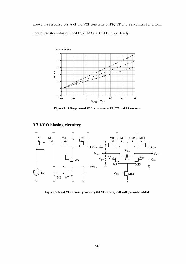
3.3 VCO biasing circuitry .............................................................................. 56
3.4 VCO dummies ......................................................................................... 59
3.5 VCO differential-to-single converter ....................................................... 63
3.6 Simulation Results ................................................................................... 64
3.7 Comparison to Previously Published Works ........................................... 68
3.8 Coarse tuning and fine tuning VCO ......................................................... 70
3.9 Complex compensation ............................................................................ 71
Chapter 4 Design of the PLL System ........................................................................ 72
4.1 Overview .................................................................................................. 72
4.2 Phase Frequency Detector Design ........................................................... 75
4.3 Charge Pump Design ............................................................................... 78
4.4 Feedback divider ...................................................................................... 81
Page 8
v
4.5 Other building blocks ............................................................................... 82
4.6 System modeling ...................................................................................... 84
4.7 PLL simulation results with and without VCO compensation ................ 85
4.8 Comparison of PLL performance with prior arts ..................................... 89
Chapter 5 Conclusion and Recommendations ........................................................... 94
5.1 Conclusion ............................................................................................... 94
5.2 Recommendations for further research .................................................... 97
Author’s Publications ................................................................................................. 99
Bibliography ............................................................................................................ 100
Appendices ............................................................................................................... 111
A.1 Product matrix of general purpose and clock generator PLLs .............. 111
A.2 Design Information ............................................................................... 113
Page 9
vi
Summary
Phase lock loops (PLLs) are used to multiply low-frequency clocks to generate
clocks that are of high frequency to be used for on-chip synchronous circuits. There
has been a constant demand for CMOS general purpose or clock generation PLLs for
synchronous chip operation in low (tens ~hundreds of MHz), mid (hundreds ~over
GHz) and high (hundreds ~several GHz) frequency ranges. Typical fabless
companies would pay royalties per wafer/die or one time charge to make use of such
PLLs in 0.25µm~28nm CMOS processes provided by major foundries (TSMC,
UMC and GLOBALFOUNDRIES). Voltage-controlled oscillator (VCO) is an
essential building block for PLLs. Due to the manufacturing limitation and the
process variation in fabricating transistors, operating supply voltage and temperature
(PVT), the ratio of the VCO frequency at the fastest condition to the slowest
condition could change by a factor of 2~3 or even more. As such, significant
variation of VCO gain is expected, corresponding to a significant spread in
bandwidth for the PLL operation. For the same targeted VCO frequency, the loop
bandwidth and stability of the PLL could thus vary greatly due to the variation in the
VCO gain across PVT conditions. Also, the upper bound of the usable frequency
range is limited to that of the slowest running condition within the tuning voltage
range while the lower bound of the usable frequency range would normally be bound
by the fastest running condition. This kind of undesired variation limits the designer
as he has to design for sub-optimal performance with conservative design parameters
to ensure functionality of the PLL for all PVT possibilities.
This thesis proposes a VCO compensation technique that could reduce the VCO’s
frequency variation across different PVT conditions. The technique incorporates a
Page 10
vii
simple process variation detection circuit, a comparison circuit that generates digital
control codes to control the current that goes to the biasing circuitry of the VCO. The
compensation circuitry is of small area and does not consume significant extra power.
To verify the proposed compensation techniques in VCO design, a fully-integrated
PLL clock generator has been designed for 1GHz~3GHz general purpose clock
generation using IBM’s 0.13µm CMOS 8RF process. With proper selection of the
compensation currents (and resistors), the usable frequency range could be extended
by a factor of 1.45. For the same targeted frequency, the variation of the
compensated KVCO is slightly above 10% at most, reduced from a high value of 60%
without compensation. Overall, the bandwidth variation is reduced by a factor of 1.7
from 2.2 for a PLL with compensated VCO, for the whole frequency tuning range,
across all the PVT variation from -40°C to 125°C. Specifically, for the same targeted
frequency, the KVCO variation has been reduced from a factor of 1.6 to about 1.1. For
the same target frequency, the maximum variation in damping factor has been
reduced from about 1.3 to slightly over 1.05. The frequency variation with respect to
the same control voltage is reduced to ±3.9% across all the PVT variation from -
40°C to 125°C.
VCO dummies are normally added to the VCO in order to provide a uniform loading
for each VCO delay stage. To check the impacts of different VCO dummy
implementation on PLL jitter, five experimental charge pump PLLs are simulated
with difference only in the dummy stages: (i) no dummy, (ii) simple dummy, (iii)
single stage differential dummy, (iv) double stage differential dummy and (v) full
differential dummy with the D2S converters. The simulation result shows that with
the improved symmetry, the noise contributed by the fluctuation in the VCO bias
would have been suppressed correspondingly. As a result, the PLL output clock jitter
Page 11
viii
could be reduced by increasing the symmetry in the VCO dummies. However, there
is a tradeoff for the jitter performance with the power consumption and silicon area.
The PLL designed was simulated with five different loop bandwidths achieved by
varying the charge pump currents and a minimum point with best jitter performance
is identify to verify the performance of the VCO with compensation. Simulation at
the SS and FF corners shows that the jitter performance of the PLL employing
compensated VCO is improved compared to the conventional design without VCO
compensation. The PLL output frequency range is also shown to be widened due to
the extended usable VCO frequency range.
The PLL is simulated for clock generation at 1GHz, 1.4GHz, 2GHz, 2.56GHz and
2.88GHz with the simple dummy and the full dummy configuration, respectively.
The long term periodic jitter (simulated with 50k cycles) and power consumption of
the designed PLL is compared with the published prior arts that were designed for
low jitter and low power clock generation at 1GHz, 1.4GHz and 2GHz. The tradeoff
in power consumption and jitter performance of the PLL designed is observed. A low
jitter and low power PLL that could be used for general purpose clock generation has
been achieved. The simulated jitter and power consumption of the designed PLL is
shown to be comparable/better than the prior arts used for comparison. The peak-to-
peak long term period jitter (simulated by using the eye diagram composed of 50k
cycles of the PLL output clock) achieved is close to or below 2% of the clock period.
Page 12
ix
List of Figures
Figure 1-1 Variation of VCO frequency due to process and temperature ................... 2
Figure 1-2 Variation of VCO gain due to process and temperature ............................ 3
Figure 1-3 (a) Variation of normalised VCO gain due to process and temperature
(b)Variation of normalised damping factor due to process and temperature ............... 3
Figure 2-1 Basic PLL ................................................................................................... 9
Figure 2-2 Block diagram of a ADPLL ..................................................................... 10
Figure 2-3 A charge pump PLL ................................................................................. 11
Figure 2-4 The 3-state diagram of PFD ..................................................................... 12
Figure 2-5 Operation of a PFD .................................................................................. 12
Figure 2-6 PFD (a)with dead zone (b)ideal and without dead zone .......................... 13
Figure 2-7 (a) Charge pump (b) timing mismatch of UP’ and DN (c) timing balance
by inserting a pass gate .......................................................................................... 15
Figure 2-8 (a) Charge pump OFF (b) Charge sharing (c) Bootstrapping .................. 16
Figure 2-9 Linear model of a CMOS ring Oscillator ................................................. 18
Figure 2-10 (a) Four-stage differential VCO (b) Simple differential stage ............... 20
Figure 2-11 (a) Manetis delay cell (b) Hong Park delay cell (c) Lee-Kim delay cell 21
Figure 2-12 Linear model of a charge pump PLL ..................................................... 23
Figure 2-13 Noise contribution in a linear PLL model .............................................. 24
Figure 2-14 (a)Gain and phase plots of the open loop transfer function, third order (b)
gain and phase plots of the open loop transfer function, second order (ignore CP) ... 26
Figure 2-15 Magnitude of noise transfer function, an example ................................. 29
Figure 2-16 Block diagram of supply-regulated PLL ................................................ 30
Figure 2-17 Block diagram of a PLL with supply-noise cancellation ....................... 31
Figure 2-18 VCO with noise-cancelling circuit ......................................................... 31
Page 13
x
Figure 2-19 Compensated clock buffer ...................................................................... 31
Figure 2-20 (a) VCO with supply-noise compensation (b) VCO delay cell .............. 32
Figure 2-21 PLL with on-chip calibration ................................................................. 33
Figure 2-22 Block diagram of self-biased PLL ......................................................... 35
Figure 2-23 VCO circuits of the self-biased PLL ...................................................... 35
Figure 2-24 Charge-pump PLL implemented with sample-reset technique .............. 37
Figure 2-25 Gain compensation VCO ....................................................................... 38
Figure 2-26 PLL with VCO calibration block ........................................................... 39
Figure 2-27 (a) VCO delay cells (b) VCO calibration block ..................................... 39
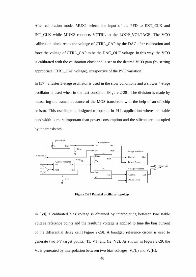
Figure 2-28 Parallel oscillator topology .................................................................... 40
Figure 2-29 Calibration bias generation circuit ......................................................... 41
Figure 2-30 PLL with self-calibrated VCO ............................................................... 41
Figure 2-31 Temperature and process compensated VCO ........................................ 42
Figure 3-1 Conventional VCO design ....................................................................... 46
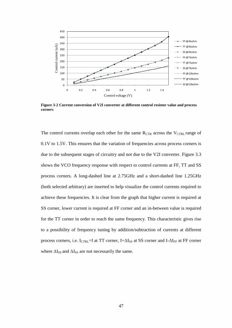
Figure 3-2 Current conversion of V2I converter at different control resistor value and
process corners ........................................................................................................... 47
Figure 3-3 Variation of VCO frequency with respect to control currents ................. 48
Figure 3-4 Variation of VCO frequency versus control resistance ............................ 48
Figure 3-5 Determine the compensating resistance and current required .................. 49
Figure 3-6 The VCO design ....................................................................................... 50
Figure 3-7 Comparator design ................................................................................... 53
Figure 3-8 Block diagram of the compensation detection circuitry .......................... 53
Figure 3-9 (a) Process corner detection circuit (b) Detected voltage across
temperature range of -40°C to 125°C ........................................................................ 55
Page 14
xi
Figure 3-10 Response of compensation detection circuitry with respect to detected
voltage ........................................................................................................................ 55
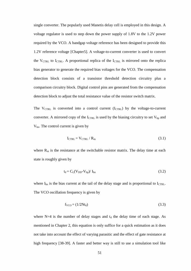
Figure 3-11 Response of V2I converter at FF, TT and SS corners ............................ 56
Figure 3-12 (a) VCO biasing circuitry (b) VCO delay cell with parasitic added ...... 56
Figure 3-13 Voltage-to-current (V2I) converter ........................................................ 57
Figure 3-14 Frequency response of the PLL with different V2I ............................... 58
Figure 3-15 Vbn of the VCO for V2I with different stability ..................................... 58
Figure 3-16 VCO with full differential dummies ...................................................... 59
Figure 3-17 (a) Simple dummy, (b) single stage differential dummy, (c) double stage
differential dummy ..................................................................................................... 59
Figure 3-18 Open loop VCO biasing voltages with simple dummies and full
dummies ..................................................................................................................... 60
Figure 3-19 Closed loop VCO biasing voltages with simple dummies and full
dummies ..................................................................................................................... 61
Figure 3-20 Circuit diagram of the differential-to-single converter .......................... 63
Figure 3-21 (a) Variation of VCO frequency without compensation (b) Variation of
VCO frequency with compensation ........................................................................... 64
Figure 3-22 (a) Variation of VCO gain without compensation (b) Variation of VCO
gain with compensation ............................................................................................. 65
Figure 3-23 (a) Normalised bandwidth with respect to VCO frequency without
compensation (b)normalised bandwidth with respect to VCO frequency with
compensation ............................................................................................................. 67
Figure 3-24 (a) Normalised damping factor with respect to VCO frequency without
compensation (b) normalised damping factor with respect to VCO frequency with
compensation ............................................................................................................. 67
Page 15
xii
Figure 3-25 Coarse tuning and fine tuning VCO ....................................................... 70
Figure 3-26 Complex compensation .......................................................................... 71
Figure 4-1 Block diagram of the PLL ........................................................................ 72
Figure 4-2 Circuitry of the PFD design ..................................................................... 75
Figure 4-3 (a) Level shifter design (b) Flip Flop schematics used in the PFD .......... 75
Figure 4-4 Feedback Clock runs faster than reference clock. DN pulse indicates that
the feedback clock needs to slow down ..................................................................... 77
Figure 4-5 Feedback clock runs slower than reference clock. UP pulse indicates that
the feedback clock needs to run faster. ...................................................................... 77
Figure 4-6 Simplified circuitry of the charge pump .................................................. 79
Figure 4-7 Current mismatch with ICP at 60µA, (a) VDD=1.8V, (b) VDD=1.68V... 80
Figure 4-8 (a) A divide-by-32 feedback divider consists of five ½ divider (b) a ½
divider ........................................................................................................................ 81
Figure 4-9 Bandgap-reference voltage generator ...................................................... 82
Figure 4-10 Band-gap based accurate reference current generator ........................... 83
Figure 4-11 Voltage regulator .................................................................................... 83
Figure 4-12 (a) System behaviour modelling (b) loop filter ...................................... 84
Figure 4-13 Transient plots of control voltage for varying charge pump currents .... 85
Figure 4-14 Transient plots of the control voltage for the PLL at 2.56GHz ............. 87
Figure 4-15 Long term period jitter with loop bandwidth of 2.69MHz for clock
outputs at (a)2GHz, (b)2.56GHz, (c)2.88GHz ........................................................... 92
Page 16
xiii
List of Tables
Table 2-1 Classification of PLLs ................................................................................. 9
Table 3-1 An example for compensated control resistor and compensation currents 50
Table 3-2 Resistor value ............................................................................................ 54
Table 3-3 The effects of dummy on the PLL output clock jitter (10k cycles) ........... 61
Table 3-4 Comparison of different VCOs ................................................................. 69
Table 4-1 Current mismatch window at ICP of 60µA ................................................ 81
Table 4-2 The effects of varying charge pump current on the PLL output clock jitter
at 2.56GHz (10k cycles) ............................................................................................ 86
Table 4-3 The PLL output clock jitter at 2.56GHz with and without compensated
VCO (10k cycles) ...................................................................................................... 87
Table 4-4 Comparison of PLL Performance without normalization ......................... 89
Table 4-5 The better jitter performance with higher bandwidth ................................ 91
Table 4-6 Comparison of PLL Performance with normalization .............................. 93
Table A-1 Design Information ................................................................................. 113
Page 17
1
Chapter 1
Introduction
1.1 Motivation
Phase locked loops (PLLs) are used to multiply low-frequency clocks from off-chip
to generate clocks that are of high frequency to be used on-chip. There has been a
constant demand for CMOS general purpose or clock generation PLLs for
synchronous chip operation. Such PLLs come in the frequency range of low-range
(10-100’s MHz), mid-range (100s MHz - GHz) and the high-range (100sMHz -
several GHz). True Circuits Inc. is one company who provides CMOS PLLs that
span technology nodes in 0.25µm~28nm to major foundries (TSMC, UMC and
GLOBALFOUNDRIES) [Appendix A.1]. This work aims to design a high frequency
range (1GHz-3GHz) clock generation PLL that could provide wide output frequency
range, low power consumption and low jitter performance. The voltage-controlled
oscillator (VCO) is an essential circuit for PLLs. Due to the variation of transistors
and other passive elements in the manufacturing process, operating supply voltage
and temperature (PVT), the ratio of the VCO frequency at the fastest condition to the
slowest condition could vary by a factor of 2~3 or even more [1, 2]. As such,
significant variation of VCO gain is expected, corresponding to the same scale of
spread in bandwidth for the PLL. For the same targeted VCO frequency, the loop
bandwidth and stability of the PLL could thus vary greatly due to the variation in the
VCO gain. Figure 1-1 shows how the frequency of a conventional VCO varies with
respect to the control voltage (VCTRL), from the fastest running process corner (FF) at
-40°C to the slowest running process corner (SS) at 125°C. The frequency of the
Page 18
2
VCO in nominal process corner or the typical process corner (TT) would be bounded
by the FF and SS corners. With this variation, the upper bound of the usable
frequency range is limited to that of the slowest running condition within the tuning
voltage range, as indicated by the horizontal dashed line in Figure 1-1. The lower
limit would normally be bound by the fastest running condition. It is clear that for the
same control voltage, the fastest running frequency is more than 30% higher than the
slowest one. The VCO gain (KVCO), could vary by more than 60% for the same target
frequency, as shown in Figure 1-2. The normalised bandwidth (with respect to the
lowest bandwidth in the range) shows that the PLL loop bandwidth could vary by
more than 60%, as shown in Figure 1-3(a). The normalised damping factor (with
respect to the lowest damping factor) for the PLL could vary by 30%, as shown in
Figure 1-3(b).
Figure 1-1 Variation of VCO frequency due to process and temperature
0.0
0.5
1.0
1.5
2.0
2.5
3.0
0.0 0.2 0.4 0.6 0.8 1.0 1.2 1.4
VC
O fr
equen
cy (
GH
z)
Control voltage(V)
FF -40 degree-C
TT 25 degree-C
SS 125 degree-C
FF 25 degree-C
SS 25 degree-C
upper usable frequency
Page 19
3
Figure 1-2 Variation of VCO gain due to process and temperature
Figure 1-3 (a) Variation of normalised VCO gain due to process and temperature
(b)Variation of normalised damping factor due to process and temperature
Due to the sampling nature of a PLL, a common rule of thumb is to design the loop
bandwidth (ωBW) to be less than 1/10 of the reference frequency. Loop bandwidth is
proportional to KVCO so the bandwidth selected must satisfy the highest KVCO (FF
corner) for a targeted frequency. The damping factor is proportional to the square
root of KVCO, so the design has to cater for the lowest KVCO (SS corner) to maintain a
minimum damping factor. For a given charge pump current and divider ratio, the
resistor and the capacitor values have to be selected based on the lowest possibly
0.80
1.00
1.20
1.40
1.60
1.80
2.00
0.6 1.1 1.6 2.1 2.6 3.1
VC
O g
ain (
GH
z/V
)
VCO frequency (GHz)
FF -40 degree-C
TT 25 degree-C
SS 125 degree-C
FF 25 degree-C
SS 25 degree-C
0.60
0.80
1.00
1.20
1.40
1.60
1.80
2.00
2.20
0.7 1.2 1.7 2.2 2.7
No
rmalise
d b
and
wid
th
VCO frequency (GHz)
FF -40 degree-C
TT 25 degree-C
SS 125 degree-C
0.80
0.90
1.00
1.10
1.20
1.30
1.40
1.50
0.7 1.2 1.7 2.2 2.7
No
rmalise
d
dam
pin
g f
acto
r
VCO frequency (GHz)
FF -40 degree-C
TT 25 degree-C
SS 125 degree-C
Page 20
4
KVCO at the slowest running condition. This could mean a more conservative
selection of resistor and capacitor, i.e. larger sizes of resistor and capacitor in the
loop filter. Also, it is known that the output phase noise of a PLL associated with the
VCO can be reduced by increasing the loop bandwidth. In contrast, a smaller
bandwidth is desired in order to filter out the noise that comes from the reference
clock. As such, there is an optimum loop bandwidth trading off between these two
noise sources. With all these design constraints and the variation in KVCO, a designer
is left with limited choices of design margins and more conservative design
parameters that guarantee functionality and stability for all possible PVT variation,
but at sub-optimal performance. For example, the bandwidth is selected based on the
worst-case condition, i.e. the fastest condition, trading off for less optimal
bandwidths at other conditions. There is a class of complicated adaptive bandwidth
PLL design [1] targeting PVT tolerance on loop bandwidth and damping factors by
means of cancelling each other out in the equations or by complex calibration
techniques. Nevertheless, a VCO with less variation in KVCO is still beneficial as it
helps to design PLL with a narrower range of loop bandwidths as well as the
damping factors, apart from the wider tuning range. In this study, the design of a
compensation scheme to improve the PVT tolerance of differential VCO is described.
A four-stage differential ring oscillator with voltage regulation is employed to
achieve the voltage tolerance. Depending on the process corner and temperature, the
proposed compensation scheme works by increasing or decreasing the control
current accordingly, thereby maintaining the desired frequency. This research focus
on an on-chip compensation technique which adjusts the current going to the VCO
depending on the process and temperature conditions detected. A charge pump PLL
is implemented with this VCO, demonstrating desired advantages as compared to a
Page 21
5
conventional VCO without compensation. The different VCO dummy configuration
is also explored to determine the lowest jitter design approach.
1.2 Objectives
The major objective of this study is to explore techniques in reducing the effect of
PVT variation of VCO on a general purpose clock generator that could be used for
the frequencies range of 1GHz to 3GHz. The focus of this research is on the
compensation techniques for reducing the frequency and gain variation of a VCO
across different PVT corners. With this compensated VCO, a PLL could be designed
with relatively constant voltage gain, bandwidth and stability. A relatively optimum
jitter performance at a targeted frequency is also made possible with this design
technique for process shift to SS and FF corners.
The next objective of the study is to determine ways to make use of the compensated
VCO in reducing the output clock jitter of the PLL. A way to make use of the
symmetry in the VCO dummy stages to reduce jitter is also explored. Lastly but not
the least, the PLLs are designed to achieve low power and low jitter performance that
could be readily employed for the general purpose clock generation usage.
1.3 Major contribution of the Thesis
A compensated VCO with improved PVT tolerance has been designed. For the same
target VCO frequency, the loop bandwidth and stability could thus vary greatly due
to the variation in the VCO gain. By detecting the threshold voltage due to process
variation, the control current to the VCO is adjusted accordingly so that the VCO
Page 22
6
frequency variation across PVT corners is greatly reduced. The variation of
frequency at 25°C is within ± 0.6% for the tuning voltage range from 0.4V to 1.5V
comparing the fastest to slowest conditions. The variation of frequency at each
control voltage point is within ±3.9% across a temperature range of -40°C to 125°C.
Overall, the usable frequency range of the compensated VCO has been extended by a
factor of 1.4. The VCO sensitivity to power supply noise is reduced by always
running the VCO with 1.2V which is generated from a bandgap-based 1.8V voltage
regulator. A fully on-chip integrated charge pump PLL clock generator has been
designed with this compensated VCO, demonstrating desired advantages as
compared to a conventional VCO without compensation. A relatively invariant loop
bandwidth and stable PLL has been designed with such VCO compensation
techniques. Comparison shows that the proposed VCO compensation technique is
indeed better than the prior arts.
Five experimental charge pump PLLs are simulated with difference only in the
dummy stages: (i) no dummy, (ii) simple dummy, (iii) single stage differential
dummy, (iv) double stage differential dummy and (v) full differential dummy with
the D2S converters. The simulation results show that with the improved symmetry,
the noise due to fluctuation in the VCO bias could be suppressed correspondingly.
As a result, the PLL clock jitter has been reduced by increasing the symmetry in the
VCO dummies. Of course, this comes with a tradeoff with increased power
consumption and silicon area.
The PLL designed was simulated with five different loop bandwidths, by varying the
charge pump currents and a minimum point with best jitter performance is identified
to verify the performance of the VCO with compensation. Simulation at the SS and
FF corners shows that the jitter performance of the PLL is improved compared to the
Page 23
7
conventional design without VCO compensation. The PLL output frequency range is
also shown to be widened up due to the extended usable VCO frequency range.
The PLL is simulated for clock generation at 1GHz, 1.4GHz, 2GHz, 2.56GHz and
2.88GHz with the simple dummy and the full dummy, respectively. The long term
periodic jitter (simulated with 50khits) and power consumption of the designed PLL
is compared with the published prior arts that were designed for low jitter and low
power clock generation at 1GHz, 1.4GHz and 2GHz. The simulated jitter and power
consumption of the designed PLL is shown to be comparable/better than these prior
arts. A low jitter and low power PLL that could be used for general purpose clock
generation has thus been achieved.
1.4 Organization of the Thesis
This thesis is divided into five chapters. This first chapter provides an overview, the
motivation, the major contribution and the organization of the thesis. In Chapter 2, a
review of the PLL design topics in particular the charge pump PLL is presented.
Various design challenges for the building blocks and the loop characteristics are
described. In Chapter 3, the focus of this research, i.e. the issues of the PVT variation
to VCO and hence the PLL performance, are described in details and the proposed
compensation techniques are presented. The circuit level schematics of the proposed
techniques and the simulation results are compared with prior arts. In Chapter 4, the
complete PLL design and the simulation results are presented. The building blocks
are described and the simulation results presented. Lastly, the thesis is summarised
and concluded in Chapter 5. The potential future works to be further explored and
improve on the current work are also recommended in the last section.
Page 24
8
Chapter 2
Fundamentals of the PLL
The idea of PLL was introduced in the last century, for synchronous radio detection
by H.de Bellescize in France [3]. It was developed then as an alternative to American
engineer E. Armstrong's superheterodyne receiver architecture for radio
communication. PLLs have many applications. They can be used for narrow
bandwidth filter, clock-and-data recovery, skew reduction in digital system, internal
clock generation that is locked to an external reference clock, frequency synthesis to
generate a stable periodic signal, frequency modulation and demodulation on a
carrier. This chapter provides an overview of a PLL system. The basic definition of
various PLL systems is presented in Section 2.1. Section 2.2 provides a detailed
review of the charge-pump PLL [4] system which is the topic for study throughout
this thesis. Some state-of-the-art charge pump PLLs are briefly reviewed in Section
2.3. A brief comment on the performance of different schemes of PLL system with
respect to PVT variation is presented in Section2.4.
2.1 Basic PLL Definition
A basic PLL [Figure 2.1] consists of three essential elements: a phase detector (PD),
a loop filter (LF), and a voltage-controlled oscillator (VCO) [5]. A PLL behaves as a
feedback system which compares the input and output phases. A periodic input
signal (Vin) is compared against the VCO output signal (Vout) by the phase detector
(PD). The output of the PD is an error voltage (VPD) proportional to the phase
difference of Vin and Vout, i.e. Φin-Φout. VPD is then filtered by the loop filter so that
the dc component of it is passed on to control the VCO. The control voltage (VCTRL)
Page 25
9
varies the VCO frequency until the phases are aligned, i.e. the PLL loop is locked.
When locked, the Vout still has a small phase error as compared to Vin but the average
VCO frequency equals to the average frequency of Vin.
Figure 2-1 Basic PLL
Based on the definition given by Roland E. Best [6], PLLs can be classified into
linear PLL(LPLL), digital PLL(DPLL), all-digital PLL(ADPLL) and software
PLL(SPLL). In the LPLL, an analog multiplier is used as the PD, the LF consists of a
passive or active RC filter and a VCO. A DPLL is indeed a hybrid device in which
the PD is built from a digital circuit but the remaining blocks remain analog. The
ADPLL is exclusively consists of digital functional blocks. The SPLL is normally
implemented by a hardware platform such as a digital signal processor (DSP) such
that the PLL function is realized purely by software. Nikolas [7] classifies the PLLs
into three general categories: analog PLL, hybrid PLL, digital PLL based on their
implementation. Table 2-1 summarises the classification of PLLs based on the
definition given in [6-7], with respect to PD, LF and oscillator.
Table 2-1 Classification of PLLs
[6] [7] PD LF Oscillator
Linear PLL Analog PLL Analog Resistor, capacitor Voltage controlled
Digital PLL Hybrid PLL Digital Resistor, capacitor Voltage controlled
All digital PLL Digital PLL Digital Digital Digitally Controlled
Software PLL Digital PLL Software Software Software
LFPD
Phase LoopDetector Filter VCO
VoutVin
ΦoutΦin
VPD VCTRL
Page 26
10
Based on the classification defined by [6-7], the charge pump PLL is a digital/hybrid
PLL. To avoid confusion with the ADPLL, the charge pump PLL is defined to be a
hybrid PLL throughout this thesis.
Figure 2-2 Block diagram of a ADPLL
An ADPLL [Figure 2-2] consists of a time-to-digital converter (TDC), a digital loop
filter (DLF), a digitally controlled oscillator (DCO), and a feedback divider [8-9].
The TDC detects the phase difference from the reference clock (RefClk) and the
feedback clock (FbClk), and converts it into a digital word proportionally. The DLF
filters this data digitally and generates a set of control code to control the DCO. The
DLF is a proportional-integral filter realizing the Type-II PLL response.
Traditionally, a digital-to-analog converter (DAC) interfaces the DLF to the voltage
controlled oscillator (VCO) [10-11]. An alternate approach is to employ a digitized
mechanism to vary the frequency in an LC-tank based VCO [12] or inverter-ring
oscillator DCO [13]. The simplest TDC is based on a delay line composed of buffers,
each with a delay time of TDEL[14]. The resolution of such TDC is limited by the
TDEL of each individual inverter, while the detectable range is proportional to the
number of delay stages[15]. To achieve finer resolution, methods using Vernier delay
line based on difference of delay chains [15-16], scrambling TDC by averaging many
consecutive cycles[17] have been developed. A different approach from the TDCs
mentioned, is to use a bang-bang phase detector (!!PD) as a 1-bit TDC for its
DLFTDC
DCO
RefClk
FbClk
Clkout
/ N
Page 27
11
simplicity [13]. The advantages of the bang-bang phase detector, due to its simplicity
and accuracy, exceeds the drawback of nonlinearity and noise in the multi-Gbps
regime [18].
Figure 2-3 A charge pump PLL
2.2 Charge Pump PLL and its components
The basic concept of a PLL system and the phase locking operation has been
described in Section 2.1. In this section, the basic charge pump PLL and its
components are discussed. The block diagram of a basic charge pump PLL is as
shown in Figure 2.3. It consists of a phase-frequency detector (PFD), a charge pump
(CP), a loop filter (LF), a voltage-controlled oscillator (VCO) and a feedback divider
(FBDIV). When locked, the frequency of Clkout is N times the frequency of RefClk.
The function and operation of each block is described below.
2.2.1 Phase Frequency Detector
A common PFD block is as shown in Figure 2.3, acting as a functional block that
receives two input clock signals and producing control signals that cause the charge
pump to perform charging or discharging operation. A PD is insensitive to the
frequency differences and may fail to lock when the frequency of the feedback signal
is far from the reference signal. This inadequacy in the lock acquisition range can be
remedy by using “aided acquisition” whereby the frequency detection is included.
D
D QR
D Q
RRefClk
FbClk
Delay DN
UP
/ N
Phase Frequency Detector Charge Pump
Feedback Divider
VCO
Loop Filter
RZ
CP CR
VCTRLClkout
Page 28
12
This is achieved by a PFD which detects both the phase and frequency differences.
The PFD outputs are denoted UP and DN (down) respectively. The RefClk denotes
the reference clock whereas FbClk denotes the feedback clock. Both UP and DN are
initially low in State 0. A rising edge of RefClk input causes the UP signal to go high
(State I). This indicates that the FbClk needs to be increased, i.e. the VCO needs to
run faster in order to match the input reference clock. When the FbClk leads the
RefClk and goes high, the DN signals goes to high (State II). This means that the
FbClk needs to run slower. When both RefClk and FbClk go high simultaneously,
the NAND gate is set low and resets the PFD to the zero state, after passing through
a delay stage. In this way, the PFD behaves as a three-state device. Figure 2.4 is a
state diagram that depicts the 3-state behavior of a PFD.
Figure 2-4 The 3-state diagram of PFD
Figure 2-5 Operation of a PFD
Figure 2.5 shows the operation of a PFD and reflects the 3-state behavior. Initially,
both the frequency and phase of the RefClk and FbClk are not matched. As RefClk
leads FbClk, the UP signal is generated to have a faster FbClk (State I). In the
adjustment process, FbClk may become leading the RefClk and a DN signal is
FbClk
RefClk
RefClk
RefClk
FbClk
UP=0DN=1
UP=0DN=0
UP=1DN=0
State 0 State I
FbClk
State II
locked
FbClk
RefClk
UP
DN
Φref ≠Φfbfref ≠ffb
glitch
Page 29
13
generated (State II). Ideally, when a UP pulse is generated, the DN signal should
stay flat but in real case, a glitch of DN occurs. The opposite is also true when a DN
pulse is generated. The glitch is alright as long as it is short and quick such that the
charge pump does not respond to it. The adjustment continues until the phase of
FbClk is aligned to the RefClk and their frequency becomes equal. In this stage, the
PLL is said to be in “locked” condition.
Figure 2-6 PFD (a)with dead zone (b)ideal and without dead zone
Dead zone occurs when the loop does not respond to small phase errors at PFD
inputs [Figure 2.6]. This causes undesired jitter and phase noise at the output clock.
There is a limited amount of pulses that the PFD can generate. Also, the charge-
pump cannot be turned on and off in such a narrow time frame. A delay is normally
introduced in the reset path in order to guarantee a minimum pulse width that
remedies the dead-zone problem. However, widening the reset pulse increases the
time where both UP and DN are high and the charge pump conducts simultaneously.
This has undesired effect on the VCO control voltage and phase noise. If the
dynamic flip flops (DFFs) are not properly matched and that one reset is faster than
the other, the reset signal will be pulled to low and not able to reset the slower DFF.
Φref - Φfb Φref - Φfb
VUP -VDN VUP -VDN
-2π +2π-2π +2πΦdeadzone
Page 30
14
2.2.2 Charge Pump
The charge pump (CP) circuit has two switches that are controlled by the UP and DN
signals from the PFD. The charge pump then pumps current pulses that either add or
remove charges from the loop filter capacitor (CCP). In this sense, the CCP converts a
digital signal (the PFD phase error) to an analogue signal (charge). The combination
of charge-pump and the capacitor CCP acts as an integrator that generates the average
of UP or DN pulses. The CP converts the phase difference to this average voltage
proportionally and feed into the VCO to adjust the frequency.
A linear continuous-time approximation is often used to model the simple charge
pump PLL. The error due to approximation is negligible if the PLL band-width is
1/10 or smaller than the reference clock frequency [4]. The average current charging
or discharging the capacitor is given by IAVG=ICP x (ΦUP-ΦDN)/2π. There are four
main undesired effects which could cause reference spur and need careful
consideration [19-22]. These are (i) leakage current in the loop filter, (ii) timing skew
between the UP and DN signals, (iii) current mismatch in the charge up and down
current path, (iv) charge sharing. The leakage currents could come from the capacitor
of the loop filter, the charge pump itself. The gate leakage would readily manifest
itself if MOS capacitor is incorporated in the loop filter design [23]. When the charge
pump is in off state, the leakage current could discharge the loop filter. This drain off
the current from the loop filter causing a phase offset. Gate leakage current is
becoming more significant as the technology continues to shrink and as the gate
dielectric thickness reduces.
Page 31
15
Figure 2-7 (a) Charge pump (b) timing mismatch of UP’ and DN (c) timing balance by inserting
a pass gate
Figure 2.7 shows the mechanism of the timing mismatch and its effect. As mentioned
in the Section 2.21, the dead-zone issue could be fixed by putting a delay in the reset
path of the PFD. This forces the UP and DN signals of the PFD to be “on”
simultaneously for a short period in each cycle when the PLL is in lock condition.
For a conventional charge pump, the UP signal is inverted to generate UP’ to turn on
the charging current as the PMOS transistor switch is active low. This introduces a
mismatch in the pulse arrival time for the UP’ and DN. A periodic disturbance to the
control voltage is thus generated and causes reference spur in the VCO output. One
possible ways to get rid of this mismatch is by inserting a transmission gate in the
DN control path. The delayed signal DN’ should arrive with negligible skew with the
UP signal provided the transmission gate is sized properly. The issue of current
mismatch could still occur even with the UP and DN’ signals aligned perfectly [19-
21, 24]. The current mismatch varies with the control voltage due to the finite output
impedance of the CMOS current source. This current mismatch also generates a
phase offset which contributes to the spur of the PLL output. The contributions to the
phase offset by the leakage current, timing mismatch and the current mismatch in the
charge pump is expressed as [20, 24]
Φε = 2𝜋 Ileak
ICP+
Δton
Tref
Δtd
Tref+
Δton
Tref
Δi
Icp [𝑟𝑎𝑑] (2.1)
D QR
D Q
RRefClk
FbClk
Delay
DN
UP
Vctrl
DN
UP
Vctrl
UP'
DN'
IUP
IDN
DN
UP'
IUP
UP'
IDN
Inet
VCTRL
Page 32
16
where Φε, Ileak, ICP, Δton, Tref, Δtd, Δi are the phase offset, the leakage current, the
charge pump current, the turn on time of the PFD, the reference clock period, the
delay mismatch, and the current mismatch of the charge pump, respectively. The
Δtd is much smaller than the Δton for this expression to be valid. The reference
spur in a 3rd
-order PLL is given approximately by [20, 24]
Pr = 20𝑙𝑜𝑔 2 𝐼𝐶𝑃 𝑅 2𝜋 Φ𝜀𝐾𝑉𝐶𝑂
2fref − 20𝑙𝑜𝑔
𝑓𝑟𝑒𝑓
𝑓𝑃1 [𝑑𝐵𝑐] (2.2)
where R denotes the resistor value in the loop filter, KVCO denotes the VCO gain, fref
denotes the reference frequency of the PFD and fP1 denotes the frequency of the pole
in the loop filter. Equation (2.1) and (2.2) imply that Δton, Δi should be reduced to
minimize the phase offset, as Δtd is much smaller than the Δton and Ileak is more due to
the process constraint. Nevertheless, Δton is required to get rid of the dead-zone issue.
With these observations, it is obvious that the current mismatch should be reduced as
much as possible. The deterministic jitter, Δdet, can be estimated from the reference
spur based on Fourier series analysis [25-26] and is given by an expression
Δdet = Tout 10𝑆𝑝𝑢𝑟 (𝑑𝐵𝑐 ) 20 (2.3)
where Tout is the ideal output period, Spur is the level of the reference spur in unit of
dBc.
Figure 2-8 (a) Charge pump OFF (b) Charge sharing (c) Bootstrapping
Vctrl
Cpu
Cpd
Vctrl
Cpu
Cpd
X
Y Y
Xt
Vctrl
VX
VY Y
X
VDD VDD VDD
Page 33
17
Charge redistribution occurs when charge pump move from the OFF to ON state. As
shown in Figure 2.8(a), when the charge pump switches are turned off, the voltage at
node X (VX) is discharged to ground through the parasitic capacitance Cpd and the
voltage at node Y (VY) is charged to VDD through the parasitic capacitance Cpu.
When the charge pump switches are turned on again, VY drops and the VX increases
and eventually VX≈VY≈VCTRL [Figure 2.8(b)]. This charge redistribution effect is
undesired as it causes a voltage jump in VCTRL. A bootstrapping technique can be
used to reduce this charge sharing effect [19-20, 27, 28]. A unity-gain amplifier is
used to hold node X and node Y at a potential equal to VCTRL when they are not
switched to VCTRL. When the switches are turned on again, the node X and node Y
start with a potential that is equal to the VCTRL as from the previous phase
comparison stage. In this way, the charge sharing between the loop filter and the
parasitic capacitances is avoided.
2.2.3 Voltage-Controlled Oscillator
Voltage-controlled oscillator (VCO) is the most critical component in a PLL. As its
name suggests, a VCO generates a periodic signal with a frequency that depends
linearly on the input control voltage (VCTRL) and eventually achieve the phase-locked
state. A CMOS VCO could be implemented with ring oscillators, relaxation circuits,
and LC resonant circuit. In a LC oscillator, a variable capacitor is typically employed
to tune the frequency given by 1/(2π√LC). The LC oscillator demonstrates the best
phase noise performance [29]. However, the ring oscillator has the advantages of
area that is more compact, less design complexity, wider tuning range that spans
orders of magnitude [30-31]. In today’s mixed-signal ICs, the ring oscillator has been
the most widely fabricated as compared to other oscillators. In this study, the ring
Page 34
18
oscillator VCO is used. Thus, the following sections focus review on CMOS ring
oscillator. There are two types of ring oscillators. One is based on the inverters and
the other is based on differential delay cells and is less susceptible to noise. The
advantages of CMOS based delay buffers are their simplicity, portable design and
their relaxed supply headroom requirements. Their main disadvantage is their high
control-voltage to delay gain which is typically 1% of delay per 1% of regulated
supply/control voltage.
The most basic ring oscillator design consists of a chain of single ended inverters. In
this configuration, a total odd number N of inverter stages is needed so that the
oscillator does not latch up at a DC level [19]. For stable oscillation, the gain
magnitude of the loop should be greater than or equal to one and the total phase
difference should fulfill the Barkhausen criterion, i.e. equal to a multiple of 2π [19,
32]. The two conventional criteria for oscillation is shown to be “necessary but not
always sufficient” for oscillators, due to the effects of parasitic elements [32]. As
such, the loop gain is typically chosen to be at least twice the required values [19].
With a linearised model [29, 33], the basic loop of the ring oscillator is redrawn in
Figure 2.9. R and C denote the output resistance and the capacitive load of each of
the delay stages; GmR denotes the gain required for a stable oscillation.
Figure 2-9 Linear model of a CMOS ring Oscillator
-Gm
R C
-Gm
R C
-Gm
R C
Φ=2π+2θΦ=π+θ Φ=Nπ+NθΦ=0
Page 35
19
A good explanation relating the phase, gain and oscillation frequency was provided
in [33] and is adapted here for illustration. The loop gain GL(s) is defined as
GL s = H1 s H2 s H3 s … HN s (2.4)
where HN(s) is the transfer function of each stage in the s-domain. In practice, the
gain of each stage is identical, i.e. H1(s) = H2(s) = H3(s) = HN(s) =H(s), such that
GL s = H(s)N (2.5)
To fulfill the Barkhausen criterion, each single stage should provide a phase shift of
2kπ/N at the unity gain frequency, where k is an integer. Thus, we have
∠𝐻 jω0 = 2kπ N (2.6)
|𝐻 jω0 |N = 1 (2.7)
Each stage has a phase shift of (π+θ), where π comes from the DC inversion and θ
from the RC load (frequency dependent phase shift). To minimize the required phase
shift and thus the number of delay stages, the total frequency dependent phase shift
should be equal to ±π, i.e. Nθ=±π. The transfer function and the phase of a single
stage at the oscillation frequency ω0 is given by
𝐻 jω0 =−Gm R
1+jω0RC (2.8)
∠𝐻 jω0 = −tan−1 ω0RC ± π (2.9)
The phase shift contributed by each stage is thus given by
θ = −tan−1 ω0RC (2.10)
and the oscillation frequency is given by
Page 36
20
ω0 =tan θ
RC (2.11)
The gain requirement is given by (2.7)
|𝐻 jω0 |N = Gm R
1+(ω0RC )2
N
= 1 (2.12)
With some derivation steps, the gain requirement is given by
Gm R ≥ 1 cos θ (2.13)
For a three-stage ring oscillator, the frequency and gain is thus calculated to be
√3/RC and 2 using (2.11) and (2.13) respectively, where θ=π/3.
Differential ring oscillators are preferred over the single-ended because of their better
immunity to power supply disturbance [31] and other inherent advantages like
improved spectral purity, better duty cycle and can be constructed with either
even/odd stage of delay cells. Some state of the arts PLL had been designed using
differential VCO with different classical differential delay cells are [30, 34-37]. For
an even stage differential VCO, the extra phase shift (π) can be obtained by
configuring one stage such that it does not invert [19]. Figure 2.10 shows a four-
stage differential VCO where the fourth and the first stage are not inverted.
Figure 2-10 (a) Four-stage differential VCO (b) Simple differential stage
Assuming each stage of a N-stage differential ring oscillator provides a delay of td,
then the period is 2NTd as the signal needs to go through each of the delay stages
Vcontrol
Vout+Vout-
Vin+ Vin-M3 M4
M1 M2
ISS
VDD
Page 37
21
twice to provide a period of oscillation [38-39]. The oscillation frequency is thus
given by
f = 1 2NTd (2.14)
The delay per stage can be expressed as CLVSW / ISS [30, 39] where CL is the load
capacitance of the delay stage, VSW the peak-to-peak voltage swing and ISS is the tail
current used in the delay stage, respectively. The oscillation frequency is given by
f =ISS
2NCL VSW (2.15)
This is only suffice for a quick estimation of the oscillation frequency while a more
comprehensive analytical equation is provided by [39] whereby the effect of varying
parasitic is included and the effect of gate resistance at high frequency is also being
considered. Important parameters in the VCO design are phase noise, jitter, centre
frequency, tuning range and linearity. For the monotonic relationship to be applied
over a large frequency range, the KVCO needs to be reasonably constant. Important
concerns in the design of low-jitter VCO are the variations of the output phase and
frequency as a result of noise on the control lines and the power supply.
Figure 2-11 (a) Manetis delay cell (b) Hong Park delay cell (c) Lee-Kim delay cell
Vout+
Vin+ Vin-
Vbp
Vbn
M1 M2 M3 M4
M5 M6
M7
Vin1+ Vin1-
M8 M9 M10 M11
M14 M15
Vin2+Vin2-
M12 M13
Vcont
A B
M16 M17
M20 M21
VconVcon
M18 M19
BAVout-
Page 38
22
Three classical differential delay cells, Manetis delay cell [34, 37], Hong Park delay
cell [36] and Lee-Kim delay cell [35] are as shown in Figure 2.11 (a), (b) and (c)
respectively. Manetis delay cell is perhaps by far the most popular differential delay
cell being studied and adapted. It consists of a pair of symmetric loads by diode-
connecting the PMOS device in parallel with a PMOS of equal size. The bias voltage
Vbp would define the lower limit of the voltage swing. The tail current is generated
by biasing the bottom NMOS with Vbn. Hong Park delay cell is a fully switching
(full turn-on and full turn-off) differential delay cell and has been reported with a
good phase-noise performance. The cross-coupled PMOS pair, M18 and M19 of the
Lee-Kim delay cell guarantees the differential operation without a tail current. M16
and M17 control the frequency. Its output signal swings from rail-to-rail so no level
shifter is required. Both Hong Park and Lee-Kim cells are able to produce sharpened
output signal edges that help to reduce the VCO jitter [36]. In this research, Manetis
delay cells are used for its simplicity, linearity and are more suitable for the proposed
VCO design with compensation.
2.2.4 Frequency Divider
Usually, the PLL reference clock is generated from a crystal which is a very clean
clock source. This kind of crystal spans from tens to a few hundreds of MHz. In
contrast, the VCO operates at a hundreds of MHz to GHz range. As such, a
frequency divider is needed to bring down the frequency of the VCO output to match
that of the reference clock.
Page 39
23
2.2.5 Loop Characteristics of PLL
Figure 2-12 Linear model of a charge pump PLL
Neglecting the sampling nature, the dynamic behaviour of a typical charge pump
PLL can be analyzed using a linear model as shown in Figure 2.12. Following the s-
domain analysis approach in [3] and [19], the gain of the PFD and charge pump is
given by KPD in A/rad, the loop filter transfer function F(s) in Ω. The KVCO is the
VCO gain of the VCO in rad/s/V and an integrator 1/s is included as the VCO phase
is obtained by integration of the frequency. N is the division ratio of the feedback
divider. KPD is given by ICP/2π where ICP is the charge pump current. F(s) is the
impedance function of the loop filter in s-domain. CP is being charged or discharged
and hence providing the required VCTRL for gradual frequency correction of the loop.
RZ provides a stabilizing zero for the stability of the loop. The parallel capacitor, CR
is used to reduce the ripple and is usually one-tenth or less of CP. The forward loop
gain of the linear model is given by
𝐻𝑓𝑤𝑑 s =Φout (s)
Φerr (s)= KPD F(s)
Kvco
s (2.16)
The reverse loop transfer function is given by
𝐻𝑟𝑒𝑣 s =ΦFb (s)
Φout (s)=
1
N (2.17)
D
D QR
D Q
R
Delay
___
N
RZ
CPCR
ΦerrΦoutΦin
ΦFb
+1
KVCO
s
KPD
F(s)
+_
Page 40
24
The open loop transfer function is given by
𝐻𝑜𝑝𝑒𝑛 s = 𝐻𝑓𝑤𝑑 s ∙ 𝐻𝑟𝑒𝑣𝑓 s =KPD F(s)Kvco
Ns (2.18)
Figure 2-13 Noise contribution in a linear PLL model
The closed loop transfer function is given by
𝐻𝑐𝑙𝑜𝑠𝑒𝑑 s = 𝐻𝑖𝑛 s =Φout (s)
Φ in (s)=
Hfwd (s)
1+Hrev s Hfwd (s) = 𝑁
Hopen (s)
1+Hopen s (2.19)
It is useful to consider the noise contributions from each block of the PLL to the
overall phase noise. Phase noise contributed by the input reference is equivalent to
the closed loop transfer function of the PLL (2.19). It is a low pass transfer function
with a DC gain of N. This means that the 3dB corner frequency (the bandwidth) of
the PLL has to be small enough in order to filter out the reference noise.
In contrast to this, the transfer function of the VCO noise is given by
𝐻𝑉𝐶𝑂 s =Φout (s )
Φn (s)=
1
1+Hopen (s) (2.20)
___
N
Φout (s)Φin(s)
Φfb(s)
1
KVCO
s
iPD(s)
F(s)
ICP
2π +++_
(RZ+1/sCP)//(1/sCR) +
+
KPD
+
vnf(s) Φn(s)
Page 41
25
This is a high-pass transfer function meaning that high frequencies noise from the
VCO is passed onto the PLL output while the VCO noise of low frequencies could
be filtered out. The PLL bandwidth should thus be increased to reduce the phase
noise contribution from the VCO. Similar transfer functions can be derived for the
noise injected by PFD/CP, iPD(s), the loop filter noise vnf(s) and the feedback divider
noise ΦFb(s). These transfer functions are given respectively by
𝐻𝑃𝐷 s =Φout (s )
iPD (s)=
N
KPD
Hopen (s)
1+Hopen s (2.21)
𝐻𝑛𝑓 s =Φout (s)
vnf (s)=
Kvco
s
1
1+Hopen (s) (2.22)
𝐻𝐹𝑏 s =Φout (s)
Φfb (s)= N
Hopen (s)
1+Hopen s (2.23)
Like the Hin(s), the transfer function of the PFD/CP noise (HFb(S)) is also a low pass
function. It is differ from Hin(s) by a factor of KPD.
The loop filter transfer function, F(s) is given by (RZ+1/sCP)//(1/sCR) and can be
simplified to
𝐹 s =1+sΤZ
s(CP +CR )(1+sΤP ) (2.24)
where ΤZ=RZCP and ΤP=RZCPCR/(CP+CR). The open loop transfer function is then
𝐻𝑜𝑝𝑒𝑛 s =KPD Kvco
Ns2
1+sΤZ
(CP +CR )(1+sΤP ) (2.25)
Figure 2.14(a) shows an example of the gain and phase of the open loop transfer
function. This is a typical third order PLL response whereby there are two poles at
the origin and the third pole at the far right end. The third pole is given by ωP= 1/ΤP
and the stabilizing zero given by ωZ= 1/ΤZ. The cross over frequency, ωC is the open
Page 42
26
loop unity gain frequency, i.e. where Hopen(s) =0dB. In real design, the analysis could
be simplified to a second order one, assuming that the ripple capacitor, CR is much
smaller than the main capacitor, CP and have no impact on the stable operation [40,
41]. With this assumption, the bode-plot in Figure 2.14 (a) is reduced to the one as
shown in Figure 2.14(b). The equation (2.24) is thus simplified to
𝐻𝑜𝑝𝑒𝑛 s =KPD Kvco R
Ns 1 +
1
sΤZ ) =
ωC
s 1 +
ωZ
s (2.26)
where ωC = (KPDKVCOR/N) and ωZ= 1/RZCP.
Figure 2-14 (a)Gain and phase plots of the open loop transfer function, third order (b) gain and
phase plots of the open loop transfer function, second order (ignore CP)
The relationship of the damping factor (ζ) and natural frequency (ωn) of the PLL with
respect to the design parameters, KPD, KVCO, CP, RZ and N can be derived from the
closed loop transfer function (2.19) as
𝐻𝑖𝑛 s = 𝑁Hopen (s)
1+Hopen s =
KPD F s (Kvco /s)
1+1
NKPD F s (Kvco /s)
=
K PD K vcoCP
(1+sCP RZ )
s2+(K PD K vco
NC P𝑅𝑍𝐶𝑃 )𝑠+
K PD K vcoNC P
(2.27)
ωz ωp ωc ωz ωc
Page 43
27
Comparing this to the classical second-order equation of (ωn2)(s ΤZ +1)/( s
2+2ζ ωns+
ωn2), ωn and ζ can be derived as
𝜔𝑛 = KPD Kvco
CP N (2.28)
ζ =1
2
ωn
ωZ=
RZ
2
KPD Kvco
CP N (2.29)
The equation (2.27) is a second-order transfer function with one zero and two poles.
Further assumption can be made for PLL with damping factor larger than 1. In this
case, the ωZ effectively cancels out one pole and leaves the other pole that is at the
farthest right to set the closed-loop bandwidth [41]. Importantly and conveniently,
this gives the approximate expression for the -3dB closed-loop bandwidth as
functions of ζ and ωn by
𝜔−3𝑑𝐵 ≈ 2ζωn =RP KPD Kvco
CP N= 𝜔𝐶 (2.30)
With the closed-loop bandwidth established, the various noise transfer functions
from (2.19) to (2.23) could be rewritten in 𝜔𝑍 and 𝜔𝐶 /𝜔−3𝑑𝐵 with the Hopen(s)
expression in (2.26) as
𝐻𝑖𝑛 s =Φout (s)
Φ in (s)= 𝑁
Hopen (s)
1+Hopen s = N
ωC (s+ωZ )
s2+ωC (s+ωZ ) (2.31)
𝐻𝑉𝐶𝑂 s =Φout (s )
Φn (s)=
1
1+Hopen (s) =
s2
s2+ωC (s+ωZ ) (2.32)
𝐻𝑃𝐷 s =Φout (s )
iPD (s)=
N
KPD
Hopen (s)
1+Hopen s =
N
KPD
ωC (s+ωZ )
s2+ωC (s+ωZ )= RKvco
ωC (s+ωZ )
s2+ωC (s+ωZ ) (2.33)
𝐻𝑛𝑓 s =Φout (s)
vnf (s)=
Kvco
s
1
1+Hopen (s)= Kvco
s
s2+ωC (s+ωZ ) (2.34)
Page 44
28
𝐻𝑓𝑏 s =Φout (s)
Φfb (s)= N
Hopen (s)
1+Hopen s = N
ωC (s+ωZ )
s2+ωC (s+ωZ ) (2.35)
Intuitively, the transfer functions allow the overall phase noise characteristics of the
PLL to be revealed. As ω→∞, the Hin(s), HPD(s), Hnf(s) and Hfb(s) are all → 0 while
HVCO (s) →1. Note that the noise of the feedback divider appears directly at the input
of the PFD and thus is equivalent to the noise transfer function of the input reference.
At low frequency, they both contribute a factor of 20log10N to the PLL output. At
high frequency, the noise of the PLL is mainly contributed by the VCO. This is also
intuitively true as the loop filter would have blocked the feedback at the high
frequency range. The expression of Hnf(s) suggests that noise contribution from the
loop filter could possibly be reduced by lowering the magnitude of the VCO gain.
Figure 2-15 Magnitude of noise transfer function, an exampleshows the magnitude of
the noise transfer functions from Hin(s), HVCO(s) and Hnf(s). Representatively, Hin(s)
is a low pass function, HVCO(s) is a high pass function and Hnf(s) is a band pass
transfer function. The plot is created with example of design parameters: RZ=4.4kΩ,
CP=58pF, CR=1.8pF, KPD=60µ/2π[A/rad], Kvco=2π∙2.65M[rad/sV].
In general, for PLL with large input reference noise (like clock and data recovery
application) to be filtered, a lower loop bandwidth may be desired. For application
like clock generator and frequency synthesizer that comes with large VCO noise, a
Page 45
29
Figure 2-15 Magnitude of noise transfer function, an example
high loop bandwidth is desired so that the VCO phase noise can be reduced resulting
in better jitter performance. Theoretical and experimental works had been done in the
past to verify the relationship between phase noise, loop bandwidth and timing jitter
[40, 42]. It was shown in [40] that the timing jitter is a concave function with respect
to loop bandwidth and that the timing jitter increases either beyond or below the
optimum bandwidth. [42] suggests that damping factor should be equal to or greater
than one to avoid jitter response ringing; long term jitter will converge to κ ∙
1/(2𝜁𝜔𝑛) where κ is a time domain figure of merit depending on the VCO design.
The strategy of the PLL designed in this work will make CP >> CR, ζ≥1, high loop
bandwidth and taking advantages of the proposed VCO designed with compensation
such that the KVCO (and thus the loop bandwidth) is relatively constant across PVT
conditions for a targeted frequency.
Page 46
30
2.3 State-of-the-art Charge Pump PLL review
In this section, some state-of-the-art charge-pump PLLs are reviewed, including
those used for comparison of performance at Chapter 4.
2.3.1 Supply Noise Mitigation Techniques
To mitigate the supply noise effect on charge-pump PLLs, two major supply noise
suppressing techniques have been be developed: supply regulation techniques [43-46]
and supply noise cancellation [47-49]. Supply regulation techniques focus primarily
on suppressing the supply noise in the ring oscillator. Noise cancellation works by
cancelling (in reality, this could only be reducing) the noise effect from the VCO.
Figure 2-16 shows the block diagram of a supply-regulated PLL. The control voltage
for the VCO is applied to its supply through a low drop-out regulator. The regulator
shields the noise from reaching VCO and hence increases the power supply noise
rejection (PSNR) for it. It was reported in [44] that the regulating loop attenuates
supply steps by more than a factor of 15, achieving a worst case supply sensitivity of
less than 0.06%-delay/1%-supply.
Figure 2-16 Block diagram of supply-regulated PLL
CLKOUT
D
D QR
D Q
R
DelayRefClk
FbClk
N
Regulator
Vreg
Vcp
Page 47
31
Figure 2-17 Block diagram of a PLL with supply-noise cancellation
Figure 2-18 VCO with noise-cancelling circuit
Figure 2-19 Compensated clock buffer
Figure 2-19 shows the block diagram of a classical charge pump PLL designed with
supply-noise cancellation [47]. The VCO is composed of a voltage to current (V-I)
CLKOUT
D
D QR
D Q
R
DelayRefClk
FbClk
N
RZ
CP CR
V - I CCO
Noise-
cancelling
Circuit
L-FAmp
Clock
Buffer
Mp1
Mp5Mp2
Mp3
Mn2
CMn4 Mn5
CCO
Mp4
I0
Mn1
Mn3
IDrv
VCTRL
Icomp
VDD
ICCOVCCO
ISF
Source
follower
Wp0/2
VDD
R0
3.Wp0C0
Vgap
VDD VDD VDD
CKin
Inv0
Wp0
Wn0=Wp0/2
4.Wp0
4.Wn0
4n-1.Wp0
4n-1.Wn0
Inv1
4n-1.Wp0/2
VDD
Rn-1
3.4n-1.Wp0Cn-1
Vgap
Invn-1
CKout
Page 48
32
converter, a current-controlled oscillator (CCO) and a noise-cancelling circuit. A
compensation circuit is used with the inverse delay sensitivity to supply noise to
cancel the delay variation of the inverter. The output signal of the VCO passes
through a low-to-full swing (L-F) amplifier and feeds back to the phase-frequency
detector (PFD) through a divider. The V-I converter converts VCTRL to current (IDrv).
The noise-cancellation circuit (Mp5, Mn4, Mn5) is added to compensate for the
residual variation of the output current IDRV due to supply noise. The circuit
generates a compensation current Icomp by mirroring a fraction of I0. Icomp is then
subtracted from IDRV. The VCO achieves a supply-noise rejection of ≤ 0.035% -
fVCO/1%-VDD. A source follower transistor (Mn3) is used to compensate for the gain
drop at high VCTRL. The source follower is OFF for VCTRL-VCCO < VTn3 and gradually
turns ON at high VCTRL, which injects current ISF and compensates for the IDrv drop.
A variable capacitor, composed of a PMOS resistor in series with a capacitor, is
placed at the output of each inverter used in the clock buffer [Figure 2-19]. As the
power supply drops, the capacitor value also drops to compensate for the inverter
delay increase and vice versa. The gate voltage of the PMOS resistor is set to a
constant voltage level derived from a bandgap-based circuitry.
Figure 2-20 (a) VCO with supply-noise compensation (b) VCO delay cell
out+
VB VB
out-F+
In+ Out-In- Out+F-
CtrlCtrlF-F+
In+ In-
F+In+ Out-In- Out+F-
P7P0P4P3
P4
P5P1P0
F+In+ Out-In- Out+F-
F+In+ Out-In- Out+
F-
P1P2P6P5
P6P7P3P2
VDD=1.0V
Vsupply~0.95V
Ctrl
M1 M2 M3
VB
M0
IB 5
P4P0
Mn1Mn2
Mp2Mp1
Page 49
33
Figure 2-21 PLL with on-chip calibration
[48] reported a charge-pump PLL capable of reducing the supply voltage sensitivity
of the VCO using on-chip calibration [Figure 2-21]. In the presence of a 10-mV 1-
MHz VCO supply noise, the measured rms jitter of this PLL is 3.95ps at a 1.4-GHz
operating frequency, while a conventional design measures 8.22ps rms jitter. One
advantage of this design is that it avoids the use of supply regulation, a desirable
feature for the design of low-voltage VCOs. When the supply voltage increases, the
voltage VB increases, causing Mn1 and Mn2 to sink more current to ground [Figure 2-
20]. This mechanism slows down the VCO and thus compensates for the increase in
the VCO frequency due to increase in the VCO supply voltage. Ideally, the VCO
supply sensitivity would be reduced to zero if the increase in the currents of Mn1 and
Mn2 is the same as the increase in the current of the PMOS transistor, M0. With the
help of M1-M3, calibration is done by comparing VCtrl and VCpo during the
calibration cycle. A 5-bit control code is determined via a successive approximation
register (SAR). This code sets the ideal current such that it minimise the effects of
the variation in the supply voltage to the VCO frequency.
IB 5
VCO+
VCtrl
-
Ctrl
Vsupply
32
SAR
PFDref
C P
CLK_C
Cpo0
1
overflow
CLK_C
1.5K
3.5K
3.5K
1.5K
Page 50
34
2.3.2 Adaptive BW Design
PVT variation may alter the optimal closed loop bandwidth of a PLL by as much as
±40% [50]. Adaptive bandwidth PLLs refer to a class of PLLs that scale their loop
dynamics proportionally with the reference frequency so as to enable optimal
performance over a wide frequency range and across PVT variations [1]. Various
circuit techniques to realize adaptive bandwidth have been developed [34-35, 37].
[37] achieves adaptive bandwidth by maintaining a fixed loop-bandwidth-to-
reference-frequency ratio and damping factor. [34] improves on the architecture of
[37] with a new loop filter structure that produces constant loop dynamics that scale
with reference frequency independent of multiplication factor. [35] adaptively
controls the loop bandwidth according to the locking status and the phase error
amount, based on an analog recursive bandwidth control algorithm. [51] reports a
process-independent adaptive bandwidth spread-spectrum clock generator (SSCG)
with digitally controlled self-calibration techniques. A more detailed review is briefly
presented for [34] here.
Figure 2-22 shows the self-biased charge-pump PLL architecture reported by
Maneatis[34]. This architecture aims to maintain a constant bandwidth-to-reference-
frequency ratio and the damping factor. Rather than a fixed resistor in series with a
capacitor, a 1/gm resistance can be formed from the small-signal resistance of the
diode-connected device in the VCO bias generator. The gm is proportional to the
square root of the buffer bias current. The oscillation frequency is also proportional
to the square root of the buffer bias current. The charge pump current is scaled
inversely with the multiplication factor N. Instead of a single charge pump, two
separate charge pumps are used to drive the capacitor and resistor separately, where
the voltages are summed inside the VCO bias generator. The path with the resistor is
Page 51
35
Figure 2-22 Block diagram of self-biased PLL
Figure 2-23 VCO circuits of the self-biased PLL
VBP
....
....
VBN
Vout+
Vin+ Vin-
VBP
VBN
Vout-
VCTL
VFF
VBN
VBP
CK+
CK-
CK+
CK-
VTAIL
VCO Replica-Feedback Bias Generator Buffer Stage
11-Stage Ring Oscillator
PFD
CP1
CP2
VCO
Charge Pump Bias Gen.
(Prog. 1/N Current Mirror)
VFS1
VFS2
VCTL
VBN
VBC
VBC
Clock
Divider
CKOUT
CKREF
CKFB
Divide Ratio
(N=1...4096)
UP
DN
VBP
gm
(VFS1
+VFS2
)
VFF 1/g
m
Loop Filter
Replica-Feedback
VCO Bias Gen.
C2
C1
C2
Page 52
36
called the proportional or feedforward signal path. The feedforward filtering is
performed by sampling the phase error and generating a proportional current that is
held constant for N output cycles. This feedforward current produces a correction
voltage across the 1/gm resistor inside the bias generator, where it is summed with
the control voltage. A reset switch is used to resets the capacitor voltage at the
feedforward path to zero at the end of the reference cycle before the next phase
comparison. The detailed mathematical analysis in [34] shows that the bandwidth-to-
reference-frequency ratio and the damping factor are given by
𝜔𝑛
𝜔𝑅𝐸𝐹=
1
2π
CB
C1 (2.28)
ζ =1
4
CB C12
C2 (2.29)
where CB is the equivalent VCO capacitance and C12=C1+C2. Both equations depend
solely on the ratio of capacitances which can be matched. They are also independent
of the output frequency, N, as well as process, voltage and temperature.
2.3.3 Resistorless PLL design with sample-reset technique
A resistor is required in the loop filter to stabilize the closed loop response of the
PLL; however, the loop filter voltage ripple due to the filter’s resistor causes
objectionable reference spurs [50]. This reference spur can be reduced by adding a
second pole (a capacitor to attenuate the ripple) to the loop filter. An alternate
technique is to employ sample-reset loop filter architecture [52-54] that is resistor-
less. The loop components can be can be split into integral (associated with the main
capacitor) and proportional (associated with the main resistor) terms. The sample-
Page 53
37
reset loop filter injects an appropriately scaled constant current during the entire
input update period, replacing the conventional large proportional current during the
input phase difference [52]. This ripple attenuation leads to a improvement in the
PLL output jitter performance.
Figure 2-24 Charge-pump PLL implemented with sample-reset technique
Figure 2-24 shows the block diagram of a charge-pump PLL with sample-reset
architecture [53]. CKeven is running at half the frequency of reference clock (fREF).
CKodd is run at the same frequency as CKeven but at opposite polarity. When CKeven
is high, Cs1 shares charge packet corresponding to the previous phase comparison
with C1 while Cs2 samples a level proportional to the present phase difference.
During the next period, Cs1 and Cs2 exchange roles. In this way, an “equivalent
resistor” is formed, providing a precise stabilizing zero for the loop filter. It is
derived in [53] that, if (Ip1+Ip2)/Ip1=1-α then C2 is essentially “amplified” by (1-α)-1
,
saving substantial silicon area. Also, the zero frequency is given by
𝜔𝑧 = (1 +𝐼𝑝2
𝐼𝑝1)
𝐶𝑠
𝐶2fREF (2.28)
CLKOUTRefClk
FbClk
N
C1
PFD CP1
CP2 ΔT
VCO
Ip1
Ip2
C2
Vcont
C1
VCO
Cs2
Ip2
Ip1
Cs1
C2
Cs1=Cs2=Cs
A
B
CKodd CKeven
CKeven CKodd
C1
VCO
Ip2
Ip1
C2
Vcont
Req
Continuos-TimeApproximation
Page 54
38
a value which is independent of process and temperature.
2.3.4 Miscellaneous
[55] describes a low-jitter charge pump PLL using a gain compensation VCO. The
block diagram of the PLL is omitted as it is composed of a standard charge pump
PLL architecture. The key innovation in this design is the VCO in which three V2I
converters are used and their different characteristics blended [Figure 2-25]. This
VCO has a low gain and a good linearity, features desired for low jitter PLL. [55]
gives that ICCO = k(Vcont-Vt)α+ k(Vcont-Vt -Va) +k(Vdd-Vt)
α-k(Vdd- Vcont-Vt ) where Va
is the offset bias voltage in the VIC2. The equation indicates that the CCO current
increases beyond Vt+Va and lower than Vt, extending the input range at the higher
and lower control voltage respectively. A low gain and a linear VCO is achieved
with these key features.
Figure 2-25 Gain compensation VCO
CCO
Vcont
D
D
Vcont
D
D
D
D
DVcont
VIC1 VIC2VIC3
Va
Page 55
39
2.4 Review of VCO with PVT tolerance
[56] makes use of a separate VCO calibration block to perform calibration against a
dedicated calibration clock then producing digital words to adjust the values of the
loading capacitors of the VCO (powered by a regulated supply for power supply
noise immunity), thereby achieving the desired VCO output frequency [Figure 2-26].
Figure 2-26 PLL with VCO calibration block
Figure 2-27 (a) VCO delay cells (b) VCO calibration block
Initially, if the power is supplied, the PLL enters calibration mode. MUX1 selects the
INT_CLK and CALIB_CLK as input of the PFD. MUX2 selects in a way that
connect CAL_VOLTAGE to VCTRL and LOOP_VOLTAGE to CTRL_CAP
respectively. The VCO is designed to provide initial higher frequency than the
CALIB_CLK. As a result, the PFD produces UP signal and increases the
CTRL_CAP voltage, increasing the effective loading capacitance and reducing the
VCO frequency. This feedback continues until INT_CLK is same to EXT_CLK.
N
PFD
Charge
Pump
UP
DN
MUX1
0
1
0
1
MUX2
1
0
1
0
LOOP_VOLTAG
CAL_VOLTAGE
VCO
Calibration
Block
Regulated
supply
VCO
VCTRL
CTRL_CAPDAC_OUT
EXT_CLK
INT_CLK
CALIB_CLK
CALIB_MODE_SW
Vctrl
CTRL_CAP
Comparator UP & Down
Counter
5 BIT
DAC
A[4:0]CTRL_CAP
DAC_OUT
UP
DN
Page 56
40
After calibration mode, MUX1 selects the input of the PFD to EXT_CLK and
INT_CLK while MUX2 connects VCTRL to the LOOP_VOLTAGE. The VCO
calibration block reads the voltage of CTRL_CAP by the DAC after calibration and
force the voltage of CTRL_CAP to be the DAC_OUT voltage. In this way, the VCO
is calibrated with the calibration clock and is set to the desired VCO gain (by setting
appropriate CTRL_CAP voltage), irrespective of the PVT variation.
In [57], a faster 3-stage oscillator is used in the slow conditions and a slower 4-stage
oscillator is used when in the fast condition [Figure 2-28]. The division is made by
measuring the tranconductance of the MOS transistors with the help of an off-chip
resistor. This oscillator is designed to operate in PLL application where the stable
bandwidth is more important than power consumption and the silicon area occupied
by the transistors.
Figure 2-28 Parallel oscillator topology
In [58], a calibrated bias voltage is obtained by interpolating between two stable
voltage reference points and the resulting voltage is applied to tune the bias current
of the differential delay cell [Figure 2-29]. A bandgap reference circuit is used to
generate two I-V target points, (I1, V1) and (I2, V2). As shown in Figure 2-29, the
Vn is generated by interpolation between two bias voltages, Vn(L) and Vn(H).
V/I
V/I
Comparator
3-stage oscillator
4-stage oscillator
Control Out
Power Down
Vin Out
Ref Outb
Ibias
Iout
Vin
Control Out
Power Down
Ibias
Iout
Vin
VCO_out
Rext
Current reference
Vref Iout
Vef2 Iout2
Rext
gm -current
Vref Iout
V-reference
Vctrl
Page 57
41
Figure 2-29 Calibration bias generation circuit
Figure 2-30 PLL with self-calibrated VCO
The CMOS switches function as interpolation resistors whose resistances are
controlled by the differential outputs (op, om) of the full-swing low-gain amplifier,
which in turn is set by the input voltage, V. In this way, the IV characteristics of
D
V1
Vn(L)
D D
I11
D
V2
Vn(H)
D D
I2 buffer
buffer
vn
om op
op om
op
om
V
V1+V22
Low gain amp (Av~3)
D
up
dnR
C
PFD
IpD
Vc
Vn
D
D
DVc
Vn
VB
VB:from replica bias
VCO
Ip
Ip
Page 58
42
transistors is adjusted and become less PVT dependent as it is always defined and
calibrated by (I1, V1) and (I2, V2).. Applying the calibrated transistors as critical
transistors (those affecting KVCO and charge-pump currents) in a PLL makes the PLL
PVT-insenstive.
In [59], one VCO (in a PLL) tracks the temperature and process variation and feed
back a control voltage to control the second VCO to achieve lesser variation [Figure
2-32]. The temperature and process compensation circuit is indeed a PLL locked to a
stable reference frequency, 100MHz in this design. As the reference frequency is
temperature and process independent, the control voltage in the PLL will track the
temperature and process variations. This control voltage is fed back to VCO2. In the
design, VCO2 is used to generate a nominal frequency of 2GHz. Vx2 serves as the
control voltage to VCO2, and a very small gain is achieved that can be used for low
jitter application.
Figure 2-31 Temperature and process compensated VCO
UP REF
DOWN VCO
PFD
VCO1
VCO2
frequency
divider
UP
DOWN
CP
LPF S BG
Vbn
Vbp
Vout1
Vout2
Icpfref
Vx1
Vx2
Vout+
Vin+ Vin-
Vbp
Vbn
M1 M2 M3 M4
M5 M6
M7
Vout-
Vx
M8
Page 59
43
2.5 Comment on the PVT variation of PLL
The PLL loop functions are affected by the variability of individual building blocks.
In an analog or hybrid PLL, where passive resistor and capacitors are used in the
loop filter, they are subjected to process variations. Also, MOS capacitor leakage in
deep-submicron process mandates the use of metal capacitors which increases the
filter area [21, 60]. The current mismatch in charge pump causes undesired
deterministic jitter [21]. As described in Chapter 1, the VCO gain (KVCO), could
vary by more than 60% for the same targeted VCO frequency. The PLL bandwidth
could thus vary by more than 60% while the damping factor could vary by 30%.
ADPLL has tolerance to PVT variations in its digital circuits, however its stability
(determined by loop transfer function) is still sensitive to PVT variations across a
wide frequency range because the designs are not entirely digital [10, 21, 61-62]. As
a result, issues associated with analog circuit design with advanced technologies
inevitably remain. For example, DCO gain (KDCO) and TDC gain (KTDC) still suffer
from PVT variation, which leads to change of loop bandwidth and damping factor
from its optimum value, resulting in sub-optimal jitter performance [62]. Over PVT
variation, TDC could have >4x delay variation and DCO >3x frequency variation
[10]. The digital loop filter (DLF) eliminates jitter caused by capacitor leakage and
charge pump current mismatch. The DLF coefficients can easily be programmed and
are immune to PVT variations [21]. Innovative techniques are still required to make
the loop characteristics tolerant to PVT variations. Some examples are start-up
calibration [10], background KDCO compensation technique [62], bandwidth tracking
techniques without calibration [61].
Page 60
44
Chapter 3
Methodology for PVT invariant VCO design
As introduced in the first chapter, typical VCO frequencies could vary by a factor of
2~3 between its slowest and fastest conditions due the variations in process, voltage,
and temperature. With this variation, the upper bound of the frequency range is
normally restricted to the slowest running condition for the highest VCTRL while the
lower bound of the frequency range is normally set by the fastest running condition
at the lowest VCTRL. For the same control voltage, the fastest running VCO frequency
could vary by more than 30% when comparing to the slowest one across different
PVT combination. The VCO gain (KVCO), could vary by more than 60% for the same
target VCO frequency. As the loop bandwidth needs to be at least 1/10 of the
reference frequency so the bandwidth selected must satisfy the highest KVCO (FF
corner) for a targeted frequency. Also, damping factor (ζ) could vary by 30% for the
same target VCO frequency such that the design has to cater for the lowest KVCO (SS
corner) to maintain the stability requirement. For a given charge pump current and
divider ratio, the resistor and the capacitor values have to be selected based on the
lowest KVCO. This gives a size constraint to the selection of component sizes. There
is an optimum loop bandwidth trading off between the output phase noise
contributed by the VCO and reference input as high bandwidth filters VCO phase
noise and not the reference noise. With all these design constraints and the variation
in various design parameters, the optimum operating point selected based on the
typical case (TT corner) would shift to a less optimum point at other process corners.
To ensure PLL functionality and stability for all possible PVT variation, a designer is
Page 61
45
left with some choices of design margins with more conservative design parameters
but at sub-optimal performance.
There is a class of complicated adaptive bandwidth PLL design [1, 34, 44, 58]
targeting PVT tolerance on loop bandwidth and damping factors by means of
balancing the ratio among design parameters, instead of direct calibration/adjustment
of the KVCO. Nevertheless, a VCO with less variation in KVCO is still beneficial as it
helps to design PLL with a narrower range of loop bandwidths as well as the
damping factors, apart from the wider tuning range. Several attempts had been taken
to reduce the variation in VCO frequency and VCO gain [56-59, 63]. Relatively few
papers focus solely on achieving PVT tolerant VCO for PLL. [63] adjusts the VCTRL
accordingly by detecting the process corner with a threshold voltage sensing circuit
plus a proportional variation with temperature shift. Its VCO is powered by a
regulated voltage supply at 1.2V. However, it focuses on achieving a PVT tolerant
VCO with only a single frequency at 7MHz so it is not suitable for multiple
frequencies suitable for PLL application.
The working principle of the proposed compensation techniques is reviewed in
Section 3.1. This is followed by the the circuitry design in Section 3.2. VCO biasing
circuitry and stability is examined in Section 3.3. In Section 3.4, the different VCO
dummy configurations are studied for their impact on the output clock jitter
performance. The differential-to-single converter is presented in Section 3.5. The
simulation results of the compensated VCO are presented and reviewed in Section
3.6. The results are compared with prior VCO arts in Section 3.7. In Section 3.8, the
possibility of using the compensation scheme to design “coarse and fine tuning”
VCO is briefly explained. A more extensive compensation possibility is remarked in
Section 3.9
Page 62
46
3.1 Working principles of the VCO compensation scheme
Figure 3-1 Conventional VCO design
Figure 3.1 shows a conventional differential ring oscillator with a four-stage VCO.
The popular Maneatis delay cell [34, 37] is employed for the VCO designed. A
voltage-to-current (V2I) converter converts the VCTRL into ICTRL which is mirrored
onto the bias circuitry to generate bias voltage for the delay cell. A differential to
single converter converts the differential signal into single-ended signal. Without
going into the operation details of the circuitry in this section, the concept of the
VCO compensation technique is described in this chapter.
Figure 3.2 shows the conversion current of the V2I converter with respect to control
voltage, for the control resistor (RCTR) values of 4kΩ, 7kΩ and 10kΩ across the FF,
TT and SS process corners. As required, the V2I converter converts the control
voltage (VCTRL) to control current (ICTRL) linearly and independent of the process
corners.
Differential Delay Cell
with Symmetric LoadVoltage to Current
Converter
Vctrl
Ictr
l
mir
rore
d Ic
trl
Vbp
Vbn
Vbp
Vbn
Vin+ Vin-
Vo+Vo-
Bias ing circuit for
VCO
Rm
CLKOUTD2S
4-stage differential VCO
Differential to Single Converter
Vref
1.8V
1.2V
Page 63
47
Figure 3-2 Current conversion of V2I converter at different control resistor value and process
corners
The control currents overlap each other for the same RCTR across the VCTRL range of
0.1V to 1.5V. This ensures that the variation of frequencies across process corners is
due to the subsequent stages of circuitry and not due to the V2I converter. Figure 3.3
shows the VCO frequency response with respect to control currents at FF, TT and SS
process corners. A long-dashed line at 2.75GHz and a short-dashed line 1.25GHz
(both selected arbitrary) are inserted to help visualize the control currents required to
achieve these frequencies. It is clear from the graph that higher current is required at
SS corner, lower current is required at FF corner and an in-between value is required
for the TT corner in order to reach the same frequency. This characteristic gives rise
to a possibility of frequency tuning by addition/subtraction of currents at different
process corners, i.e. ICTRL=I at TT corner, I+ΔISS at SS corner and I-ΔIFF at FF corner
where ΔISS and ΔISS are not necessarily the same.
0
50
100
150
200
250
300
350
400
450
0 0.2 0.4 0.6 0.8 1 1.2 1.4
Co
ntr
ol c
urr
ent
(uA
)
Control voltage (V)
FF @4kohm
TT @4kohm
SS @4kohm
FF @7kohm
TT @7kohm
SS @7kohm
FF @10kohm
TT @10kohm
SS @10kohm
Page 64
48
Figure 3-3 Variation of VCO frequency with respect to control currents
Figure 3-4 Variation of VCO frequency versus control resistance
At a targeted VCO frequency, the purpose of the compensation scheme is to achieve
minimum frequency variation across the process corners. At SS corner, ΔISS is added
to the nominal current and we can call this as positive current compensation. At FF
corner, ΔIFF is subtracted from the nominal current and is called as negative current
compensation. The positive current compensation can be achieved by increasing the
VCTRL or by reducing the RCTR while the negative current compensation can be
0.0
0.5
1.0
1.5
2.0
2.5
3.0
3.5
4.0
4.5
0 50 100 150 200 250 300 350 400
VC
O f
req
uen
cy (
GH
z)
Control current (uA)
TT
FF
SS
1.25GHz
2.75GHz
0.000
0.500
1.000
1.500
2.000
2.500
3.000
3.500
4.000
4.500
5.000
5.500
3 4 5 6 7 8 9 10
VC
O f
req
eun
cy (
GH
z)
Control resistance (kohm)
FF @ 1.5V
TT @ 1.5V
SS @ 1.5V
FF @ 0.95V
TT @ 0.95V
SS @ 0.95V
FF @ 0.4V
TT @ 0.4V
SS @ 0.4V
Page 65
49
achieved by decreasing the VCTRL or by increasing the RCTR. In this work, the current
compensation is achieved by adjusting the RCTR. To better visualize this, Figure 3.4
shows how the VCO frequency varies with the RCTR for VCTRL at 0.4V, 0.95V and
1.4V at FF, SS and TT corners, respectively.
As an example, consider the VCO with a RCTR of 6kΩ at the TT corner, the VCO
frequencies are 2.861GHz, 2.057GHz and 1.132GHz at VCTRL of 1.5V, 0.95V and
0.4V respectively. As shown in Figure 3.5, the required RCTR is determined to be
roughly 4.8kΩ and 7.6kΩ for frequency compensation at the SS and FF corners,
respectively. This corresponds to a positive and negative compensation current that
restore the frequency to align to the TT corner. Table 3-1 summarises the VCO
frequencies, VCTRL, RCTR, ICTRL, ΔISS and ΔIFF.
Figure 3-5 Determine the compensating resistance and current required
0.750
1.250
1.750
2.250
2.750
3.250
4.5 5 5.5 6 6.5 7 7.5 8
VC
O f
reqeu
ncy
(G
Hz)
Control resistance (kohm)
FF @ 1.5V
TT @ 1.5V
SS @ 1.5V
FF @ 0.95V
TT @ 0.95V
SS @ 0.95V
FF @ 0.4V
TT @ 0.4V
SS @ 0.4V
1.132GHz
2.057GHz
2.861GHz
4.8kohm
7.6kohm
Page 66
50
Table 3-1 An example for compensated control resistor and compensation currents
VCTRL (V) 0.4 0.95 1.50
Targeted fVCO 1.132GHz 2.057GHz 2.861GHz
Process corners SS TT FF SS TT FF SS TT FF
RCTR (kΩ) without
compensation
6 6 6 6 6 6 6 6 6
ICTRL (µA) 67 67 67 158 158 158 250 250 250
~ RCTR (kΩ) with
compensation 4.8 6 7.6 4.8 6 7.6 4.8 6 7.6
ICTRL (µA) with
compensation 83 67 53 198 158 125 313 250 197
ΔISS (µA) 16 N/A N/A 40 N/A N/A 63 N/A N/A
ΔIFF(µA) N/A N/A 14 N/A N/A 33 N/A N/A 53
3.2 Proposed compensated VCO design
Figure 3.6 shows the block diagram of the VCO designed. Functionally, the design
requires a voltage regulator, a compensation detection block, a voltage-to-current
converter, a replica bias generator, four-stage differential VCO and a differential to
Figure 3-6 The VCO design
Differential Delay Cell
with Symmetric LoadVoltage to Current
Converter
Vctrl
Ictr
l
mir
rore
d I
ctr
l
Vbp
Vbn
Vbp
Vbn
Vin+ Vin-
Vo+Vo-
Bias ing circuit for
VCO
Rm
CLKOUTD2S
4-stage differential VCO
Differential to Single Converter
Vref
1.8V
Vref Vt detected Resistor matrix
Compensation
Detection
Circuitry
1.2V
Page 67
51
single converter. The popularly used Manetis delay cell is employed in this design. A
voltage regulator is used to step down the power supply of 1.8V to the 1.2V power
required by the VCO. A bandgap voltage reference has been designed to provide this
1.2V reference voltage [Chapter5]. A voltage-to-current converter is used to convert
the VCTRL to ICTRL. A proportional replica of the ICTRL is mirrored onto the replica
bias generator to generate the required bias voltages for the VCO. The compensation
detection block consists of a transistor threshold detection circuitry plus a
comparison circuitry block. Digital control pins are generated from the compensation
detection block to adjust the total resistance value of the resistor switch matrix.
The VCTRL is converted into a control current (ICTRL) by the voltage-to-current
converter. A mirrored copy of the ICTRL is used by the biasing circuitry to set Vbp and
Vbn. The control current is given by
ICTRL = VCTRL / Rm (3.1)
where Rm is the resistance at the switchable resistor matrix. The delay time at each
state is roughly given by
td = CL(VDD-Vbp)/ Ibn (3.2)
where Ibn is the bias current at the tail of the delay stage and is proportional to ICTRL.
The VCO oscillation frequency is given by
fVCO = (1/2Ntd) (3.3)
where N=4 is the number of delay stages and td the delay time of each stage. As
mentioned in Chapter 2, this equation is only suffice for a quick estimation as it does
not take into account the effect of varying parasitic and the effect of gate resistance at
high frequency [38-39]. A faster and better way is still to use a simulation tool like
Page 68
52
Hspice to crunch out the required frequency once a rough calculation is done. By
changing the VCTRL or the Rm, the ICTRL is changed and hence the delay time of each
stage and the resulting frequency is changed. The load of the delay cell is composed
of a diode-connected PMOS biased in saturation state and the other equally sized
PMOS biased in the triode region. Dummy transistors are also connected to the first
three delay cells to emulate the loading effect of the differential to single converter at
the final stage. The dummy stages are indeed critical for the jitter performance of the
PLL (discussed in detail at Section 3.4). For the VCO oscillation, the upper swing of
the output is bounded by the VDD and the lower swing is bounded by the Vbp.
Section 3.2.1 describes in detail the operation of the compensation detection circuitry.
3.2.1 Compensation detection circuitry and resistor switch matrix
The comparator used in the compensation detection circuitry is as shown in Figure
3.7. The comparator consists of three stages: an input preamplifier (M1-M6), a
decision circuitry (M7-M10) and a differential amplifier (M11-M18) acting as an
output buffer. The differential amplifier converts the input voltage difference and
outputs differential currents to the decision stage through M5 and M6. The decision
circuit is able to discriminate mV level signals and having hysteresis characteristics
that can reject noise [64-65].
Page 69
53
Figure 3-7 Comparator design
The cross coupled gate connection of M8 and M9 provides a positive feedback and
increases the gain of the decision stage. The output buffer is a self-biasing
differential amplifier [68]; an inverter is added on to provide additional gain stage
and to isolate load capacitance from the self-biasing differential amplifier [64]. A
pair of differential output signals are drawn from each comparator to drive a level
shifter to a logic level of 1.8V that control the resistor switch matrix.
Figure 3-8 Block diagram of the compensation detection circuitry
M1
M2
M4M3
M5
M6
M7 M8 M9 M10
VnVp
M11
M12 M13
M14 M15
M16
M17
M18
vonvop
vop to level shifter
M1Vin+ O+
Vin- O-
Vin+ O+
Vin- O-
Vin+ O+
Vin- O-
Vin+ O+
Vin- O-
M2
M3
M4
Level shifter 1.8V1.2V
R2
R3
R4
R00
R1
R01
Vt detectedVrefb1
b2
b3
b4
bsel1
bsel2
bsel3
bsel4
R6
R7
R8
R5
R9
Page 70
54
Table 3-2 Resistor value
R00=700Ω R01=5400Ω R1=700Ω R2=800Ω R3=1000Ω R3=1000Ω
R4=1150Ω R5=18835Ω R6=500Ω R7=833Ω R8=500Ω R9=19333Ω
Figure 3.8 shows the block diagram of the compensation detection circuitry and the
resistor switch matrix used to set the total control resistor value. Four comparators
are employed to generate a four-bit digital control word that switches the resistor
switch matrix to an appropriate value. The total control resistor value is given by
RCTR = b4R4+b3R3+b2R2+b1R1+RSS (3.4)
where b4, b3, b2 and b1 are the selection logic at “0” or “1” and RSS=R00+R01
represents the minimum switchable matrix value. bsel4, bsel3, bsel2 and bsel1 are
the inversion of b4, b3, b2, b1. RSS is indeed the minimum resistance value required to
provide the largest positive compensation current to the VCO at the SS corner. The
last stage of a process corner detection circuitry is shown in Figure 3.9(a) while the
reference voltage generator will be described in Chapter4 so it is omitted here. The
Vref is a stable power level at 1.2V, generated by the bandgap voltage generator. The
detected voltage is about 645mV at the SS corner, 605mV at the TT corner and
567mV at the FF corner, with some variation across temperature. The resistor value
selected is about 8.87kΩ and the W/L ratio of M0 is 1/0.24 after numerous
simulation attempts and optimised for minimum variation. To have a more
comprehensive detection scheme, a temperature detection circuitry could be
combined with the existing detection circuit, at an expense of layout area and power.
Page 71
55
Figure 3-9 (a) Process corner detection circuit (b) Detected voltage across temperature range of
-40°C to 125°C
Figure 3-10 Response of compensation detection circuitry with respect to detected voltage
Figure 3.10 shows the response of the compensation detection circuit by displaying
the state changes of bsel[1:4] with respect to the process corner voltage detected.
Note that the values detected are not the actual threshold voltage of the devices but
are relative values to distinguish different process corners. As the detected voltage
increases (from the direction of FF towards SS), the control bits b4, b3, b2 and b1 are
changed from 0000, 0001, 0011, 0111 and finally 1111. As the detection could be
done within a very short time (less than tens of ns) at the background and normally at
the start of power on, no extra calibration circuitry is required to set aside some
micro seconds for the VCO calibration cycle [56, 67]. As an example, Figure 3.11
M0
R0
detected voltage
Vref
bsel[1:4]
Page 72
56
shows the response curve of the V2I converter at FF, TT and SS corners for a total
control resistor value of 9.75kΩ, 7.6kΩ and 6.1kΩ, respectively.
Figure 3-11 Response of V2I converter at FF, TT and SS corners
3.3 VCO biasing circuitry
Figure 3-12 (a) VCO biasing circuitry (b) VCO delay cell with parasitic added
M1 M2
M6 M7
Vout+
Vbp
Vin+ Vin-
Vbn
Vbp
Vbn
Cpar
Cpar
Cpar
Cpar
Cpar
Vout-
M3 M4
M5
M8 M9 M10 M11
M12 M13
M14Ictrl
VCTRL (V)
Page 73
57
Figure 3-13 Voltage-to-current (V2I) converter
Figure 3.12 (a) depicts the biasing circuitry of the VCO. The control current (ICTRL)
is generated by the V2I converter [Figure 3.13] and mirrored onto the VCO biasing
circuitry. The V2I operation has been explained in Section 3.1. Figure 3.12(b)
depicts the VCO delay cell. Some fempto Farads are added to the delay cell in
simulation so as to emulate the parasitic capacitances. This helps to reduce the
discrepancy between the pre-layout and post-layout simulation results. There are two
key design requirements for the biasing networks: linear response with respect to the
control currents and the stability of the biasing voltages Vbp and Vbn. The stability of
the control current also determines the stability of the Vbp and Vbn and how stable the
VCO could oscillate. Figure 3.14 shows the frequency versus time response of three
PLLs designed, with difference in phase margins for the V2I at 66.54°, 56.65° and
48.06° respectively. It is clear from the graph that the PLL response time with larger
phase margin for the V2I is the fastest. Figure 3.15 shows the fluctuation of the Vbn
but there is no clear difference for one from the other. As such, the phase margin of
the V2I is not very critical for the stability of the Vbn biasing, the VCO stability and
hence the PLL jitter performance. It is concluded here that the stability of the V2I
converter affects the settling time of the bias voltage (and the lock time) but does not
have much impact on the jitter performance.
M15
M18
M16
M17R1
VCTRL
ICTRLC1
ICTRL'
Page 74
58
Figure 3-14 Frequency response of the PLL with different V2I
Figure 3-15 Vbn of the VCO for V2I with different stability
Page 75
59
As such, the V2I converter does not need to be overdesigned for stability but a
moderate phase margin would be sufficient, as far as the response time is not of too
much concern. Phase margin could be adjusted by increasing the value of C1 at an
expense of layout size. Identifying and analyzing this requirement is important as it
would help to minimise the layout size required for the design.
3.4 VCO dummies
It is found from simulation that different dummy strategies used for the VCO have an
effect on the PLL clock output. Their impact on the jitter performance is discussed in
this section. Figure 3.16 indicates a VCO with a complete set of full differential
dummies. Each dummy consists of a differential-to-single (D2S) converter.
Figure 3-16 VCO with full differential dummies
Figure 3-17 (a) Simple dummy, (b) single stage differential dummy, (c) double stage differential
dummy
CLKOUTD2S
D2S D2S D2S"Complete dummies"
M1 M2
M3 M4
M6 M7
M8 M9
M5 M10
Vin+
Vbn Vbn
Vin- Vin+
M1 M2
M3 M4
M5
Vin+
Vbn
Vin-M3 M4
Vin+ Vin-
Page 76
60
All the other three VCO stages are also connected to the same D2S converters.
Figure 3.17(a) is a simple dummy designed by transistors M3 and M4 that resembles
the W/L ratio of the input transistors (also M3, M4) used in the D2S converter.
Figure 3.17 (b) shows a dummy stage that consists of the first differential stage of the
D2S converter. Figure 3.17(c) shows a dummy stage consists of the double stages of
the D2S converter.
Figure 3-18 Open loop VCO biasing voltages with simple dummies and full dummies
Figure 3.18 shows the biasing voltages Vbp and Vbn for a “simple dummy” and
“complete dummy”. The simulation is performed with a forced VCTRL=1V employing
the PLL system circuitry with the charge pump disabled. It can be calculated from
the values obtained from the figure that the peak-to-peak variation of Vbn for the
“simple dummy” is 2.67 times that of the “complete differential dummy”. For the
Vbp, the ratio is about 1.25. Figure 3.19 shows the Vbp and Vbn fluctuation during the
close loop PLL operation, for VCO with simple dummy and full dummy. There is
Page 77
61
only ~2% difference between the Vbp. However, the Vbn is differed by a factor of
2.24. The fluctuation causes noise in the VCO and should be suppressed.
Figure 3-19 Closed loop VCO biasing voltages with simple dummies and full dummies
To check the impacts of the different dummy implementation, five experimental PLL
is simulated with difference only in the dummy stages: (i) no dummy, (ii) simple
dummy, (iii) single stage differential dummy, (iv) double stage differential dummy
and (v) full differential dummy using the D2S converters. The simulation result is
tabulated in Table 3-2, listing the rms and peak-to-peak periodic jitter of the PLL.
Table 3-3 The effects of dummy on the PLL output clock jitter (10k cycles)
Periodic jitter
rms
Periodic jitter
P2P
Current
consumption
VCTRL
No dummy 1.30ps 7.60ps 8.75mA 0.923V
Simple 1.14ps 7.14ps 10.36mA 1.164V
One stage 1.08ps 6.32ps 15.48mA 1.147V
Page 78
62
Double stage 0.91ps 5.69ps 15.74mA 1.394V
Full 0.80ps 4.66ps 17.99mA 1.360V
To trade off between simulation time, disk storage and accuracy, each jitter
calculation is performed with 10,000 cycles of samples. The JEDEC standard 65B
specifies that period jitter should be taken over 10k cycles [68]. Unless specified,
each jitter in this work would be computed with 10kcycles. The simulation is
performed with a reference clock speed of 90MHz for an output clock of 2.88GHz.
The detailed design parameters are provided in Chapter 5. Interestingly, the results
show that the more symmetrical the dummy stages are, the better the jitter
performance is, somehow as expected. The best performance is given by the full
symmetrical dummy stages where all the dummies used are the D2S converters
themselves, at an expense of current consumption and size. The worst performance is
obtained from the case where no dummy stages are used at all. The simple dummy
and one stage dummy locked at about the same control voltage, indicating that the
KVCO at which they lock should not be differ by much. A separate check on VCO
frequency versus VCTRL for them indicates further that the improvement in jitter
should not be due to the loop characteristics change but rather attributed to the
symmetry of the dummy stages. The similar arguments could be made for the PLL
performance with double stage and full stage dummies. In fact, simulation indicates
that the KVCO for both are about 1.5GHz/V at which they got locked. The advantages
of providing uniform loading with dummy stages could improve the symmetry,
common mode noise rejection and phase alignment. This is reflected in the jitter
performance of the PLL output clock.
Page 79
63
3.5 VCO differential-to-single converter
Figure 3-20 Circuit diagram of the differential-to-single converter
Figure 3.20 shows the circuitry of the differential-to-single converter (D2S). The
architecture is similar to the one employed in [37]. The D2S is required to convert
the (VDD-Vbp) bounded differential signal to the rail-to-rail signals bounded by the
VDD-VSS. First, the D2S is able to generate a ~50% duty cycle clock output from
the differential clock outputs. This avoid the need in some practice whereby the
differential signals are divided down by half to obtain a ~50% duty cycle clock
output. The size of the transistors M3, M4, 8, M9 are identical to M12, M13 [Figure
3.12] of the VCO delay cell. The same bias voltages Vbn provides the same current
source bias for the two differential amplifier stages formed by M1-M5 and M6-M10.
This kind of configuration ensures that the common-mode input voltages are
received by the input stage. One disadvantage of such circuit is the significant bias
current it draws.
M1 M2
M3 M4
M6 M7
M8 M9
M13
M12
M15 M16
Vout
M5 M10
M11
M14
M17 M18
Vin+
Vbn Vbn
Vin- Vin+
Page 80
64
3.6 Simulation Results
Figure 3-21 (a) Variation of VCO frequency without compensation (b) Variation of VCO
frequency with compensation
Figure 3.21(a) shows the variation of the VCO frequency without the compensation
design. Figure 3.21(b) shows the variation of the VCO frequency with the
compensation design. The plots are derived from the compensated VCO simulated at
FF, TT and SS corners for a total control resistor value of 9.75kΩ, 7.6kΩ and 6.1kΩ,
respectively. It can be seen that the compensated VCO frequency at the extreme
operating conditions is shifted closer to the typical case at 25°C. At the assumed
maximum tuning voltage range of the VCO (1.5V), the worst case frequency occurs
at the slowest running condition, i.e. SS corner at 125°C. This is the highest
frequency in which the VCO would always work across all the possible process
corners and temperature. At the lower tuning voltage of 0.4V, the worst case
0.0
0.5
1.0
1.5
2.0
2.5
3.0
0.0 0.2 0.4 0.6 0.8 1.0 1.2 1.4
VC
O fr
eq
uency (
GH
z)
Control voltage(V)
FF -40 degree-C uncompensated
TT 25 degree-C
SS 125 degree-C uncompensated
FF 25 degree-C uncompensated
SS 25 degree-C uncompensated
upper usable freqeuncy =2.114GHz
lower usable freqeuncy =1.140GHz
0.0
0.5
1.0
1.5
2.0
2.5
3.0
0.0 0.2 0.4 0.6 0.8 1.0 1.2 1.4
VC
O fr
eq
uency (
GH
z)
Control voltage(V)
FF -40 degree-C compensated
TT 25 degree-C
SS 125 degree-C compensated
FF 25 degree-C compensated
SS 25 degree-C compensated
upper usable freqeuncy =2.410GHz
lower usable freqeuncy =0.999GHz
Page 81
65
frequency occurs at the FF corner at 25°C (in this case). The upper and lower usable
frequencies of the VCO are thus restricted and reduced due to the process and
temperature variation. With the compensated VCO design, the upper usable
frequency range has been extended from around 2.114GHz to 2.410GHz. The lower
frequency range is further lowered from around 1.140GHz to 0.999GHz. Overall, the
usable frequency range has been extended by a factor of 1.45, an impressive
percentage improvement that is close to 50%. This is a figure of merit as a wide
frequency tuning range is a desired VCO feature. To achieve the same frequency
range, a conventional VCO may need larger delay cell size, larger current
consumption which is not the favoured features of a VCO design.
Figure 3-22 (a) Variation of VCO gain without compensation (b) Variation of VCO gain with
compensation
1.00
1.20
1.40
1.60
1.80
2.00
0.5 1.0 1.5 2.0 2.5
VC
O g
ain
(G
Hz/
V)
VCO frequency (GHz)
FF -40 degree-C compensated
TT 25 degree-C
SS 125 degree-C compensated
FF 25 degree-C compensated
SS 25 degree-C compensated
0.80
1.00
1.20
1.40
1.60
1.80
2.00
0.5 1.0 1.5 2.0 2.5
VC
O g
ain
(G
Hz/
V)
VCO frequency (GHz)
FF -40 degree-C uncompensated
TT 25 degree-C
SS 125 degree-C uncompensated
FF 25 degree-C uncompensated
SS 25 degree-C uncompensated
Page 82
66
Figure 3.22(b) shows the KVCO of a VCO with the proposed compensation scheme.
The plots are derived from the same set of data employed for those in Figure 3.21(a),
(b). Both the uncompensated and compensated KVCO show two common trends: (i)
they gradually decrease with the increasing frequency, (ii) there seems to be a
relatively flat KVCO region near to the higher frequency end. The flat KVCO region
suggests a possibly local optima point for PLL operation as the bandwidth within this
range would not change abruptly. It is clear from Figure 3.22(a) that the KVCO is the
highest at the FF corner and lowest at the SS corner, for the same VCO frequency.
This means that a designer has to ensure the minimum bandwidth to reference
frequency ratio at the FF corner before consider any other process corners. Overall,
the KVCO variation is larger than 60% and making the system design more
complicated.
For the compensated VCO, the variation of KVCO has been greatly reduced. For the
same targeted frequency, the variation of compensated KVCO is just about 10% at
most and resulting in about 5% variation in bandwidth by proportion. This reduced
variation range would give a designer much relaxed design constraints and larger
design margins to play with. The flat out region of KVCO is brought to the proximity
range of about 1.95GHz to 2.15GHz across all process corners. At 25°C, the KVCO
curves align well from process corner to corner. The KVCO at the extreme SS corner
at 125°C shows a more significant deviation from the rest, especially at higher
frequency. This suggests that although the basic compensation itself is good in
reducing the VCO frequency variation for practical use, more complex compensation
algorithm is required to tackle the extreme operating condition for more stringent
requirement. For the frequency range of 1GHz to 2GHz, the compensated KVCO
changes gradually from about 1.68GHz/V to 1.2GHz/V. This close consistency gives
Page 83
67
rise to the possibility of adjusting the charge pump current or even the loop filter in
this operating region to achieve a relatively optimum bandwidth, i.e. to minimise the
jitter in the PLL output employing such a VCO.
To better visualize the bandwidth variation of a PLL, the normalized bandwidth of a
VCO can be derived by taking the ratio with respect to a reference KVCO value, i.e.
the lowest KVCO value. In this way, we can compare without the detailed values of
other parameters like charge pump current, loop filter and etc. Figure 3.23(a) and (b)
depicts the normalized bandwidth of a charge pump PLL with and without the
compensation. Similar normalization is performed on the damping factor of a PLL as
shown in Figure 3.24 (a) and (b).
Figure 3-23 (a) Normalised bandwidth with respect to VCO frequency without compensation
(b)normalised bandwidth with respect to VCO frequency with compensation
Figure 3-24 (a) Normalised damping factor with respect to VCO frequency without
compensation (b) normalised damping factor with respect to VCO frequency with compensation
1.00
1.20
1.40
1.60
1.80
2.00
2.20
2.40
0.7 1.2 1.7 2.2 2.7
No
rmal
ised
ban
dw
idth
VCO frequency (GHz)
FF -40 degree-CTT 25 degree-CSS 125 degree-CFF 25C degree-CSS 25C degree-C(uncompensated)
1.00
1.10
1.20
1.30
1.40
1.50
1.60
1.70
1.80
0.7 1.2 1.7 2.2
No
rmal
ised
ban
dw
idth
VCO frequency (GHz)
FF -40 degree-CTT 25 degree-CSS 125 degree-CFF 25 degree-CSS 25 degree-C(compensated)
1.00
1.10
1.20
1.30
1.40
1.50
1.60
0.7 1.2 1.7 2.2 2.7
Norm
alis
ed d
ampin
g f
acto
r
VCO frequency (GHz)
FF -40 degree-CTT 25 degree-CSS 125 degree-CFF 25C degree-CSS 25C degree-C(uncompensated)
1.00
1.05
1.10
1.15
1.20
1.25
1.30
1.35
0.7 1.2 1.7 2.2
No
rmal
ised
dam
pin
g f
acto
r
VCO frequency (GHz)
FF -40 degree-CTT 25 degree-CSS 125 degree-CFF 25 degree-CSS 25 degree-C(compensated)
Page 84
68
Figure 3.24(a) shows that the bandwidth variation across the whole frequency tuning
range and process corners is more than a factor of 2.2. Figure 3.24(b) shows that the
bandwidth variation is reduced to a factor of 1.7 for a PLL with compensated VCO.
For the same target frequency, this variation has been reduced from a factor of 1.6 to
about 1.1. The variation of the damping factor has been reduced from a factor of 1.5
to a factor of 1.32, across the whole frequency tuning range and process corners.
However, for the same target frequency, the maximum variation in damping factor
has been reduced from about 1.3 to slightly over 1.05, as estimated from Figure
3.24(b).
3.7 Comparison to Previously Published Works
From the simulation results, the variation of frequency at 25°C is within ± 0.6% for
the tuning voltage range from 0.4V to 1.5V comparing the fastest to slowest
conditions. The variation of frequency at each control voltage point is within ±3.9%
across a temperature range of -40°C to 125°C.
Table 3-2 summaries the comparison of the proposed compensated VCO with prior
arts [56-59, 63]. [59] demonstrated that small frequency variation could only be
reached within a narrow band of 2GHz. In [56-57, 59, 63], the circuits implemented
incur the silicon area as they all require two VCOs. In [58], fewer components are
used at the expense of performance, i.e. the variation in frequency is slightly higher.
This work shows an overall smaller frequency variation across the control voltage
range from 0.5V to 1.4V. The highest variation is at the lower VCTRL of 0.5V.
Page 85
69
Table 3-4 Comparison of different VCOs
Specification [56] [57] [58] [59] This work
Supply voltage (V) 1.8 3.3 1.8 N/A 1.8
Temperature range (°C) -25~125 0~100 0~100 0~100 -25~125
Technology (µm) 0.18 0.5 0.18 N/A 0.18
VCTRL
=0.50V
Slowest(MHz)
N/A
N/A
1924 40 1092
Fastest(MHz) 1979 80 1177
variation 2.9% 100.0% 7.8%
variation/°C 0.029% 1% 0.052%
VCTRL
=0.80V
Slowest(MHz) 84
N/A
N/A
195 1534
Fastest(MHz) 89 205 1606
variation 6.0% 5.1% 4.7%
variation/°C 0.04% 0.051% 0.031%
VCTRL
=1.00V
Slowest(MHz)
N/A
140 1998
N/A
1802
Fastest(MHz) 180 2006 1857
variation 28.6% 0.4% 3.1%
variation/°C 0.286% 0.004% 0.021%
VCTRL
=1.25V
Slowest(MHz)
N/A
N/A
2031
N/A
2096
Fastest(MHz) 2101 2156
variation 3.4% 2.9%
variation/°C 0.034% 0.019%
VCTRL
=1.40V
Slowest(MHz) 510 275
N/A
575 2264
Fastest(MHz) 526 360 675 2332
variation 3.1% 30.9% 17.4% 3.0%
variation/°C 0.021% 0.309% 1.74% 0.02%
Page 86
70
3.8 Coarse tuning and fine tuning VCO
Figure 3.25 shows the VCO frequency with respect to control voltage range of 0.4V
~1.4V, for the control resistor varying from 1kΩ to 10kΩ. Though a bit saturated at
the largest current for a control resistor value of 1kΩ, this behavior gives rise to the
possibility of using the VCO for an extra extended frequency range of 1GHz to
6GHz, if required. The coarse tuning range is defined by the resistor while the fine
tuning range is provided by the control voltage. The feasibility of incorporating the
VCO into a coarse/fine tuning PLL could be explored. The coarse tuning part could
be done digitally by adjusting the bulk current to the VCO through resistor matrix
switching (rather than using a voltage) while the fine tuning could be kept in the
similar way by voltage-control.
Figure 3-25 Coarse tuning and fine tuning VCO
0.0
1.0
2.0
3.0
4.0
5.0
6.0
7.0
0.4 0.6 0.8 1 1.2 1.4
VC
O f
req
uen
cy (
GH
z)
Control voltage (V)
1kohm
2kohm
3kohm
4kohm
5kohm
6kohm
7kohm
8kohm
9kohm
10kohm
Page 87
71
3.9 Complex compensation
Figure 3-26 Complex compensation
Figure 3.23 (b) shows that the variation for KVCO greatly reduced. For the same
frequency, the compensated KVCO is about 10% at most and resulting in about 5%
variation in bandwidth by proportion. In contrast, the uncompensated KVCO show
variation of as high as 50%. At 25°C, the KVCO curves align well from process corner
to corner. Though the basic compensation itself is good in reducing the VCO
frequency variation for practical use, more complex compensation algorithm is
required for higher requirement. In Figure 3-24, for lower Rm, i.e. at higher
frequency range and KVCO at the extreme SS corner 125°C show deviation from the
rest, especially at higher frequency. As shown in Figure 3-26, the temperature and/or
the VCTRL can be combined to provide a more robust compensation. The VCO
demonstrates different sensitivity to high and low temperature as well as high VCTRL.
Vth detected
Resistor matrix
Vref
Lo
gic
blo
ck
Vref VtempVref Vctrl
to logic block
Page 88
72
Chapter 4
Design of the PLL System
4.1 Overview
Figure 4-1 Block diagram of the PLL
The block diagram of the PLL implemented with the compensated VCO is shown in
Figure 4.1. The design is implemented in the IBM 0.13µm CMOS 8RF technology.
The reference frequency is injected from an external source. The operation of the
VCO has been explained in Chapter 3. All circuitry is powered by a single 1.8V
VCO bias circuitry
Voltage to Current
Converter
Vctrl
Compensation
Detection
Circuitry
Rm
/ N
mir
rore
d I
ctrl
Vref
Iref
1
Iref
2
Iref
2
Vref
1.2V
1.8V
D QR
D Q
RRefClk
FbClk
Startup
&bias
UPB
DNDNB
UP
DelayDN
UP
Bandgap voltage reference Reference currents Voltage
Differential to
single converter
VctrlD
CLKOUT
D2S
dummydummydummy
Page 89
73
power supply. A bandgap reference voltage is designed to provide a voltage (Vref) of
1.2V. Vref is used as the voltage reference for the compensation circuitry, the
reference current generation and the voltage regulator to generate the 1.2V power
supply. The regulator provides power supply that is used for the phase-frequency
detector (PFD), VCO, differential to single converter (D2S), feedback divider and
the bias circuitry for the VCO. The VCO design employs a 4-stage differential delay
cells. The last stage of the VCO is driving a differential-to-single (D2S) converter, on
top of driving the first delay cell. The VCO dummy stages are required to provide
symmetry and uniform loading that could help in reducing the common mode noise
rejection and phase alignment. The startup circuitry is required to prevent the
occurring of the zero current state during initial power on. An initial reference
current is first generated from the bandgap reference voltage block to kick start the
voltage biasing circuitry for the Op amp used in the band-gap based reference
currents generators. The currents generated from the band-gap based reference
generators are used for subsequent generation of reference currents and then the
biasing voltages through current mirroring.
The current from charge pump across all PVT corners has been made relatively
constant by mirroring the current which is derived from the bandgap-based current
reference generator. The charge pump current is designed to be adjustable from
20µA to 60µA, allowing for the adjustments of loop characteristics. The unity gain
Op Amp is employed as a bootstrapping buffer to reduce the charge sharing effect
for better performance.
The phase frequency detector (PFD) is implemented in dynamic logic scheme. By
inserting delay circuit in the feedback signal path, the PFD generates short
coincidental pulses of UP and DN, even when the PLL is in lock, so that the dead
Page 90
74
zones are removed. The reset signal ensures a valid output logic state after power-on.
The delay for reset signal is introduced by a properly sized chain of NAND gates and
inverters.
A divide-by-32 Dlatch-based feedback divider has been designed with five stages of
half-dividers. The half-divider consists mainly of a negative edge latch and a positive
edge latch working in pair to achieve a divide-by-2 function. The divider has been
simulated over the PVT corners and can work up to 5GHz with a good output duty
cycle of 51.5±0.5%. A single division ratio may not be competitive in a real
commercial wide range PLL, but is suffice to make a good study for this work.
Section 4.2, 4.3, 4.4 presented the circuitry designed for PFD, charge pump and
feedback divider. In Section 4.4, other building blocks, i.e. bandgap voltage
reference, bandgap-based reference current generator and voltage regulators are
described in brief. The model used to determine the phase margin, gain margin, and
gain bandwidth is shown in Section 4.6. In Section4.7, the transient simulation
results for the PLL with/without compensation are presented for the SS and FF
corner, with an example at 2.56GHz clock output. The simulated jitter performance
and power consumption of the proposed PLL is compared to four published works.
Lastly, the PLL is set to a higher bandwidth for the clock output at 2GHz, 2.56GHz
and 2.88 GHz to check the ultimate jitter performance achievable.
Page 91
75
4.2 Phase Frequency Detector Design
The design issues for PFD are reviewed in Chapter 2. The phase frequency detector
(PFD) is implemented in dynamic logic scheme. The circuitry of the designed PFD is
as shown in Figure 4.2. The reset signal ensures a valid output logic state after
power-on.
Figure 4-2 Circuitry of the PFD design
Figure 4-3 (a) Level shifter design (b) Flip Flop schematics used in the PFD
There is a limit of pulse that the PFD can generate. Likewise, the charge pump could
not be turned on and off in such narrow time frame. Dead zone occurs when the loop
D QR
FbClk
Level shifter
D QR
RefClk Level shifter
Vin+ O+
Enable
UPB
UP
DN
DNB
1.8V1.2V
Vin- O-
Vin+ O+
Vin- O-
M1 M2
M3 M4Vin+ Vin-
VO-VO+
ckb
ck
CLK
D
Qb
Q
ckb
ckb
ckck ckb
ckb ck
RESET
RESET
ck
Page 92
76
does not respond to small phase errors at PFD inputs. This causes undesired jitter and
phase noise. A delay reset is normally introduced to guarantee a minimum pulse
width to remedy the dead-zone problem. The delay for reset signal is introduced by a
chain of NAND gates and inverters. The reset path consists of two NAND gates and
an inverter to provide an appropriate delay. An enable signal is included so that the
PFD could be disabled when needed. By inserting delay circuit in the feedback signal
path, the PFD generates short coincidental pulses of UP and DN, even when the PLL
is in lock, so that the dead zones are removed. Widening the reset pulse increases the
time where both UP and DN are high and the charge pump conducts simultaneously.
This has undesired effect on the VCO control voltage and phase noise. If the DFFs
are not properly matched and that one reset is faster than the other, the reset signal
will be pulled to low and not able to reset the slower DFF. Operationally, The PFD is
used to detect both the phase and frequency differences. The RefClk denotes the
reference clock whereas FbClk denotes the feedback clock. Both UP and DN signals
are initially low. A rising edge of FbRef input causes the UP signal to go high. This
indicates that the FbClk, i.e. the VCO needs to run faster in order to match the input
reference clock. When the FbClk leads the RefClk and goes high, the DN signals
goes to high. This means that the FbClk needs to run slower. When both RefClk and
FbClk goes high simultaneously, the NAND gate is set high and in turn resets the
PFD to the zero state. In this way, the PFD behaves as a three-state device (Chapter
2).
Instead of using transmission gates to balance the extra delay in the UP/DN signals,
properly sized inverters (faster edges than transmission gates) are used in the path of
UP and DN signals to achieve the same purpose. A level shifter is needed to make
the logic conversion from the 1.2V signal in the PFD to the 1.8V signals for charge
Page 93
77
pump control. A cross-coupled (positive feedback) latch configuration [Figure 4-3(a)]
is designed for this level shifting purpose. The cross-coupled level shifter is able to
maintain fast edges and requires minimum power consumption. The D-flip-flops
(DFF) are designed using conventional NAND-based latches as shown in Figure 4-
3(b). Figure 4-4 and 4-5 show how the PFD response to the UP and DOWN signals.
Figure 4-4 Feedback Clock runs faster than reference clock. DN pulse indicates that the
feedback clock needs to slow down
Figure 4-5 Feedback clock runs slower than reference clock. UP pulse indicates that the
feedback clock needs to run faster.
Page 94
78
4.3 Charge Pump Design
Charge pump design issues have been well described in [19]. Dead zone issue from
the PFD, delay difference between the switches, drain currents mismatch, charge
sharing. The charge sharing can be suppressed by a technique called bootstrapping as
in [27-28]. These issues have been reviewed in Chapter 2.
The charge pump which is based on one described in [27] is shown in Figure 4.8.
The UP and DOWN signals switch charge pump currents onto the loop filter, thus
delivering a charge to move control voltage (VCTRL) UP or DOWN. A unity gain
OpAmp is employed as the bootstrapping buffer to reduce the charge sharing effect
[19-20, 27-28]. In this way, the charge sharing between the loop filter and the
parasitic capacitances is avoided. Figure 4.6 shows a simplified circuitry of the
charge pump design. Single-ended charge pump architecture with the current steering
is adapted in this work. This structure provides a high-speed switching of the charge
pump current. The reference current which is derived from the bandgap-based
current reference generator is mirrored onto the charge pump circuitry to provide the
PVT invariant charge pump currents.
Page 95
79
Figure 4-6 Simplified circuitry of the charge pump
These currents are indicated by I1, I2 and I3 as shown in Figure 4-6. This makes the
charge pump currents relatively constant across all the possible operation corners.
The current mirrors are cascoded to increase the output impedance such that it is less
sensitive to the level of Vout. The transistor sizes of the M22, M23, M24 and M25
need to be optimized in order to minimize the timing mismatch. The charge pump
current can be adjusted from 20µA to 60µA using a 3-bit digital control word to
allow for adjustments of the loop characteristics. Similar techniques had been used
by Boerstler in [69]. The control codes for selecting the charge pump currents are
000, 001, 010, 011 and 1XX respectively. A logic circuitry is used to process the 3-
bit code and generate the select bits sel[3:0] and selb[3:0]. As discussed in Chapter 3,
the KVCO of the designed VCO decreases gradually with increasing frequency, i.e.
increasing VCTRL. The charge pump current can then be adjusted accordingly so that
the loop bandwidth can be maintained to a certain level as there is always a relatively
M23
M24 M25
M22
sel3
M8
M9
M3
M5sel2
M12
M13sel1
M16
M17sel0
M20
M21
M2
M4
M35
selb3
M36
M30
M32
M29
M31
M27
M28
M26
M39
selb2
M40
M43
selb1
M44
M47
selb0
M48
M1
UPB
DN
UP
DNBI1 I2
I3
M7
M6
M11
M10
M15
M14
M19
M18
M33
M34
M37
M38
M41
M42
M45
M46
Vout
20uA 10uA 10uA 10uA 10uA
Page 96
80
optimum ratio of reference frequency to loop bandwidth. The current mismatch of
the charge pump at 60µA is simulated and plotted in Figure 4-7 (a), (b) for 1.8V and
1.68V operations.
Figure 4-7 Current mismatch with ICP at 60µA, (a) VDD=1.8V, (b) VDD=1.68V.
Page 97
81
Table 4-1 Current mismatch window at ICP of 60µA
VCTRL at the low end VCTRL at the high end
Mismatch 3% 2% 1% 1% 2% 3%
VDD=1.80V 0.2916V 0.3138V 0.3500V 1.332V 1.375V 1.402V
VDD=1.68V 0.3033V 0.3218V 0.3570V 1.178V 1.228V 1.257V
The current mismatch window for the charge pump at 1.68V and 1.8V operation is as
shown in Table 4-1. It is observed that the window for the 1.68V operation is
narrower as the voltage headroom is reduced. Due to the larger current mismatch at
the high end of the VCTRL, operation of the PLL at 1.68V for the high end of the
frequency range is less desirable.
4.4 Feedback divider
Figure 4-8 (a) A divide-by-32 feedback divider consists of five ½ divider (b) a ½ divider
enable Q
fin fout
enable Q
fin fout
enable Q
fin fout
enable Q
fin fout
enable Q
fin fout
divided clock,
f/32
enable
input clock, f
1
2
1
21
2
1
2
1
2
D Q
Q
D Q
Q
Clock input, f divided clock, f/2fin
enable Q
fout
-ve edge-triggeredlatch
+ve edge-triggered latch
1/2 DIVIDER
Page 98
82
A divide-by-32 Dlatch-based feedback divider has been designed with five stages of
half-dividers. The half-divider consists mainly of a negative edge latch and a positive
edge latch working in pair to achieve a divide-by-2. The divider has been simulated
over the PVT corners and can work up to 5GHz with a good output duty cycle of
51.5±0.5%.
4.5 Other building blocks
Figure 4-9 shows the simplified circuitry of the bandgap reference voltage generator.
The current mirrors M1-M3, M2-M4, M7-M8 keep the currents in D1, D2 and D3
identical. The expression of the bandgap voltage could be derived and shown to be
Vbgr = VD3+(R2/R1)VTIn(n) where VT=kT/q and n is the ratio of the area of the D3 to
D2. The bandgap voltage reference provides the reference level of 1.2V to the
voltage regulator and a reference for comparison for the threshold detection circuitry.
Figure 4-9 Bandgap-reference voltage generator
Startup&biasing
M1
M7
Vbias2
Vbias1
M3
M2
M4
M5 M6
D1 D2
M8
R2
D3
C1
Vbgr
R1
Page 99
83
Figure 4-10 Band-gap based accurate reference current generator
Figure 4-10 shows the circuitry of the bandgap-based reference current generator.
With the bandgap voltage reference, the reference currents generated are adequately
invariant and independent of process corner shift. Figure 4-11 shows the simplified
circuitry of the voltage regulator that is used to provide the 1.2Vvoltage supply and
current. With a well-designed bandgap voltage reference, the output of the voltage
regulator always stays at ~1.2V. The constant voltage source is used to power up the
VCO and other circuitry that requires 1.2V. For improved noise immunity, a separate
voltage regulator may be dedicated to the VCO and the other “quiet” circuitry would
share the second voltage regulator.
Figure 4-11 Voltage regulator
M1
M8
M2 M3 M4 M5 M6
M7R1
Vbgp
Iref1 Iref2 Iref3
1.2V
1.8V + 10%
Vbgp
Page 100
84
4.6 System modeling
A system model is used to determine the phase margin and bandwidth characteristics
of the charge pump PLL structure with a second order loop filter. The simulation is
run using HSPICE with the model in Figure 4-12. The phase margin, gain margin
and the bandwidth can be visualised and obtained using the model. The damping
factor, loop bandwidth are computed based on the approximate equations derived in
Chapter 2, assuming that CRIPPLE is negligible.
Figure 4-12 (a) System behaviour modelling (b) loop filter
Table 4-1 Parameters designed for the PLL for KVCO = 1.50GHz/V
ICP ζ Loop BW CRIPPLE CMAIN RZERO
20µA 1.01 1.29MHz
3pF 58.35pF 8.66kΩ
30µA 1.24 1.94MHz
40µA 1.43 2.58MHz
50µA 1.63 3.23MHz
60µA 1.75 3.88MHz
DRZERO
CMAIN CRIPPLE
Page 101
85
4.7 PLL simulation results with and without VCO compensation
The PLL system level simulation has been performed extensively with Hspice. In As
an example, the PLL with full VCO dummies (explained in Chapter 4) is simulated
with the charge pump current varying from 20µA to 60µA with a reference clock
frequency of 80MHz. The output clock is thus 2.56GHz. The control codes for
selecting the charge pump currents are 000, 001, 010, 011 and 111 respectively. The
KVCO at which the PLL locked is calculated (based on a narrower range of simulation
results from VCTRL of 1.1V to 1.2V) to be 1.533GHz/V at VCTRL of 1.131V.
Figure 4-13 Transient plots of control voltage for varying charge pump currents
The loop bandwidth is varied from 1.35MHz, 2.02MHz, 2.69MHz, 3.36MHz and
4.04MHz. Figure 4.13 shows the transient plots of the VCTRL, with the varying charge
pump currents (or loop bandwidth). As expected, the response time of the PLL is
Page 102
86
inversely proportional to the loop bandwidth, i.e. PLL higher bandwidth PLL
responds faster than the one with lower bandwidth. Taking 10k cycles for each
charge pump current, the rms jitter and period jitter of the PLL are computed with
the data obtained from transient simulation for comparison. Since only the charge
pump current is varied, the PLL always lock at the same control voltage and the
KVCO remains virtually the same. From Table 4-1, it is observed that the jitter
performance improve gradually as the charge pump current is increased (bandwidth
increased) and then start degrades again for further increase in the bandwidth. This
indicates that there is an operating point for minimum jitter performance in between
the lowest and highest bandwidth.
Table 4-2 The effects of varying charge pump current on the PLL output clock jitter at 2.56GHz
(10k cycles)
Charge pump
current, ICP
Loop
bandwidth,
BW
Fref / BW Periodic jitter
rms
Periodic jitter
P2P
20µA 1.35MHz 59.26 0.92ps 5.34ps
30µA 2.20MHz 36.36 0.90ps 5.25ps
40µA 2.69MHz 29.74 0.91ps 5.17ps
50µA 3.36MHz 23.80 0.92ps 5.38ps
60 µA 4.04MHz 19.80 0.99ps 6.68ps
This design has a relatively constant charge pump currents regardless of process
corners, as the reference currents is generated by a bandgap-based V2I converter and
mirrored onto the charge pump circuitry. As such, for the simulation results shown in
Table 4-2, the PLL jitter in the SS and FF process corners should be mainly due to
the less optimal operation point due to the shift in KVCO, apart from the effects of
inherent threshold shift for the other circuitry. The VCO with compensation at the FF
and SS corners is able to provide the KVCO closer to the TT optimal point than the
Page 103
87
VCO without compensation. As a result, the compensated VCO is able to operate
closer to the optimum point and gives an improved jitter performance.
Table 4-3 The PLL output clock jitter at 2.56GHz with and without compensated VCO (10k
cycles)
Process corner Charge pump
current
Periodic jitter
rms
Periodic jitter
P2P
SS 40µA 1.03ps 6.97ps
FF 40µA 1.06ps 6.84ps
TT 40µA 0.91ps 5.17ps
SSa 40µA 1.01ps 6.63ps
FFa 40µA 1.07ps 6.69ps
a with compensated VCO.
Figure 4-14 Transient plots of the control voltage for the PLL at 2.56GHz
Figure 4-14 shows the transient plots of the control voltage for the PLL simulation
with and without the VCO compensation. It is observed that the control voltage of
the PLL (with compensated VCO) at FF corner has been shifted from its
SS uncompensated
FF uncompensated
-ve compensation
+ve compensation
Page 104
88
uncompensated position upwards to the proximity of that for the TT corner, by
negative compensation. The one at the SS corner has been shifted from its
uncompensated position downwards to the near proximity of that for the TT corner,
by positive compensation. The compensation mechanism has been explained in
Chapter 4.
It could be concluded that the PLL frequency range has been widened as the PLL at
the SS corner is able to operate beyond what it could without the VCO compensation.
Page 105
89
4.8 Comparison of PLL performance with prior arts
Table 4-4 Comparison of PLL Performance without normalization
Freq. Tech.
node
Supply voltage/current
consumption/power
RMS
jitter
P2P
jitter
[58] S-J Park 1.0GHz 0.18µm 1.8V/8mA/14.4mW 5.70ps 34.70ps
[47] Mansuri 1.0GHz 0.25µm 2.5V/4mA/10mW 3.28ps 28.89ps
[48] Ting Wu 1.4GHz 0.13µm 1.0V/9.6mA/9.6mW 3.90ps N/A
[55] Minami 2.0GHz 0.10µm 1.2V/25mA/30mW 2.80ps 21.00ps
This work(1fd) 1.0GHz
0.13µm
1.68V/5.81mA/9.75mW 2.95ps 17.57ps
1.8V/5.93mA/10.67mW 3.60ps 19.17ps
This work(2sd)
1.4GHz
1.68V/4.72mA/7.92mW 2.92ps 17.51ps
1.80V/4.83mA/8.69mW 2.88ps 18.97ps
This work(fd) 1.68V/7.90mA/13.28mW 2.00ps 13.51ps
1.80V/8.05mA/14.50mW 2.06ps 13.20ps
This work(sd)
2.0GHz
1.68V/6.75mA/11.34mW 1.85ps 12.43ps
1.80V/6.91mA/12.43mW 2.09ps 13.60ps
This work(fd)) 1.68V/11.51mA/19.34mW 1.36ps 10.73ps
1.80V/11.69mA/21.04mW 1.41ps 10.39ps
This work(sd)
2.56GHz
1.68V/8.88mA/14.92mW 1.43ps 11.07ps
1.80V/9.04mA/16.27mW 1.49ps 10.23ps
This work(fd) 1.68V/15.37mA/25.83mW 1.21ps 9.25ps
1.80V/15.57mA/28.02mW 1.05ps 7.18ps
This work(sd)
2.88GHz
1.68V/10.17mA/17.09mW 2.95ps 15.85ps
1.80V/10.36mA/18.65mW 1.49ps 11.53ps
This work(fd) 1.68V/17.78mA/29.87mW 1.46ps 10.281ps
1.80V/17.96mA/32.33mW 1.43ps 9.66ps
Remark: 1fd=full dummy,
2sd=simple dummy. Simulations performed with 50k cycles for
comparison
The proposed PLL were simulated with full VCO dummies (where D2S converters
are used) and simple VCO dummies (nmos transistor pairs) as described in Chapter 4.
Page 106
90
The minimum charge pump current (20µA) have been used for all the simulations for
consistency.
The targeted output clocks are 1GHz, 1.4GHz, 2GHz, 2.56GHz and 2.88GHz
corresponding to reference clock frequency of 31.25MHz, 43.75MHz, 62.50MHz,
80MHz and 90MHz respectively. It is stated in the paper [47] that the jitter histogram
is measured with >45k cycles. This information is not available for [48, 55]. In
JESD65B, it is recommended that a minimum of 10,000 cycles be taken for period
jitter measurement. In older work like [70] in the year of 2000, the measurement is
made with ~10k cycles, perhaps limited to the memory depth of the test equipment.
It is important to know how many cycles are used in the jitter measurement or
simulation as it accumulates and increases with the number of samples. All the jitter
simulation for performance comparison with prior arts is done by taking 50k cycles
to ensure consistency and significance.
For the 2GHz, 2.56GHz and 2.88GHz clock outputs, the PLLs with full dummies
give the best peak-to-peak jitter performance but consume more current. For the
1GHz operation, the PLL with simple dummy is not able to lock as the VCTRL is out
of the tunable voltage range. Indeed, the PLL with full dummy locks at VCTRL=0.27V
for 1GHz.
From the Table 4-3, it can be seen that the designed PLL has achieved better jitter
performance and lower power consumption for clock frequency of 1GHz, 1.4GHz
and 2GHz, comparing to works [47-48,55]. The actual jitter performance requires
real silicon validation to confirm, however the power consumption should not differ
by much from the simulation as far as the fabrication process is consistent with the
Page 107
91
spice models. The jitter measurement also depends on the quality of the test chip
design, the test board quality and the measurement setup.
To explore further into the PLL jitter performance, the PLL is simulated with a
higher loop bandwidth by setting the charge pump current to 40µA. It is noticed that
the jitter performance could be further improved similarly to those described in
Section 4-7. Table 4-4 tabulates the improvement in jitter for the output clock
frequency at 2GHz, 2.56GHz and 2.88GHz. The performance for the 1GHz, 1.4GHz
clock does not benefit from further increasing the loop bandwidth, probably due to
the lower reference frequency to loop bandwidth ratio, i.e. Fref/BW. For example, the
ratio becomes 11.6 (approaching the limit of 10) if the loop bandwidth is further
increased to 2.69MHz for the 1GHz clock with input reference of 31.25MHz. The
close loop transient response of the PLLs at 2GHz, 2.56GHz and 2.88GHz are shown
in Figure 4-14. The histograms of the long term period jitter calculated with 50k
cycles are also included into the figure.
Table 4-5 The better jitter performance with higher bandwidth
Freq. Loop BW Supply voltage/current
consumption/power
RMS
jitter
P2P
jitter
% P2P jiiter
of period
2.0GHz 1.35MHz 1.80V/11.69mA/21.04mW 1.41ps 10.39ps 2.08%
2.69MHz 1.80V/11.71mA/21.07mW 1.29ps 6.07ps 1.21%
2.56GHz 1.35MHz 1.80V/15.57mA/28.02mW 1.05ps 7.18ps 1.84%
2.69MHz 1.80V/15.59mA/28.05mW 1.02ps 6.67ps 1.71%
2.88GHz 1.35MHz 1.80V/17.96mA/32.33mW 1.43ps 9.66ps 2.78%
2.69MHz 1.80V/17.98mA/32.36mW 0.95ps 6.57ps 1.89%
Page 108
92
Figure 4-15 Long term period jitter with loop bandwidth of 2.69MHz for clock outputs at
(a)2GHz, (b)2.56GHz, (c)2.88GHz
(a)
(b)
(c)
Page 109
93
Table 4-6 Comparison of PLL Performance with normalization
Freq. Tech.
node
Supply voltage/current
consumption/power
RMS
jitter
P2P
jitter
[58] S-J Park 1.0GHz 0.18µm 1.8V/8mA/14.4mW 5.70ps 34.70ps
[47] Mansuri 1.0GHz 0.25µm 2.5V/4mA/10mW 3.28ps 28.89ps
[48] Ting Wu 1.4GHz 0.13µm 1.0V/9.6mA/9.6mW 3.90ps N/A
[55] Minami 2.0GHz 0.10µm 1.2V/25mA/30mW 2.80ps 21.00ps
This work(sd),
BW=1.35MHz 2.0GHz 0.13µm 1.80V/6.91mA/12.43mW 2.09ps 13.60ps
This work(fd)),
BW=1.35MHz 2.0GHz 0.13µm 1.80V/11.69mA/21.04mW 1.41ps 10.39ps
This work(fd)),
BW=2.69MHz 2.0GHz 0.13µm 1.80V/11.71mA/21.07mW 1.29ps 6.07ps
[58] S-J Park,
normalized 2.0GHz 0.13µm 1.8V/11.56mA/20.86mW 2.85ps 17.35ps
[47] Mansuri,
normalized 2.0GHz 0.13µm 1.8V/2.99mA/5.39mW 1.64ps 14.45ps
[48] Ting Wu,
normalized 2.0GHz 0.13µm 1.8V/24.68mA/44.43mW 2.73ps N/A
[55] Minami,
normalized 2.0GHz 0.13µm 1.8V/48.75mA/87.75mW 2.80ps 21.00ps
Table 4-6 shows the comparison of PLL jitter and power consumption, normalised to
the 0.13µm, 1.8V and 2GHz. The normalized power is given by (λref/
λ)*(Vref/V)2*(fref/f)*P. The normalized jitter is given by (f/fref)*jitter. λref , Vref and fref
refers to the lambda of the process, voltage and the clock frequency of the reference
PLL to be normalized to. fref=2GHz is chosen as this is the center output clock
frequency of the PLL designed. With this normalization, [47] seems to provide the
best figure of merit while this work is the second, by looking at minimum jitter with
minimum power spent. This normalization approach has been used in [71] for
comparison of PLL peformance.
Page 110
94
Chapter 5
Conclusion and Recommendations
5.1 Conclusion
A differential VCO made with improved PVT tolerance by means of digitally
assisted compensation has been described. Its implementation in a charge pump PLL
and benefits are presented. It has been demonstrated that with the VCO
compensation techniques, the gain and frequency variation of a VCO could be
greatly reduced thereby relaxing the design constraints. This will also reduce the
variation in PLL bandwidth and damping factor which is desired for design. The
VCO and hence the PLL usable output frequency range would be widened by the
VCO compensation. Simulation has been performed with five different VCO dummy
schemes to determine the jitter performance with different dummy strategies. With
the loop bandwidth so adjusted by varying the charge pump current, the PLL
operation could be tuned slightly to an optimum (relatively) point. As such, the VCO
compensation would help to improve the jitter performance as it would reduce the
shift from the optimum operating point by bringing the process varied VCO back to
the proximity of this point.
A detailed summary of the achievement is as followed:
(1) With an example, the usable frequency range is shown to be possibly extended by
a factor of 1.45, an impressive percentage improvement close to 50%. To achieve the
same frequency range without compensation, the conventional VCO design may
need a larger delay cell and high current consumption. For the same targeted
frequency, the variation of compensated KVCO is slightly above 10% at most, reduced
Page 111
95
from a high value of 60% without compensation. The similar trend of the
compensated KVCO changes with respect to frequency allows the adjustment of
design parameters like charge pump current, loop filter so that an optimum
bandwidth could be achieved for minimum PLL jitter performance.
(2)The normalized bandwidth and damping factor of the PLL is derived by taking the
ratio to the minimum KVCO with the same set of simulation data. Overall, the
bandwidth variation is reduced to a factor of 1.7 from 2.2 for a PLL with
compensated VCO, for the whole frequency tuning range, across all the process
corners and over a temperature range of -40°C to 125°C. The variation of the
damping factor has been reduced from a factor of 1.5 to a factor of 1.32 under the
same conditions. Specifically, for the same targeted frequency, the KVCO variation
has been reduced from a factor of 1.6 to about 1.1. For the same target frequency, the
maximum variation in damping factor has been reduced from about 1.3 to slightly
over 1.05.
(3)The variation of frequency at 25°C is within ± 0.6% for the VCTRL range from
0.4V to 1.5V across the fastest to slowest conditions. The variation of frequency at
each control voltage point is within ±3.9% across a temperature range of -40°C to
125°C. The result has been compared against prior arts and shown to be an attractive
and competitive choice for VCO that requires minimum variation at a single targeted
frequency.
(4) A study on five dummy strategies used for the VCO and its eventual effect on the
PLL clock jitter has been made, with a tradeoff on the power consumption and
silicon area. It has been shown that with the improved symmetry, the noise due to
fluctuation in the VCO bias would also be suppressed correspondingly. As a result,
Page 112
96
the PLL clock jitter could be reduced by increasing the symmetry in the VCO
dummies.
(5)A charge pump PLL for general purpose clock generation employing the proposed
VCO has been designed. The process tolerance behaviour of such VCO has been
utilized so that the PLL can operate at a relatively optimum operating condition
across process corners. The PLL jitter performance is shown to be improved from the
conventional design without VCO compensation. The PLL output frequency range is
also widened due to the extended, usable VCO frequency range.
(6) By simulation, the jitter (simulated with 50k cycles) and power consumption of
the designed PLL is comparable and even better than some of the prior arts that were
designed for low jitter and low power clock generation purpose at 1GHz, 1.4GHz
and 2GHz respectively. The tradeoff in power consumption and jitter performance of
the PLL designed is presented and tabulated together with the prior arts for
comparison. A low jitter and low power PLL that could be used for general purpose
clock generation has thus been achieved.
Apart from the above, the proposed VCO could possibly be used as an extended wide
frequency range VCO from 1GHz to 6GHz. The control resistor value is used as the
coarse control to step up or down the frequency range, while the fine control is
provided by the VCTRL. The same compensation technique as mentioned in Chapter 3
could also be employed to increase the PVT tolerance for each coarse tuning range.
Page 113
97
5.2 Recommendations for further research
For future work and improvement, here are the potential ideas to be explored:
(1)The PLL design can be further developed to include the adaptive bandwidth
techniques to make it more robust at the expense of more complicated circuits and
current consumption. A dual path filter [72] may be a good choice as it allows for
simple adjustment of bandwidth by programming the KPD (PFD and charge pump
gain) in the proportional path.
(2) A programmable feedback divider should be developed to give flexibility in
selecting the input clock reference frequency. The commercial general purpose clock
generators would require this feature so that a same PLL design could be possibly
reused for different clocked products that work at different frequencies. True Circuits
Inc. provides general purpose PLLs with x1-x64 feedback division and clock
generator PLLs with x1-x4096 feedback division for foundries like TSMC, UMC
and GF [A.1]. A more generic PLL should consist of a reference divider (N),
feedback divider (M) and a post scaling divider (P) such that the clock output is
equal to Fref x M/NP [73].
(3)The process technology (0.13µm IBM 0.13µm CMOS 8RF) employed for the
design in this work allows low threshold voltage (LVT) transistors to be used. It may
be interesting to perform a study comparing the performance of the VCO and
perhaps other circuits employing the LVT transistors. In the charge pump design, the
lower VTH allows more voltage headroom and could reduce the current mismatch
especially for low and high end of the control voltage. A ring oscillator
implementing a delay cell with full switching should produce a clock output signal
with lower timing jitter, as the amount of the jitter is proportional to the percentage
Page 114
98
of turn-on time of each transistor in one oscillation cycle [36]. An LVT transistor
should demonstrate this behavior as its turn on time would be relatively longer than a
regular threshold voltage (RVT) transistor for the same period.
(4) The VCO compensation techniques could be further developed to include a more
robust and comprehensive decision circuitry that could detect the variation in
temperature and taking into consideration the VCTRL in a more dynamic fashion. A
more extensive compensation algorithm could be developed to make this happen.
Also, since resistors are used in the detection circuit and the switching matrix, they
are vulnerable to process variation. A more robust circuit needs to be explored.
(5)The feasibility of incorporating the VCO into a coarse/fine tuning PLL could be
further explored. The coarse tuning part could be done in a digital way by adjusting
the bulk current to the VCO through resistor matrix switching (rather than using a
voltage) while the fine tuning could be kept in the similar way by voltage-control.
(6) Lastly but not the least, there should still be room for the improvement of the
circuitry in terms of device/layout size and power consumption. Some of these
possible optimizations include reducing the control current in the control resistor as
its role is mainly to be mirrored onto the biasing network.
Page 115
99
Author’s Publications
1. Kok-Foong Chong, Liter Siek and Benjamin Lau, “A PLL with a VCO of
Improved PVT Tolerance,” IEEE International Symposium on Integrated Circuits,
12-14 December 2011.
Page 116
100
Bibliography
[1] J. Kim, M. A. Horowitz, and G.Y. Wei, “Design of CMOS Adaptive-
Bandwidth PLL/DLLs: A General Approach,” IEEE Transactions on Circuits
and Systems—II: Analog and Digital Signal Processing, vol. 50, no. 11, pp.
860-869, Nov. 2003.
[2] D.M. Fischette, A.L.S. Loke, R.J. DeSantis, G.R. Talbot, “An Embedded
All-Digital Circuit to Measure PLL Response,” IEEE J. Solid-State Circuits,
vol. 45, no. 8, pp. 1492–1503, Aug. 2010.
[3] Stanley Goldman, Phase-Locked Loop Engineering Handbook for Integrated
Circuits, Artech House, 2007
[4] F. Gardner, “Charge-Pump Phase-Lock Loops,” IEEE Transactions on
Communications, vol. 28, pp. 1849-1858, 1980.
[5] Floyd M.Gardner, Phaselock Techniques 3rd Edition, Wiley-Interscience,
2005.
[6] Roland E. Best, Phase-locked Loops : Design, Simulation, and Applications,
6th Edition, McGraw-Hill, 2007.
[7] Nikolaos I. Margaris, Theory of the non-linear analog phase locked loop,
Springer, 2004.
[8] W. Yin, R. Inti, A. Elshazly, B.Young, P.K. Hanumolu, “A 0.7-to-3.5 GHz
0.6-to-2.8 mW Highly Digital Phase-Locked Loop With Bandwidth Tracking,”
IEEE J. Solid-State Circuits, vol. 46, no. 8, pp. 1870–1880, Aug. 2011.
Page 117
101
[9] A. Elshazly, R. Inti, W. Yin, B.Young, P.K. Hanumolu, “A 0.4-to-3 GHz
Digital PLL With PVT Insensitive Supply Noise Cancellation Using
Deterministic Background Calibration,” IEEE J. Solid-State Circuits, vol. 46,
no. 12, pp. 2759–2771, Dec. 2011.
[10] J. Lin, B. Haroun, T. Foo, J.-S.Wang, B. Helmick, S. Randall, T. Mayhugh, C.
Barr, and J. Kirkpatrick, “A PVT tolerant 0 .18 MHz to 60 0MHz self-
calibrated digital PLL in 9 0 nm CMO S process,” in ISSCCDig. Tech. Papers,
Feb. 2 00 4 , pp. 4 88–489 .
[1 1 ] V. Kratyuk, P. K. Hanumolu, K. O k, K. Mayaram, and U. Moon, “A
digital PLL with a stochastic time-to-digital converter,” IEEE Trans.
Circuits Syst. I: Regular Papers, vol. 5 6 , no. 8 , pp. 1 6 1 2–162 1 ,
Aug.2 0 0 9 .
[1 2 ] R. B. Staszewski, J. L. Wallberg, S. Rezeq, C.-M. Hung, O . E. Eliezer, S.
K. Vemulapalli, C. Fernando, K. Maggio, R. Staszewski, N. Barton, M.-
C. Lee, P. Cruise, M. Entezari, K. Muhammad, and D. Leipold, “All-
digital PLL and transmitter for mobile phones,” IEEE J. Solid-State
Circuits, vol. 4 0 , no. 1 2 , pp. 2 4 6 9–248 2 , Dec. 2 0 0 5 .
[1 3 ] J. A. Tierno, A. V. Rylyakov, and D. Friedman, “A wide power supply
range, wide tuning range, all static CMO S all digital PLL in 6 5 nm SO I,”
IEEE J. Solid-State Circuits, vol. 4 3 , no. 1 , pp. 4 2–51 , Jan. 2 00 8 .
Page 118
102
[1 4 ] R. B. Staszewskia et al., “All-digital TX frequency synthesizer and
discrete-time receiver for Bluetooth radio in 1 3 0 -nm CMO S,” IEEE J.
Solid-State Circuits, vol.3 9 , no. 1 2 , pp. 2 2 7 8 –2291 , Dec. 2 0 04 .
[1 5 ] J. Yu, F. F. Dai, and R. C. Jaeger, “A 1 2 -bit vernier ring time-to-digital
converter in 0 .1 3 um CMO S technology,” IEEE J. Solid-State Circuits,
vol. 4 5 , no. 4 , pp. 8 3 0–842 , Apr. 2 0 1 0 .
[1 6 ] P. Dudek, S. Szczepanski, and J. V. Hatfield, “A high-resolution CMO S
time-to-digital converter utilizing a vernier delay line,” IEEE J. Solid-State
Circuits, vol. 3 5 , no. 2 , pp. 2 4 0–247 , Feb. 20 0 0 .
[1 7 ] B. M. Helal, M. Z. Straayer, G.Wei, and M. H. Perrot, “A low jitter 1 .6
GHz multiplying DLL utilizing a scrambling time-to-digital converter and
digital correlation,” in Proc. Symp. VLSI Circuits, Jun. 2 0 0 7 , pp.1 66–
1 6 7 .
[1 8 ] J. Sonntag and J. Stonick, “A digital clock and data recovery
architecture for multi-Gigabit/ s binary links,” IEEE J. Solid-State Circuits,
vol.4 1 , no. 1 2 , pp. 1 8 6 7–187 5 , Dec. 2 0 0 6 .
[19] B. Razavi, Design of Analog CMOS Integrated Circuits, McGraw-Hill, 2001.
[20] W. Rhee, “Design of high-performance CMOS charge pumps in phase-locked
loops,” in IEEE Int. Circuits Syst. Symp., June 1999, vol. 2, pp.545-548.
[21] M.El-Hage and Fei Yuan, “Architectures and design considerations of CMOS
charge pumps for phase-locked loops,” IEEE Canadian Conference on
Page 119
103
Electrical and Computer Engineering, CCECE 2003, Vol.1, pp. 223-226,
May 2003
[22] C. T. Charles and D. J. Allstot, “A calibrated phase/frequency detector for
reference spur reduction in charge-pump PLLs,” IEEE Trans. Circuits Syst. II,
Exp. Briefs, vol. 53, pp. 822–826, Sep. 2006.
[23] B. Razavi, “Phase-Locking in Wireline Systems: Present and Future,” IEEE
Custom Integrated Circuits Conference, pp. 615-622, Sept. 2008.
[24] J. S. Lee, M. S. Keel, S. I. Lim, and S. Kim, “A Charge Pump with Perfect
Current Matching Characteristics in Phase-Locked Loops,” in Electronics
Letters, vol.36, pp.1907-1908, 9 Nov.2000.
[25] B.M. Helal, C.-M. Hsu, K. Johnson, M.H. Perrott, "A Low Noise
Programmable Clock Multiplier based on a Pulse Injection-Locked Oscillator
with a Highly-Digital Tuning Loop," Radio Frequency Integrated Circuits
(RFIC) Symposium 2008, June 2008.
[26] B. Helal, M. Straayer, G.Wei, and M. Perrott, “A highly-digital MDLLbased
clock multiplier that leverages a self-scrambling time-to-digital converter to
achieve sub-picosecond jitter performance,” IEEE J. Solid-State Circuits, vol.
43, no. 4, pp. 855–863, Apr. 2008.
[27] M. Johnson and E. Hudson, “A variable delayline PLL for CPU coprocessor
synchronization,” IEEE J. Solid-State Circuits, vol. SC-23, pp. 1218–1223,
Oct. 1988.
[28] I. Young, J. Greason, and K. Wong, “A PLL clock generator with 5–110
Page 120
104
MHz of lock range for microprocessors,” IEEE J. Solid-State Circuits,
vol. 27, pp. 1599–1607, Nov. 1992.
[29] B. Razavi, “A study of phase noise in CMOS oscillators,” IEEE J. Solid-
State Circuits, vol. 31, pp. 331–343, Mar. 1996.
[30] Y. A. Eken and J. P. Uyemura, “A 5.9-GHz voltage-controlled ring oscillator
in 0.18-um CMOS,” IEEE J. Solid-States Circuits, vol. 39, no.1, pp. 230–233,
Jan. 2004.
[31] A. A. Abidi, “Phase noise and jitter in CMOS ring oscillators,” IEEE J. Solid-
State Circuits, vol. 41, no. 8, pp. 1803–1816, Aug. 2006.
[32] N. M. Nguyen and R. G. Meyer, “Start-up and Frequency Stability in High-
Frequency Oscillators,” IEEE J. Solid-State Circuits, vol. 27, no. 5, pp. 810–
819, May 1992.
[33] Y.A. Eken, “High frequency voltage controlled ring oscillators in standard
CMOS,” Ph.D. dissertation, Georgia Institute of Technology, Atlanta, Dec.
2003.
[34] J. G. Maneatis, J. Kim, I. McClatchie, J. Maxey, and M. Shankaradas, “Self-
biased high-bandwidth low-jitter 1-to-4096 multiplier clock generator PLL,”
IEEE J. Solid-State Circuits, vol. 38, no. 11, pp. 1795–1803, Nov. 2003.
[35] J. Lee, B.Kim, “A low-noise fast-lock phase-locked loop with adaptive
bandwidth control,” IEEE J. Solid-State Circuits, vol.35, pp. 1137-1145, Aug.
2000.
Page 121
105
[36] C. Park and B. Kim, “A low-noise, 900-MHz VCO in 0.6-µm CMOS,” IEEE
J. Solid-State Circuits, vol. 34, no. 5, pp. 586–591, May 1999
[37] J. G. Maneatis, "Low-jitter process-independent DLL and PLL based on self-
biased techniques," IEEE J. Solid-State Circuits, vol. 31, pp. 1723–1732, Nov.
1996.
[38] S. Docking and M. Sachdev, “A method to derive an equation for the
oscillation frequency of a ring oscillator,” IEEE Trans. Circuits Syst.I, vol. 50,
pp. 259–264, Feb. 2003.
[39] S. Docking and M. Sachdev, “An Analytical Equation for the Oscillation
Frequency of High-Frequency Ring Oscillators,” IEEE J. Solid-State Circuits,
vol. 39, no.3, pp. 533–537, March 2004.
[40] K.Lim, C.-H.Park, D.-S. Kim and B. Kim, “A-low noise phase-locked loop
design by loop bandwidth optimization,” IEEE J. Solid-State Circuits, vol. 35,
pp. 807–814, June 2000.
[41] A. L. S. Loke, R. K. Barnes, T. T. Wee, M. M. Oshima, C. E. Moore, R. R.
Kennedy, and M. J. Gilsdorf, “A versatile 90-nm CMOS chargepump PLL
for SerDes transmitter clocking,” IEEE J. Solid-State Circuits, vol. 41, no. 8,
pp. 1894–1907, Aug. 2006.
[42] M. Mansuri and C.-K. K. Yang, “Jitter optimization based on phaselocked
loop design parameters,” IEEE J. Solid-State Circuits, vol. 37, no. 11, pp.
1375–1382, Nov. 2002.
Page 122
106
[43] V. von Kaenel et al., “A 320 MHz, 1.5 [email protected] V CMOS PLL for
microprocessor clock generation,” IEEE J. Solid-State Circuits, vol. 31, no.
11, pp. 1715–1722, Nov. 1996.
[44] S. Sidiropoulos, D. Liu, J. Kim, G. Wei, and M. Horowitz, “Adaptive
bandwidth DLLs and PLLs using regulated supply CMOS buffers,” in VLSI
Symp. Tech.Dig., Jun. 2000, pp. 124–127.
[45] E. Alon, J. Kim, S. Pamarti, K. Chang, and M. Horowitz, “Replica
compensated linear regulators for supply-regulated phase-locked loops,”
IEEE J. Solid-State Circuits, vol. 41, no. 2, pp. 413–424, Feb. 2006.
[46] A. Arakali, S. Gondi, and P. Hanumolu, “Low-power supply-regulation
techniques for ring oscillators in phase-locked loops using a split-tuned
architectur,” IEEE J. Solid-State Circuits, vol. 44, no. 8, pp. 2169–2181, Aug.
2009.
[47] Mansuri, M. and Yang, C.-K.K., “A low-power adaptive bandwidth PLL and
clock buffer with supply-noise compensation,” IEEE J. Solid-State Circuits,
vol. 38, pp. 1804-1812, Nov. 2003.
[48] T. Wu, K. Mayaram and U. K. Moon, “An on-chip calibration technique for
reducing supply voltage sensitivity in ring oscillators,” IEEE J. Solid-State
Circuits, vol. 42, no. 4, pp.775-783, Apr. 2007.
[49] P.-H. Hsieh , J. Maxey and C.-K. K. Yang, “Minimizing the Supply
Sensitivity of a CMOS Ring Oscillator Through Jointly Biasing the Supply
and Control Voltages,” IEEE J. Solid-State Circuits, vol. 44, no. 9, pp.2488-
2495, Sep. 2009.
Page 123
107
[50] Amr M.Fahim, Clock Generators for SOC Processors:Circuits and
Architectures, Kluwer Academic Publishers, 2005
[51] Ebuchi, T et al., “A 125–1250 MHz Process-Independent Adaptive
Bandwidth Spread Spectrum Clock Generator With Digital Controlled Self-
Calibration,” IEEE J. Solid-State Circuits, vol.44, no. 3, pp. 763–774, Mar.
2009.
[52] A Low-Jitter 125–1250-MHz Process-Independent and Ripple-Poleless 0.18-
m CMOS PLL Based on a Sample–Reset Loop Filter, Adrian Maxim
[53] Tai-Cheng Lee and Behzad Razavi, “A stabilization technique for phase-
locked frequency synthesizers” IEEE Journal of Solid-State Circuits, vol. 38,
no. 6, June 2003, pp. 888-894.
[54] Peter J. Lim, “An area-efficient PLL Architecture in 90nm CMOS,”
Symposium on VLSI Circuits Digest of Technical Papers 2005.
[55] K. Minami, et al., “A 0.1µm CMOS, 1.2 V, 2 GHz phase-locked loop with
gain compensation VCO”, Proc. IEEE Custom Integrated Circuits Conf.,
pp.213 -216, 2001.
[56] J.B. Shin, S.H. Park, S.J. Bae, and H.J. Park, “A dual-loop CMOS PLL with
the max-to-min frequency ratio larger than five guaranteed under PVT
corners,” International SoC Design Conference, pp. 313-316, Oct. 2004.
[57] J. Routama, K. Koli, and K. Halonen, “A novel ring-oscillator with a very
small process and temperature variation,” Proc. Int. Symp. Circuits Syst., Jun.
1998, vol. 1, pp. 181-184.
Page 124
108
[58] S-J. Park,S. Woo, H. Ha,Y. Suh, H-J. Park, and J-Y. Sim, “A transistor-based
background self-calibration for reducing PVT sensitivity with a design
example of an adaptive bandwidth PLL,” IEEE Asian Solid-State Circuits
Conf., Nov. 2008, pp. 433-436.
[59] H. Chen, E. Lee, and R. Geiger, “A 2 GHz VCO with process and
temperature compensation,” Proc. IEEE Int. Symp. Circuits Syst. (ISCAS),
May 1999, pp. 569-572.
[60] R. B. Staszewski, “State-of-the-Art and Future Directions of High-
Performance All-Digital Frequency Synthesis in Nanometer CMOS,” IEEE
Trans. Circuits Syst. I: Regular Papers, vol. 58, no. 7, pp. 1497–1510,
Jul.2011.
[61] P.-H. Hsieh , J. Maxey and C.-K. K. Yang, “A phase-selecting digital phase-
locked loop with bandwidth tracking in 65-nm CMOS Technology,” IEEE J.
Solid-State Circuits, vol. 45, no. 4, pp. 781–792, Apr. 2010.
[62] Sung-Pah Lee and SeongHwan Cho, “A Background KDCO Compensation
technique for Constant Bandwidth in All-Digital Phase-Locked Loop,”
Proc.of 2010 IEEE Intl. Symp. on Circuits and Systems, pp.3401-3404, May
2010.
[63] K. Sundaresan and P. E. Allen, “Process and temperature compensation in a
7-MHz CMOS clock oscillator,” IEEE J. Solid-State Circuits, vol. 41, no.2,
pp. 433-442, Feb. 2006.
Page 125
109
[64] R. Jacob Baker, Harry W. Li, and David E. Boyce, CMOS Circuit Design:
Layout and Simulation, Wiley-IEEE Press, 2001
[65] D. J. Allstot, “A Precision Variable-Supply CMOS Comparator,” IEEE J.
Solid-State Circuits, vol. SC-17, no.6, pp. 1080-1087, Dec. 1982.
[66] M. Bazes, “Two novel full complementary self-biased CMOS differential
amplifiers,” IEEE J. Solid-State Circuits, vol. 26, no.2, pp. 165-168, Feb.
1991.
[67] T.-H. Lin and Y.-J. Lai, “An Agile VCO Frequency Calibration Technique
for a 10-GHz CMOS PLL,” IEEE J. Solid-State Circuits, vol. 42, pp. 340-349,
Feb. 2007
[68] JESD65B, Definition of Skew Specifications for Standard Logic Devices,
2003.
[69] D. W. Boerstler, “A low-jitter clock generator for microprocessors with lock
range of 340-612 MHz,” IEEE J. Solid-State Circuits, vol. 34, pp. 513–519,
April 1999.
[70] K.Lim and B.Kim, “A-low noise phase-locked loop design by loop
bandwidth optimization,” IEEE J. Solid-State Circuits, vol. 35, pp. 807–814,
Jun. 2000.
[71] Mozhgan Mansuri, “Low-Power Low-Jitter On-chip Clock Generation,”
Ph.D. dissertation, University of California, 2003.
[72] A. L. S. Loke, R. K. Barnes, T. T. Wee, M. M. Oshima, C. E. Moore, R. R.
Kennedy, and M. J. Gilsdorf, “A versatile 90-nm CMOS charge pump PLL
Page 126
110
for SerDes transmitter clocking,” IEEE J. Solid-State Circuits, vol. 41, no. 8,
pp. 1894–1907, Aug. 2006.
[73] PLL jitter characterization and debugging Application Note No.121,
Wavecrest Corporation.
Page 127
111
Appendices
A.1 Product matrix of general purpose and clock generator PLLs
The following PLL clock frequency range is adapted from the product matrix of True
Circuits Inc. (http://www.truecircuits.com/product_matrix.html)
General Purpose PLLs (x1-x64) Clock Generator PLLs (x1-x4096)
Vendor Process Output
Frequency
(MHz)
Vendor Process Output Frequency (MHz)
mid low mid high TSMC CLN28HP 350 - 1750 TSMC CLN28HP 175 - 875 350 - 1750 700 - 3500
TSMC CLN28HPM 350 - 1750 TSMC CLN28HPM 175 - 875 350 - 1750 700 - 3500
TSMC CLN28HPL 160 - 800 TSMC CLN28HPL 80 - 400 160 - 800 320 - 1600
TSMC CLN40G 340 - 1700 TSMC CLN40G 170 - 850 340 - 1700 680 - 3400
TSMC CLN40LP 150 - 750 TSMC CLN40LP 75 - 375 150 - 750 300 - 1500
TSMC CLN55GP 260 - 1300 TSMC CLN55GP 130 - 650 260 - 1300 520 - 2600
TSMC CLN55LP 120 - 600 TSMC CLN55LP 60 - 300 120 - 600 240 - 1200
TSMC CLN65GP 260 - 1300 TSMC CLN65GP 130 - 650 260 - 1300 520 - 2600
TSMC CLN65LP 120 - 600 TSMC CLN65LP 60 - 300 120 - 600 240 - 1200
TSMC CLN90GT 250 - 1250 TSMC CLN80HS 125 - 625 250 - 1250 500 - 2500
TSMC CLN90GOD 220 - 1100 TSMC CLN80GT 125 - 625 250 - 1250 500 - 2500
TSMC CLN90G 160 - 800 TSMC CLN80GC 80 - 400 160 - 800 320 - 1600
TSMC CLN90LP 120 - 600 TSMC CLN90GT 125 - 625 250 - 1250 500 - 2500
TSMC CL013LVOD 220 - 1100 TSMC CLN90GOD 110 - 550 220 - 1100 440 - 2200
TSMC CL013LV 160 - 800 TSMC CLN90G 80 - 400 160 - 800 320 - 1600
TSMC CL013G 136 - 680 TSMC CLN90LP 60 - 300 120 - 600 240 - 1200
TSMC CL013LP 110 - 550 TSMC CL013LVOD 110 - 550 220 - 1100 440 - 2200
GF/CP L28HPP 350 - 1750 TSMC CL013LV 80 - 400 160 - 800 320 - 1600
GF/CP L28SLP 160 - 800 TSMC CL013G 68 - 340 136 - 680 272 - 1360
GF/CP L65G 180 - 900 TSMC CL013LP 55 - 275 110 - 550 220 - 1100
GF/CP L65LP 160 - 800 TSMC CL015LV 70 - 350 140 - 700 280 - 1400
GF/CP L65LPE 120 - 600 TSMC CL015G 65 - 325 130 - 650 260 - 1300
GF/CP L90GOD 180 - 900 TSMC CL018E 65 - 325 130 - 650 260 - 1300
GF/CP L90G 120 - 600 TSMC CL018LV 59 - 295 118 - 590 236 - 1180
GF/CP L90LP 150 - 750 TSMC CL018G 55 - 275 110 - 550 220 - 1100
GF L013HP 210 - 1050 TSMC CL018LP 45 - 225 90 - 450 180 - 900
GF L013LV 150 - 750 TSMC CL025E 45 - 225 90 - 450 180 - 900
GF L013N 120 - 600 TSMC CL025G 40 - 200 80 - 400 160 - 800
GF L013LP 90 - 450 UMC L40G 170 - 850 340 - 1700 680 - 3400
UMC L40LP 75 - 375 150 - 750 300 - 1500
UMC L55SP 130 - 650 260 - 1300 520 - 2600
UMC L55LL 60 - 300 120 - 600 240 - 1200
Page 128
112
UMC L65SP 130 - 650 260 - 1300 520 - 2600
UMC L65LL 60 - 300 120 - 600 240 - 1200
UMC L80GOD 150 - 750 300 - 1500 600 - 3000
UMC L80G 120 - 600 240 - 1200 480 - 2400
UMC L90GOD 125 - 625 250 - 1250 500 - 2500
UMC L90G 90 - 450 180 - 900 360 - 1800
UMC L90SP 60 - 300 120 - 600 240 - 1200
UMC L130HS 80 - 400 160 - 800 320 - 1600
UMC L130SP 59 - 295 118 - 590 236 - 1180
UMC L130LL 80 - 400 160 - 800 320 - 1600
UMC L150HS 70 - 350 140 - 700 280 - 1400
UMC L180G 50 - 250 100 - 500 200 - 1000
UMC L250G 40 - 200 80 - 400 160 - 800
GF/CP L28HPP 175 - 875 350 - 1750 700 - 3500
GF/CP L28SLP 80 - 400 160 - 800 320 - 1600
GF/CP L65G 90 - 450 180 - 900 360 - 1800
GF/CP L65LP 80 - 400 160 - 800 320 - 1600
GF/CP L65LPE 60 - 300 120 - 600 240 - 1200
GF/CP L90GOD 90 - 450 180 - 900 360 - 1800
GF/CP L90G 60 - 300 120 - 600 240 - 1200
GF/CP L90LP 75 - 375 150 - 750 300 - 1500
GF L013HP 105 - 525 210 - 1050 420 - 2100
GF L013LV 75 - 375 150 - 750 300 - 1500
GF L013N 60 - 300 120 - 600 240 - 1200
GF L013LP 45 - 225 90 - 450 180 - 900
GF L018IB 55 - 275 110 - 550 220 - 1100
GF L018CB 55 - 275 110 - 550 220 - 1100
GF L018IC 55 - 275 110 - 550 220 - 1100
GF L025N 40 - 200 80 - 400 160 - 800
Page 129
113
A.2 Design Information
This session is included to provide transistor W/L ratios and bias currents which are
not explicitly shown in the thesis. All W/L size is in the units of μm/μm.
Table A-1 Design Information
Figure 3-7 Comparator design
M1=0.24/0.12 M2=0.24/0.12 M3=1.2/0.12 M4=1.2/0.12 M5=0.24/0.12 M6=0.24/0.12
M7=1.2/0.12 M8=1.2/0.12 M9=1.2/0.12 M10=1.2/0.12 M11=0.24/0.12 M12=0.24/0.12
M13=0.24/0.12 M14=1.2/0.12 M15=1.2/0.12 M16=0.24/0.12 M17=0.24/0.12 M18=0.24/0.12
Figure 3-8 Block diagram of the compensation detection circuitry
M1=40/0.24 M2=40/0.24 M3=40/0.24 M4=40/0.24 R00=700Ω R01=5400Ω
R1=700Ω R2=800Ω R3=1000Ω R4=1150Ω R5=18835Ω R6=500Ω
R7=833Ω R8=500Ω R9=19333Ω
Figure 3-12(a) VCO biasing circuitry (b) VCO delay cell with parasitic
M1=112/2 M2=112/2 M3=16/0.14 M4=16/0.14 M5=16/0.12 M6=40/1.2
M7=160/1.2 M8=16/0.14 M9=16/0.14 M10=16/0.14 M11=16/0.14 M12=16/0.12
M13=16/0.12 M14=160/1.2
Figure 3-13 Voltage-to-current (V2I) converter
M15=400/3 M16=400/3 M17=80/4 M18=80/4
Figure 3-17 (a) Simple dummy, (b) single stage differential dummy, (c) double stage differential
dummy
M1=16/0.14 M2=16/0.14 M3=16/0.12 M4=16/0.12 M5=80/0.12 M6=16/0.14
M7=16/0.14 M8=16/0.12 M9=16/0.12 M10=80/0.12
Figure 3-20 Circuit diagram of the differential-to-single converter
M1=16/0.14 M2=16/0.14 M3=16/0.12 M4=16/0.12 M5=80/0.12 M6=16/0.14
M7=16/0.14 M8=16/0.12 M9=16/0.12 M10=80/0.12 M11=16/0.14 M12=16/0.14
M13=16/0.12 M14=16/0.12 M15=0.72/0.14 M16=2.88/0.14 M17=0.36/0.14 M18=1.44/0.14
Figure 4-3 (a) Level shifter design
M1=1.8/0.5 M2=1.8/0.5 M3=3/0.28 M4=3/0.28
Figure 4-6 Simplified circuitry of the charge pump
M1=14.4/2 M2=448/3 M3=224/3 M4=448/2.2 M5=224/2.2 M6=3/1
M7=3/1 M8=112/3 M9=112/2.2 M10=3/1 M11=3/1 M12=112/3
M13=112/2.2 M14=3/1 M15=3/1 M16=112/3 M17=112/2.2 M18=3/1
M19=3/1 M20=112/3 M21=112/2.2 M22=2/0.28 M23=2/0.28 M24=1/0.28
M25=1/0.28 M26=4.8/3 M27=96/2.2 M28=96/3 M29=96/2.2 M30=48/2.2
M31=96/3 M32=48/3 M33=3/1 M34=3/1 M35=24/2.2 M36=24/3
M37=3/1 M38=3/1 M39=24/2.2 M40=24/3 M41=3/1 M42=3/1
M43=24/2.2 M44=24/3 M45=3/1 M46=3/1 M47=24/2.2 M48=24/3
I1=10μA I2=10μA I3=10μA
Figure 4-9 Bandgap-reference voltage generator
M1=14.4/2 M2=448/3 M3=224/3 M4=448/2.2 M5=224/2.2 M6=3/1
M7=3/1 M8=112/3 M9=112/2.2 M10=3/1 M11=3/1 M12=112/3
M13=112/2.2 M14=3/1 M15=3/1 M16=112/3 M17=112/2.2 M18=3/1
Figure 4-10 Band-gap based accurate reference current generator
Page 130
114
M1=80/2 M2=80/2 M3=80/2 M4=8.8/2.2 M5=8.8/2.2 M6=8.8/2.2
M7=80/3 M8=80/3 R1=12.13kΩ