CENG450: COMPUTER SYSTEMS AND ARCHITECTURE - PROJECT REPORT Design of RISC-Based Processor on FPGA Prepared For : CENG450 Lab, April, 2015 Prepared By: Ibrahim Hazmi (V00835716, [email protected]) and Nick Houghton (V00151783, [email protected]) Course Instructor: Dr. Amirali Baniasadi ([email protected]) Lab Instructor: Babak Keshavarz ([email protected])
Transcript
�CENG450: COMPUTER SYSTEMS AND ARCHITECTURE - PROJECT REPORT
� Design of RISC-Based Processor on FPGA
Prepared For : CENG450 Lab, April, 2015Prepared By: Ibrahim Hazmi (V00835716, [email protected]) and
CENG450 _Project_Report RISC-Based Processor on FPGA�CONTENTS
ContentsList of FiguresList of TablesIntroduction
ObjectiveDesign RequirementProject Outline
System DesignThe DataPathThe Control Unit
Detailed Description of the DesignA-FormatB-Format:L-Format:
Simulation ResultsTest Program 1Test Program 2
Analysis and DiscussionA-FormatB-FormatL-FormatProcessor I/O and Hardware Implementation
ConclusionAppendix (Tables)
FSM Control States (VHDL)FSM Control SignalsInstruction SetProgram Test 1Program Test 2
Reference
�iHaz & nHoughton 2015 � out of �2 32
CENG450 _Project_Report RISC-Based Processor on FPGA�
LIST OF FIGURES
Fig.1 Block Diagram of the Processor DatapathFig.2 Register File Block DiagramFig.3 ALU Block DiagramFig.4 FSM ControlFig.5 The Actual Pipeline 5-StagesFig.7 A-Format InstructionsFig.8 A-Format DatapathFig.9 B-Format InstructionsFig.10 B-Format DatapathFig.11 L-Format InstructionsFig.12 L-Format DatapathFig.13 Flow-Chart of Test Program1Fig.14 PC3-10: 30,FF & 34,0C (LOADIMM)Fig.15 PC15-17: 51 (SUB) & 34,0C (LOADIMM)Fig.16 PC22-27: D6 (MOV) & B8 (IN)Fig.17 PC32-34: 28,70 (STORE) & 49 (ADD)Fig.18 PC39-44: 88 (NAND) & C8 (OUT “3C”)Fig.19 PC45-51: 10,70 (LOAD) & 70 (SHR)Fig.20 PC56-61: 48 (ADD) & C8 (OUT “9C”)Fig.21 Overall Simulation of Test1Fig.22 Flow-Chart of Test Program2Fig.23 1st Loop: 1st ADDFig.24 2nd Loop: 2nd ADDFig.25 3rd Loop: 3rd ADDFig.26 4th Loop: 4th ADDFig.27 5th Loop: 1st NANDFig.28 6th Loop: 2nd NANDFig.29 7th Loop: 3rd NANDFig.30 8th Loop: 4th NANDFig.31 9th Loop: Start AgainFig.32 A-Format Simulation Example ( 49: ADD r2, r1)Fig.32 B-Format Simulation Example ( 96: BR r2)Fig.33 L-Format Simulation Example ( 34,0C: LOADIMM r1, 0C)Fig.34 Test Program 2 running on Spartan FPGA
�iHaz & nHoughton 2015 � out of �3 32
CENG450 _Project_Report RISC-Based Processor on FPGA�
LIST OF TABLES
Table 1: FSM Control States
Table 2: Control FSM Signals
Table 3: Instruction Set
Table 4: Program TEST 1
Table 6: Program TEST 2
�iHaz & nHoughton 2015 � out of �4 32
CENG450 _Project_Report RISC-Based Processor on FPGA�
INTRODUCTION
OBJECTIVE
To design and implement a pipelined processor on FPGA using Xilinx (Spartan3E). We have used a RISC-like instruction set in the project. Instructions are 1-byte or 2-bytes depending on the type of instructions. There are four 1-byte general purpose registers; R0, R1, R2, and R3. For both RAM and ROM, the memory address space is 256 bytes and is byte addressable. PC is the program counter that points to the next instruction to be executed. For call subroutine instruction (BR.SUB) a special register, link register (LR), holds the address of instruction after BR.SUB.
DESIGN REQUIREMENT
There are 3 different instruction formats:1) A-Format: Arithmetic instructions, which affect zero flag (Z) and negative flag (N).2) B-Format: Branch instructions. (op-code, brx -to determines type of branch -, and rb). 3) L-Format: Load/store instructions (Two bytes: op-code and ra, and memory address or immediate value.
PROJECT OUTLINE
This rest of the report is organized as the following:• System Design, where the overall design is presented showing the block diagram of
the datapath and the finite state machine of the control unit.• Detailed Description of the Design, where every format is discussed in details with
specific illustrations and examples (data flow, state diagrams, and simulation examples)
• Simulation Results of two test programs, where the test code is stored in ROM. • Analysis and Discussion, where the simulation results are discussed and the test
codes are shown to be satisfied in simulation and hardware• Conclusion
�iHaz & nHoughton 2015 � out of �5 32
CENG450 _Project_Report RISC-Based Processor on FPGA�
SYSTEM DESIGN
The overall design of the processor is presented in this section showing the block diagram of the datapath and demonstrating the finite state machine of the control unit.The instruction set architecture (ISA) of our mini processor is RISC-like and instructions
are 1-byte or 2-bytes depending on the type of instructions. (Fig.1) illustrates the actual datapath of our processor including the control unit and the following subsections will give more details about these two main components, i.e., the datapath and control units.
THE DATAPATH
�Fig.1 Block Diagram of the Processor Datapath
The datapath of our design consists of the following:
�iHaz & nHoughton 2015 � out of �6 32
CENG450 _Project_Report RISC-Based Processor on FPGA�
REGISTER FILE (RF):
There are four 1-byte general purpose registers; R0, R1, R2, and R3. It is capable of reading two registers and/or writing one in a single cycle. The target register addresses are read through lines rd_index1 and rd_index2, the results of the read appear at the output lines rd_data1 and rd_data2 asynchronously. The data to be written and its desired location arrive at wr_data and wr_index respectively. The controller activates wr_en asynchronously however the write will not perform until a positive clock edge is reached.
� Fig.2 Register File Block Diagram
ALU:
The arithmetic logic unit (ALU) performs the basic computation for the system. The unit receives two byte-length data inputs on input busses in1 and in2. The controller unit determines the desired operation from the instruction opcode and places a command code on the alu-mode bus to decree the required operation. The result of the computations appear on the result bus asynchronously. The z-flag and n-flag signify to the control unit any instance of a zero or negative result synchronously. Please refer to table 9 in the appendices for a complete list of instruction description.
� Fig.3 ALU Block Diagram
�iHaz & nHoughton 2015 � out of �7 32
CENG450 _Project_Report RISC-Based Processor on FPGA�
INSTRUCTION MEMORY (ROM): ROM, the memory address space is 256 bytes and is byte addressable. The ROM is pre-loaded with the desired test program during FPGA implementation.
DATA MEMORY (RAM): The RAM is a 256-byte data cache. Input is from either the external input for immediate store instructions, directly from the register file for load addresses or results from the ALU. The required datapath is selected by the control unit.
ADDRESS CALCULATION UNIT (ACU):
This unit is responsible for the decision of what the next instruction executed will be. It includes a program counter register (PC)) which acts as the address input to the instruction memory (ROM). It also includes the link register (LR) which holds the address of instruction after BR.SUB. Furthermore, a simple incrementer and two multiplexers are
the complementary components of (ACU) as shown on the left side of (Fig.1).
CONTROL BLOCK (CB):
This unit is responsible for the selection and activation of the datapath required for each instruction. It contains two 8-bit registers, one for instructions called the Instruction Register (IR) and another for any immediate values contained in instructions (IMR). Every instruction is placed in the instruction register, the opcode is analyzed and the finite state machine nature of the component alters the outputs for datapath selection. It is responsible for branch execution based on analysis from the ALU, deactivation of the incrementalization of the program counter and the control of system I/O.
THE CONTROL UNIT
In the heart of our control block is the finite state machine (FSM), that presents all the five stages of the processor pipeline and controls all the instructions and data flow in the system. Most of the instructions, especially arithmetic ones, go through these five stages in order to be executed, whereas some of them, such as branches do not need
to go through all of the stages. The state diagram in (Fig.4) demonstrates the flow of our
(FSM). Please refer to table 3 in the appendices for the signal map.
�iHaz & nHoughton 2015 � out of �8 32
CENG450 _Project_Report RISC-Based Processor on FPGA�
�
Fig.4 FSM Control
Although the number of states in our (FSM) is more than five, it acts exactly like the
pipeline in (Fig.5) which consists of the main five stages: Instruction Fetch (IF), Decode (ID), Execute (ALU), Memory Access (MEM). The examples in the next section will clarify this.
� Fig.5 The Actual Pipeline 5-Stages
(Table 1) in the appendices shows how our FSM look like in VHDL code. Whereas (Table
2) presents the actual flow of the control signals in the FSM controller.
�iHaz & nHoughton 2015 � out of �9 32
CENG450 _Project_Report RISC-Based Processor on FPGA�DETAILED DESCRIPTION OF THE DESIGN
After showing the system design with some details about the design of each individual module in architecture, it is time to see how the system works in each format. in this section, every format will be discussed in details with specific illustrations and examples.
A-FORMAT
These instructions are 1-byte and considered as the “Arithmetic Instructions”. Op-code
is the high order nibble and the low order four bits determines the two registers. (Fig.7) represents A-format instructions, while the op-code values for A-format instructions and
the explanation of their functionality are shown in (Table 3) in the Appendix.
Fig.7 A-Format Instructions
Arithmetic instructions affect zero flag (Z_Flag) and negative flag (N_Flag). Our processor has 1-byte input port and 1-byte output port. These ports are connected to the external pins. IN and OUT instructions transfer values between processor ports and internal
registers.
In this project, the data involved in IN or MOV instructions go through (ALU) block in the
execution cycle with ALU_Mode equals “000”, i.e., doing nothing, whereas the OUT Port
is connected directly to (Ra) in case of OUT instruction. (Fig.8) in the following page
shows the possible data flow when executing an A-format instruction:
7 4 3 2 1 0
Op-Code Ra Rb
�iHaz & nHoughton 2015 � out of �10 32
CENG450 _Project_Report RISC-Based Processor on FPGA�
�
Fig.8 A-Format Datapath
B-FORMAT:
B-format instructions are 1-byte and used for branch instructions. As (Fig.9) shows, B-format instructions have op-code, brx, and rb. Brx filed determines type of branch instruction.
Fig.9 B-Format Instructions
(Table 3) in the Appendix shows the details of b-format instructions.
7 4 3 2 1 0
Op-Code Ra Rb
�iHaz & nHoughton 2015 � out of �11 32
CENG450 _Project_Report RISC-Based Processor on FPGA�
The branch instructions contain register labels which points to the target ROM address for the jump. Upon receipt of a branch the controller enables a read of the addresses from the register file and enables the br_sel line. The received address is loaded into the PC. (Fig.10) shows the possible data flow when executing an B-format instruction:
� Fig.10 B-Format Datapath
BR instruction jumps into destination address determined by rb fields. BR.Z and BR.N are conditional branches. If Z/N flag is one, it jumps into destination address determined by rb. BR.SUB is used for a subroutine call. It saves the address of the next instruction in the LR and jumps into the address indexed by register file (rb). At the end of the subroutine, a RETURN instruction writes the value stored in LR into the PC.
�iHaz & nHoughton 2015 � out of �12 32
CENG450 _Project_Report RISC-Based Processor on FPGA�
L-FORMAT:
L-format instructions are two bytes and are used for load/store instructions. The first byte holds op-code and ra and the second byte holds address of memory or an
immediate value. (Fig.11) shows L-format instructions, while (Table 3) in the Appendix
shows details of L-format instructions. M[ea] represents the content of memory with address ea. Note that in L-format instructions, the least significant two bits of the first byte are unused.
Fig.11 L-Format Instructions
LOAD instructions reads from address ea and write into register Ra. STORE instruction reads register ra and writes it into address ea. LOADIMM writes a constant value (imm)
into register ra. (Fig.12) shows the possible data flow of L-format instructions:
� Fig.12 L-Format Datapath
7 4 3 2 1 0
Op-Code Ra
Effective Address / Immediate Value
�iHaz & nHoughton 2015 � out of �13 32
CENG450 _Project_Report RISC-Based Processor on FPGA�SIMULATION RESULTS
TEST PROGRAM 1
Two test programs are examined, and the test code is stored in ROM. (Fig.13) gives a
clear step by step operation of the intended execution of test program 1.
�
Fig.13 Flow-Chart of Test Program1
Figures 14-21 show the simulated results of the execution of the program on the system. The first segment of the program is the execution of two L-format LOADIMM instructions to load values 0xFF and 0x0C into registers R0 and R1 respectively.
At time 325 ns the second write back state has been completed and it can be seen that the values have been successfully loaded into the register file (purple).
�iHaz & nHoughton 2015 � out of �14 32
CENG450 _Project_Report RISC-Based Processor on FPGA�
� Fig.14 PC3-10: 30,FF & 34,0C (LOADIMM)
In (Fig.15) the shift-left operation has already been completed and the expected value of 0x18 is stored in R1. Instruction #15 in the ROM performs a subtraction of R1 from R0 and the result is stored in R0. At the completion of instruction #15 at time 615ns the expected result of 0xE7 is stored in the register file at R0. A continued analysis of the
figures 14-21 and comparison to the expected results in (Fig.13) demonstrate the proper execution and desired result of the program providing sufficient evidence of the
proper implementation of the type A and L instruction formats. In addition it is worth reiterating the correct implementation of 2’s complement arithmetic as can be seen by
the receipt of the result 0xE7 in the subtraction operation of (Fig.15).
� Fig.15 PC15-17: 51 (SUB) & 34,0C (LOADIMM)
�iHaz & nHoughton 2015 � out of �15 32
CENG450 _Project_Report RISC-Based Processor on FPGA�
�
Fig.16 PC22-27: D6 (MOV) & B8 (IN)
� Fig.17 PC32-34: 28,70 (STORE) & 49 (ADD)
� Fig.18 PC39-44: 88 (NAND) & C8 (OUT “3C”)
�iHaz & nHoughton 2015 � out of �16 32
CENG450 _Project_Report RISC-Based Processor on FPGA�
�
Fig.19 PC45-51: 10,70 (LOAD) & 70 (SHR)
� Fig.20 PC56-61: 48 (ADD) & C8 (OUT “9C”)
� Fig.21 Overall Simulation of Test1
�iHaz & nHoughton 2015 � out of �17 32
CENG450 _Project_Report RISC-Based Processor on FPGA�
TEST PROGRAM 2
Test Program 2 employs the use of all implemented instructions. The proper execution of the program demonstrates effective design and implementation of the RISC-style
instruction processor. (Fig.22) provides a flowchart of the expected execution and results.
�
Fig.22 Flow-Chart of Test Program2
�iHaz & nHoughton 2015 � out of �18 32
CENG450 _Project_Report RISC-Based Processor on FPGA�
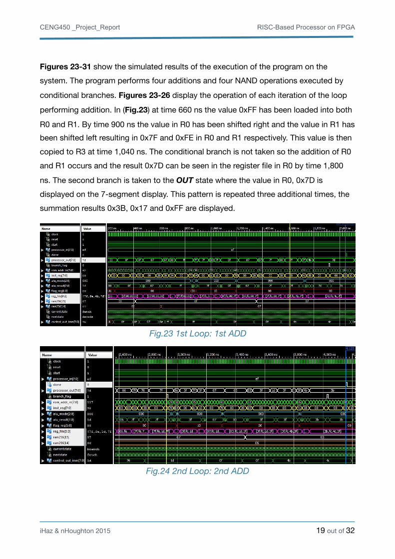
Figures 23-31 show the simulated results of the execution of the program on the system. The program performs four additions and four NAND operations executed by
conditional branches. Figures 23-26 display the operation of each iteration of the loop
performing addition. In (Fig.23) at time 660 ns the value 0xFF has been loaded into both
R0 and R1. By time 900 ns the value in R0 has been shifted right and the value in R1 has been shifted left resulting in 0x7F and 0xFE in R0 and R1 respectively. This value is then copied to R3 at time 1,040 ns. The conditional branch is not taken so the addition of R0 and R1 occurs and the result 0x7D can be seen in the register file in R0 by time 1,800
ns. The second branch is taken to the OUT state where the value in R0, 0x7D is displayed on the 7-segment display. This pattern is repeated three additional times, the summation results 0x3B, 0x17 and 0xFF are displayed.
� Fig.23 1st Loop: 1st ADD
� Fig.24 2nd Loop: 2nd ADD
�iHaz & nHoughton 2015 � out of �19 32
CENG450 _Project_Report RISC-Based Processor on FPGA�
� Fig.25 3rd Loop: 3rd ADD
� Fig.26 4th Loop: 4th ADD
The second portion of the program computes the NAND function. As can be seen in
(Fig.22) to execute the NAND the first conditional branch must be taken. In (Fig.27) at time 7,150 ns it can be seen that the branch flag is enabled signifying that the conditional branch was taken and the NAND operation was executed. For each NAND the expected result is 0xFF. It can be seen in figure 30 that at time 8,200 ns the value in the processor_out bus is 0xFF as expected and the done flag is enabled displaying the result on the 7-segment display. This process is repeated until program execution is
complete and can be viewed in figures 28-30.
�iHaz & nHoughton 2015 � out of �20 32
CENG450 _Project_Report RISC-Based Processor on FPGA�
� Fig.27 5th Loop: 1st NAND
� Fig.28 6th Loop: 2nd NAND
� Fig.29 7th Loop: 3rd NAND
�iHaz & nHoughton 2015 � out of �21 32
CENG450 _Project_Report RISC-Based Processor on FPGA�
� Fig.30 8th Loop: 4th NAND
(Fig.31) shows the final stage of the program, the unconditional branch to the start of the
program. At time 16,800 ns the branch flag is enabled and the program counter returns to instruction 2 as can be seen in the rom_addr_in bus (green).
� Fig.31 9th Loop: Start Again
�iHaz & nHoughton 2015 � out of �22 32
CENG450 _Project_Report RISC-Based Processor on FPGA�
ANALYSIS AND DISCUSSION
The combined functionality of the three instruction formats culminate to an effective RISC-like processor. The system is able perform computations, basic branching and memory management.
A-FORMAT
A-format instructions provide the unit’s basic functionality such as addition and
multiplication. (Fig.32) provides a visual example of this basic functionality. In the
simulation at time 1,005 ns the inputs to the ALU module are the hexadecimal values 0xC0 and 0x03. The ALU-mode value is ‘100’ which represents the function ‘ADD’ and the rf_write_index bus signals ‘10’ which signifies the destination register for the results is R3. The overall operation implements the summation of the hexadecimal values, the
result of which is stored in the register file in R3. In (Fig.8) at the completion of the write back stage at time 1,025 ns it can be seen in reg_file values (purple) that the expected result of 0xC3 has been successfully written into the third register file location. This basic demonstration proves the successful implementation of the A-format instructions. A provisional feature of the system A-format instructions is the intentional use of 2’s complement negative number computation in the ALU.
� Fig.32 A-Format Simulation Example ( 49: ADD r2, r1)
�iHaz & nHoughton 2015 � out of �23 32
CENG450 _Project_Report RISC-Based Processor on FPGA�
B-FORMAT
B-format instructions execute both conditional and unconditional branch operations in; figures 11 and 12 demonstrate the action taken. In (Fig.32) at time 9,955 ns the system
has received and approved a branch statement and the controller enables the branch_flag. The rom_addr_in bus increments sequentially until the branch flag is activated. At the completion of the currently executing instruction the branch target is loaded into the program counter from the register file enacting the branch mechanism.
As can be seen in (Fig.11) the branch function completes successfully.
� Fig.32 B-Format Simulation Example ( 96: BR r2)
L-FORMAT
The L-format instructions provide the system the ability to send and retrieve information
between the computational core and the small local RAM. (Fig.33) provides an example of a successful load operation from the RAM. The L-format instruction works in two stages. At time 275 ns instruction number 4, containing the first portion of the LOADIMM command, is loaded into the instruction register. Upon receipt of a LOADIMM in the instruction register the controller knows that the subsequent instruction will be the immediate value to be loaded or stored. When it arrives it is stored in the IMR register. At time 295 ns the immediate value is received by the controller which then activates the imr2_sel line (grey) beginning the load process. The immediate value in the IMR register is loaded onto the control_out_imm bus (orange) and the rf_write_index bus (purple) is given the target register value. At time 325 ns it can be seen that the value 0x0C has been successfully loaded into register R1 in (RF).�iHaz & nHoughton 2015 � out of �24 32
CENG450 _Project_Report RISC-Based Processor on FPGA�
�
Fig.33 L-Format Simulation Example ( 34,0C: LOADIMM r1, 0C)
PROCESSOR I/O AND HARDWARE IMPLEMENTATION
The processor implementation described above was successfully implemented on a Xilinx Spartan 3E FPGA installed on a Nexys2 circuit board. The Nexys2 board contains a four-digit common anode seven-segment LED display. To simplify the execution verification the processor_out bus of the processor was connected to two of the seven-segment displays. Two active-high push buttons were used for input control, one as a system reset and one as a program continue. A ‘stop and wait’ procedure was implemented in the processor, activated when the controller reaches the ‘out’ state. Referring to (Fig.22) when test program 2 completes a computation and displays the
result on the 7-segment displays via the controller’s ‘out’ state the controller halts system execution and waits for activation of the ‘continue’ push-button; upon the activation of which the program execution continues normally. This continue feature allows the clock to be set at any frequency while maintaining the ability to verify program execution.
�iHaz & nHoughton 2015 � out of �25 32
CENG450 _Project_Report RISC-Based Processor on FPGA�
For demonstration purposes the external system clock was set to 200 Hz (>150) allowing rapid program execution and verification, especially for the 7-segment to display the two digits at the same time. We also added the Display controller VHDL file to the project in order to display the output on the 7-segments in Digilent Nexys2 Board. The following settings were used:
● clk is external clock FPGA pin U9, reset and start are FPGA pin B18 and pin H13● hex3, hex2,hex1 and hex0 are four bit arrays used to store hex display character.
We used only hex1 and hex0 as we have only two digits● an (an0,an1, an2, an3) four bit array that connect to the display transistors● sseg 7bit array that stores the individual segments of the hex display
� Fig.34 Test Program 2 running on Spartan FPGA
�iHaz & nHoughton 2015 � out of �26 32
CENG450 _Project_Report RISC-Based Processor on FPGA�
CONCLUSION
A pipelined processor employing RISC-like instructions was implemented on a Xilinx Spartan 3E FPGA installed on a Nexys2 circuit board. The design was verified via the execution of two test programs designed to use and stress every instruction in the system. The design includes a 1-byte register file, a 256 byte ROM and 256 byte RAM, dynamic controller and support modules. The system successfully employs multiple arithmetic instructions, two conditional and one unconditional branch instruction as well as memory management instructions. Verification programs were executed on the Spartan FPGA and verified using two 7-segment displays and two push button inputs and an system frequency of 150 Hz.
�iHaz & nHoughton 2015 � out of �27 32
CENG450 _Project_Report RISC-Based Processor on FPGA�
APPENDIX (TABLES)
FSM CONTROL STATES (VHDL)
Table 1: FSM Control States
All outputs are Initialized WHEN ALU =>
WHEN S0 => Flag_Reg <={Z,N};
IF (Start = '1') THEN ALU-Mode <=Inst_reg(6-4)
PC_en <= ‘1’; Except for NAND
NextState <= Fetch; IN_Sel <= ‘0’;
Else IMR2_Sel <= ‘0’;
NextState <= S0; “ST”: IMR2_Sel, RAM_WR
End If; “LD,LDIm”: IMR2_Sel
WHEN Fetch => “IN”: IN_Sel, IMR2_Sel
All outputs are ‘0’ NextState <= Write_Back;
Inst_reg <= ROM_out; WHEN Branch =>
NextState <= Decode; ALU-Mode <= “000”;
WHEN Decode => PC_en <= ‘1’;
“Check (Inst_reg(7-4))” “Check (Inst_reg(3-2))”
A-Format (Arithmetic) “00/11”: Br_Sel
IN_Sel <= ‘1’; “01/10”: Br_Sel(Flag)
NextState <= ALU; NextState <= Fetch;
B-Format (Branch) WHEN Write_Back=>
NextState <= Branch; PC_en <= ‘1’;
“Return”: PC_en, Rt_Sel “Check (Inst_reg(7-4))”
NextState <= Fetch; “0/2/C”: RF_en <= ‘0’
A-Format (Arithmetic) “Others”: RF_en
PC_en <= ‘1’; “0001”: WB_Sel
NextState <= LD_ST; NextState <= Fetch;
�iHaz & nHoughton 2015 � out of �28 32
CENG450 _Project_Report RISC-Based Processor on FPGA�