Page 1
Design of the Configuration and Readout Electronics for a Multi-Channel IntegratedCircuit Used in the Detection and Monitoring of Ionizing Radiation
by SaiGeetha Allipuram, Bachelor of Science
A Thesis Submitted in PartialFulfillment of the Requirements
for the Degree ofMaster of Science
in the field of Electrical Engineering
Advisory Committee:
George L. Engel, Ph.D, Chair
Bradley Noble, D.Sc
Timothy York, Ph.D
Graduate SchoolSouthern Illinois University Edwardsville
May, 2019
Page 2
c© Copyright by SaiGeetha Allipuram May, 2019All rights reserved
Page 3
ABSTRACT
DESIGN OF THE CONFIGURATION AND READOUT ELECTRONICS FOR AMULTI-CHANNEL INTEGRATED CIRCUIT USED IN THE DETECTION AND
MONITORING OF IONIZING RADIATION
by
SAIGEETHA ALLIPURAM
Chairperson: Professor George L. Engel, Ph.D
This thesis describes the design of the configuration and readout electronics for a
multi-channel integrated circuit (IC) which is used in the detection and monitoring
of ionizing radiation in low- and intermediate-energy nuclear physics experiments.
The sixteen channel chip discussed in this thesis can be used in a wide variety of
nuclear physics applications and is suitable for use whenever silicon strip detectors
are employed.
The chip can be used to determine the energy of a charged particle striking the
detector, as well as, the the time interval between the arrival of the particle at the
detector and an externally supplied time reference. The configuration and readout
circuits, common to all of the sixteen signal processing channels, as well as the digital
logic contained within a single signal processing channel, was implemented using the
Verilog Hardware Description Language (HDL) and a 0.35 µm standard cell library.
Moreover, the IC christened HINP5 (Heavy Ion Nuclear Physics chip - Version 5), will
be fabricated using the AMS (Austrian Microsystems) 0.35 µm CMOS process in the
Fall of 2019.
ii
Page 4
The IC is configured via three 8-bit configuration registers. Moreover, each channel
contains a 6-bit Digital-to-Analog Converter (DAC) which must be programmed to set
a threshold used by the Constant Fraction Discriminator (CFD), located in the timing
branch within each channel. The IC supports data sparsification where a channel
automatically resets itself (after a programmable delay time) unless explicitly directed
to enter readout mode by an externally generated control signal.
The Verilog-driven design described in this thesis was implemented using Cadence’s
EDI (Encounter Digital Implementation) tools for synthesis and place n’ route. The
standard cell designs were then imported into Cadence’s Virtuoso custom IC tools
and validated at the electrical level. The use of the a standard cell approach greatly
reduced design time and allows for changes to be made easily to the readout and
configuration logic.
iii
Page 5
ACKNOWLEDGEMENTS
I would like to convey my sincere gratitude to Professor Dr. George Engel for
mentoring me in every phase of my Master’s study. His guidance helped me when I
was struggling during my research and also during the writing of this thesis. I could
not have envisioned a better mentor for my Master’s work. I also wish to thank Dr.
Lee Sobotka, Mr. Jon Elson, and Dr. Robert Charity (Department of Chemistry at
Washington University Saint Louis) for their constant support in this project. I would
like to thank my fellow graduate students: Bryan Orabutt, Lakshmi Teja Vipparla,
Jayasurya Burla, Anil Korkmaz, Monjour Rafi, Lohith Chowdary Chilukuri and all of
the others who contributed to the design of the HINP5 chip.
I wish to thank the National Science Foundation (NSF) for supporting my research
through NSF-MRI Grant # 1625499. I would also like to thank Dr. Timothy York,
Dr. Bradley Noble, Dr. Robert Leander, and the ECE faculty members at SIUE, who
have supported me throughout my education at SIUE. With their support, I was able
to explore new horizons.
I would not have achieved my goals without my companions Dheeraj, Vaibav,
Lavanya, Sindhu, and Sohan who have supported me during my graduate studies.
Finally, I would like to extend my appreciation to my family: my father Venkat Reddy
Allipuram, mother, sister and brother are always with me in every aspect.
iv
Page 6
TABLE OF CONTENTS
ABSTRACT . . . . . . . . . . . . . . . . . . . . . . . . . . . . . . . . . . . . ii
ACKNOWLEDGEMENTS . . . . . . . . . . . . . . . . . . . . . . . . . . . . iv
LIST OF FIGURES . . . . . . . . . . . . . . . . . . . . . . . . . . . . . . . . viii
LIST OF TABLES . . . . . . . . . . . . . . . . . . . . . . . . . . . . . . . . . ix
Chapter
1. INTRODUCTION . . . . . . . . . . . . . . . . . . . . . . . . . . . . 1
1.1 Research Background . . . . . . . . . . . . . . . . . . . . . . . . 11.2 HINP IC . . . . . . . . . . . . . . . . . . . . . . . . . . . . . . . 3
1.2.1 Linear circuits . . . . . . . . . . . . . . . . . . . . . . 41.2.2 Timing circuits . . . . . . . . . . . . . . . . . . . . . 61.2.3 Configuration and readout circuits . . . . . . . . . . 6
1.3 Previous Work . . . . . . . . . . . . . . . . . . . . . . . . . . . . 71.4 Object and Scope of Work . . . . . . . . . . . . . . . . . . . . . 8
2. SYSTEM LEVEL DESIGN . . . . . . . . . . . . . . . . . . . . . . . 10
2.1 Introduction . . . . . . . . . . . . . . . . . . . . . . . . . . . . . 102.2 System Operation . . . . . . . . . . . . . . . . . . . . . . . . . . 102.3 MotherBoard . . . . . . . . . . . . . . . . . . . . . . . . . . . . . 132.4 Chipboard FPGA . . . . . . . . . . . . . . . . . . . . . . . . . . 152.5 PicoBlaze Soft Core . . . . . . . . . . . . . . . . . . . . . . . . . 162.6 HINP Interface . . . . . . . . . . . . . . . . . . . . . . . . . . . . 202.7 Analog-to-Digital Converter . . . . . . . . . . . . . . . . . . . . . 21
3. COMMON CHANNEL . . . . . . . . . . . . . . . . . . . . . . . . . . 24
3.1 Digital Design Using EDI Tools . . . . . . . . . . . . . . . . . . . 253.1.1 Why Standard Cell Design . . . . . . . . . . . . . . . 253.1.2 Standard Cell Design Flow . . . . . . . . . . . . . . . 26
3.2 Configuration and Readout Electronics . . . . . . . . . . . . . . 313.2.1 Address Register . . . . . . . . . . . . . . . . . . . . 313.2.2 Configuration Registers . . . . . . . . . . . . . . . . 333.2.3 Mode Decoding Circuitry . . . . . . . . . . . . . . . 373.2.4 Shadow Register . . . . . . . . . . . . . . . . . . . . 413.2.5 OR Generation . . . . . . . . . . . . . . . . . . . . . 42
v
Page 7
3.2.6 Channel Address Generation Circuitry . . . . . . . . 433.2.7 Channel Select Generation Circuitry . . . . . . . . . 453.2.8 4-to-16 Decoder . . . . . . . . . . . . . . . . . . . . . 46
4. SIGNAL CHANNEL . . . . . . . . . . . . . . . . . . . . . . . . . . . 47
4.1 Hit Register . . . . . . . . . . . . . . . . . . . . . . . . . . . . . 474.2 Auto Reset Generation . . . . . . . . . . . . . . . . . . . . . . . 494.3 Analog Reset Generation . . . . . . . . . . . . . . . . . . . . . . 494.4 DAC . . . . . . . . . . . . . . . . . . . . . . . . . . . . . . . . . 50
5. SUMMARY. CONCLUSIONS, AND FUTURE WORK . . . . . . . . 55
5.1 Summary . . . . . . . . . . . . . . . . . . . . . . . . . . . . . . . 555.2 Conclusions . . . . . . . . . . . . . . . . . . . . . . . . . . . . . . 555.3 Future Work . . . . . . . . . . . . . . . . . . . . . . . . . . . . . 57
REFERENCES . . . . . . . . . . . . . . . . . . . . . . . . . . . . . . . . . . . 61
APPENDICES . . . . . . . . . . . . . . . . . . . . . . . . . . . . . . . . . . . 63
A. Verilog Description of Digital Design Implemented in HINP5 . . . . . 63
A.1 Verilog description of the digital circuits in common channel . . . 63A.1.1 Verilog description of shadow register . . . . . . . . . 66
A.2 Verilog description of the digital circuits in a signal channel . . . 67A.3 Verilog description of HINP channels . . . . . . . . . . . . . . . . 68
B. System Verilog Test Fixture for Verification . . . . . . . . . . . . . . 71
B.1 SystemVerilog definition of global parameters . . . . . . . . . . . 71B.2 SystemVerilog tasks . . . . . . . . . . . . . . . . . . . . . . . . . 72B.3 SystemVerilog test bench for verification . . . . . . . . . . . . . . 78
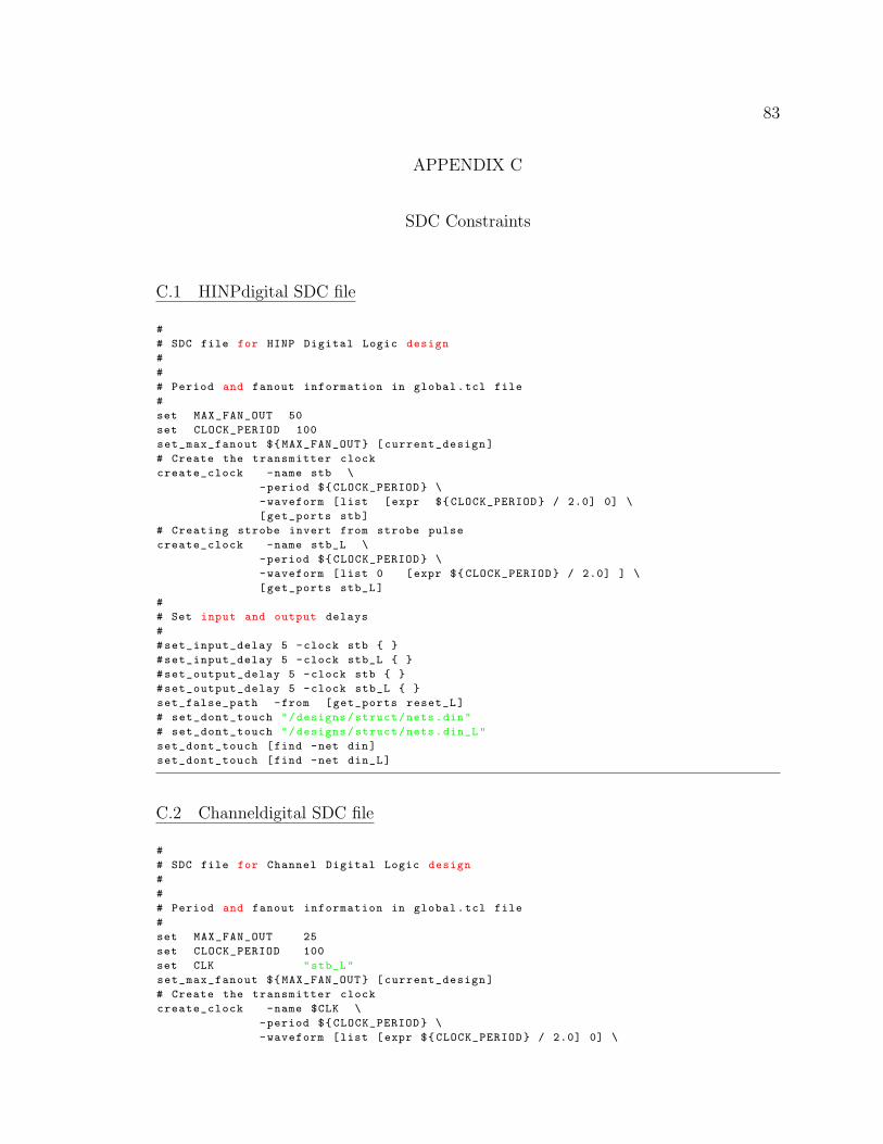
C. SDC Constraints . . . . . . . . . . . . . . . . . . . . . . . . . . . . . 83
C.1 HINPdigital SDC file . . . . . . . . . . . . . . . . . . . . . . . . 83C.2 Channeldigital SDC file . . . . . . . . . . . . . . . . . . . . . . . 83
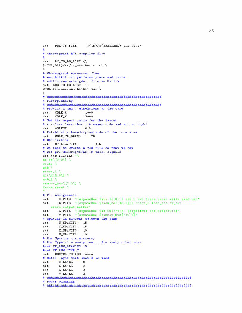
D. Environment Files Used in Design . . . . . . . . . . . . . . . . . . . . 85
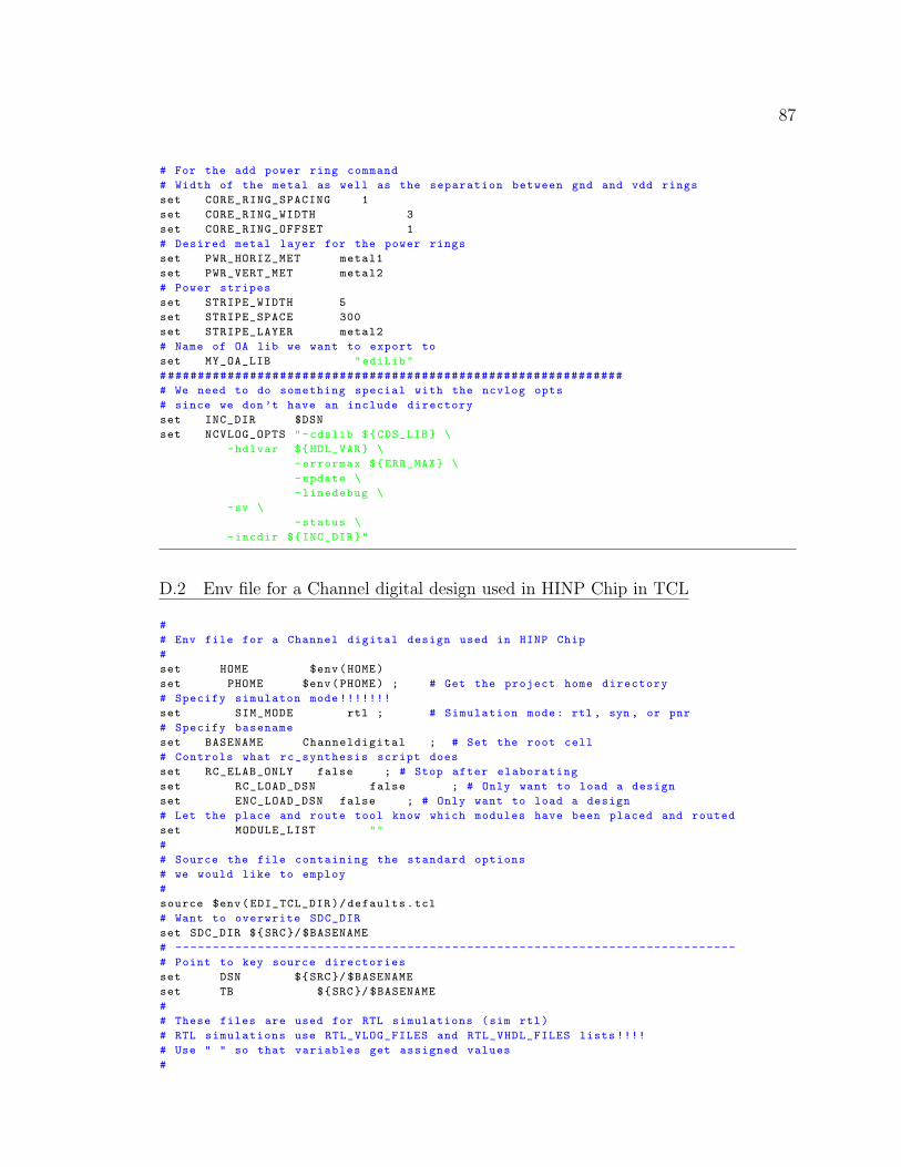
D.1 Env file for a HINP digital design used in HINP Chip in TCL . . 85D.2 Env file for a Channel digital design used in HINP Chip in TCL 87
vi
Page 8
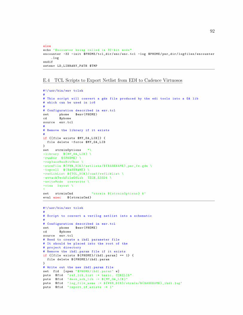
E. TCL Scripts for EDI . . . . . . . . . . . . . . . . . . . . . . . . . . . 90
E.1 TCL Script to run Simulation . . . . . . . . . . . . . . . . . . . . 90E.2 TCL Script to run Synthesis . . . . . . . . . . . . . . . . . . . . 91E.3 TCL Script to run Place n’ Route . . . . . . . . . . . . . . . . . 91E.4 TCL Scripts to Export Netlist from EDI to Cadence Virtuosos . 92
F. Scripts to Generate Piece Wise Linear files from the VCD Dump file . 94
F.1 Make VCD TCL Script . . . . . . . . . . . . . . . . . . . . . . . 94F.2 VCD to PWL python script . . . . . . . . . . . . . . . . . . . . . 97
vii
Page 9
LIST OF FIGURES
Figure Page
1.1 An array of si strip detectors . . . . . . . . . . . . . . . . . . . . . . 21.2 Block diagram of typical HINP5 channel[Korkmaz, 2019]. . . . . . . . 5
2.1 Block Diagram of the System . . . . . . . . . . . . . . . . . . . . . . 122.2 Block Diagram of the MotherBoard . . . . . . . . . . . . . . . . . . . 132.3 Chipboard connected to one of the 16 slots on motherboard . . . . . 142.4 Spartan 3AN Architecture . . . . . . . . . . . . . . . . . . . . . . . . 162.5 PicoBlaze Embedded Microcontroller . . . . . . . . . . . . . . . . . . 182.6 PicoBlaze top-level Interface Connections . . . . . . . . . . . . . . . . 192.7 Channel Selection Bits in LTC1865 . . . . . . . . . . . . . . . . . . . 222.8 Operating Sequence Diagram . . . . . . . . . . . . . . . . . . . . . . 23
3.1 An example of a VCD file . . . . . . . . . . . . . . . . . . . . . . . . 303.2 Generic schematic of logic that resides in the common channel . . . . 323.3 Mode Decoding Logic implementation in common channel . . . . . . 373.4 Shadow Register . . . . . . . . . . . . . . . . . . . . . . . . . . . . . 423.5 Circuit that generates OR OUT signal . . . . . . . . . . . . . . . . . 433.6 Channel Address Generation Circuit . . . . . . . . . . . . . . . . . . 433.7 Channel Select Generation Circuit . . . . . . . . . . . . . . . . . . . 45
4.1 Hit Register . . . . . . . . . . . . . . . . . . . . . . . . . . . . . . . . 484.2 Auto Reset Generation Circuitry . . . . . . . . . . . . . . . . . . . . 494.3 Analog Reset Generation Circuitry . . . . . . . . . . . . . . . . . . . 504.4 DAC Register . . . . . . . . . . . . . . . . . . . . . . . . . . . . . . . 524.5 Generic schematic of the digital logic in the HINP5 signal channel . . 54
5.1 Layout of the HINP common channel digital logic generated bythe place n route tool . . . . . . . . . . . . . . . . . . . . . . . . . 58
5.2 Layout of the HINP signal channel digital logic generated by theplace n route tool . . . . . . . . . . . . . . . . . . . . . . . . . . . 59
viii
Page 10
LIST OF TABLES
Table Page
3.1 Bit assignments of configuration register 0 . . . . . . . . . . . . . . . 343.2 Bit assignments of configuration register 1 . . . . . . . . . . . . . . . 353.3 Bit assignments of configuration register 2 . . . . . . . . . . . . . . . 363.4 Modes of Operation . . . . . . . . . . . . . . . . . . . . . . . . . . . 393.5 Modes of Operation Continued . . . . . . . . . . . . . . . . . . . . . 403.6 Truth Table of Priority Encoder . . . . . . . . . . . . . . . . . . . . . 44
4.1 Bit assignments of DAC register in signal channel . . . . . . . . . . . 53
ix
Page 11
CHAPTER 1
INTRODUCTION
This chapter is intended to introduce the reader to the subject of radiation monitoring
and will describe how custom multi-channel integrated circuits are useful in the
detection and measurement of ionizing radiation. The IC (Integrated Circuit) outlined
in this thesis, called HINP5 (Heavy-Ion Nuclear Physics- Version 5), is the newest
chip in our research group’s CMOS (Complementary Metal-Oxide Semiconductor)
ASIC (Application Specific Integrated Circuit) ”tool box” for radiation detection. The
ICs in the ”tool box” are being developed by the IC Design Research Laboratory at
Southern Illinois University Edwardsville (SIUE) in alliance with researchers from the
Nuclear Reactions Group at Washington University in Saint Louis (WUSTL).
1.1 Research Background
The IC Design Research Laboratory at SIUE in collaboration with the Nuclear
Reactions Group (Department of Chemistry) at WUSTL have been working, since
2001, to develop a class of multi-channel custom integrated circuits (ICs) useful for
researchers engaged in various nuclear physics experiments where the identification
and measurement of ionizing radiation is required. Usually in these experiments, the
position of interaction within the detector must be precisely estimated, the particle
energy must be measured, and the relative time of arrival of the particle must be
determined.
The groups first achievement was an analog shaped and peak sensing chip. It had
on-board CFD (Constant-fraction Discriminators) and sparsified readout. It is known
as HINP (Heavy-Ion Nuclear Physics). The chip was designed for use with Si-strip
detectors. The second chip, called PSD (Pulse Shape Discrimination), was designed
Page 12
2
to complement the HINP chip logically in terms of being able to support different
detector types. PSD8C is used with scintillators and uses almost the same supporting
hardware as does HINP. This thesis is devoted to describing the digital logic contained
within the latest generation HINP chip known as HINP5 (HINP Version 5). A typical
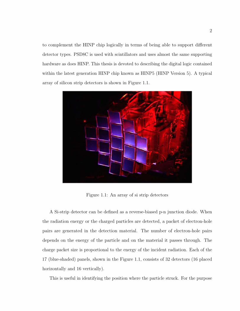
array of silicon strip detectors is shown in Figure 1.1.
Figure 1.1: An array of si strip detectors
A Si-strip detector can be defined as a reverse-biased p-n junction diode. When
the radiation energy or the charged particles are detected, a packet of electron-hole
pairs are generated in the detection material. The number of electron-hole pairs
depends on the energy of the particle and on the material it passes through. The
charge packet size is proportional to the energy of the incident radiation. Each of the
17 (blue-shaded) panels, shown in the Figure 1.1, consists of 32 detectors (16 placed
horizontally and 16 vertically).
This is useful in identifying the position where the particle struck. For the purpose
Page 13
3
of identifying position, two silicon detectors of differing thickness are used (65 µm
and 1.5 mm). The 65 µm detector is single-sided with silicon strips in the vertical
direction while the 1.5 mm detector is double-sided with silicon strips that are vertical
in the front and horizontal on the back.
1.2 HINP IC
As already discussed, HINP5 stands for Heavy Ion Nuclear Physics - Version 5
and is a 16-channel chip. HINP5 is a multi-channel chip which generates sparsified
analog pulse trains for both timing information (in respect to an external reference)
and for linear (pulse height) information. HINP5 is the latest version of the earlier
HINP chips. HINP5 is a custom intergrated circuit that posses some special features
which no commercial IC possesses. Special features of HINP5 are:
• Sixteen(16) independent channels
• Has two different modes operating in parallel: low-gain mode (400 Mev full-range)
and high-gain mode(100 Mev full-range)
• Fast analog multiplicity and channel OR output to help in making decisions
about whether to readout or not
• Auto-reset capability allows for data sparsification
• Supports both negative and positive polarity pulses
• Built-in time-to-voltage converters supporting 250 nsec and 2 µsec full-scale
ranges
• Has on-chip CFDs (Constant Fraction Discriminators)
• Better noise performance(<25 keV)
Page 14
4
• Can also be used with external charge amplifier
The architecture of a single HINP5 channel is shown in Figure 1.2. Each of the
HINP channels consists of the following primary blocks: charge amplifier (CA), a
pair of slow shapers, a pseudo-constant fraction discriminator (CFD), a pair of peak
samplers, and a time-to-voltage converter (TVC). The signal channels also contains
some bias circuits, reset logic, and digital readout electronics.
The HINP5 chip is designed using the AMS 0.35 µm CMOS process. This CMOS
process supports 4 metal (Metal 4 is an extra thich metal layer) and 2 polysilicon
layers. Designers using this process have access to both 5 V (PMOSM, NMOSM) and
3.3 V (PMOS, NMOS) FETs, Bipolar Junction Transistors (BJTs), and two kinds of
resistors implemented using the POLY 2 layer. One is RPOLYH (lightly doped POLY
2 layer) and the other is RPOLY2 (heavily doped POLY 2 layer). The designer also
has access to double poly capacitors (CPOLY). In the design described in this thesis,
3.3 V FETs (PMOS,NMOS) are used which are faster (and smaller) than the 5 V
FETs. The minimum length of the 3.3 V FETs is 0.35 µm.
As shown in Figure 1.2, HINP5 consists of three major blocks: linear circuits,
timing circuits, and the configuration/readout circuits. In the next section we will
briefly describe operation of a HINP5 signal processing channel.
1.2.1 Linear circuits
The first element in the linear block is the charge amplifier (CA) and it is designed
to have two outputs: high-gain (charge gain of x4) and low-gain (charge gain of x1).
Additionally, one can also utilize an external preamplifier. The purpose of the CA is
to amplify the input charge packet either by a gain of 1 (low-gain) or by a gain of 4
(high-gain).
Page 15
5
Figure 1.2: Block diagram of typical HINP5 channel[Korkmaz, 2019].
The two outputs (currents) from the CA are the inputs to a pair of slow shapers
(Gaussian low-pass filters). The low-gain shaper output is linear to 400 MeV while
the high-gain shaper output is linear to 100 MeV. Each of these sub-channels generate
sparsified analog pulse trains along with synchronized addresses for digitization by an
off-chip analog-to-digital converter (ADC) [Sadasivam, 2002].
Since it is the peak voltage at the output of the pulse shaper which is proportional
to the detected particle energy, the outputs from the two shapers are presented to a
pair of peak-samplers before being sent off-chip to be digitized by the ADCs. The
input to the slow shaper is a charge packet. The peak sampler was designed to find
only negative peaks, so depending on the polarity (i.e. electron or hole collection) the
output from the shaper may be inverted prior to peak detection.
Page 16
6
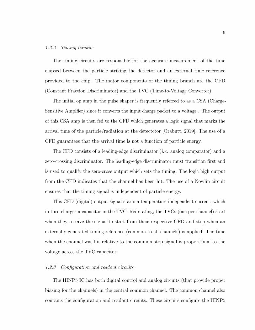
1.2.2 Timing circuits
The timing circuits are responsible for the accurate measurement of the time
elapsed between the particle striking the detector and an external time reference
provided to the chip. The major components of the timing branch are the CFD
(Constant Fraction Discriminator) and the TVC (Time-to-Voltage Converter).
The initial op amp in the pulse shaper is frequently referred to as a CSA (Charge-
Sensitive Amplfier) since it converts the input charge packet to a voltage . The output
of this CSA amp is then fed to the CFD which generates a logic signal that marks the
arrival time of the particle/radiation at the detectctor [Orabutt, 2019]. The use of a
CFD guarantees that the arrival time is not a function of particle energy.
The CFD consists of a leading-edge discriminator (i.e. analog comparator) and a
zero-crossing discriminator. The leading-edge discriminator must transition first and
is used to qualify the zero-cross output which sets the timing. The logic high output
from the CFD indicates that the channel has been hit. The use of a Nowlin circuit
ensures that the timing signal is independent of particle energy.
This CFD (digital) output signal starts a temperature-independent current, which
in turn charges a capacitor in the TVC. Reiterating, the TVCs (one per channel) start
when they receive the signal to start from their respective CFD and stop when an
externally generated timing reference (common to all channels) is applied. The time
when the channel was hit relative to the common stop signal is proportional to the
voltage across the TVC capacitor.
1.2.3 Configuration and readout circuits
The HINP5 IC has both digital control and analog circuits (that provide proper
biasing for the channels) in the central common channel. The common channel also
contains the configuration and readout circuits. These circuits configure the HINP5
Page 17
7
chip. The readout circuits provide data in the form of three analog pulse trains
(high-gain peak voltage, low-gain peak voltage, and the TVC voltage) along with
synchronized digitally encoded channel addresses to the off-chip ADCs and FPGA
(Field Programmable Gate Array) logic.
As shown in the Figure 1.2, the configuration circuitry consists of three 8-bit
registers that can be loaded selectively to generate various control signals. The control
signals generated by the configuration registers are capable of setting the Nowlin delay,
setting Nowlin mode (short versus long), adjusting the AGND (signal ground) voltage,
selecting even channels or odd channels for pulsing, and selecting TVC measurement
range. The TVC can be switched between the two ranges: 250 ns full-scale and 2 µs
full-scale. The biasing, configuration, and the readout circuits are positioned at the
center of the chip.
1.3 Previous Work
The fundamental architecture of the HINP chip has remained relatively unaltered
over the span of many design revisions until recently being significantly changed.
The first HINP IC designed had 16 signal channels. It was called HINP16C and
unfortunately was never used in experiments due to a design error. It had design issues
such as poor linearity and poor noise performance. The revised HINP IC, HINP2, with
16 channels was used in many experiments using the HiRA (High Resolution Array)
Si array had two internal CSA (Charge Sensitive Amplifier) gain modes. The modes
were referred to as high-gain (dynamic range of 400 MeV) and low-gain (dynamic
range of 100 MeV). The gain modes could not, however, be used at the same time. It
had a shaper with a fixed peaking time of 1.2 µs , and each channel possessed a TVC
with two time ranges: 250 ns and 2 µs.
HINP3 (version 3) had a few additional features such as a shadow register, and the
Page 18
8
fast shaper circuit in the CFD module was modified to make it programmable. The
addition of the shadow register helps users to determine which channels have been hit
prior to readout whereas the modification of the fast shaper circuit allows users to select
one of two time constants. The HINP3 IC displayed considerably better performance
in terms of both linearity and energy resolution i.e. the internal CSA gains were 30%
greater compared to the HINP2 design. The timing performance of HINP3 was also
proven to be better along with the additional features. But unfortunately the changes
made to integrate the shadow register into the design affected the auto-reset circuit
which makes the data sparsification feature of the chip possible.
Later, HINP4 (version 4) was fabricated to correct the problem with the auto-reset
circuit, increase the dynamic range properties and also to remedy some of the issues
identified with the on-chip TVC circuits. In HINP4, even though some of the channels
displayed good linearity, some (random from chip to chip) of the other channels
suffered from linearity issues. The version 5 IC, detailed within this thesis, is designed
to achieve even better performance than its antecedents in terms of linearity and
noise. This thesis describes in detail the digital configuration and readout electronics
implemented in the HINP5 chip.
1.4 Object and Scope of Work
The object of this thesis work is to design the readout and configuration circuits
for HINP5. HINP5 is intended for use in the detection and measurement of ionizing
radiation in instruments used for experiments in low- and intermediate-energy nuclear
physics and for researchers working with radioactive ion beams. HINP5, like the
earlier versions, is an analog shaped and peak sensing chip used with arrays of Si-strip
detectors.
There are five chapters in this thesis. Chapter 1 has a brief introduction about the
Page 19
9
evolution and architecture of the HINP IC. In Chapter 2, we will describe the overall
system-level design. In particular, the chipboards upon which the HINP chips reside
along with the motherboard that the chipboarbs are plugged into will be discussed.
A discussion of how the HINP chip interfaces to the chipboard FPGA. Chapter 3
describes in detail the digital circuits which reside in the common channel of HINP5. In
Chapter 4, the digital logic contained within an individual signal channel is described
in detail. Finally, Chapter 5 will provide a summary of the work done so far, and
describes the future work that needs to be done on HINP5.
This thesis focuses only on the design of the digital configuration and readout
electronics residing on HINP5. Details about the linear branch circuits in HINP5 are
covered in another thesis [Korkmaz, 2019], and the details on the timing branch of
HINP5 are discussed in yet a third thesis [Burla, 2019]. An earlier thesis describes
the CFD related circuits [Orabutt, 2019].
Page 20
10
CHAPTER 2
SYSTEM LEVEL DESIGN
2.1 Introduction
In this Chapter we will discuss the Field Programmable Gate Array(FPGA) and
its design which directly interfaces to the HINP5 ICs. Before going into details about
the FPGA design, there is a need to understand the system level design where the
FPGA interacts with a motherboard, two HINP chips and several ADCs. Bold-faced
words in this chapter correspond to signal names.
2.2 System Operation
The HINP5 chip generates analog pulse train outputs for both timing and energy
along with synchronized digitally encoded channel addresses. There is a need to
digitize the analog outputs using an external Analog to Digital Controller (ADC).The
reason for digitization is that transmitting high resolution analog data is prone to
degradation due to environmental noise where as transmitting the digital data is less
prone to loss when transmitted over significant distances.
The chipboards (CBs), which in turn plug into the motherboard (MB), are designed
so that the analog outputs from the HINP5 chip are digitized locally. The chipboard
contains two HINP5 ICs, a Spartan 3A Xilinx FPGA, three ADCs, and a small
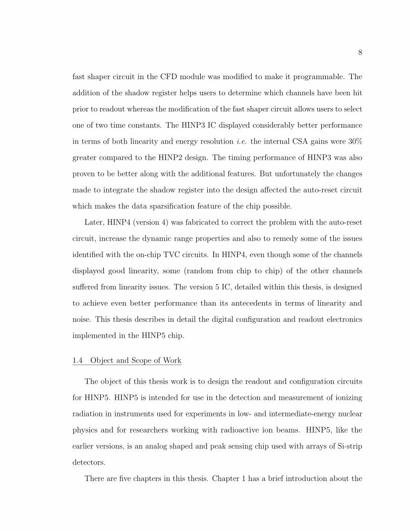
amount of support circuitry. The Xilinx Field Programmable Gate Array (FPGA),
shown in the Figure 2.1 supports two 8-bit PicoBlaze micro-controllers. The PicoBlaze
is a softcore provided by Xilinx and must be programmed in assembly language
but uses relatively little resources on a Spartan3A FPGA. The analog pulse trains
produced by the HINP chip are digitized by the LTC1865 ADC manufactured by
Linear Technologies.
Page 21
11
The FPGA interfaces with the ADCs via a 4-wire digital interface. The 4-wire
digital interface consists of SCLK (serial clock), SDI (serial data in), SDO (serial
data out) and CONV (start conversion). The analog data from both of the HINP
chips is simultaneously digitized and stored in the FPGA memory.
The Xilinx FPGA contains a two-port shared Random Access Memory (RAM).
The two PicoBlazes share the memory. The motherboard acquires data from the
FPGA by issuing four acquisition clocks per channel. On the first clock the chip ID
and channel address will be read out. On succeeding clock pulses the ADC data for
the A, B, and T values will be read out where A is the high gain pulse shaper output,
B is the low gain pulse shaper output. The digitized data(A, B, and T) stored in the
FPGA memory is sent to the motherboard and then transferred to the XLM.
Page 22
12
Figure 2.1: Block Diagram of the System
Page 23
13
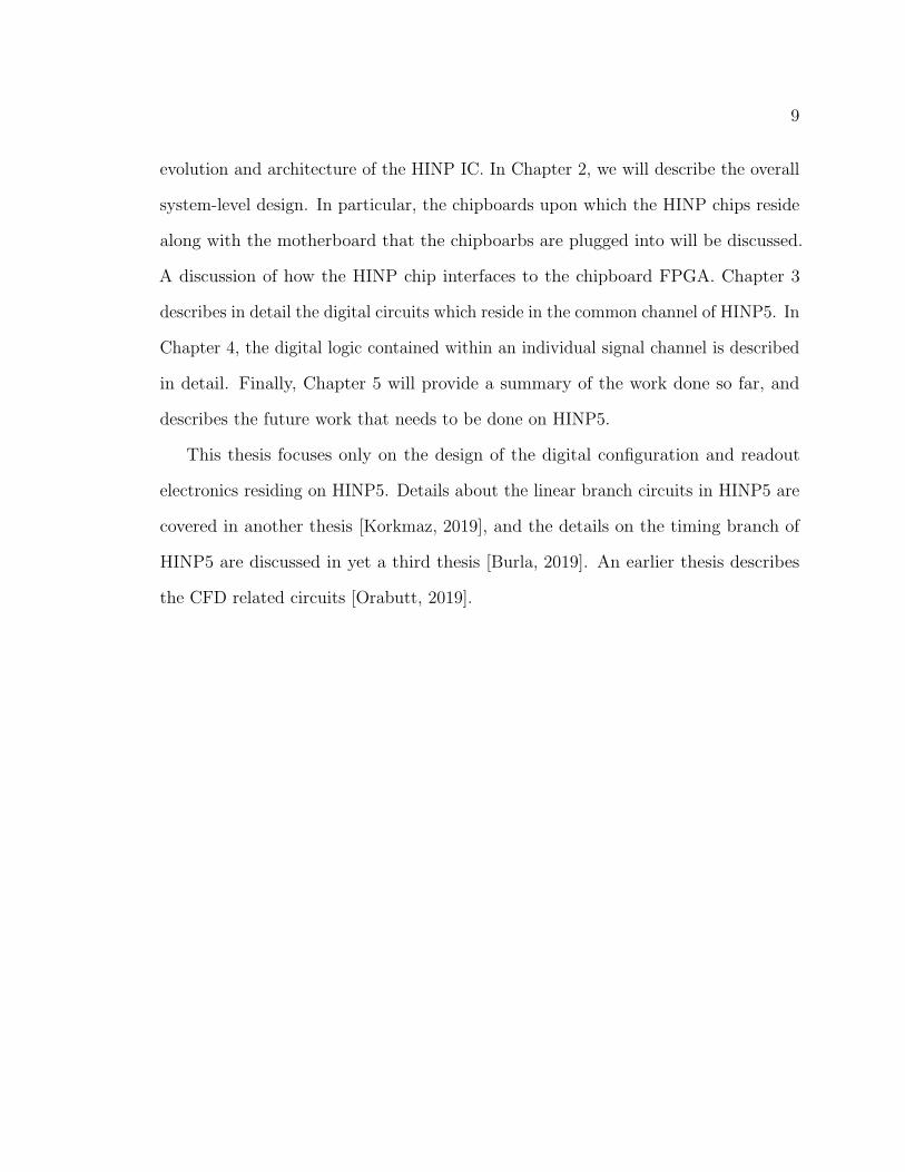
2.3 MotherBoard
The motherboard (MB) has sixteen slots. The CBs, briefly described in the
previous section, plug into these slots. Hence, a single MB can services 512 Si-strip
detectors. The power supply generation block on the MB is capable of generating 1.2
V, 3.3 V and 5 V. The supply voltages 1.2 V and 3.3 V are distributed to the HINP
CBs.
The multiplicity circuits on the MB recieve analog multiplicity outputs from the
sixteen slots. Multiplicity outputs are analog voltages proportional to the number of
channels which have been struck by radiation. Each HINP5 chip in the system produces
a multiplicity output. Everytime a channel is ”hit”, the multiplicity output goes up
by approximately 100 mV. If all sixteen channels on the HINP chip have been hit
then approximately 1.6 V is observed on the multiplicity output pin [Orabutt, 2019].
Figure 2.2: Block Diagram of the MotherBoard
The MB generates a master clock (STB) inside the motherboard FPGA and
Page 24
14
a master reset (RESET L). They are reproduced and used by the FPGA on the
chipboard. The TAKE EVENT, ACQ CLK, and ACQ ACK signals are used to
acquire ADC data. The global enable (GLOBAL ENA) signal enables the sixteen
channels of the HINP chip globally. If the bit is set (GL0BAL ENA = 1) then all
of the channels in the HINP chip are enabled. In addition, each channel has its own
channel register which enables/disables that particular channel. The channel OR
(OR OUT) and MULTIPLICITY signals are sent to the MB. These signals indicate
if any of the channels have yet to be read out. The reset signals : FORCE RESET
and RESET L signals are asserted from the motherboard. RESET L is a master
reset signal which is active low and FORCE RESET when active resets all the
signals. This is done usually after the data acquisition process has completed. In
Figure 2.3, a chipboard is plugged into one of the sixteen slots on the motherboard.
Figure 2.3: Chipboard connected to one of the 16 slots on motherboard
Page 25
15
2.4 Chipboard FPGA
As already discussed, two HINP chips along with an FPGA and some support
circuitry reside on the system chip boards (CBs). In this section, we will briefly
describe the FPGA which is used on the CB.
A FPGA (Field Programmable Gate Array) can be defined as a Integrated Circuit
(IC) which provides designers with programmable logic blocks and memory blocks
(on-chip storage, RAM, PROM) etc. We use a Xilinx Spartan-3AN FPGA in our
design.
The Spartan-3AN FPGA supports non-volatile RAM storage, which is capable of
storing the configuration data of the FPGA. A JTAG interface is used to program
configuration data into the FPGA. The Spartan-3AN is a very cost-effective non-
volatile FPGA solution. The other key features of the Spartan-3AN FPGA are
[DS5, 2014]:
• Parallel NOR Flash configuration
• SPI serial Flash configuration: uses either the Atmel DataFlash architectures or
STMicroelectronics
• Parallel NOR and SPI serial Flash PROMs supports MultiBoot FPGA configu-
ration
• Embedded 8 bit PicoBlaze controller & 32 bit MicroBlaze processor
• Memory interfaces (DDR supported)
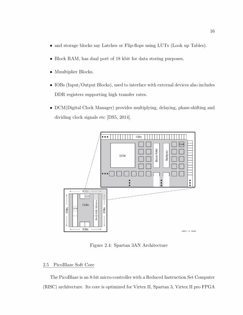
Figure 2.4 shows the 5 basic programmable logic elements of the Spartan-3AN
architecture.
• CLBs (Configurable Logic Blocks) that performs logic
Page 26
16
• and storage blocks say Latches or Flip-flops using LUTs (Look up Tables).
• Block RAM, has dual port of 18 kbit for data storing purposes,
• Muultiplier Blocks,
• IOBs (Input/Output Blocks), used to interface with external devices also includes
DDR registers supporting high transfer rates.
• DCM(Digital Clock Manager) provides multiplying, delaying, phase-shifting and
dividing clock signals etc [DS5, 2014].
Figure 2.4: Spartan 3AN Architecture
2.5 PicoBlaze Soft Core
The PicoBlaze is an 8-bit micro-controller with a Reduced Instruction Set Computer
(RISC) architecture. Its core is optimized for Virtex II, Spartan 3, Virtex II pro FPGA
Page 27
17
families [UG1, 2008]. It is completely embedded into the target FPGA and does not
require any external resources. It is extremely flexible and can interface to additional
FPGA logic via its I/O (Input/Output) ports. The PicoBlaze micro controller is
a good fit for this application, as it is compact and consumes less resources on the
FPGA when compared to other 8-bit micro-controllers available in the market. The
controller is programmed in assembly language. A PicoBlaze supports the following
features [UG1, 2008]:
• General purpose registers of 16 byte long for data
• 64 Byte internal scratchpad RAM (Random Access Memory)
• 1024 Instruction PROM (Programmable Read Only Memory)
• Can be expandable with 256X256 I/O ports
• 8 bit Arithmetic Logic Unit (ALU); provided Zero and Carry flags
• Automatic CALL/RETURN stack memory with 31 locations.
• Fast interrupt response
• Assembler with simulator that supports instruction set
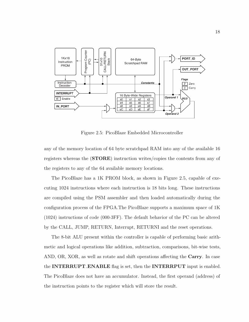
A block diagram of the PicoBlaze micro-controller is shown in Figure 2.5, It has
sixteen general purpose registers, designated as s0, s1, and so on through sF. All the
registers are similar with none of them reserved for special operations and has no
priorities set.
The PicoBlaze also has an internal 64 byte scratchpad RAM, addressable directly
(with immediate constants) or indirectly from the register file (using the register
contents) through FETCH and STORE commands. The FETCH instruction reads
Page 28
18
Figure 2.5: PicoBlaze Embedded Microcontroller
any of the memory location of 64 byte scratchpad RAM into any of the available 16
registers whereas the (STORE) instruction writes/copies the contents from any of
the registers to any of the 64 available memory locations.
The PicoBlaze has a 1K PROM block, as shown in Figure 2.5, capable of exe-
cuting 1024 instructions where each instruction is 18 bits long. These instructions
are compiled using the PSM assembler and then loaded automatically during the
configuration process of the FPGA.The PicoBlaze supports a maximum space of 1K
(1024) instructions of code (000-3FF). The default behavior of the PC can be altered
by the CALL, JUMP, RETURN, Interrupt, RETURNI and the reset operations.
The 8-bit ALU present within the controller is capable of performing basic arith-
metic and logical operations like addition, subtraction, comparisons, bit-wise tests,
AND, OR, XOR, as well as rotate and shift operations affecting the Carry. In case
the INTERRUPT ENABLE flag is set, then the INTERRPUT input is enabled.
The PicoBlaze does not have an accumulator. Instead, the first operand (address) of
the instruction points to the register which will store the result.
Page 29
19
The PicoBlaze has an automatic reset event. Once the FPGA configuration is
complete, it resets the value of the PC to address 0, disables the interrupts, clears
all the flags etc., but the scratchpad RAM and data registers are not affected by this
reset event. The PicoBlaze micro-controller is expandable as it supports 256 Input
and 256 Output ports. This allows the processor to interface to external peripheral
devices or other FPGA logic.
Figure 2.6: PicoBlaze top-level Interface Connections
Figure 2.6 shows the top-level interface signals of the PicoBlaze micro-controller:
• PORT ID (8-bit long) that outputs the port address,
• IN PORT (8-bit data line) that hold the data during an input operation where
data is read from this port to the specified register (sX) on the rising clock edge
if the READ STROBE is set,
• OUT PORT (8-bit data line) holds the data for 2 clock cycles during output
operations where the controller writes the data (contents of the register, sX) to
this port if WRITE STROBE is set,
• RESET (1-bit input) signal set to high for one clock cycle resets the PicoBlaze
controller automatically following the FPGA configuration,
Page 30
20
• CLK signal where all the PicoBlaze synchronous components are clocked with
rising clock pulses
• INTERRPUT ENABLE flag set then generates an
• INTERRUPT by setting this input for at-least 2 clock cycles, and if
• INTERRUPT ACK is set notifying that the INTERRPUT event happened
and the signal is set during the second clock cycle of the two-cycle interrupt.
2.6 HINP Interface
As discussed in the previous sections, each of the two PicoBlaze micro-controllers
in the FPGA are programmed to control one of the two HINP5 chips on the chipboard.
The PicoBlaze microcontrollers in the FPGA are programmed to configure both the
HINP5 chips and for acquisition of the analog pulse trains produced by the timing
and linear branches of HINP5. The HINP interface shown in Figure 2.1 consists of a
set of signals helpful in performing the various configuration and readout tasks.
The FPGA writes data into the address and configuration registers present inside
the common channel of the HINP5 chip. When the WRITE signal is made HIGH,
the address and mode information is loaded into the address register on the rising
edge of STB and configuration information is loaded into either the configuration
registers or the DAC registers on the falling edge based on the mode selected during
the rising edge. The data to be written is available on the 8-bit AD bus. AD is a
bidirectional bus which allows an user to input data into the HINP5 chip and output
data from the chip. The strobe, STB, is generated by the FPGA’s PicoBlaze.
During the readout process,the FPGA reads the address of the channel from the
HINP chip that is being processed, and it also monitors the OR OUT output from
Page 31
21
the HINP chip. The OR OUT is high when at least one channel on HINP has been
hit. After all channels have been read out the OR OUT will return to the low state.
Using the ACQ ALL signal, asserted from the motherboard, one can force the
acquisition of all the sixteen channels on chip. One can also select a particular channel
for data acquisition by giving the channel address on the bus externally when the
SEL EXT ADDR pin is asserted from the motherboard. The HINP chip receives
the COMMON STOP and GLOBAL ENA signals directly from the motherboard.
When the COMMON STOP is brought high, the TVC (Time to Voltage Converter)
in each of the sixteen channels will halt. GLOBAL ENA enables setting of the hit
registers. The readout electronics will be described in more detail in Chapter 3 and
Chapter 4.
2.7 Analog-to-Digital Converter
The chipboards use the Linear Technology’s LTC1865 Analog to Digital Converter
(ADC). It is a 16-bit Analog-to-Digital converter with a programmable 2 channel
MUX (Multiplexer, enabling it to operate in either the single-ended or differential
mode [ADC, ]. The conversion starts with the CONV signal going high and waits for
some time (t conv) to finish the conversion. After the conversion completes, the ADC
goes into sleep mode (just draws leakage current). A low on the CONV pin enables
the SDO pin and data is shifted out. The ADC converts analog data to digital and
that data is then transferred serially, synchronized to a clock, SCK. The SDI and the
SDO are the serial input and serial output data pins. Configuration bits are shifted
into the ADC and digital data is shifted out.
The ADC has two analog channels (CH0, CH1) The inputs to these channels
need to be noise-free respective to GND. The first two bits of the SDI input sequence
will configures the MUX as illustrated in the table below.
Page 32
22
Figure 2.7: Channel Selection Bits in LTC1865
As discussed above, the LTC1865 ADC starts conversion on the rising edge of the
CONV. When the CONV signal goes low, the 2-bit data is clocked into the SDI
pin on the rising edge of shift clock, SCK. Additional data bits clocked in on the
SDI pin are ignored until the next CONV cycle. The LTC1865 supports full-duplex
mode, where receiving and transmitting data is done simultaneously [ADC, ]. As
shown in Figure 2.8, the data transfer is synchronized with SCK where each bit is
transmitted on the falling edge of SCK and recieved on the rising edge of SCK in
both receiving and transmitting systems. After the completion of the data transfer,
if one continues to apply clock pulses with the CONV signal low, then the SDO
outputs zeros endlessly.
Page 33
23
Figure 2.8: Operating Sequence Diagram
Page 34
24
CHAPTER 3
COMMON CHANNEL
The HINP5 IC is made up of sixteen signal processing channels and a single common
channel placed in the center of the chip. The common channel in HINP5 contains
the digital configuration and readout logic as well as the analog bias circuits that are
common to all sixteen signal channels. The common channel contains analog circuits
such as the ”Power on Reset” (POR) circuit which generates an active low reset pulse
which is guaranteed to be at least 2 µsec long when HINP5 is first powered up. This
POR signal is used to start a PTAT (Proportional-to-Absolute-Temperature) current
generator which provides a 11.5 µA bias current to each of the 16 signal channels
[Orabutt, 2019].
An analog ”signal ground” generator circuit provides an analog signal ground
(AGND). AGND is generally set at a potential halfway between the AVDD and AVSS
rails. This signal ground is used in the analog circuitry in the signal channels as
well as by the off-chip single-to-differential buffers located in the common channel.
The nominal AGND reference voltage is around 1.65 V and can be trimmed using 3
configuration bits.
Each signal channel contains an auto-reset circuit which produces a reset signal
after a programmable delay defined by 4 configuration bits. The configuration bits
are used to select one of 16 currents (logarithmic distribution) which is then used
to discharge a capacitor in the auto-reset circuit located in the signal channel. The
auto-generated reset signal resets the hit register along with the TVC and peak
detector circuits in each of the the sixteen channels if readout is not initiated within
the ”wait” time (delay that is selected via the configuration register). The circuit
Page 35
25
which generates the current used by the auto-reset circuit is located in the common
channel.
Analog circuits are also located in the common channel which buffer the analog
multiplicity signal as well as single-ended-to-differential buffer circuits which are
used to drive the low-gain, high-gain, and TVC analog pulse trains off the chip in a
differential manner. The LTC1865 expects differential input signals if high performance
is required, as is the case in our application.
In the remainder of this Chapter, we will only discuss the digital configuration and
readout circuits which reside in the common channel. Digital circuits residing in the
signal channel will be covered in Chapter 4 of this thesis.
3.1 Digital Design Using EDI Tools
The design of the configuration and readout electronics was accomplished using a
Verilog driven design style. The design was carried out using Cadence’s EDI (Encounter
Digital Implementation) tools. These tools give designers a way to simulate, synthesize,
then and place n ’route their Verilog driven designs.
3.1.1 Why Standard Cell Design
All the digital circuits discussed in this thesis are implemented using a standard
cell library because the standard cell design speeds up the design phase of digital
circuit design [Eriksson et al., 2019]. Use of this approach also makes it much easier to
modify a design when an error is identified or a feature must be added. This advantage
is very important in our application. After making a change to the Verilog source
code, it only takes a few minutes to re-generate the physical layout of our circuits.
The standard cell design methodology uses pre-designed and pre-tested logic cells
from the digital standard cell library in the 0.35 micron AMS design kit (HITKIT)
Page 36
26
as the building blocks. Since the standard cell approach requires much less design
effort compared to full-custom layout, more time can be devoted to testing. In
custom layout design, most of the primitive cells are designed from scratch, leaving
an opportunity to choose arbitrary alignment, flexible sizing of the transistors, high
degree of optimization in terms of area,etc. but the standard cell design approach
is generally recommended for designing digital circuits as the custom layout design
methodology is very slow, tedious, and takes more design effort.
3.1.2 Standard Cell Design Flow
Unlike custom design, rather than drawing schematics for the design using a
schematic editor, the standard cell design flow usually starts with the designer creating
a generic schematic of the digital logic to be implemented. The generic schematics
created are used to clearly define the logic that needs to be designed. The schematics
can then be described using a HDL (Hardware Description Language).
The behavioral description of the digital logic described by the generic schematics
must be coded using either Verilog or VHDL. Verilog is almost exclusively used in IC
design and so the HINP5 digital logic is described using Verilog. A SystemVerilog (a
modern, more feature laden version of the Verilog language which is generally used for
creating testbenches) test fixture needs to be created to test if all the circuits designed
function properly. Our test fixture consists of three parts: a SystemVerilog task file
that has various system level tasks defined in it for verification, a local parameters
file that holds the list of parameters that drive specific tasks and a SystemVerilog
testbench that instantiates the design and then applies test vectors to the design.
In addition to the design and test fixture files, we needed to create an ”environment
file” called env.tcl for each of our digital designs. The env.tcl file is one of the Tcl
(Tool Control Language) scripts from the tool box written by Dr. Engel and his
Page 37
27
graduate students here at SIUE to ease the usage of the EDI computer design tools.
The env.tcl file specifies the design parameters to be set when performing simulations,
synthesis, and place n’ route.
Examples of things which are specified in the env.tcl file include simulation mode
(register transfer language description, synthesized netlist, place n’ route netlist),
basename, list of RTL Verilog files, list of synthesis files, VCD (Value Change Dump)
signals, place n’ route flow specifications, etc. Simulation mode can be set to either rtl,
syn or pnr. The basename should be set to the design name which one is working on,
and place n’ route flow specifications are items such as floorplanning options, spacing
between core and boundary, which router to be used for routing, pin placement around
the core boundary, etc.
One begins by running a behavioral-level simulation of the design. We use the
EDI tool NC-Sim for simulation and then SimVision for visualization. One sets
the simulation mode to ”rtl” in the env.tcl file and then types the command sim in
the Linux command window to invoke the Tcl (Tool Control Lanuage) script, called
sim.tcl from the tool box. See section E.1 of Appendix E. One then analyzes the
simulation results in order to verify that the behavioral description of the circuit
functions properly. No delays are included in a behavioral simulation.
After verifying the behavioral description of the circuit, logic synthesis of the
behavioral design has to be done using a design compiler which converts Verilog
described behavioral models into gate-level netlists. The design compiler in the
Cadence EDI toolset is called RTL Compiler. This synthesis tool selects cells from
the AMS standard cell library. The digital standard cell library provided in the AMS
design kit has around 200 standard logic cells.
A SDC (Synopsys Design Constraints) file must be created which specifies the
design and timing constraints, for example, clock constraints, IO (Input/Output)
Page 38
28
timing constraints, timing exceptions, etc. Most digital designs have one or more
clocks and the SDC file specify the frequencies of these clock signals. In the SDC file
one can tell the tool that the clock has, for example, a 50 % duty cycle and a period
of 100 ns.
One then synthesizes the behavioral description by typing the command syn in
the Linux command window to invoke a Tcl script, called syn.tcsh. See section E.2
of Appendix E. A gate-level Verilog netlist of the Verilog description is generated.
We then run a simulation of this synthesized design again but with simulation mode
specified as ”syn” this time in the env file. Finally, one analyzes the simulation results
to verify that the design functions correctly. Now the delays of the components/logic
cells are seen but not wire delays.
Before running the place n’ route tool, one specifies the parameters related to
floor planning, power planning, cell placement, etc. in the env.tcl file. Floor planning
includes providing the dimensions of the core, the aspect ratio, the cell utilization
factor, the distance between the core and the boundary, pin assignments, spacing
between the pins, metal layers to be used, etc. Power planning includes setting the
width of the metal as well as the separation between the rails, metal layer to be used
for rails, and more.
One then types the command pnr in the Linux command window to run a Tcl
script, called pnr.tcsh. See Section E.3 of Appendix E. The Encounter Place n’ Route
tool in the EDI toolsuite generates a Verilog netlist. During the process of place n’
route, the complete layout generated is verified to check if there are no geometry and
connectivity errors. Finally, we run the simulation again with simulation mode set
as ”pnr” this time in the env file and verify that there are no timing issues in the
simulation results. In addition to wire delays, there will also be delays from the buffers
that are incorporated during clock tree synthesis.
Page 39
29
We are now able to export a layout and a schematic from the EDI tools to Cadence
Virtuoso (the custom IC schematic and layout tools). To do this, we simply run two
commands edi2ic and edi2sch in the Linux command window which invokes the Tcl
scripts, called edi2ic.tcl and edi2sch.tcl. See section E.4 of Appendix E. For a complete
description of the flow, the interested reader should refer to sections 9, 10 and 11 in
the ECE484 Lab Manual [G.L.Engel, 2018]. We must export our digital designs to
the custom layout tools so that they can be connected to the analog modules which
were created using the custom layout and schematic entry tools.
Once the design has been exported to Virtuoso, it is necessary to perform Design
Rule Checks, more commonly known as DRCs. Here we check the layout against a set
of foundry supplied design rules. DRC is the step taken to ensure that the design is
”manufacturable”. One then must run a LVS (Layout Versus Schematic) check that
compares the netlist extracted from layout with the netlist created from the schematic.
LVS checks ensure that the schematic and layout agree with one another.
It is now possible to run electrical simulations of the digital logic. To make this
possible, the standard cell design which was imported into Virtuoso is driven by a
Verilog A module instantiated in the Virtuoso testbench. The VerilogA module in
turn instantiates a series of PWL (Piece-Wise-Linear) voltage sources, one for each if
the digital inputs in the design.
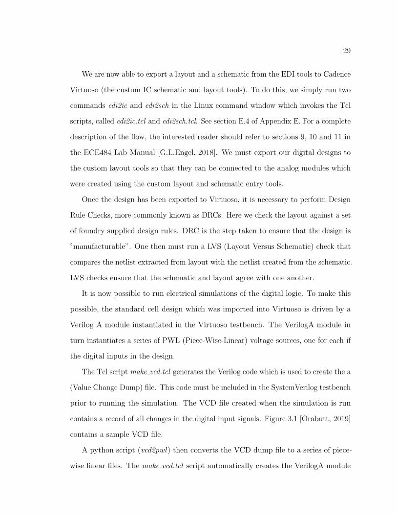
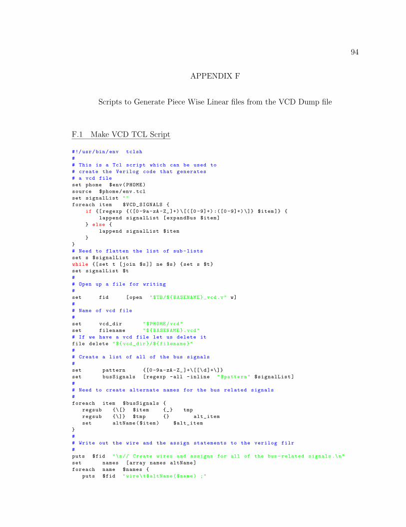
The Tcl script make vcd.tcl generates the Verilog code which is used to create the a
(Value Change Dump) file. This code must be included in the SystemVerilog testbench
prior to running the simulation. The VCD file created when the simulation is run
contains a record of all changes in the digital input signals. Figure 3.1 [Orabutt, 2019]
contains a sample VCD file.
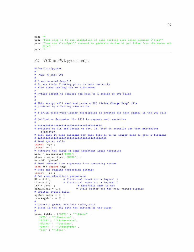
A python script (vcd2pwl) then converts the VCD dump file to a series of piece-
wise linear files. The make vcd.tcl script automatically creates the VerilogA module
Page 40
30
described above. The user only needs to create a symbol for the VerilogA module
before it can be instantiated into the Virtuoso testbench. The rise/fall times, scale
factors and logic levels for the analog signals can be specified in the python script.
See section F.2 of Appendix F. The standard PWL file format is a time-voltage pair
separated by space.
Figure 3.1: An example of a VCD file
Page 41
31
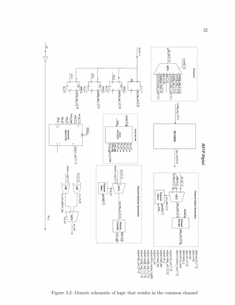
3.2 Configuration and Readout Electronics
The configuration and readout electronics provide control for all sixteen signal
processing channels. The common channel has three 8-bit configuration registers which
supports 24 configuration bits in total. These configuration registers are selectively
loaded to configure the HINP5 chip. The readout circuits allow for the analog pulse
trains along with there synchronized digital channel addresses to be transmitted to
the FPGA on the CB.
As shown in Figure 3.2, the common channel digital circuits (configuration and
readout) consists of an address register, three 8-bit configuration registers, a 16-bit
shadow register, mode decoding circuitry, OR generation, a 4-to-16 decoder, and
channel address/channel select generation circuits.
Note: Any bold-faced word in this chapter corresponds to the signal name in the
Verilog code of that particular module. The full Verilog description of the digital
modules discussed in this chapter can be found in section A.1 of Appendix A.
3.2.1 Address Register
The address register is an 8-bit register, ad reg, in the common channel that is
used to register address and mode information on the rising edge of stb. This register
resets asynchronously the on falling edge of reset L which is the master reset signal
for the HINP5 chip. The lower nybble contains the mode and the upper nybble the
address.
ad reg ← {address,mode} (3.1)
The address and mode information which is loaded into ad reg comes from an
8-bit wide ad in bus. The address register is a positive edge-triggered D-register
Page 42
32
Figure 3.2: Generic schematic of logic that resides in the common channel
Page 43
33
which is clocked by stb and asynchronously reset when the master reset (reset L)
signal goes low.
3.2.2 Configuration Registers
There are three 8-bit configuration registers config reg 0, config reg 1, and
config reg 2 located in the common channel. The enable signal of the specified
configuration register is active when that particular register address and mode is
selected. The data present on the 8-bit wide ad in bus will be loaded into that
designated register on the falling edge of the stb. As the standard cells library
contains only a positive edge triggered register, the configuration registers are clocked
with stb L which is an inverted form of the stb i.e. an active low stb signal.
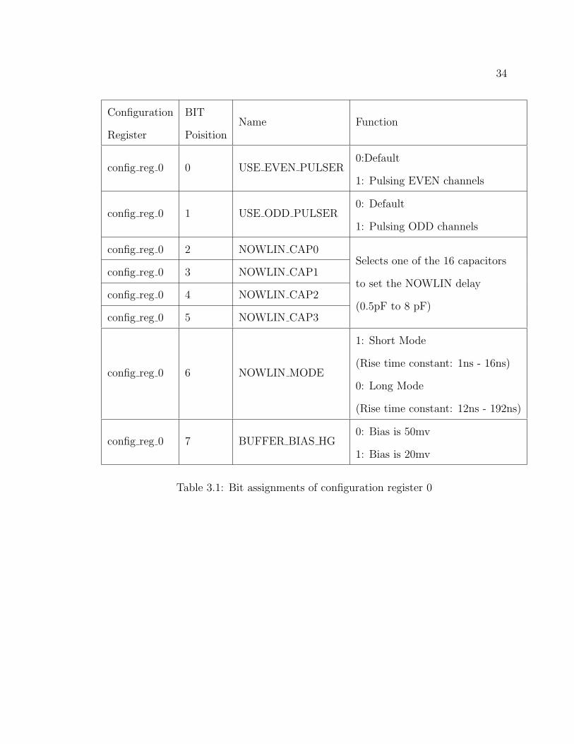
The three configuration registers holds 24 bits in total. The bit assignments
of Configuration Register 0 are given in the Table 3.1. The bit assignments of
Configuration Register 1 are provided in Table 3.2. Finally, the bit assignments for
Configuration Register 2 are presented in Table 3.3. All three configuration registers
are asynchronously reset when the master reset reset L signal goes low.
Page 44
34
Configuration
Register
BIT
PoisitionName Function
config reg 0 0 USE EVEN PULSER0:Default
1: Pulsing EVEN channels
config reg 0 1 USE ODD PULSER0: Default
1: Pulsing ODD channels
config reg 0 2 NOWLIN CAP0Selects one of the 16 capacitors
to set the NOWLIN delay
(0.5pF to 8 pF)
config reg 0 3 NOWLIN CAP1
config reg 0 4 NOWLIN CAP2
config reg 0 5 NOWLIN CAP3
config reg 0 6 NOWLIN MODE
1: Short Mode
(Rise time constant: 1ns - 16ns)
0: Long Mode
(Rise time constant: 12ns - 192ns)
config reg 0 7 BUFFER BIAS HG0: Bias is 50mv
1: Bias is 20mv
Table 3.1: Bit assignments of configuration register 0
Page 45
35
Configuration
Register
BIT
PositionName Function
config reg 1 0 BUFFER BIAS HG POL0: Positive Polarity
1: Negative Polarity
config reg 1 1 BUFFER BIAS LG0: Bias is 50mv
1: Bias is 20mv
config reg 1 2 BUFFER BIAS LG POL0: Positive Polarity
1: Negative Polarity
config reg 1 3 AUTO PEAK0: Use take event in peak detector
1: Use comparator output
config reg 1 4 SEL SHAPER0: Routes peak detector to output
1: Routes shaper signal to output
config reg 1 5 AGND TR0Allows to adjust AGND voltage
(1.4 to 1.8v in 50mV step)config reg 1 6 AGND TR1
config reg 1 7 AGND TR2
Table 3.2: Bit assignments of configuration register 1
Page 46
36
Configuration
Register
BIT
PositionName Function
config reg 2 0 TVC 2 USEC MODE0: TVC 500 nsec range
1: TVC 2 usec full range
config reg 2 1 EXT CHARGE AMP0: Use internal charge amp
1: Use external charge amp
config reg 2 2 HOLES0: Electrons Collection
1: Holes Collection
config reg 2 3 DLY VC04 bit value that determines the
16 delay times by the auto reset block
before the channels auto reset.
config reg 2 4 DLY VC1
config reg 2 5 DLY VC2
config reg 2 6 DLY VC3
config reg 2 7 DLY VC4
1 bit that determines the width of the
digital reset to be either 100nsec
or 1usec
Table 3.3: Bit assignments of configuration register 2
Page 47
37
3.2.3 Mode Decoding Circuitry
On the rising edge of stb, the write signal selects whether data needs to be
written into a register or read out of a register. Specifically, when the write signal is
high then depending on the mode, the configuration data will be written into the
appropriate configuration register, shadow register, or dac register in the designated
channel. The data transfer occurs on the falling edge of the stb. If write is low then
depending on the mode, the appropriate register will be read out of the chip.
Mode decoding circuitry is shown in Figure 3.3. It is composed of a mode decoder
and a multiplexer block which implements combinational logic used to compare the
write, mode and address bits with the encoded logic in them and performs the
specified operation. Initially, the address and mode information present on the 8-bit
wide ad in data bus is loaded into the address register on the rising edge of stb. Then
these address and mode bits are compared with the hard-coded logic implemented
in the mode decoder and multiplexer circuits.
Figure 3.3: Mode Decoding Logic implementation in common channel
Mode Decoder: The hard-coded values in the mode decoder are set to match the
four mode bits and write signal on the chip that must select the specific register. In
Page 48
38
addition it also matches the address of the channel the register is present then the
specified register’s enable signal is made active to write 8-bit configuration data into
the designated register on the falling edge of the stb.
The en cr0 signal is an enable used to load data into Configuration Register
0. The en cr1 signal is an enable used to load data into Configuration Register 1.
The en cr2 signal is an enable used to load data into Configuration Register 2. The
load dac signal is an enable used to write configuration data into the DAC register
in the channel pointed to by the address bits. The read dac signal is used to read
the contents of the DAC register of the selected channel. The en sr0 is an enable
used to load the lower 8 bits of the shadow register with data, whereas en sr1 is an
enable used to load the upper 8 bits of the shadow register with data on the 8-bit
ad in bus coming from the FPGA. The drive output buffer signal is sent to all
the sixteen signal channels and is used to readout the selected channel.
Multiplexer: The Multiplexer is used to select one of the eight input lines. The lower
three bits of mode is the control bus that is used to select which input should be
connected to ad out which is an 8-bit output bus used to send digital data to the
FPGA from the HINP5 chip. The various modes of operation are detailed in Table
3.4.
Page 49
39
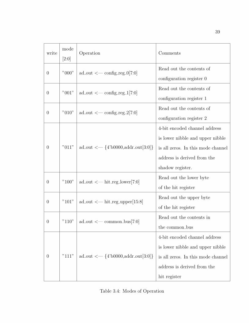
writemode
[2:0]Operation Comments
0 ”000” ad out <— config reg 0[7:0]Read out the contents of
configuration register 0
0 ”001” ad out <— config reg 1[7:0]Read out the contents of
configuration register 1
0 ”010” ad out <— config reg 2[7:0]Read out the contents of
configuration register 2
0 ”011” ad out <— {4’b0000,addr out[3:0]}
4-bit encoded channel address
is lower nibble and upper nibble
is all zeros. In this mode channel
address is derived from the
shadow register.
0 ”100” ad out <— hit reg lower[7:0]Read out the lower byte
of the hit register
0 ”101” ad out <— hit reg upper[15:8]Read out the upper byte
of the hit register
0 ”110” ad out <— common bus[7:0]Read out the contents in
the common bus
0 ”111” ad out <— {4’b0000,addr out[3:0]}
4-bit encoded channel address
is lower nibble and upper nibble
is all zeros. In this mode channel
address is derived from the
hit register
Table 3.4: Modes of Operation
Page 50
40
1 ”000” config reg 0 <— ad in[7:0]Loads configuration
register 0 (on posedge stb L)
1 ”001” config reg 1 <— ad in[7:0]Loads configuration
register 1 (on posedge stb L)
1 ”010” config reg 2 <— ad in[7:0]Loads configuration
register 2 (on posedge stb L)
1 ”011” addr in <— ad in[7:4]4-bit channel address supplied
by the FPGA
1 ”100” shadow reg lower <— ad in[7:0]
Loads lower byte of the shadow
register (on posedge stb L) with
data from the FPGA
1 ”101” shadow reg upper <— ad in[7:0]
Loads upper byte of the shadow
register (on posedge stb L) with data
from the FPGA
1 ”110” dac reg(addr) <— ad in[7:0]
Loads dac register in channel
pointed to by addr
(i,e upper 4 bits of ad reg).
Uses the load dac signal and
the sel chan[15:0] vector
1 ”111” addr in <— ad in[7:4]4-bit channel address supplied
by the FPGA
Table 3.5: Modes of Operation Continued
Page 51
41
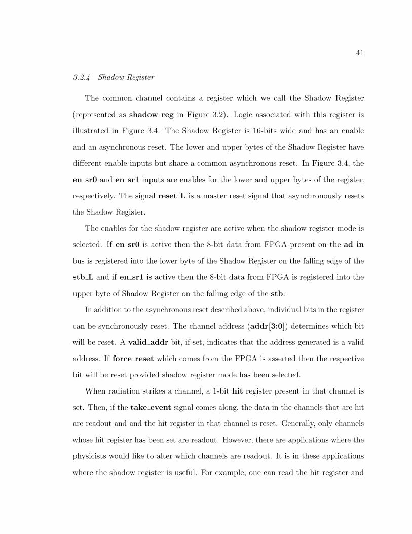
3.2.4 Shadow Register
The common channel contains a register which we call the Shadow Register
(represented as shadow reg in Figure 3.2). Logic associated with this register is
illustrated in Figure 3.4. The Shadow Register is 16-bits wide and has an enable
and an asynchronous reset. The lower and upper bytes of the Shadow Register have
different enable inputs but share a common asynchronous reset. In Figure 3.4, the
en sr0 and en sr1 inputs are enables for the lower and upper bytes of the register,
respectively. The signal reset L is a master reset signal that asynchronously resets
the Shadow Register.
The enables for the shadow register are active when the shadow register mode is
selected. If en sr0 is active then the 8-bit data from FPGA present on the ad in
bus is registered into the lower byte of the Shadow Register on the falling edge of the
stb L and if en sr1 is active then the 8-bit data from FPGA is registered into the
upper byte of Shadow Register on the falling edge of the stb.
In addition to the asynchronous reset described above, individual bits in the register
can be synchronously reset. The channel address (addr[3:0]) determines which bit
will be reset. A valid addr bit, if set, indicates that the address generated is a valid
address. If force reset which comes from the FPGA is asserted then the respective
bit will be reset provided shadow register mode has been selected.
When radiation strikes a channel, a 1-bit hit register present in that channel is
set. Then, if the take event signal comes along, the data in the channels that are hit
are readout and and the hit register in that channel is reset. Generally, only channels
whose hit register has been set are readout. However, there are applications where the
physicists would like to alter which channels are readout. It is in these applications
where the shadow register is useful. For example, one can read the hit register and
Page 52
42
based on its contents decide which channels to read out and then write to the shadow
register. The shadow register can then be used in the readout process.
Figure 3.4: Shadow Register
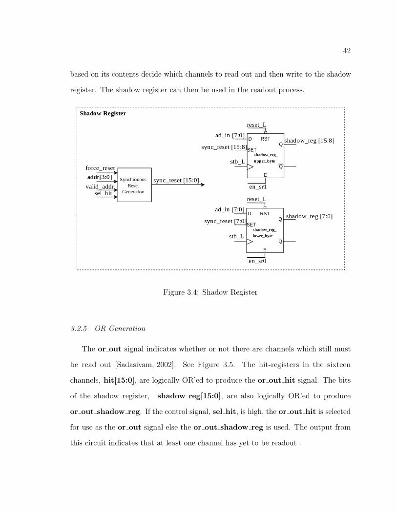
3.2.5 OR Generation
The or out signal indicates whether or not there are channels which still must
be read out [Sadasivam, 2002]. See Figure 3.5. The hit-registers in the sixteen
channels, hit[15:0], are logically OR’ed to produce the or out hit signal. The bits
of the shadow register, shadow reg[15:0], are also logically OR’ed to produce
or out shadow reg. If the control signal, sel hit, is high, the or out hit is selected
for use as the or out signal else the or out shadow reg is used. The output from
this circuit indicates that at least one channel has yet to be readout .
Page 53
43
Figure 3.5: Circuit that generates OR OUT signal
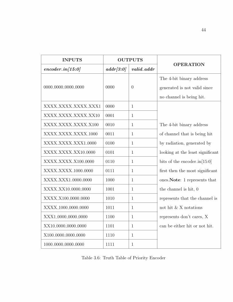
3.2.6 Channel Address Generation Circuitry
The Channel Address Generation (CAG) circuit produces a 4-bit channel address.
See Figure 3.6. Channels are encoded by a priority encoder. The lower channel
number, the higher priority. The input to the priority encoder is either 16-bit hit
register or the 16-bit shadow register. The sel hit determines which one. This sel hit
control signal of 1-bit, selects one of the two inputs to the output line in the 2-1
multiplexer. Our logic includes a flag, valid addr, which indicates whether or not
the channel address 0 is valid. The operation of the CAG module is summarized in
Table 3.6.
Figure 3.6: Channel Address Generation Circuit
Page 54
44
INPUTS OUTPUTSOPERATION
encoder in[15:0] addr[3:0] valid addr
0000 0000 0000 0000 0000 0
The 4-bit binary address
generated is not valid since
no channel is being hit.
XXXX XXXX XXXX XXX1 0000 1
The 4-bit binary address
of channel that is being hit
by radiation, generated by
looking at the least significant
bits of the encoder in[15:0]
first then the most significant
ones.Note: 1 represents that
the channel is hit, 0
represents that the channel is
not hit & X notations
represents don’t cares, X
can be either hit or not hit.
XXXX XXXX XXXX XX10 0001 1
XXXX XXXX XXXX X100 0010 1
XXXX XXXX XXXX 1000 0011 1
XXXX XXXX XXX1 0000 0100 1
XXXX XXXX XX10 0000 0101 1
XXXX XXXX X100 0000 0110 1
XXXX XXXX 1000 0000 0111 1
XXXX XXX1 0000 0000 1000 1
XXXX XX10 0000 0000 1001 1
XXXX X100 0000 0000 1010 1
XXXX 1000 0000 0000 1011 1
XXX1 0000 0000 0000 1100 1
XX10 0000 0000 0000 1101 1
X100 0000 0000 0000 1110 1
1000 0000 0000 0000 1111 1
Table 3.6: Truth Table of Priority Encoder
Page 55
45
3.2.7 Channel Select Generation Circuitry
The Channel Select Generation (CSG) circuit generates a 16-bit wide channel
select bus, chan sel. Each bit of the chan sel bus goes into one of the 16 signal
processing channels. For example, the chan sel bit of the specified channel must be
active to write the data from the FPGA into the channel’s DAC register. There are
several different circuits within a channel which need the channel select.
There are three sources for the channel addresses used to generate the channel
selects. These are ad in, addr, ad reg out. See Figure 3.7. The appropriate 4-bit
channel address is selected depending on the mode and write signals. Then, based
on the channel address, one of the 16 channel select lines will be active. However, if
the most significant bit of the mode bus is active then all the channel select lines will
be active.
Figure 3.7: Channel Select Generation Circuit
Page 56
46
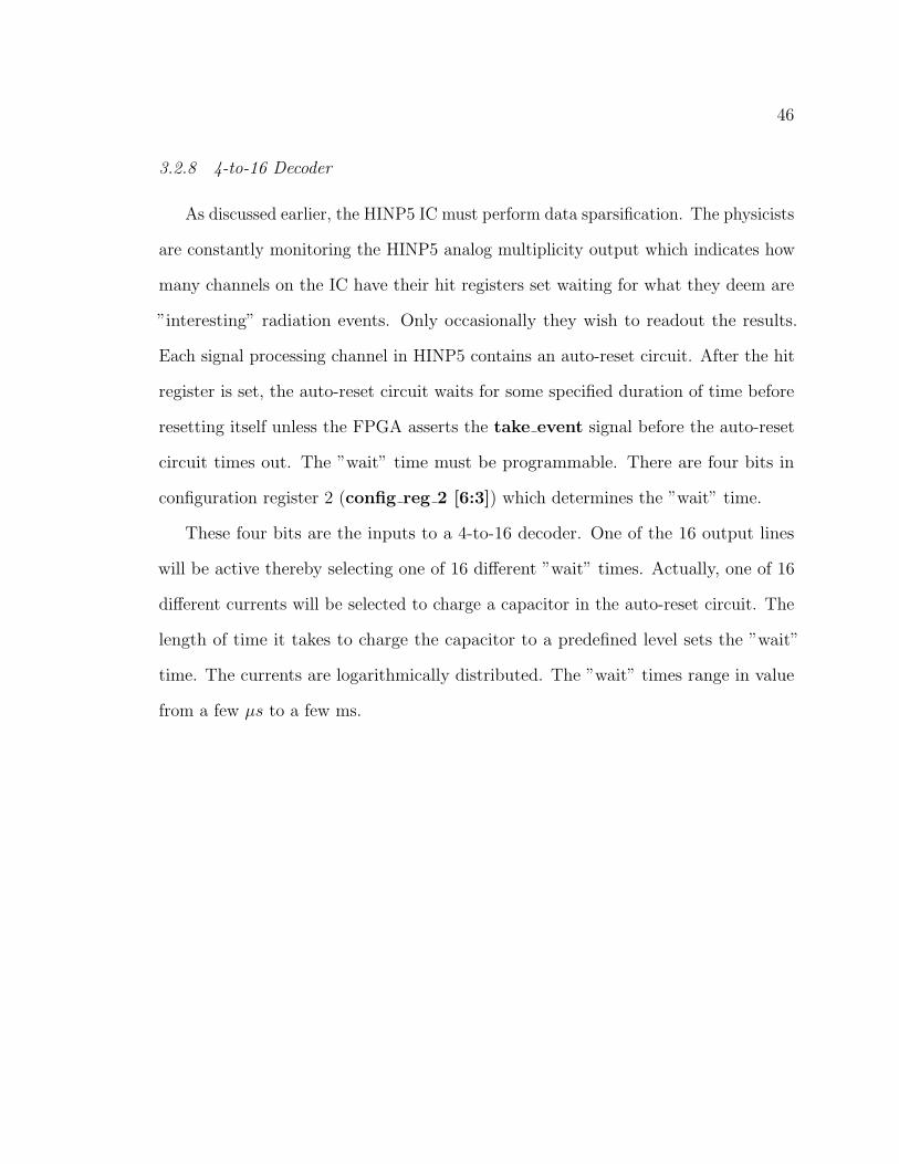
3.2.8 4-to-16 Decoder
As discussed earlier, the HINP5 IC must perform data sparsification. The physicists
are constantly monitoring the HINP5 analog multiplicity output which indicates how
many channels on the IC have their hit registers set waiting for what they deem are
”interesting” radiation events. Only occasionally they wish to readout the results.
Each signal processing channel in HINP5 contains an auto-reset circuit. After the hit
register is set, the auto-reset circuit waits for some specified duration of time before
resetting itself unless the FPGA asserts the take event signal before the auto-reset
circuit times out. The ”wait” time must be programmable. There are four bits in
configuration register 2 (config reg 2 [6:3]) which determines the ”wait” time.
These four bits are the inputs to a 4-to-16 decoder. One of the 16 output lines
will be active thereby selecting one of 16 different ”wait” times. Actually, one of 16
different currents will be selected to charge a capacitor in the auto-reset circuit. The
length of time it takes to charge the capacitor to a predefined level sets the ”wait”
time. The currents are logarithmically distributed. The ”wait” times range in value
from a few µs to a few ms.
Page 57
47
CHAPTER 4
SIGNAL CHANNEL
The digital modules in each signal processing channel consists of Hit Register, Auto
Reset Generation, Analog Reset Generation, and DAC as shown in Figure 4.5. Any
boldfaced word in this chapter corresponds to the signal name in the Verilog code of
that particular module. The Verilog description of the digital modules discussed in
this chapter can be found in section A.2 of Appendix A.
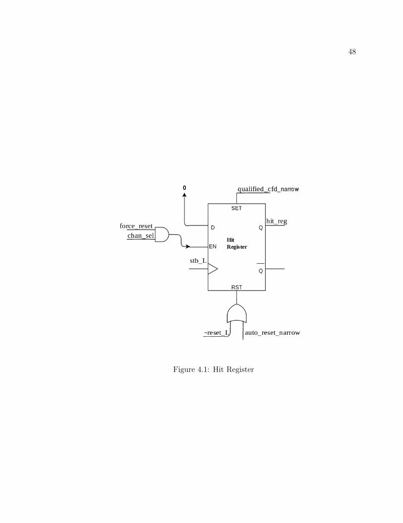
4.1 Hit Register
There is a 1-bit hit register in each of the signal channels represented as hit reg in
Figure 4.5. The hit register as shown in Figure 4.1 is a positive edge triggered D-register
with an enable, asynchronous reset and an asynchronous set. The hit register present in
the channel gets set asynchronously if a narrow trigger pulse (qualified cfd narrow)
comes from the CFD circuit which indicates that the channel has been hit. Trigger
pulses are only possible when the channel is enabled (both global and channel enables
are set). The qualified cfd signal is also active when the acq all signal (data acquisition
of all channels) is asserted by the FPGA. Note: acq all is ignored if the enables are
not active.
The hit register is reset synchronously if the force reset signal is asserted. It can
be asynchronously reset either a auto reset narrow pulse if the take event doesn’t
come along after waiting for some specified time (as described in the previous chapter)
or by an external (reset L) pulse.
During readout, data is read from the channels that have been hit when the
take event signal is asserted. Once, the data in a particular channel is read, the hit
register in that channel is reset. Readout continues until the or out goes inactive.
Page 58
48
Figure 4.1: Hit Register
Page 59
49
The outputs from the hit registers in the 16 signal channels form a bus (hit[15:0]).
4.2 Auto Reset Generation
The auto reset generation logic produces an auto reset pulse that automatically
resets the digital and analog circuits present in the signal processing channel if the
take event is not asserted after waiting for a specified ”wait” time. This circuit is
presented in Figure 4.2. Note: The vari one shot L signal in the Figure 4.2 is the
timeout signal from autoreset analog circuit as discussed in the previous chapter.
Figure 4.2: Auto Reset Generation Circuitry
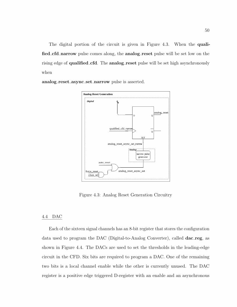
4.3 Analog Reset Generation
This analog reset signal is used to reset the analog circuits (for example, the
capacitors in the TVC and the peak detector circuits) present in the signal processing
channel. The analog reset signal will be asserted either if the auto reset pulse comes
along or the channels are forced to reset (external signal from FPGA).
Page 60
50
The digital portion of the circuit is given in Figure 4.3. When the quali-
fied cfd narrow pulse comes along, the analog reset pulse will be set low on the
rising edge of qualified cfd. The analog reset pulse will be set high asynchronously
when
analog reset async set narrow pulse is asserted.
Figure 4.3: Analog Reset Generation Circuitry
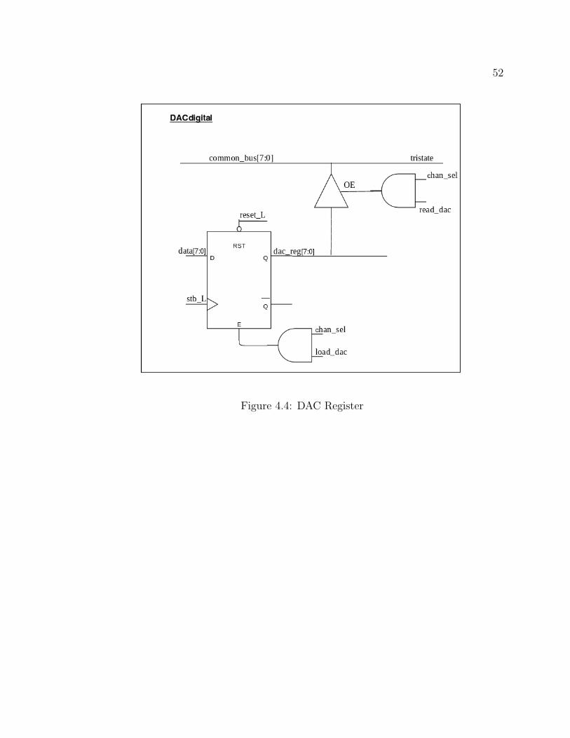
4.4 DAC
Each of the sixteen signal channels has an 8-bit register that stores the configuration
data used to program the DAC (Digital-to-Analog Converter), called dac reg, as
shown in Figure 4.4. The DACs are used to set the thresholds in the leading-edge
circuit in the CFD. Six bits are required to program a DAC. One of the remaining
two bits is a local channel enable while the other is currently unused. The DAC
register is a positive edge triggered D-register with an enable and an asynchronous
Page 61
51
reset. The control signals load dac, read dac and chan sel are generated in the
common channel (as discussed in the previous chapter).
As already discussed, on the rising edge of the stb the mode and address information
is stored in the address register. Based on the mode and channel address, on the falling
edge of stb the 8-bit data present on the ad in bus is loaded into the specified DAC
register (dac reg) in the designated channel. A DAC register is reset asynchronously
when reset L is active.
The DAC register in each signal channel can be loaded either with a different value
or the same value depending on the mode. One can even readout the contents of the
DAC register in the specified channel by choosing an appropriate mode. The 16 DAC
registers share an 8-bit wide tri-state bus, called common bus, driven by an enable
called (OE).
Please refer to Table 4.1 to learn more about the bit assignments of the DAC
register. Section A.3 of Appendix A to see a simple Verilog model for circuits which
are controlled by the logic described herein which lie outside of the digital block. This
allowed for a testbench to be created which could verify that all sixteen channels were
operating correctly.
Page 62
52
Figure 4.4: DAC Register
Page 63
53
BIT Poisition Name Function
0 DATA[0]
5 bit value that sets the threshold for the DAC
at what level cfd fires.
1 DATA[1]
2 DATA[2]
3 DATA[3]
4 DATA[4]
5 DATA[5]
This bit sets the polarity of the DAC
0: Positive Polarity
1: Negative Polarity
6 LOCAL ENA0: Disables the signal channel locally
1: Enables the signal channel locally
7 UNUSED UNUSED
Table 4.1: Bit assignments of DAC register in signal channel
Page 64
54
Figure 4.5: Generic schematic of the digital logic in the HINP5 signal channel
Page 65
55
CHAPTER 5
SUMMARY. CONCLUSIONS, AND FUTURE WORK
5.1 Summary
This thesis describes the design of the configuration and readout electronics for a
multi-channel integrated circuit (IC) which is used in the detection and monitoring
of ionizing radiation in low- and intermediate-energy nuclear physics experiments.
The sixteen channel chip discussed in this thesis can be used in a wide variety of
nuclear physics applications and is suitable for use whenever silicon strip detectors
are employed.
The chip can be used to determine the energy of a charged particle striking the
detector, as well as, the the time interval between the arrival of the particle at the
detector and an externally supplied time reference. The configuration and readout
circuits, common to all of the sixteen signal processing channels, as well as the digital
logic contained within a single signal processing channel, was implemented using the
Verilog Hardware Description Language (HDL) and a 0.35 µm standard cell library.
The IC is configured via three 8-bit configuration registers. Moreover, each channel
contains a 6-bit Digital-to-Analog Converter (DAC) which must be programmed to set
a threshold used by the Constant Fraction Discriminator (CFD), located in the timing
branch within each channel. The IC supports data sparsification where a channel
automatically resets itself (after a programmable delay time) unless explicitly directed
to enter readout mode by an externally generated control signal.
5.2 Conclusions
The Verilog-driven design described in this thesis was implemented using Ca-
dence’s EDI (Encounter Digital Implementation) tools for synthesis and place n’ route.
Page 66
56
Extensive simulations were performed using the NC-Sim (Cadence HDL simulator)
on the digital logic which belongs to the common channel, as well as for, the logic
which is to reside in each of the 16 signal processing channels. The simulation results
are as expected for the various configuration and readout tasks which the IC must
support. The testbench code was implemented using SystemVerilog and allowed us to
successfully validate our designs.
The standard cell designs were also imported into Cadence’s Virtuoso custom
IC tools and validated at the electrical level. The inputs to the digital blocks were
driven by a verilogA module. The voltage sources in the module were instantiated as
standard SPICE PWL (Piece-Wise-Linear) sources. The associated PWL files for the
PWL voltage sources were generated using NC-Sim and a collection of Tcl/python
scripts that were developed by our research laboratory. These scripts were described
in detail in this thesis. The electrical simulation performance is also as expected and
matches with the simulation results obtained using NC-Sim.
The simulated performance indicates that the digital logic in the IC is working as
expected. The common channel digital occupies an area of 427 µm x 223 µm whereas
the channel digital in each of the sixteen signal channels occupies an area of 191 µm
x 119 µm. The HINP5 IC will be fabricated using the AMS 0.35 micron NWELL
process. The layout of the circuits discussed in this thesis are given in Figures 5.1 and
5.2.
In conclusion, the use of the standard cell methodology greatly reduced the time
required to design these crucial digital circuits, but more importantly it makes it easy
for the design to be modified if errors are detected when the digital logic is integrated
with the analog blocks or if a new feature must be added late in our design cycle.
Since the digital logic was described using Verilog HDL, an up-to-date layout can be
generated literally within minutes after changing the Verilog source code!
Page 67
57
5.3 Future Work
Currently, the configuration and readout digital circuits implemented in this thesis
have a minimal set of SDC (Synopsis Design Constraints) timing and design constraints,
but there is need to enhance the current SDC constraints file to ensure that the design
is robust. These additional constraints should more accurately describe the circuits
that are driving the inputs of the common channel and signal channel digital circuits.
They must also better characterize the loads that are driven by these digital circuits.
These constraints will be added once the analog blocks have been completed and layed
out.
Also, as discussed in Chapter 2 of this thesis, the digtal logic described in this
thesis must interface to an FPGA on the chipboard. The FPGA design employs the
PicoBlaze soft core. Significant changes will need to be made to the existing PicoBlaze
code to make it compatible with the digital configuration and readout electronics
described herein. It should be noted that the digital logic described in this thesis is
significantly different than the logic associated with earlier versions of the HINP chip.
Moreover, the configuration and readout digital circuits needs to be integrated
with the bias circuits in the common channel and the linear and timing branches in
the signal processing channel to develop the complete HINP5 integrated circuit. The
layouts of the HINP5 circuits need to be finished. Then, more detailed chip level
simulations (including parasitic capacitance) need to be performed to ensure that
HINP5 is working as expected before the chip is submitted for fabrication. When the
chip is returned from fabrication, its performance will need to be characterized.
The HINP5 (Heavy Ion Nuclear Physics chip - Version 5) IC, is expected to be
Page 68
58
Figure 5.1: Layout of the HINP common channel digital logic generated by the place
n route tool
Page 69
59
Figure 5.2: Layout of the HINP signal channel digital logic generated by the place n
route tool
Page 70
60
fabricated using the AMS (Austrian Microsystems) 0.35 µm CMOS process in the
Fall of 2019. It is expected to arrive back from fabrication in Spring 2020.
Page 71
61
REFERENCES
[ADC, ] LTC1864/LTC1865 Power, 16-Bit, 250ksps 1- and 2-Channel ADCs inMSOP. Linear Technology.
[UG1, 2008] (2008). PicoBlaze 8-bit Embedded Microcontroller User Guide. Xilinx.v1.1.2.
[DS5, 2014] (2014). Spartan-3AN FPGA Family Data Sheet. Xilinx.
[B.S. Budden, 2015] B.S. Budden, L.C.Stonehill, A. (2015). Handheld readout elec-tronics to fully exploit the particle discrimination capabilities of elpasolitescintillators. Nuclear Instruments and Methods in Physics.
[Burla, 2019] Burla, J. (2019). Design and analysis of the timing branch of anintegrated circuit for use in nuclear physics experiments employing si-stripdetectors. Master’s thesis, Southern Illinois University Edwardsville.
[Engel, 2016] Engel, G. (2016). A multi-channel discriminator ic. http://www.siue.edu/~gengel/ece584WebStuff/CFDchip.pdf. accessed : 2017-1-10.
[Eriksson et al., 2019] Eriksson, H., Henriksson, T., Svensson, C., and Larsson-Edefors, P. (2019). Full-custom vs. standard-cell design flow a quantitativeadder comparison.
[G. Engel, 2007] G. Engel, M. Sadasivam, M. N. (2007). Multi-channel integratedcircuit for use in low and intermediate energy nuclear physics - hinp16c. NuclearInstruments and Methods in Physics.
[G.L.Engel, 2018] G.L.Engel (2018). ECE484 AMS HITKIT Tutorial-Version 4.1.Southern Illinios University Edwardsville.
[G.L.Engel et al., 2009] G.L.Engel, M.J.Hall, Proctor, J., Elson, J., L.G.Sobotka,R.Shane, and Charity, R. (2009). Design and performance of a multi-channel,multi-sampling, psd-enabling integrated circuit. Nuclear Instruments and Meth-ods in Physics.
[Helmuth, 2005] Helmuth, S. (2005). Semiconductor Detector Systems. Oxford Uni-versity Press, New York.
[I. Tilquin, 1995] I. Tilquin, Y. El Masri, M. P. (1995). Detection efficiency of the neu-tron modular detector demon and related characteristics. Nuclear Instrumentsand Methods in Physics.
[Korkmaz, 2019] Korkmaz, A. (2019). Design and analysis of the linear branch ofan integrated circuit for use in nuclear physics experiments employing si-stripdetectors. Master’s thesis, Southern Illinois University Edwardsville.
Page 72
62
[N. Zaitseva, 2012] N. Zaitseva, B. L. Rupert, I. P. (2012). Plastic scintillators withefficient neutron/gamma pulse shape discrimination author links open overlaypanel. Nuclear Instruments and Methods in Physics.
[Orabutt, 2019] Orabutt, B. (2019). Design and analysis of a multi-channel discrimi-nator integrated circuit for use in nuclear physics experiments. Master’s thesis,Southern Illinois University Edwardsville.
[Proctor, 2007] Proctor, J. (2007). Design of a multi-channel integrated circuit for usein nuclear physics experiments where particle identification is required. Master’sthesis, Southern Illinois University Edwardsville.
[Rabaey, 2003] Rabaey, J. (2003). Digital integrated circuits : a design perspective.Pearson Education, Upper Saddle River, N.J.
[Sadasivam, 2002] Sadasivam, M. (2002). A multi-channel integrated circuit for usewith silicon strip detectors in experiments in low and intermediate physics.Master’s thesis, Southern Illinois University Edwardsville.
[Tsividis, 2011] Tsividis, Y. (2011). Operation and modeling of the MOS transistor.Oxford University Press, New York.
[Weste, 2006] Weste, N. (2006). CMOS VLSI Ddesign: A Circuits and SystemsPerspective. Pearson Education, Delhi.
Page 73
63
APPENDIX A
Verilog Description of Digital Design Implemented in HINP5
A.1 Verilog description of the digital circuits in common channel
// This is Verilog that describes digital logic in HINP5
‘timescale 1ns/100ps
module HINPdigital(input [7:0] ad_in ,
input write ,
input stb ,
input reset_L ,
input [15:0] hit ,
input force_reset ,
input tri [7:0] common_bus ,
output reg [7:0] ad_out ,
output or_out ,
output reg [15:0] chan_sel ,
output reg drive_output_buffer ,
output reg load_dac ,
output reg read_dac ,
output reg [7:0] config_reg_0 ,
output reg [7:0] config_reg_1 ,
output reg [7:0] config_reg_2 ,
output reg [15:0] dec_out ,
input stb_L
);
// Register for Address and Mode Information
// Asynchronous Reset
// Clocked of postive edge strobe
reg [3:0] chan_addr;
wire [3:0] mode;
wire [7:0] ad;
reg [7:0] ad_reg_out;
reg en_cr0 , en_cr1 , en_cr2 , en_sr0 , en_sr1;
always @(posedge stb or negedge reset_L) begin
if (~ reset_L) ad_reg_out <= 8’d0;
else if (stb) ad_reg_out <= ad_in;
end
assign mode = ad_reg_out [3:0];
// We need three 8-bit configuration registers
// Configuration Register 0 holds: config_reg_0 [0]= USE_EVEN_PULSER; config_reg_0 [1]=
USE_ODD_PULSER;config_reg_0 [2]= NOWLIN_CAP0;
// config_reg_0 [3]= NOWLIN_CAP1; config_reg_0 [4]=
NOWLIN_CAP2; config_reg_0 [5]= NOWLIN_CAP3;
// config_reg_0 [6]= NOWLIN_MODE; config_reg_0 [7]= BUFFER_BIAS_HG;
always @(posedge stb_L or negedge reset_L) begin
if (~ reset_L) config_reg_0 <= 8’d0;
else if (en_cr0) config_reg_0 <= ad_in;
end
// Configuration Register 1 holds: config_reg_1 [0]= BUFFER_BIAS_LG; config_reg_1 [1]=
BUFFER_BIAS_TVC;config_reg_1 [2]= UNUSED;
// config_reg_1 [3]= UNUSED; config_reg_1 [4]= UNUSED;
config_reg_1 [5]= AGND_TR0;
// config_reg_1 [6]= AGND_TR1; config_reg_1 [7]= AGND_TR2;
always @(posedge stb_L or negedge reset_L) begin
Page 74
64
if (~ reset_L) config_reg_1 <= 8’d0;
else if (en_cr1) config_reg_1 <= ad_in;
end
// Configuration Register 2 holds: config_reg_2 [0]= TVC_2_USEC_MODE; config_reg_2 [1]=
UNUSED;config_reg_2 [2]= UNUSED;
// config_reg_2 [3]= DLY_VC0; config_reg_2 [4]= DLY_VC1; config_reg_2 [5]= DLY_VC2;
config_reg_2 [6]= DLY_VC3; config_reg_2 [7]= DLY_VC4;
always @(posedge stb_L or negedge reset_L) begin
if (~ reset_L) config_reg_2 <= 8’d0;
else if (en_cr2) config_reg_2 <= ad_in;
end
// Mode decoder
always @(mode [3:0] or write) begin
en_cr0 = ((~ mode [3] & mode [2:0] == 3’d0) & write)? 1’b1 : 1’b0;
en_cr1 = ((~ mode [3] & mode [2:0] == 3’d1) & write)? 1’b1 : 1’b0;
en_cr2 = ((~ mode [3] & mode [2:0] == 3’d2) & write)? 1’b1 : 1’b0;
en_sr0 = ((~ mode [3] & mode [2:0] == 3’d4) & write)? 1’b1 : 1’b0;
en_sr1 = ((~ mode [3] & mode [2:0] == 3’d5) & write)? 1’b1 : 1’b0;
load_dac = ((mode [3] == 1’b1 | mode [2:0] == 6) & write)? 1’b1: 1’b0;
read_dac = ((~ mode [3] & mode [2:0] == 3’d6) & ~write)? 1’b1 : 1’b0;
drive_output_buffer = ((mode [2:0] == 3’d3 | mode [2:0] == 3’d7) & ~write) ? 1’b1:
1’b0;
end
reg [3:0] addr;
// MUX Logic for choosing address ad_out
always @(*) begin
case (mode [2:0])
0: ad_out = config_reg_0;
1: ad_out = config_reg_1;
2: ad_out = config_reg_2;
3: ad_out = {4’b0000 ,addr [3:0]};
4: ad_out = hit [7:0];
5: ad_out = hit [15:8];
6: ad_out = common_bus [7:0];
7: ad_out = {4’b0000 ,addr [3:0]};
endcase
end
// MUX Logic for channel address
reg [1:0] sel_addr;
always @(*) begin
case (sel_addr)
0: chan_addr = ad_in [7:4];
1: chan_addr = addr [3:0];
2: chan_addr = ad_reg_out [7:4];
3: chan_addr = 4’b0000;
endcase
end
// Generate sel_addr
always @(*) begin
sel_addr = 2’d0;
if ((mode [2:0] == 3’d3 | mode [2:0] == 3’d7) & write ) sel_addr = 2’d0;
else if ((( mode [2:0] == 3’d3) | (mode [2:0] == 3’d7 )) & ~write) sel_addr = 2’d1;
else if (mode [2:0] == 3’d6) sel_addr = 2’d2;
end
// Instiantiate the Shadow register module created
reg [15:0] shadow_reg;
reg valid_addr;
wire sel_hit;
// reset_L is asynchronous reset signal
// force_reset is a synchronous signal
shadowreg sreg( .ad_in(ad_in),
.stb_L(stb_L),
Page 75
65
.reset_L(reset_L),
.force_reset(force_reset),
.en_sr0(en_sr0),
.en_sr1(en_sr1),
.addr(addr),
.sel_hit(sel_hit),
.valid_addr(valid_addr),
.shadow_reg(shadow_reg)
);
// MUX Logic for choosing either hit register or shadow register
reg [15:0] encoder_in;
always @(*) begin
case (sel_hit)
0: encoder_in = shadow_reg;
1: encoder_in = hit;
endcase
end
// Generate sel_hit bit for choosing either hit register or shadow register
assign sel_hit = (mode [2:0] == 3’d3 & ~write)? 1’b0 : 1’b1;
// Priority Encoder Block
integer j;
always @(*) begin
if (| encoder_in) begin
for (j=15; j>=0 ; j=j-1) begin
if (encoder_in[j]) begin
addr = j;
valid_addr = 1’b1;
end
end
end
else begin
addr = 4’d0;
valid_addr = 1’b0;
end
end
// Channel Decoder
always @(*) begin
chan_sel = 16’d0;
if (mode [2:0] == 3’d3 || mode [2:0] == 3’d7) begin
for (j=0; j<16 ; j=j+1) begin
if (chan_addr == j) begin
chan_sel[j] = 1’b1;
end
end
end
else if (mode [3] == 1’b1) chan_sel = 16’hFFFF;
else if (mode [2:0] == 3’d6) begin
for (j=0; j<16 ; j=j+1) begin
if (chan_addr == j) begin
chan_sel[j] = 1’b1;
end
end
end
end
wire [3:0] dec_in;
assign dec_in = config_reg_2 [6:3];
// 4 to 16 Decoder
always @(*) begin
case(dec_in)
4’b0000: dec_out = 16’ b0000_0000_0000_0001;
4’b0001: dec_out = 16’ b0000_0000_0000_0010;
4’b0010: dec_out = 16’ b0000_0000_0000_0100;
Page 76
66
4’b0011: dec_out = 16’ b0000_0000_0000_1000;
4’b0100: dec_out = 16’ b0000_0000_0001_0000;
4’b0101: dec_out = 16’ b0000_0000_0010_0000;
4’b0110: dec_out = 16’ b0000_0000_0100_0000;
4’b0111: dec_out = 16’ b0000_0000_1000_0000;
4’b1000: dec_out = 16’ b0000_0001_0000_0000;
4’b1001: dec_out = 16’ b0000_0010_0000_0000;
4’b1010: dec_out = 16’ b0000_0100_0000_0000;
4’b1011: dec_out = 16’ b0000_1000_0000_0000;
4’b1100: dec_out = 16’ b0001_0000_0000_0000;
4’b1101: dec_out = 16’ b0010_0000_0000_0000;
4’b1110: dec_out = 16’ b0100_0000_0000_0000;
4’b1111: dec_out = 16’ b1000_0000_0000_0000;
default: dec_out = 16’ b0000_0000_0000_0000;
endcase
end
// Need to know if any of the channel is hit , or_out gives this information
wire or_out_hit ,or_out_shadow_reg;
assign or_out_hit = |hit;
assign or_out_shadow_reg = |shadow_reg;
assign or_out = (sel_hit)? or_out_hit : or_out_shadow_reg;
endmodule
A.1.1 Verilog description of shadow register
module shadowreg( input [7:0] ad_in ,
input stb_L ,
input reset_L ,
input force_reset ,
input sel_hit ,
input valid_addr ,
input en_sr0 ,
input en_sr1 ,
input [3:0] addr ,
output reg [15:0] shadow_reg
);
genvar i ;
// reset_L is an asynchronous reset
// forece_reset causes a synchronous reset
wire [15:0] sync_reset;
// Create the synchronous reset signal
// COMBINATIONAL LOGIC
generate
for (i=0; i <=15; i=i+1) begin
assign sync_reset[i] = ((addr == i) & force_reset & ~sel_hit & valid_addr) ?
1’b1 : 1’b0;
end
endgenerate
// Implement lower and upper bytes of shadow register
generate
for (i=0; i<=15; i=i+1) begin
if (i <= 7) begin
always @(posedge stb_L or negedge reset_L) begin
if (~ reset_L) shadow_reg[i] <= 1’b0 ;
else if (sync_reset[i]) shadow_reg[i] <= 1’b0;
else if (en_sr0) shadow_reg[i] <= ad_in[i];
end
end
else if (i > 7 && i<=15) begin
always @(posedge stb_L or negedge reset_L) begin
Page 77
67
if (~ reset_L) shadow_reg[i] <= 1’b0 ;
else if (sync_reset[i]) shadow_reg[i] <= 1’b0;
else if (en_sr1) shadow_reg[i] <= ad_in[i-8];
end
end
end
endgenerate
endmodule
A.2 Verilog description of the digital circuits in a signal channel
//
// This is a verilog description of the HINP channel logic
//
module Channeldigital(input reset_L ,
input force_reset ,
input cfd_out ,
input [7:0] ad_in ,
input stb_L ,
input take_event ,
input global_ena ,
input acq_all ,
input chan_sel ,
input drive_output_buffer ,
input common_stop ,
input vari_one_shot_L ,
input spl_chan ,
input qualified_cfd_narrow ,
input auto_reset_narrow ,
input analog_reset_async_set_narrow ,
input load_dac ,
input read_dac ,
output qualified_cfd ,
output analog_reset_async_set ,
output reg auto_reset ,
output reg dont_charge_cap_L ,
output charge_cap_L ,
output reg analog_reset ,
output [7:0] common_bus ,
output reg [7:0] dac_reg ,
output read_chan ,
output hit
);
wire din_L;
wire din;
LOGIC0 L0(.Q(din_L));
LOGIC1 L1(.Q(din));
// Modelling DAC register
always @(posedge stb_L or negedge reset_L) begin
if (~ reset_L) dac_reg <= 8’d0;
else if (chan_sel & load_dac) dac_reg <= ad_in;
end
// Modelling tri state bus for DAC registers
assign common_bus = (( read_dac & chan_sel)|(~ read_dac & spl_chan))? dac_reg : 8’dz;
// Need to qualify the cfd signals
assign qualified_cfd = (( cfd_out | acq_all) & (global_ena & dac_reg [6]));
// Modelling Auto Reset Pulse
wire gen_auto_reset;
assign gen_auto_reset = vari_one_shot_L & ~take_event;
always @( posedge gen_auto_reset or posedge qualified_cfd_narrow ) begin
Page 78
68
if (qualified_cfd_narrow) auto_reset <= 1’b0;
else if (gen_auto_reset) auto_reset <= din;
end
// Modeling Hit Register in Channel
reg hit_reg;
wire hit_regs_sync_reset;
wire hit_regs_async_reset;
// Need to implement reset signals for the hit registers
// Asynchronous reset should occur as part of auto -reset or since the channel
// is selected and the force_reset signal is being applied from the FPGA.
assign hit_regs_sync_reset = (chan_sel & force_reset) ? 1’b1 : 1’b0;
assign hit_regs_async_reset = (~ reset_L | auto_reset_narrow) ? 1’b1 : 1’b0;
// Need to implement the hit registers
// CLocked off posegde of the qualified cfd signal and are asynchronously reset
always @( posedge stb_L or posedge hit_regs_async_reset or posedge
qualified_cfd_narrow) begin
if (hit_regs_async_reset) hit_reg <= 1’b0;
else if (qualified_cfd_narrow) hit_reg <= 1’b1;
else if (hit_regs_sync_reset) hit_reg <= din_L;
end
assign hit = hit_reg;
// Modelling Analog Reset Pulse
assign analog_reset_async_set = (( chan_sel & force_reset)|gen_auto_reset) ? 1’b1 : 1’
b0;
always @(posedge qualified_cfd_narrow or posedge analog_reset_async_set_narrow or
negedge reset_L) begin
if (~ reset_L) analog_reset <= 1’b1;
else if (analog_reset_async_set_narrow) analog_reset <= 1’b1;
else if (qualified_cfd_narrow) analog_reset <= din_L;
end
// Modelling TVC digital logic
wire dig_reset;
assign dig_reset = (common_stop | ~reset_L | (force_reset & chan_sel)) ? 1’b1 : 1’b0;
always @(posedge qualified_cfd_narrow or posedge dig_reset) begin
if (dig_reset) dont_charge_cap_L <= 1’b0;
else if (qualified_cfd_narrow) dont_charge_cap_L <= din;
end
assign charge_cap_L = ~dont_charge_cap_L;
// Modelling Digital Logic for Peak Sampler
assign read_chan = (drive_output_buffer & chan_sel)? 1’b1 : 1’b0;
endmodule
A.3 Verilog description of HINP channels
//
// This is a verilog behavioral model of the 16 HINP channels
//
module HINPchannels(input [15:0] cfd_out ,
input [7:0] data ,
input stb_L ,
input reset_L ,
input force_reset ,
input electron_collection ,
input [15:0] chan_sel ,
input load_dac ,
input read_dac ,
input drive_output_buffer ,
input common_stop ,
input acq_all ,
input global_ena ,
Page 79
69
input take_event ,
input [15:0] qualified_cfd_narrow ,
input [15:0] auto_reset_narrow ,
input [15:0] vari_one_shot_L ,
input [15:0] analog_reset_async_set_narrow ,
output reg [15:0] dont_charge_cap_L ,
output [15:0] charge_cap_L ,
output reg [15:0] analog_reset ,
output [15:0] analog_reset_async_set ,
output [15:0] auto_reset ,
output [15:0] qualified_cfd ,
output [7:0] common_bus ,
output [15:0] hit ,
output integer high_gain_shaper [15:0] ,
output integer low_gain_shaper [15:0] ,
output integer tvc [15:0]
);
// Need a genvar for the generate statements used
genvar i;
// Model the high_gain_shaper , low_gain_shaper and tvc outputs
// Send out an integer indicating the channel number (incremented by 1) and these
outputs should be high Z when not selected
generate
for (i=0;i<=15;i=i+1) begin
assign high_gain_shaper[i] = (chan_sel[i] & drive_output_buffer) ? i+1 : 1’bz;
assign low_gain_shaper[i] = (chan_sel[i] & drive_output_buffer) ? i+1 : 1’bz;
assign tvc[i] = (chan_sel[i] & drive_output_buffer) ? i+1 : 1’bz;
end
endgenerate
// These outputs all are reset to zero when the force_reset comes along
generate
for (i=0;i<=15;i=i+1) begin
assign high_gain_shaper[i] = (chan_sel[i] & force_reset) ? 1’b0 : 1’bz;
assign low_gain_shaper[i] = (chan_sel[i] & force_reset) ? 1’b0 : 1’bz;
assign tvc[i] = (chan_sel[i] & force_reset) ? 1’b0 : 1’bz;
end
endgenerate
// Need to implement the auto_reset signal
// When the cfd comes , we need to wait a while and if take_event doesn ’t some along
// within some specified time period then we should issue a auto_reset signal
// Model Digital Logic for 16 channels
reg [7:0] dac_regs [15:0];
wire [15:0] hit_regs_async_reset;
wire [15:0] hit_regs_sync_reset;
wire [15:0] hit;
wire [15:0] read_chan;
wire [15:0] spl_chan;
generate
for (i=0; i<=15 ; i=i+1) begin
assign spl_chan[i] = (i==0) ? 1’b1 : 1’b0;
end
endgenerate
generate
for (i=0; i<=15 ; i=i+1) begin
// Channel Digital Logic
Channeldigital chandigital( .reset_L(reset_L),
.force_reset(force_reset),
.cfd_out(cfd_out[i]),
.stb_L(stb_L),
.load_dac(load_dac),
.ad_in(data),
.read_dac(read_dac),
Page 80
70
.global_ena(global_ena),
.acq_all(acq_all),
.take_event(take_event),
.chan_sel(chan_sel[i]),
.spl_chan(spl_chan[i]),
.drive_output_buffer(drive_output_buffer),
.common_stop(common_stop),
.vari_one_shot_L(vari_one_shot_L[i]),
.qualified_cfd(qualified_cfd[i]),
.qualified_cfd_narrow(qualified_cfd_narrow[i]),
.auto_reset_narrow(auto_reset_narrow[i]),
.analog_reset_async_set_narrow(analog_reset_async_set_narrow[i
]),
.analog_reset_async_set(analog_reset_async_set[i]),
.auto_reset(auto_reset[i]),
.dont_charge_cap_L(dont_charge_cap_L[i]),
.charge_cap_L(charge_cap_L[i]),
.analog_reset(analog_reset[i]),
.dac_reg(dac_regs[i]),
.common_bus(common_bus),
.read_chan(read_chan[i]),
.hit(hit[i])
);
end
endgenerate
wire [15:0] local_ena;
generate
for (i=0; i<=15 ; i=i+1) begin
assign local_ena[i] = dac_regs[i][6];
end
endgenerate
endmodule
Page 81
71
APPENDIX B
System Verilog Test Fixture for Verification
B.1 SystemVerilog definition of global parameters
/* Characteristics of Pulse */
localparam PERIOD = 100ns;
localparam LENGTH_OF_RESET = 100ns;
localparam LENGTH_OF_FORCE_RESET = 100ns;
localparam DURATION_OF_COMMON_STOP = 50ns;
localparam WIDTH_OF_CFD_NARROW_PULSE = 50ns;
localparam SHORT_DELAY = 50ns;
localparam MEDIUM_DELAY = 1us;
localparam LONG_DELAY = 10us;
localparam DURATION_OF_READOUT = 1us;
localparam BITS = 8;
localparam CHAN = 16;
/* Config Registers Address and Mode Parameters */
localparam CR0 = 8’h0;
localparam CR1 = 8’h1;
localparam CR2 = 8’h2;
/* DAC Registers Address and Mode Parameters */
localparam DAC0 = 8’h06;
localparam DAC1 = 8’h16;
localparam DAC2 = 8’h26;
localparam DAC3 = 8’h36;
localparam DAC4 = 8’h46;
localparam DAC5 = 8’h56;
localparam DAC6 = 8’h66;
localparam DAC7 = 8’h76;
localparam DAC8 = 8’h86;
localparam DAC9 = 8’h96;
localparam DAC10 = 8’hA6;
localparam DAC11 = 8’hB6;
localparam DAC12 = 8’hC6;
localparam DAC13 = 8’hD6;
localparam DAC14 = 8’hE6;
localparam DAC15 = 8’hF6;
localparam DAC_ALL = 8’hF8;
/* Hit Channel Parameters */
localparam SEED = 16;
localparam RANDOM = 1;
localparam ALL = 2;
localparam NONE = 3;
localparam EVENS = 4;
localparam ODDS = 5;
localparam ACQ_ALL = 6;
/* Shadow Register Parameters */
localparam SR0 = 8’h04;
localparam SR1 = 8’h05;
localparam SHADOW_REG = 8’h03;
localparam HIT_REG = 8’h07;
localparam HR0 = 8’h04;
localparam HR1 = 8’h05;
localparam FPGA_ADDR = 8’hE;
Page 82
72
localparam WAIT_FOR_TAKE_EVENT = 2us;
localparam AUTO_RESET_WIDTH = 20us;
localparam NO_READOUT = 0;
localparam READOUT = 1;
B.2 SystemVerilog tasks
/*
################################
Initialization
################################
*/
task init;
stb = 1’b0;
fpga_out = 8’b0;
write = 1’b0;
force_reset = 1’b0;
cfd_out = 16’d0;
reset_L = 1’b1;
electron_collection = 1’b0;
common_stop = 1’b0;
acq_all = 1’b0;
global_ena = 1’b1;
take_event = 1’b0;
FPGA_reg = 16’d0;
master_rst;
endtask
/*
################################
Apply strobe signal
################################
*/
task apply_strobe;
stb = 1’b1;
#( PERIOD /2.0)
stb = 1’b0;
#( PERIOD /2.0);
endtask
/*
################################
Master Reset
################################
*/
task master_rst;
reset_L = 1’b0;
#( LENGTH_OF_RESET)
reset_L = 1’b1;
endtask
/*
################################
Apply common stop signal
################################
*/
task apply_common_stop;
common_stop = 1’b1;
#( DURATION_OF_COMMON_STOP)
common_stop = 1’b0;
endtask
/*
################################
Page 83
73
Holes collection
################################
*/
task collect_holes;
electron_collection = 1’b1;
endtask
/*
################################
Electrons collection
################################
*/
task collect_electrons;
electron_collection = 1’b0;
endtask
/*
################################
Apply Take Event signal
################################
*/
task take_event_high;
take_event = 1’b1;
endtask
task take_event_low;
take_event = 1’b0;
endtask
/*
################################
Apply acquistion all signal
################################
*/
task apply_acq_all;
acq_all = 1’b1;
#( SHORT_DELAY)
acq_all = 1’b0;
endtask
/*
################################
Apply global enable signal
################################
*/
task global_ena_high;
global_ena = 1’b1;
endtask
task global_ena_low;
global_ena = 1’b0;
endtask
/*
################################
Get strobe low
################################
*/
task strobe_low;
stb = 1’b0;
endtask
/*
################################
Get strobe high
################################
*/
task strobe_high;
stb = 1’b1;
endtask
Page 84
74
/*
########################################
Load configuration and DAC registers
########################################
*/
task config_register(input [7:0] reg_value , input [7:0] data);
global_ena_low;
#( PERIOD / 4.0);
strobe_low;
#( PERIOD / 4.0);
fpga_out = reg_value;
write = 1’b1;
#( PERIOD / 4.0);
strobe_high;
#( PERIOD / 4.0);
fpga_out = data;
#( PERIOD / 4.0);
strobe_low;
#( PERIOD / 4.0);
write = 1’b0;
global_ena_high;
endtask
/*
######################################
Read configuration and DAC registers
######################################
*/
task read_register(input [7:0] reg_value);
global_ena_low;
write = 1’b1;
#( PERIOD / 4.0);
strobe_low;
#( PERIOD / 4.0);
fpga_out = reg_value;
#( PERIOD / 4.0);
strobe_high;
#( PERIOD / 4.0);
write = 1’b0;
#( PERIOD / 4.0);
strobe_low;
#( PERIOD / 4.0);
write = 1’b1;
global_ena_high;
endtask
/*
######################################
Choose contents of shadow register
######################################
*/
task sel_shadowreg;
strobe_low;
#( PERIOD / 4.0);
fpga_out = SHADOW_REG;
#( PERIOD / 4.0);
strobe_high;
#( PERIOD / 2.0);
strobe_low;
endtask
/*
######################################
Choose contents of hit register
######################################
Page 85
75
*/
task sel_hitreg;
strobe_low;
#( PERIOD / 4.0);
fpga_out = HIT_REG;
#( PERIOD / 4.0);
strobe_high;
#( PERIOD / 2.0);
strobe_low;
endtask
/*
######################################
select external address from FPGA
######################################
*/
task sel_ext_addr(input [7:0] data);
strobe_low;
#( PERIOD / 4.0);
fpga_out = data;
write = 1’b1;
#( PERIOD / 4.0);
strobe_high;
#( PERIOD / 2.0);
strobe_low;
endtask
/*
#########################
Apply force reset signal
#########################
*/
task force_reset_high;
force_reset = 1’b1;
endtask
task force_reset_low;
force_reset = 1’b0;
endtask
/*
################################
Load Shadow register
################################
*/
task load_shadow_reg(input [7:0] byte_loc , input [7:0] data);
global_ena_low;
#( PERIOD / 4.0);
strobe_low ;
#( PERIOD / 4.0) ;
fpga_out = byte_loc ;
write = 1’b1 ;
#( PERIOD / 4.0) ;
strobe_high;
#( PERIOD / 4.0) ;
fpga_out = data ;
#( PERIOD / 4.0) ;
strobe_low ;
#( PERIOD / 4.0) ;
write = 1’b0 ;
global_ena_high;
endtask
/*
############################################################################
Clear particular channel bit in shadow register
############################################################################
Page 86
76
*/
task clr_shadow_reg_bit;
strobe_low ;
#( PERIOD / 4.0) ;
fpga_out = SHADOW_REG;
#( PERIOD / 4.0) ;
strobe_high ;
#( PERIOD / 4.0) ;
force_reset_high;
#( PERIOD / 4.0) ;
strobe_low ;
#( PERIOD / 4.0) ;
force_reset_low;
endtask
/*
######################################
Generate random value for cfd signals
######################################
*/
task random_cfd(integer seed);
cfd_out = $random ();
endtask
/*
######################################
Hit channels
######################################
*/
task hit_channels(input integer hit_type);
case (hit_type)
RANDOM: random_cfd(SEED);
ALL: cfd_out = 16’hFFFF; // ALL ONE ’s
NONE: cfd_out = 16’h0000; // ALL ZERO ’s
EVENS: cfd_out = 16’h5555; // EVEN ’s
ODDS: cfd_out = 16’hAAAA; // ODD ’s
endcase
#( WIDTH_OF_CFD_NARROW_PULSE);
cfd_out = 16’h0000;
endtask
/*
######################################
Read Hit register Channels
######################################
*/
task read_hit_reg;
strobe_low;
#( PERIOD / 2.0);
fpga_out = HIT_REG;
#( PERIOD / 2.0);
write = 1’b1 ;
#( PERIOD / 4.0);
strobe_high;
#( PERIOD / 4.0);
write = 1’b0;
endtask
/*
######################################
Read Shadow register Channels
######################################
*/
task read_shadow_reg;
strobe_low;
#( PERIOD / 4.0);
Page 87
77
fpga_out = SHADOW_REG;
write = 1’b1 ;
#( PERIOD / 4.0);
strobe_high;
#( PERIOD / 4.0);
write = 1’b0 ;
endtask
/*
######################################
Readout one channel
######################################
*/
task one_channel_readout;
strobe_high;
#( PERIOD / 4.0);
force_reset_high;
#( PERIOD / 4.0);
strobe_low;
#( PERIOD / 4.0);
force_reset_low;
#( PERIOD / 4.0);
endtask
/*
######################################
Auto readout hit register
######################################
*/
task auto_readout_hit_reg(input integer read);
global_ena_low;
#( SHORT_DELAY);
read_hit_reg;
case(read)
READOUT: begin
take_event_high;
while(or_out) begin
read_hit_reg;
#( SHORT_DELAY);
one_channel_readout;
end
end
NO_READOUT: #( LONG_DELAY);
endcase
#( SHORT_DELAY);
take_event_low;
global_ena_high;
endtask
/*
######################################
Auto readout shadow register
######################################
*/
task auto_readout_shadow_reg;
global_ena_low;
#( SHORT_DELAY);
read_shadow_reg;
#( SHORT_DELAY);
take_event_high;
while(or_out) begin
read_shadow_reg;
#( SHORT_DELAY);
one_channel_readout;
end
Page 88
78
#( SHORT_DELAY);
take_event_low;
global_ena_high;
endtask
/*
######################################
We need to get the channels hit from the hit register and
modify them to see some the additional channels and load them to the shadow register
######################################
*/
task read_hit_reg_and_modify_adjacent_channels;
int i;
for (i=0; i<=15; i=i+1) begin
if (i==0) begin
if (hit[i]|hit[i+1]) FPGA_reg[i] <= 1’b1;
else FPGA_reg[i] <= 1’b0;
end
else if (i==15) begin
if (hit[i]|hit[i-1]) FPGA_reg[i] <= 1’b1;
else FPGA_reg[i] <= 1’b0;
end
else begin
if (hit[i]|hit[i+1]| hit[i-1]) FPGA_reg[i] <= 1’b1;
else FPGA_reg[i] <= 1’b0;
end
end
endtask
B.3 SystemVerilog test bench for verification
// This is Verilog testbench for digital logic in HINP5
‘include "localparam.vh"
‘timescale 1ns/100ps
module HINPdigital_tb;
// Inputs
reg stb;
reg write;
reg reset_L;
reg force_reset;
reg [15:0] cfd_out;
reg electron_collection;
reg common_stop;
reg acq_all;
reg global_ena;
reg take_event;
reg stb_L;
wire [15:0] qualified_cfd_narrow;
wire [15:0] auto_reset_narrow;
wire [15:0] analog_reset_async_set_narrow;
// Outputs
wire [15:0] chan_sel;
wire or_out;
wire drive_output_buffer;
wire load_dac;
wire read_dac;
wire [15:0] hit;
integer high_gain_shaper [15:0];
integer low_gain_shaper [15:0] ;
integer tvc [15:0];
tri [7:0] common_bus;
Page 89
79
wire [15:0] analog_reset_async_set;
wire [15:0] dont_charge_cap_L;
wire [15:0] charge_cap_L;
wire [15:0] analog_reset;
wire [15:0] qualified_cfd;
wire [15:0] auto_reset;
wire [7:0] config_reg_0;
wire [7:0] config_reg_1;
wire [7:0] config_reg_2;
wire [15:0] dec_out;
// Wires
wire [7:0] ad_in;
wire [7:0] ad_out;
wire [7:0] fpga_in;
reg [7:0] fpga_out;
reg [15:0] FPGA_reg;
tri [7:0] ad;
‘include "HINPdigital_tasks.sv"
HINPdigital dut(. ad_in(ad_in),
.stb(stb),
.reset_L(reset_L),
.write(write),
.hit(hit),
.force_reset(force_reset),
.stb_L(stb_L),
.chan_sel(chan_sel),
.ad_out(ad_out),
.load_dac(load_dac),
.read_dac(read_dac),
.common_bus(common_bus),
.drive_output_buffer(drive_output_buffer),
.or_out(or_out),
.dec_out(dec_out),
.config_reg_0(config_reg_0),
.config_reg_1(config_reg_1),
.config_reg_2(config_reg_2)
);
// Inaddition to strobe i need active low version
assign stb_L = ~stb;
// Model bidirectional pad of HINP chip
assign ad = write? 8’bz : ad_out;
assign ad_in = ad;
// Model bidirectional pad of FPGA
assign ad = write? fpga_out : 8’bz;
assign fpga_in = ad;
genvar i;
// Narrow Pulse Generator for qualified_cfd_pulse
generate
for (i=0; i<=15 ; i=i+1) begin
narrow_pulse_generator NPG0(. pulse_in(qualified_cfd[i]),
.narrow_pulse_out(qualified_cfd_narrow[i])
);
end
endgenerate
// Narrow Pulse Generator for auto_reset_pulse
generate
for (i=0; i<=15 ; i=i+1) begin
narrow_pulse_generator NPG1(. pulse_in(auto_reset[i]),
.narrow_pulse_out(auto_reset_narrow[i])
);
end
endgenerate
Page 90
80
// Modelling One Shot
reg [15:0] vari_one_shot_L;
generate
for (i=0; i<=15 ; i=i+1) begin
always @(posedge qualified_cfd_narrow[i] or negedge reset_L) begin
if (~ reset_L) vari_one_shot_L[i] <= 1’b1;
else if (qualified_cfd_narrow[i]) begin
vari_one_shot_L[i] <= 1’b0;
#( WAIT_FOR_TAKE_EVENT);
vari_one_shot_L[i] <= 1’b1;
end
end
end
endgenerate
// Narrow Pulse Generator
generate
for (i=0; i<=15 ; i=i+1) begin
narrow_pulse_generator NPG2(. pulse_in(analog_reset_async_set[i]),
.narrow_pulse_out(analog_reset_async_set_narrow[i])
);
end
endgenerate
HINPchannels uut( .cfd_out(cfd_out),
.data(ad_in),
.stb_L(stb_L),
.reset_L(reset_L),
.force_reset(force_reset),
.electron_collection(electron_collection),
.chan_sel(chan_sel),
.load_dac(load_dac),
.read_dac(read_dac),
.drive_output_buffer(drive_output_buffer),
.common_stop(common_stop),
.acq_all(acq_all),
.global_ena(global_ena),
.take_event(take_event),
.vari_one_shot_L(vari_one_shot_L),
.qualified_cfd_narrow(qualified_cfd_narrow),
.auto_reset_narrow(auto_reset_narrow),
.analog_reset_async_set_narrow(analog_reset_async_set_narrow),
.dont_charge_cap_L(dont_charge_cap_L),
.charge_cap_L(charge_cap_L),
.analog_reset(analog_reset),
.analog_reset_async_set(analog_reset_async_set),
.auto_reset(auto_reset),
.qualified_cfd(qualified_cfd),
.hit(hit),
.common_bus(common_bus),
.high_gain_shaper(high_gain_shaper),
.low_gain_shaper(low_gain_shaper),
.tvc(tvc)
);
initial begin
/* Initialize the Chip */
init;
#(5us);
/* Master reset for some length of time */
#( SHORT_DELAY) master_rst;
/* Load config registers with data */
#( MEDIUM_DELAY) config_register(CR0 , 8’hFC);
#( MEDIUM_DELAY) config_register(CR1 , 8’hFF);
#( MEDIUM_DELAY) config_register(CR2 , 8’hF7);
Page 91
81
/* Read config registers */
#( MEDIUM_DELAY) read_register(CR0);
#( MEDIUM_DELAY) read_register(CR1);
#( MEDIUM_DELAY) read_register(CR2);
/* Load dac registers with data */
#( MEDIUM_DELAY) config_register(DAC0 , 8’hEC);
#( MEDIUM_DELAY) config_register(DAC1 , 8’hEF);
#( MEDIUM_DELAY) config_register(DAC2 , 8’hFF);
#( MEDIUM_DELAY) config_register(DAC3 , 8’hFC);
#( MEDIUM_DELAY) config_register(DAC4 , 8’hEF);
#( MEDIUM_DELAY) config_register(DAC5 , 8’hFF);
#( MEDIUM_DELAY) config_register(DAC6 , 8’hFC);
#( MEDIUM_DELAY) config_register(DAC7 , 8’hEF);
#( MEDIUM_DELAY) config_register(DAC8 , 8’hFF);
#( MEDIUM_DELAY) config_register(DAC9 , 8’hFC);
#( MEDIUM_DELAY) config_register(DAC10 , 8’hEF);
#( MEDIUM_DELAY) config_register(DAC11 , 8’hFF);
#( MEDIUM_DELAY) config_register(DAC12 , 8’hFC);
#( MEDIUM_DELAY) config_register(DAC13 , 8’hEF);
#( MEDIUM_DELAY) config_register(DAC14 , 8’hFF);
#( MEDIUM_DELAY) config_register(DAC15 , 8’hFC);
/* Read dac registers */
#( MEDIUM_DELAY) read_register(DAC0);
#( MEDIUM_DELAY) read_register(DAC1);
#( MEDIUM_DELAY) read_register(DAC2);
#( MEDIUM_DELAY) read_register(DAC3);
#( MEDIUM_DELAY) read_register(DAC4);
#( MEDIUM_DELAY) read_register(DAC5);
#( MEDIUM_DELAY) read_register(DAC6);
#( MEDIUM_DELAY) read_register(DAC7);
#( MEDIUM_DELAY) read_register(DAC8);
#( MEDIUM_DELAY) read_register(DAC9);
#( MEDIUM_DELAY) read_register(DAC10);
#( MEDIUM_DELAY) read_register(DAC11);
#( MEDIUM_DELAY) read_register(DAC12);
#( MEDIUM_DELAY) read_register(DAC13);
#( MEDIUM_DELAY) read_register(DAC14);
#( MEDIUM_DELAY) read_register(DAC15);
/* Load all dac registers */
#( MEDIUM_DELAY) config_register(DAC_ALL , 8’hCC);
/* Hit Channels with random values */
#( MEDIUM_DELAY) hit_channels(RANDOM);
#( LONG_DELAY) hit_channels(ALL);
#( LONG_DELAY) hit_channels(NONE);
#( LONG_DELAY) hit_channels(ODDS);
#( LONG_DELAY) hit_channels(EVENS);
// No Readout
#( MEDIUM_DELAY) auto_readout_hit_reg(NO_READOUT);
// Acquisition of all channels
#( LONG_DELAY) apply_acq_all;
// Readout out of hit channels from hit register
#( MEDIUM_DELAY) auto_readout_hit_reg(READOUT);
// Hit ODD channels
#( LONG_DELAY) hit_channels(ODDS);
// Readout out of hit channels from hit register
#( MEDIUM_DELAY) auto_readout_hit_reg(READOUT);
// Hit RANDOM channels
#( LONG_DELAY) hit_channels(RANDOM);
// Read hit register to modify the adjacent channels
#( MEDIUM_DELAY) read_hit_reg_and_modify_adjacent_channels;
// Load shadow registers with changed hit registers values
#( SHORT_DELAY) load_shadow_reg(SR0 , FPGA_reg [7:0]);
Page 92
82
#( MEDIUM_DELAY) load_shadow_reg(SR1 , FPGA_reg [15:8]);
// Auto Readout out of hit channels from hit register
#( MEDIUM_DELAY) auto_readout_shadow_reg;
#( LONG_DELAY)
$finish;
end
‘include "HINPdigital_vcd.v"
endmodule
Page 93
83
APPENDIX C
SDC Constraints
C.1 HINPdigital SDC file
#
# SDC file for HINP Digital Logic design
#
#
# Period and fanout information in global.tcl file
#
set MAX_FAN_OUT 50
set CLOCK_PERIOD 100
set_max_fanout ${MAX_FAN_OUT} [current_design]
# Create the transmitter clock
create_clock -name stb \
-period ${CLOCK_PERIOD} \
-waveform [list [expr ${CLOCK_PERIOD} / 2.0] 0] \
[get_ports stb]
# Creating strobe invert from strobe pulse
create_clock -name stb_L \
-period ${CLOCK_PERIOD} \
-waveform [list 0 [expr ${CLOCK_PERIOD} / 2.0] ] \
[get_ports stb_L]
#
# Set input and output delays
#
#set_input_delay 5 -clock stb { }
#set_input_delay 5 -clock stb_L { }
#set_output_delay 5 -clock stb { }
#set_output_delay 5 -clock stb_L { }
set_false_path -from [get_ports reset_L]
# set_dont_touch "/designs/struct/nets.din"
# set_dont_touch "/designs/struct/nets.din_L"
set_dont_touch [find -net din]
set_dont_touch [find -net din_L]
C.2 Channeldigital SDC file
#
# SDC file for Channel Digital Logic design
#
#
# Period and fanout information in global.tcl file
#
set MAX_FAN_OUT 25
set CLOCK_PERIOD 100
set CLK "stb_L"
set_max_fanout ${MAX_FAN_OUT} [current_design]
# Create the transmitter clock
create_clock -name $CLK \
-period ${CLOCK_PERIOD} \
-waveform [list [expr ${CLOCK_PERIOD} / 2.0] 0] \
Page 94
84
[get_ports $CLK]
# Set input and output delays
#
set_input_delay 5 -clock $CLK [remove_from_collection [all_inputs] $CLK]
set_output_delay 5 -clock $CLK [all_outputs]
# set_dont_touch "/designs/struct/nets.din"
set_dont_touch [find -net din]
set_dont_touch [find -net din_L]
set_false_path -from [get_ports reset_L]
Page 95
85
APPENDIX D
Environment Files Used in Design
D.1 Env file for a HINP digital design used in HINP Chip in TCL
#
# Env file for a HINP digital design used in HINP Chip
#
set HOME $env(HOME)
set PHOME $env(PHOME) ; # Get the project home directory
# Specify simulaton mode !!!!!!!
set SIM_MODE rtl ; # Simulation mode: rtl , syn , or pnr
# Specify basename
set BASENAME HINPdigital ; # Set the root cell
# Controls what rc_synthesis script does
set RC_ELAB_ONLY false ; # Stop after elaborating
set RC_LOAD_DSN false ; # Only want to load a design
set ENC_LOAD_DSN false ; # Only want to load a design
# Let the place and route tool know which modules have been placed and routed
set MODULE_LIST ""
#
# Source the file containing the standard options
# we would like to employ
#
source $env(EDI_TCL_DIR)/defaults.tcl
# Want to overwrite SDC_DIR
set SDC_DIR ${SRC}/ $BASENAME
# ---------------------------------------------------------------------------
# Point to key source directories
set DSN ${SRC}/ $BASENAME
set TB ${SRC}/ $BASENAME
#
# These files are used for RTL simulations (sim rtl)
# RTL simulations use RTL_VLOG_FILES and RTL_VHDL_FILES lists !!!!
# Use " " so that variables get assigned values
#
set RTL_VLOG_FILES "\
$DSN/$BASENAME.v \
$DSN/shadowreg.v \
$DSN/HINPchannels.v \
$DSN/DACdigital.v \
$DSN/Channeldigital.v \
$DSN/narrow_pulse_generator.v \
"
# These files are used by the synthesis tool
set NET $PHOME/syn_dir/netlists
set SYN_VLOG_FILES "\
$DSN/$BASENAME.v \
$DSN/shadowreg.v \
$DSN/DACdigital.v \
$DSN/Channeldigital.v \
"
# Point to the testbench files to be used
set RTL_TB_FILE ${TB}/${BASENAME}_tb.sv
set SYN_TB_FILE ${TB}/${BASENAME}_syn_tb.sv
Page 96
86
set PNR_TB_FILE ${TB}/${BASENAME}_pnr_tb.sv
#
# Choreograph RTL compiler flow
#
set RC_TO_DO_LIST {\
${TCL_DIR }/rc/rc_synthesis.tcl \
}
# Choreograph encounter flow
# enc_hitkit.tcl performs place and route
# edi2ic converts gdsii file to OA lib
set ENC_TO_DO_LIST {\
$TCL_DIR/enc/enc_hitkit.tcl \
}
# &&&&&&&&&&&&&&&&&&&&&&&&&&&&&&&&&&&&&&&&&&&&&&&&&&&&&&&&&
# Floorplanning
# &&&&&&&&&&&&&&&&&&&&&&&&&&&&&&&&&&&&&&&&&&&&&&&&&&&&&&&&&
# Provide X and Y dimensions of the core
set CORE_X 1000
set CORE_Y 2000
# Set the aspect ratio for the layout
# A values less than 1.0 means wide and not so high!
set ASPECT 0.5
# Establish a boundary outside of the core area
set CORE_TO_BOUND 20
# Utilization
set UTILIZATION 0.5
# We need to create a vcd file so that we can
# get pwl descriptions of these signals
set VCD_SIGNALS "\
ad_in \[7:0\] \
write \
stb \
reset_L \
hit \[15:0\] \
stb_L \
common_bus \[7:0\] \
force_reset \
"
# Pin assignments
set N_PINS "[expandBus {hit [15:0]}] stb_L stb force_reset write read_dac"
set S_PINS "[expandBus {chan_sel [15:0]}] reset_L load_dac or_out
drive_output_buffer"
set E_PINS "[expandBus {ad_in [7:0]}] [expandBus {ad_out [7:0]}]"
set W_PINS "[expandBus {common_bus [7:0]}]"
# Spacing in microns between the pins
set N_SPACING 15
set S_SPACING 15
set E_SPACING 10
set W_SPACING 10
# Row Spacing (in microns)
# Row Type (1 = every row ... 2 = every other row)
#set FP_ROW_SPACING 15
#set FP_ROW_TYPE 2
set ROUTER_TO_USE nano
# Metal layer that should be used
set N_LAYER 2
set S_LAYER 2
set E_LAYER 3
set W_LAYER 3
# &&&&&&&&&&&&&&&&&&&&&&&&&&&&&&&&&&&&&&&&&&&&&&&&&&&&&&&&&&&&&&&&&&&&&&&&
# Power planning
# &&&&&&&&&&&&&&&&&&&&&&&&&&&&&&&&&&&&&&&&&&&&&&&&&&&&&&&&&&&&&&&&&&&&&&&&
Page 97
87
# For the add power ring command
# Width of the metal as well as the separation between gnd and vdd rings
set CORE_RING_SPACING 1
set CORE_RING_WIDTH 3
set CORE_RING_OFFSET 1
# Desired metal layer for the power rings
set PWR_HORIZ_MET metal1
set PWR_VERT_MET metal2
# Power stripes
set STRIPE_WIDTH 5
set STRIPE_SPACE 300
set STRIPE_LAYER metal2
# Name of OA lib we want to export to
set MY_OA_LIB "ediLib"
##############################################################
# We need to do something special with the ncvlog opts
# since we don’t have an include directory
set INC_DIR $DSN
set NCVLOG_OPTS "-cdslib ${CDS_LIB} \
-hdlvar ${HDL_VAR} \
-errormax ${ERR_MAX} \
-update \
-linedebug \
-sv \
-status \
-incdir ${INC_DIR}"
D.2 Env file for a Channel digital design used in HINP Chip in TCL
#
# Env file for a Channel digital design used in HINP Chip
#
set HOME $env(HOME)
set PHOME $env(PHOME) ; # Get the project home directory
# Specify simulaton mode !!!!!!!
set SIM_MODE rtl ; # Simulation mode: rtl , syn , or pnr
# Specify basename
set BASENAME Channeldigital ; # Set the root cell
# Controls what rc_synthesis script does
set RC_ELAB_ONLY false ; # Stop after elaborating
set RC_LOAD_DSN false ; # Only want to load a design
set ENC_LOAD_DSN false ; # Only want to load a design
# Let the place and route tool know which modules have been placed and routed
set MODULE_LIST ""
#
# Source the file containing the standard options
# we would like to employ
#
source $env(EDI_TCL_DIR)/defaults.tcl
# Want to overwrite SDC_DIR
set SDC_DIR ${SRC}/ $BASENAME
# ---------------------------------------------------------------------------
# Point to key source directories
set DSN ${SRC}/ $BASENAME
set TB ${SRC}/ $BASENAME
#
# These files are used for RTL simulations (sim rtl)
# RTL simulations use RTL_VLOG_FILES and RTL_VHDL_FILES lists !!!!
# Use " " so that variables get assigned values
#
Page 98
88
set RTL_VLOG_FILES "\
$DSN/$BASENAME.v \
$DSN/narrow_pulse_generator.v \
"
# These files are used by the synthesis tool
set NET $PHOME/syn_dir/netlists
set SYN_VLOG_FILES "\
$DSN/$BASENAME.v \
"
# Point to the testbench files to be used
set RTL_TB_FILE ${TB}/${BASENAME}_tb.sv
set SYN_TB_FILE ${TB}/${BASENAME}_syn_tb.sv
set PNR_TB_FILE ${TB}/${BASENAME}_pnr_tb.sv
#
# Choreograph RTL compiler flow
#
set RC_TO_DO_LIST {\
${TCL_DIR }/rc/rc_synthesis.tcl \
}
# Choreograph encounter flow
# enc_hitkit.tcl performs place and route
# edi2ic converts gdsii file to OA lib
set ENC_TO_DO_LIST {\
$TCL_DIR/enc/enc_hitkit.tcl \
}
# &&&&&&&&&&&&&&&&&&&&&&&&&&&&&&&&&&&&&&&&&&&&&&&&&&&&&&&&&
# Floorplanning
# &&&&&&&&&&&&&&&&&&&&&&&&&&&&&&&&&&&&&&&&&&&&&&&&&&&&&&&&&
# Provide X and Y dimensions of the core
set CORE_X 1000
set CORE_Y 2000
# Set the aspect ratio for the layout
# A values less than 1.0 means wide and not so high!
set ASPECT 0.6
# Establish a boundary outside of the core area
set CORE_TO_BOUND 20
# Utilization
set UTILIZATION 0.6
set VCD_SIGNALS "\
ad_in \[7:0\] \
reset_L \
stb_L \
force_reset \
cfd_out \
take_event \
global_ena \
acq_all \
chan_sel \
drive_output_buffer \
common_stop \
vari_one_shot_L \
spl_chan \
load_dac \
read_dac \
"
# Pin assignments
set N_PINS "[expandBus {ad_in [7:0]}] stb_L reset_L force_reset global_ena
drive_output_buffer acq_all hit chan_sel take_event common_stop"
set S_PINS "[expandBus {dac_reg [7:0]}] load_dac read_dac [expandBus {common_bus
[7:0]}]"
set E_PINS "charge_cap_L dont_charge_cap_L analog_reset"
set W_PINS "read_chan vari_one_shot_L cfd_out qualified_cfd qualified_cfd_narrow
Page 99
89
auto_reset auto_reset_narrow analog_reset_async_set
analog_reset_async_set_narrow"
# Spacing in microns between the pins
set N_SPACING 8
set S_SPACING 8
set E_SPACING 10
set W_SPACING 10
# Row Spacing (in microns)
# Row Type (1 = every row ... 2 = every other row)
#set FP_ROW_SPACING 15
#set FP_ROW_TYPE 2
set ROUTER_TO_USE nano
# Metal layer that should be used
set N_LAYER 2
set S_LAYER 2
set E_LAYER 3
set W_LAYER 3
# &&&&&&&&&&&&&&&&&&&&&&&&&&&&&&&&&&&&&&&&&&&&&&&&&&&&&&&&&&&&&&&&&&&&&&&&
# Power planning
# &&&&&&&&&&&&&&&&&&&&&&&&&&&&&&&&&&&&&&&&&&&&&&&&&&&&&&&&&&&&&&&&&&&&&&&&
# For the add power ring command
# Width of the metal as well as the separation between gnd and vdd rings
set CORE_RING_SPACING 1
set CORE_RING_WIDTH 3
set CORE_RING_OFFSET 1
# Desired metal layer for the power rings
set PWR_HORIZ_MET metal1
set PWR_VERT_MET metal2
# Power stripes
set STRIPE_WIDTH 5
set STRIPE_SPACE 300
set STRIPE_LAYER metal2
# Name of OA lib we want to export to
set MY_OA_LIB "ediLib"
##############################################################
# We need to do something special with the ncvlog opts
# since we don’t have an include directory
set INC_DIR $DSN
set NCVLOG_OPTS "-cdslib ${CDS_LIB} \
-hdlvar ${HDL_VAR} \
-errormax ${ERR_MAX} \
-update \
-linedebug \
-sv \
-status \
-incdir $INC_DIR"
Page 100
90
APPENDIX E
TCL Scripts for EDI
E.1 TCL Script to run Simulation
#!/usr/bin/env wish
#
# Script to help run simulations
#
# Filename: sim.tcl
# Author: Dr. George Engel
# Date: 6 August 2012
# Modified: 14 May 2013
#
#
# Source env.tcl to define global values which we need
#
source $env(PHOME)/env.tcl
#
# Need the Tk package
# package require Tk
#
# Create a text window for logging results
#
set log ".simulation_log"
CreateTextWindow $log
#
# Make sure we have valid arguments
#
if {$argc != 0} {
puts "sim script requires NO arguments !!!"
exit
}
set startTime [clock seconds]
set tmpVar [clock format ${startTime }]
print $log "\nStarting sim.tcl ... (${tmpVar })"
#
# Remove worklib ... start anew each time
#
#siue::print $log "Removing worklib and re -making worklib directory ."
file delete -force $PHOME/worklib
file mkdir $PHOME/worklib
#
# Compile the RTL code
# List of files i.e VLOG_FILES (RTL ANND SYN) should be defined in env.tcl
# SIM_MODE should be set to either rtl , syn , or pnr
#
switch ${SIM_MODE} {
rtl {
print $log "\nSimulating RTL description of $BASENAME" {color_blue}
CompileStdCellLib "${STD_CELLS} ${UDP}"
CompileVerilogRTL ${RTL_VLOG_FILES}
CompileVhdlRTL ${RTL_VHDL_FILES}
CompileTestbench ${RTL_TB_FILE}
}
Page 101
91
syn {
print $log "\nSimulating synthesized netlist for $BASENAME" {color_blue}
set syn_file ${SYN_DIR }/ netlists/${BASENAME}_syn.v
CompileStdCellLib "${STD_CELLS} ${UDP}"
CompileVerilogNetlist ${syn_file}
CompileTestbench ${SYN_TB_FILE}
}
pnr {
print $log "\nSimulating place and routed netlist for $BASENAME" {color_blue}
set pnr_file ${PNR_DIR }/ netlists/${BASENAME}_pnr.v
CompileStdCellLib "${STD_CELLS} ${UDP}"
CompileVerilogNetlist ${pnr_file}
CompileTestbench ${PNR_TB_FILE}
}
default {
puts "Exiting ... ${SIM_MODE} does not exist!"
}
}
print $log "\nElaborating and simulating $BASENAME ..."
#
# Save the log window to a file
#
set timestamp [clock format [clock seconds] -format "%Y-%m-%dT%H:%M:%S"]
set fileName "$PHOME/logfiles/sim_${timestamp}"
SaveTextToFile $log $fileName
#
# Elaborate the design
# The design ’s basename (top level) should be defined in env.tcl
#
Elaborate ${BASENAME}
#
# Simulate the design
#
Simulate ${BASENAME}
E.2 TCL Script to run Synthesis
#!/bin/tcsh
cd $PHOME/syn_dir/logfiles
if ("$MODE_IS_64BIT" == "TRUE") then
echo "RTL Compiler being called in 64-bit mode"
rc -64 -files $PHOME/tcl_dir/rc/rc.tcl
else
echo "RTL Compiler being called in 32-bit mode"
rc -32 -files $PHOME/tcl_dir/rc/rc.tcl
endif
E.3 TCL Script to run Place n’ Route
#!/bin/tcsh
cd $PHOME/pnr_dir
setenv TMP $LD_LIBRARY_PATH
#setenv LD_LIBRARY_PATH "/usr/X11R6/lib:/usr/X11R6/lib64:/usr/lib64 :/opt/Tcl/lib"
setenv LD_LIBRARY_PATH "/usr/X11R6/lib:/usr/X11R6/lib64:/usr/lib64:/opt/Tcl/lib"
if ("$MODE_IS_64BIT" == "TRUE") then
echo "Encounter being called in 64-bit mode"
encounter -64 -init $PHOME/tcl_dir/enc/enc.tcl -log $PHOME/pnr_dir/logfiles/encounter
.log
Page 102
92
else
echo "Encounter being called in 32-bit mode"
encounter -32 -init $PHOME/tcl_dir/enc/enc.tcl -log $PHOME/pnr_dir/logfiles/encounter
.log
endif
setenv LD_LIBRARY_PATH $TMP
E.4 TCL Scripts to Export Netlist from EDI to Cadence Virtuosos
#!/usr/bin/env tclsh
#
# This script will convert a gds file produced by the edi tools into a OA lib
# which can be used in ic6
#
# Configuration described in env.tcl
set phome $env(PHOME)
cd $phome
source env.tcl
#
# Remove the library if it exists
#
if {[file exists $MY_OA_LIB ]} {
file delete -force $MY_OA_LIB
}
set strminOptions "\
-library ${MY_OA_LIB} \
-runDir ${PHOME} \
-replaceBusBitChar \
-strmFile ${PNR_DIR }/ netlists/${BASENAME}_pnr_fe.gds \
-topcell ${BASENAME} \
-refLibList ${TCL_DIR }/conf/refLibList \
-attachTechFileOfLib TECH_S35D4 \
-writeMode overwrite \
-view layout \
"
set strminCmd "strmin ${strminOptions} &"
eval exec ${strminCmd}
#!/usr/bin/env tclsh
#
# Script to convert a verilog netlist into a schematic
#
# Configuration described in env.tcl
set phome $env(PHOME)
cd $phome
source env.tcl
# Need to create a ihdl parameter file
# It should be placed into the root of the
# project directory
# Remove the ihdl.param file if it exists
if {[file exists ${PHOME}/ihdl.param] == 1} {
file delete ${PHOME}/ihdl.param
}
# Write out the new ihdl.param file
set fid [open "$PHOME/ihdl.param" w]
puts $fid "ref_lib_list := basic , CORELIB"
puts $fid "dest_sch_lib := ${MY_OA_LIB}"
puts $fid "log_file_name := ${PNR_DIR }/ strmIn/${BASENAME}_ihdl.log"
puts $fid "import_if_exists := 1"
Page 103
93
close $fid
# Set up the options for the ihdl program call
set ihdlOptions "\
-PARAM $PHOME/ihdl.param \
-IHDL_ALLOW_GLOBALS \
-cdslib $PHOME/cds.lib \
$PNR_DIR/netlists/${BASENAME}_pnr_fillcap.v \
"
# Create the command we will used to invoke the ihdl program
set ihdlCmd "ihdl ${ihdlOptions} &"
# Call the ihdl progam
eval exec ${ihdlCmd}
Page 104
94
APPENDIX F
Scripts to Generate Piece Wise Linear files from the VCD Dump file
F.1 Make VCD TCL Script
#!/usr/bin/env tclsh
#
# This is a Tcl script which can be used to
# create the Verilog code that generates
# a vcd file
set phome $env(PHOME)
source $phome/env.tcl
set signalList ""
foreach item $VCD_SIGNALS {
if {[ regexp {([0-9a-zA -Z_]+) \[([0 -9]+) :([0 -9]+) \]} $item]} {
lappend signalList [expandBus $item]
} else {
lappend signalList $item
}
}
# Need to flatten the list of sub -lists
set s $signalList
while {[set t [join $s]] ne $s} {set s $t}
set signalList $t
#
# Open up a file for writing
#
set fid [open "$TB/${BASENAME}_vcd.v" w]
#
# Name of vcd file
#
set vcd_dir "$PHOME/vcd"
set filename "${BASENAME }.vcd"
# If we have a vcd file let us delete it
file delete "${vcd_dir }/${filename}"
#
# Create a list of all of the bus signals
#
set pattern {[0-9a-zA-Z_ ]+\[[\d]+\]}
set busSignals [regexp -all -inline "$pattern" $signalList]
#
# Need to create alternate names for the bus related signals
#
foreach item $busSignals {
regsub {\[} $item {_} tmp
regsub {\]} $tmp {} alt_item
set altName($item) $alt_item
}
#
# Write out the wire and the assign statements to the verilog filr
#
puts $fid "\n// Create wires and assigns for all of the bus -related signals .\n"
set names [array names altName]
foreach name $names {
puts $fid "wire\t$altName($name) ;"
Page 105
95
puts $fid "assign $altName($name) = $name ;"
}
puts $fid ""
#
# Go through the signal list and replace all of the bus related signal names
# with their alternate names.
#
set vcdList ""
foreach signal $signalList {
set flag false
foreach name $names {
if {$signal == $name} {
lappend vcdList $altName($name)
set flag true
}
}
if {$flag == false} {
lappend vcdList $signal
}
}
#
# Here is what must be written into the vcd file
#
puts $fid "\n// Create the dumpfile and specify variables which should be dumped. \
n"
puts $fid "\ninitial begin"
puts $fid "\t\$dumpfile (\"${vcd_dir }/ $filename \");"
puts $fid "\t\$dumpvars (1\,"
set last_item [lindex $vcdList end]
foreach item $vcdList {
if {$item != $last_item} {
puts $fid "\t\t$item ,"
} else {
puts $fid "\t\t$item"
}
}
puts $fid "\t) ;"
puts $fid "end\n"
# Close the file
close $fid
#
# Now we need to create the verilogA file
#
cd $phome
set va_dir_root "${MY_OA_LIB}Test/${BASENAME}_stim"
file mkdir "$va_dir_root"
file mkdir "$va_dir_root/veriloga"
set fid [open "${va_dir_root }/ veriloga/veriloga.va" w]
#
# We need to modify the vector signals(bus signals) in veriloga supported format i,e
[7:0] ad_in
#
foreach signal $VCD_SIGNALS {
if {[ regexp {([0-9a-zA -Z_]+) \[([0 -9]+) :([0 -9]+) \]} $signal ]} {
regexp {([0 -9a-zA-Z_]+) \[([0 -9]+) :([0 -9]+) \]} $signal match name left_index
right_index
set signal_modi "\[${left_index }\:${right_index }\]${name}"
lappend signalList_va $signal_modi
lappend ioList_va $name
} else {
lappend signalList_va $signal
lappend ioList_va $signal
Page 106
96
}
}
#
# We need to create a pwl voltage source for each of
# the signals in the vcdList
#
set length [llength $ioList_va]
puts $fid "// VerilogA module for PWL voltage sources. \n"
puts $fid "\‘include \" constants.vams\""
puts $fid "\‘include \" disciplines.vams\""
puts -nonewline $fid "module stimulus(vdd ,"
foreach name $ioList_va {
if {($name != $last_item)^( $length == 1)} {
puts -nonewline $fid "$name ,"
} else {
puts $fid "$name);\n"
}
}
#
# We need to declare input/output pins
#
#
foreach signal $signalList_va {
puts $fid "\toutput\t$signal;"
}
puts $fid "\toutput\tvdd;"
puts $fid "\n"
#
# We also need to declare input/output pins as electrical
#
#
foreach signal $signalList_va {
puts $fid "\telectrical $signal;"
}
puts $fid "\telectrical vdd;"
puts $fid "\n"
puts $fid "\telectrical gnd;"
puts $fid "\tground gnd;"
puts $fid "\r"
foreach signal $vcdList {
set node $signal
foreach name $names {
if {$altName($name) == $signal} {
set node $name
}
}
set str "\tvsource \#(. type (\"pwl\"), .file (\" $PHOME/vcd/$signal.pwl \")) V\
_$signal \($node ,gnd\);"
puts $fid $str
}
set vdd_source "\tvsource \#(. type (\" pulse \") ,.val0 (0) ,.val1 (3.3) ,.period (20) ,.
delay(1e-6) ,.rise(1e-6) ,.width (10) ,.fall(1e-6)) V\_vdd\(vdd ,gnd\);"
puts $fid ${vdd_source}
puts $fid "\rendmodule"
# Close the file
close $fid
puts ""
puts "Sucessfully created ${TB}/${BASENAME}_vcd.v"
puts "Make sure that you include above file in your testbench"
puts ""
puts "Sucessfully created ${va_dir_root }/ veriloga/veriloga.va"
puts "This veriloga module will play pwl waveforms from series of files"
Page 107
97
puts ""
puts "Next step is to run simulation of your verilog code using command \"sim\""
puts "Then run \" vcd2pwl \" command to generate series of pwl files from the above vcd
file"
puts ""
F.2 VCD to PWL python script
#!/usr/bin/python
#
# GLE: 6 June 201
#
# Fixed several bugs !!!
# It now finds floating point numbers correctly
# Also fixed the bug tha Po discovered
#
# Python script to convert vcd file to a series of pwl files
#
#
# This script will read and parse a VCD (Value Change Dump) file
# produced by a Verilog simulation
#
# A SPICE piece -wise -linear description is created for each signal in the VCD file
#
# Modfied on September 14, 2014 to support real variables
#
# &&&&&&&&&&&&&&&&&&&&&&&&&&&&&&&&&&&&&&&&
# modified by GLE and Geetha on Nov. 14, 2018 to actually use time multiplier
correctly.
# also made it read basename for base file so we no longer need to give a filename
# &&&&&&&&&&&&&&&&&&&&&&&&&&&&&&&&&&&&&&&&&&&
# Need system calls
import sys ;
import os ;
# Retreive the value of some important Linux variables
home = os.environ[’HOME’] ;
phome = os.environ[’PHOME’] ;
os.chdir(phome) ;
# Need command line arguments from operating system
from sys import argv ;
# Need the regular expression package
import re ;
# Set some electrical parameters
HI = 3.3 ; # Electrical level for a logical 1
LO = 0.0 ; # Electrical value for a logical 0
TRF = 1e-9 ; # Rise/fall time in sec
REAL_SCALE = 1.0; # Scale factor for the real valued signals
# Creates symbol_table
symbol_table = {} ;
tracksymbols = [] ;
#
# Create a global variable token_table
# Token is the key with the pattern as the value
#
token_table = {"DATE" : "^\$date" ,
"VER" : "^\ $version" ,
"TIME" : "^\ $timescale",
"SCOPE" : "^\ $scope",
"DUMP" : "^\ $dumpvars" ,
"VAR" : "^\$var",
Page 108
98
"END" : "^\$end",
"UPDATE" : "^\#[\d]+",
"VCD" : "^[01]",
"VCDR" : "^r" } ;
# Create a function that parses a line and returns the appropriate token
def parser(line):
global token_table ; # token_table is a global variable
keys = token_table.keys() ;
token = "NULL" ; # The NULL token is our default
for key in keys :
pattern = token_table[key] ; # Pattern we are attempting to match
match = re.match(pattern , line) ;
if (match) :
token = key ; # If there is a match set token equal to the
key
return token ; # Return the token!
#
# Create a function that deletes the last updated lines from particular pwl files
#
def deletelastlinefromfile(file1 ,file2):
command = "sed ’$,$d’ ";
command += file1;
command += " > ";
command += file2;
os.system(command);
command = "mv ";
command += file2;
command += " ";
command += file1;
os.system(command);
# Read the file called base in the project direcotry to find the basename
# Open up the file for reading
try:
base_fid = open("base", "r") ;
except IOError:
print "Could not open file called base for reading!" ;
# Read the basename
vcd_file_name = base_fid.readline () ;
vcd_file_name = vcd_file_name.rstrip("\n") ;
# Close the base file
base_fid.close() ;
# Concat the file extension on to it
vcd_file_name += ".vcd" ;
# Move to the vcd subsirectory
os.chdir("./vcd") ;
# User is expected to provide name of vcd file to read
# Expecting exactly two command line arguments
if (len(sys.argv) == 1) :
cmd = argv ;
print "" ;
print "Reading file: %s" % vcd_file_name ;
print "" ;
else :
print "" ;
print "Usage: vcd2pwl" ;
print ""
sys.exit ;
# Open up the file for reading
try:
vcd_fid = open(vcd_file_name , "r") ;
except IOError:
print "Could not open file for reading!" ;
Page 109
99
# Read one line at a time from the vcd file
# Read in first line from file
line = vcd_fid.readline () ;
# Keep reading lines from the file until EOF reached
while line :
#
# Send line off to be parsed ... comes back with a token
#
token = parser(line) ;
#
# If we have a timescale directive then read the next line and pick off the
multiplier
#
if (token == "TIME") :
line = vcd_fid.readline () ; # Read in the next line
fields = line.split() ; # Split the line up into fields
value = float(fields [0]) ; # value (first field)
unit = fields [1] ; # unit ... ps , ns, us etc (second field)
if (unit == "ns") : # Determine what our time base multiplier is
multiplier = 1e-9 * value ;
elif (unit == "ps") :
multiplier = 1e-12 * value ;
elif (unit == "us") :
multiplier = 1e-6 * value ;
else :
multiplier = 1.0 * value ;
print "Mutliplier is %g.\n" % multiplier ;
#
# If we have a var directive then pick off signal name and symbol to be used to
represent the signal
#
elif (token == "VAR") :
fields = line.split() ; # Split line up into fields
symbol = fields [3] ; # Symbol used to represent signal (4th field)
signal = fields [4] ; # Signal name (5th field)
symbol_table[symbol] = signal ; # Build our dictionary of symbols and
signal names
#
# If we have a dump directive then open up a bunch of files for writing
# and then get the initial conditions
#
elif (token == "DUMP") :
time = 0 ; # Set time to 0.0
keys = symbol_table.keys() ; # The keys are the symbols
fid = {} ; # Create a dictionary
for key in keys : # Build the dictionary
signal_name = symbol_table[key] ;
file_name = signal_name + ".pwl" ;
fid[key] = open(file_name , "w") ; # Opening a .pwl file for each signal
#
# Keep reading lines for the DUMP state until we get the END token
# For real valued signals the line will begin with a r
#
line = vcd_fid.readline () ; # Read next line from the file
while (parser(line) != "END") :
value = line [0] ; # First character is the value of the signal
if (value == ’0’) : # Convert to an electrical level
voltage = LO ;
symbol = line [1] ; # Second character is the symbol used for the
signal
elif (value == ’1’) :
voltage = HI ;
Page 110
100
symbol = line [1] ; # Second character is the symbol used for the
signal
elif (value == ’r’) :
fields = line.split() ; # Split the line up into sapce delimited
fields
# m = re.search (’[\d.]+’, fields [0]); # Find the float
m = re.search(’[ -+]?(\d+(\.\d*) ?|\.\d+)([eE][ -+]?\d+)?’, fields [0]); #
Find the float
voltage = float(m.group (0)) ; # Convert to float
voltage *= REAL_SCALE ;
symbol = fields [1] ;
else :
pass ;
line_out = "%g %g\n" % (time , voltage) ;
fid[symbol ].write(line_out) ; # Write out inital values at time t=0
line = vcd_fid.readline () ;
#
# Need to compute our new time ... UPDATE state
#
elif (token == "UPDATE") :
time = int(line [1:len(line)]) ; # Strip off first character which is a
pound sign
if (tracksymbols != []) :
tracksymbols [:] = [] ;
#
# Here is what we do when a value changes and is dumped (VCD)
#
elif (token == "VCD") :
value = line [0] ; # First character is the NEW value either a 0 or a 1
symbol = line [1] ; # Next character is the symbol
if (value == ’0’) : # Convert to an electrical level
voltage = HI; # Looks wrong but not
else : # Need to write out old value first
voltage = LO ;
line_out = "%g %g\n" % (multiplier * time , voltage) ; # time came from the
UPDATE state
file2 = "tmp_" + fid[symbol ].name ;
if symbol in tracksymbols :
fid[symbol ].close ();
deletelastlinefromfile(fid[symbol ].name ,file2) ;
else :
fid[symbol] = open(fid[symbol ].name , "a") ;
fid[symbol ].write(line_out) ;
# time += TRF ; # Increment time by a rise/fall time
if (value == ’0’) : # Compute new electrical levels
voltage = LO;
else :
voltage = HI ;
line_out = "%g %g\n" % (multiplier * time + TRF , voltage) ; # Write out "new" (
time , voltage) pair
if symbol in tracksymbols :
fid[symbol ].close ();
deletelastlinefromfile(fid[symbol ].name ,file2) ;
tracksymbols.remove(symbol) ;
else :
fid[symbol] = open(fid[symbol ].name , "a") ;
fid[symbol ].write(line_out) ;
tracksymbols.append(symbol) ;
elif (token == "VCDR") :
fields = line.split() ; # Split the line up into space delimited
fields
# m = re.search (’[\d.-]+’, fields [0]); # Find the float
Page 111
101
m = re.search(’[ -+]?(\d+(\.\d*) ?|\.\d+)([eE][ -+]?\d+)?’, fields [0]); # Find
the float
voltage = float(m.group (0)) ; # Convert to float
voltage *= REAL_SCALE ;
symbol = fields [1] ;
line_out = "%g %g\n" % (multiplier * time , voltage) ; # time came from the
UPDATE state
fid[symbol ].write(line_out) ;
#
# Go read the next line from the file and go back to start of while loop
#
line = vcd_fid.readline () ;
# *************************************************************************
#
# Close up all of the files
#
vcd_fid.close () ;
keys = symbol_table.keys() ; # The keys are the symbols
for key in keys :
name = symbol_table[key] ;
name += ".pwl" ;
print "Successfully created: %s" % name ;
fid[key]. close() ;
print ""