DESIGN, REALIZATION AND ANALYSIS OF A 836 – 964 MHZ LUMPED ELEMENT BAND PASS FILTER WITH CAPACITIVELY COUPLED PI RESONATORS Eric Lundquist B.S., California State University, Sacramento 2006 PROJECT Submitted in partial satisfaction of the requirements for the degree of MASTER OF SCIENCE in ELECTRICAL AND ELECTRONIC ENGINEERING at CALIFORNIA STATE UNIVERSITY, SACRAMENTO FALL 2010
Transcript
DESIGN, REALIZATION AND ANALYSIS OF A 836 – 964 MHZ LUMPED ELEMENT BAND PASS FILTER WITH CAPACITIVELY COUPLED PI
RESONATORS
Eric Lundquist B.S., California State University, Sacramento 2006
PROJECT
Submitted in partial satisfaction of the requirements for the degree of
MASTER OF SCIENCE
in
ELECTRICAL AND ELECTRONIC ENGINEERING
at
CALIFORNIA STATE UNIVERSITY, SACRAMENTO
FALL 2010
ii
DESIGN, REALIZATION AND ANALYSIS OF A 836 – 964 MHZ LUMPED ELEMENT BAND PASS FILTER WITH CAPACITIVELY COUPLED PI
RESONATORS
A Project
by
Eric Lundquist Approved by: __________________________________, Committee Chair B. Preetham Kumar, Ph.D __________________________________, Second Reader Paul Kovacich, Senior Design Engineer ____________________________ Date
iii
Student:
Eric Lundquist
I certify that this student has met the requirements for format contained in the University
format manual, and that this project is suitable for shelving in the Library and credit is to
be awarded for the Project.
__________________________, Graduate Coordinator ________________ B. Preetham Kumar, Ph.D Date Department of Electrical and Electronic Engineering
iv
Abstract
of
DESIGN, REALIZATION AND ANALYSIS OF A 836 – 964 MHZ LUMPED ELEMENT BAND PASS FILTER WITH CAPACITIVELY COUPLED PI
RESONATORS
by
Eric Lundquist
With the amount of wireless impact in today’s society, filter design is a very
important and integral aspect of modern communication systems. The main purpose of
filtering is to improve the signal to noise ratio, SNR, noise
signal
PP
NS= , which describes how
much noise has contaminated the original signal. By filtering the noise, the signal to
noise ratio is increased, and the signal becomes easier to receive and comprehend.
This particular filter, designed and fabricated in this project, is targeted for space
communication applications. It will demonstrate optimal performance at temperature
extremes and zero pressure environments. The design will also exhibit the highest form
of reliability due to its application. The design must be so reliable that it will operate for
a minimum of 17 years with the smallest probability of failure; less than 1%.
The particular kind of filter is a band pass filter, which will be designed using
lumped elements using a capacitively coupled pi resonator filter structure. Once the filter
is realized and fabricated, the performance of the filter will be evaluated against the
specifications it was designed to meet.
v
_______________________, Committee Chair Preetham Kumar, Ph.D _______________________ Date
vi
Acknowledgements
I would like to thank Commercial Microwave Technology for providing me with
an environment to learn and grow as an engineer. Thank you to Paul Kovacich and Nam
Han for their time and patience while filling my head with their engineering experiences.
I also wish to thank my advisor, Dr. Preetham Kumar, for his support and
guidance throughout my undergraduate and graduate studies at California State
University, Sacramento. Thank you to Junaid Hossain for enduring all of those years in
the library studying with me.
Special thanks should be given to my parents, David and Patty, who have loved
and supported me throughout my entire life. Thank you to my sister, Jessica, for setting
the bar so high. Finally, words alone cannot express the thanks I owe to Kimberly
Pasma, for her encouragement, support and love.
vii
TABLE OF CONTENTS
Page
Acknowledgments....................................................................................................... vi
List of Figures ............................................................................................................ ix
List of Tables ............................................................................................................... x
4.2 Simulation vs. Specifications ................................................................... 24
5. BAND PASS FILTER AND ATTENUATOR - EQUALIZER REALIZATION ..........................................................................................................................27
6. FINAL PERFORMANCE OF THE 836 – 964 MHZ BAND PASS FILTER AND ATTENUATOR – EQUALIZER ........................................................................41
6.1 Analysis & Conclusion of Measured Data ............................................... 41
16. Figure 16. Feed Through and Shroud Design .................................................36
17. Figure 17. Filter Covers with Recessed Cavities ............................................37
18. Figure 18. Fixturing used for Tuning Process ................................................38
19. Figure 19. Air Capacitor used for Tuning Process .........................................39
20. Figure 20. Measured Data from the Completed Filter, S11 Parameter Only ...41
21. Figure 21. Measured Data from the Completed Filter, 1.5 dBc Bandwidth, S21 Parameter Only ................................................................................................42
22. Figure 22. Measured Data from the Completed Filter, Pass Band Variation, S21 Parameter Only ................................................................................................43
23. Figure 23. Measured Data from the Completed Filter, Rejection Performance, S21 Parameter Only ................................................................................................44
x
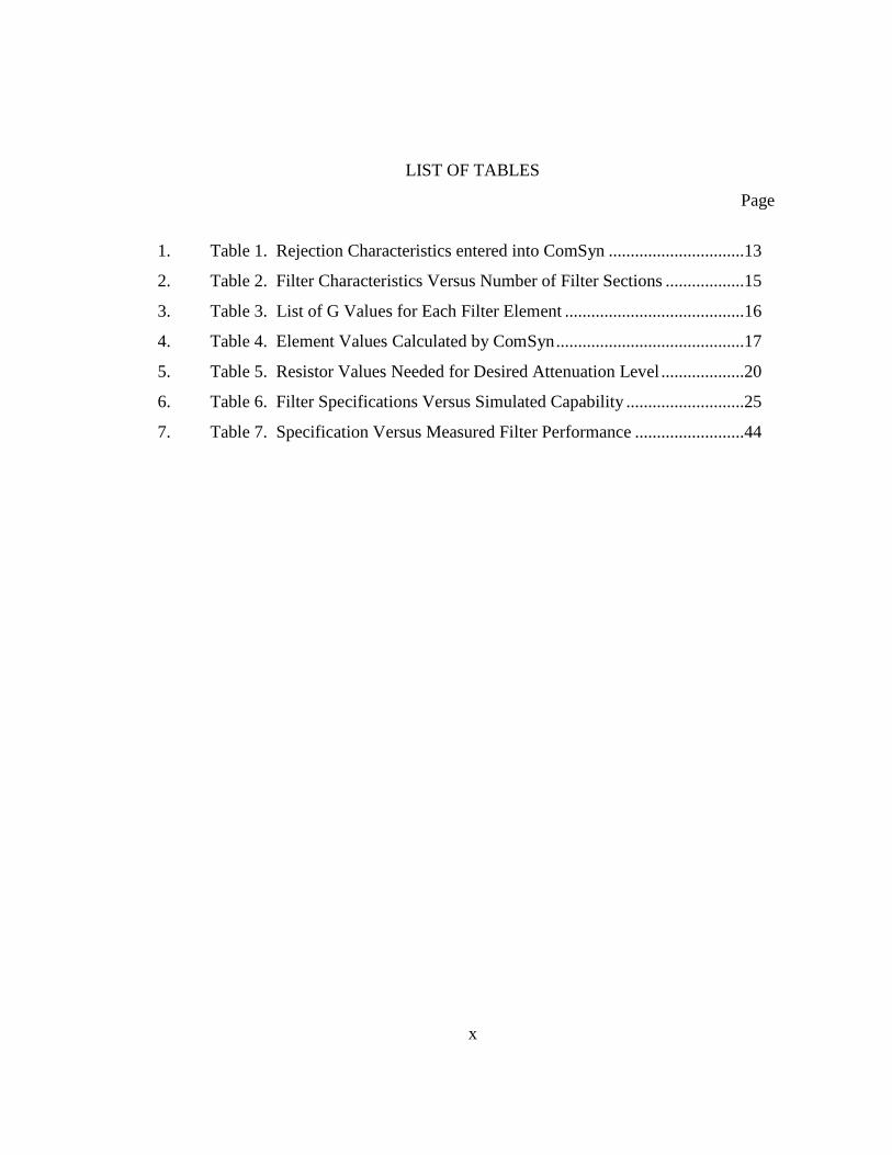
LIST OF TABLES
Page
1. Table 1. Rejection Characteristics entered into ComSyn ...............................13
2. Table 2. Filter Characteristics Versus Number of Filter Sections ..................15
3. Table 3. List of G Values for Each Filter Element .........................................16
4. Table 4. Element Values Calculated by ComSyn ...........................................17
6. Table 6. Filter Specifications Versus Simulated Capability ...........................25
7. Table 7. Specification Versus Measured Filter Performance .........................44
1
Chapter 1
INTRODUCTION
The aim of this project is to design and fabricate a capacitively coupled pi
resonator filter for space flight applications. The specifications of this design are very
stringent; hence a considerable amount of effort has been devoted to meeting the
customer specifications.
1.1 Overview
The design of this filter will take into account a lot of the research that has been
completed in this field. Some of this research is current; however, older research
articles, that have become building blocks for the industry, are also used. The program
used to design the filter, ComSyn, is based on an article written in 1971 by Robert J.
Wenzel [22]. The program was refined using an article written in 1958 by Saal and
Ulbrich [20]. These two articles contain many of the standards used in all passive filter
designs.
The capacitively coupled pi resonator filter structure was selected from a few
different articles, Orchard and Temes’ article [16] and Hajek’s article [9]. The
attenuator – equalizer’s range of capability is analyzed in depth using an article written
by Abromowitz [1]. The overall design, fabrication and performance of passive
networks will be scrutinized [5]. By minimizing parasitic capacitances and modeling
2
them in Touchstone, their effects are minimized using techniques found in Neugebauer’s
article [14].
During the design process, many different aspects of current research were
accounted for. Different filter topologies for passive filters were considered [13] and
passive enhancements to resonator Q [11] were also examined. In the simulation and
realization process of the filter design, optimization of the filter [6] was a very important
factor.
A list of filter specifications including: center frequency, bandwidth, minimum
and maximum pass band insertion loss, maximum pass band variation, maximum pass
band VSWR, minimum rejection requirements, and maximum input power handling
capability were supplied by a customer. The designed filter was constructed within a
housing of a particular size, with connectors at locations specified by the customer. The
type of input/output connectors was also designated in the filter specification.
These specifications were met using a series combination of a band pass filter
and attenuator - equalizer. The band pass filter that was designed is a passive device,
and does not need an external power source to operate, as opposed to an active device
which requires an external power source. This allows much more versatility when
designing a transmission system requiring a filter. [17].”
1.2 Goals of the Project
This project involved the engineering process of designing and fabricating a
band pass filter to meet a list of specifications. The filter was designed within a
3
confined area designated by the specification and consisted of a band pass filter in series
with an attenuator – equalizer. The specification also called out an MSSS (expand the
terms MSSS) connector as its interface, so the filter was designed to use this type of
connector as its input and output. The filter must operate hot and cold temperature
extremes as well as ambient temperature. Every aspect of the dynamic specification was
met by this project; however some details of the design process were omitted due to
proprietary information belonging to Commercial Microwave Technology (CMT).
1.3 Organization of Project Report
The project report is organized as follows: Chapter 2 provides the goals of the
project; what specifications, electrical and physical, will need to be met. Chapter 3 lays
out how these goals will be met and which of the specifications will be the most difficult
to meet. The filter and attenuator – equalizer will be designed as well. Chapter 4 will
summarize the analysis of the by modeling the filter in Touchstone. This simulation will
approximate the filters electrical characteristics. Chapter 5 will discuss how the
theoretical values of the filter components will be realized. The layout of the filter and
attenuator will also be discussed in depth. Chapter 6 includes the analysis of the filter
and the conclusion of the project. The circuit files used in this project can be found in
the Appendix.
4
Chapter 2
CUSTOMER SPECIFICATIONS
2.1 Filter Specifications
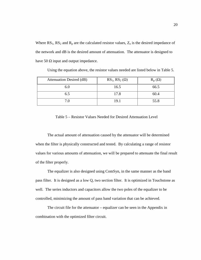
The following chart shows the electrical characteristics the customer desires the
filter to have.
Parameter Specification Center Frequency, fo 900 MHz Minimum -1.5 dB Bandwidth 155 MHz Maximum Low Side -1.5 dB Frequency 829 MHz Minimum High Side -1.5 dB Frequency 970 MHz Pass band for Insertion Loss and VSWR 836 to 964 MHz Maximum Pass band Insertion Loss at Center Frequency
8.0 dB
Minimum Pass band Insertion Loss at Center Frequency
7.0 dB
Maximum Pass band Variation 0.9 dB Maximum Pass band VSWR 1.5:1 (≥ 14.0 dB Return Loss) Minimum Rejection Requirements
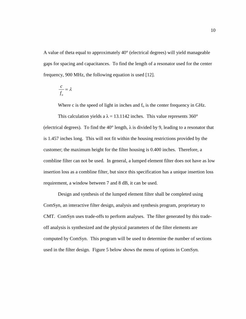
OPTIONS: 1) C: Comsyn - Optimum Combline Filter Design by Z-plane Synthesis. 2) L: Lef - Lumped Element Filter Design. 3) U: Utility - Branches to DOS Shell. - type 'EXIT' to return to program. 4) E: Editor - Provides text editor with Notepad. 5) R: Read data - Reads filter data from a file. 6) S: Save data - Saves filter data to a file. 7) D: cktDir - Opens Circuit File folder with Explorer. 0) X: eXit - Exit this program. > COMSYN -- Press a capitalized letter to make the selection. Press 'ENTER' to select default value shown in <>. Press 'Q' and 'C' to configure default settings.
COMMAND > Comsyn, Lef, eXit. (<C>/L/X):
Figure 5 – ComSyn Main Menu Screen
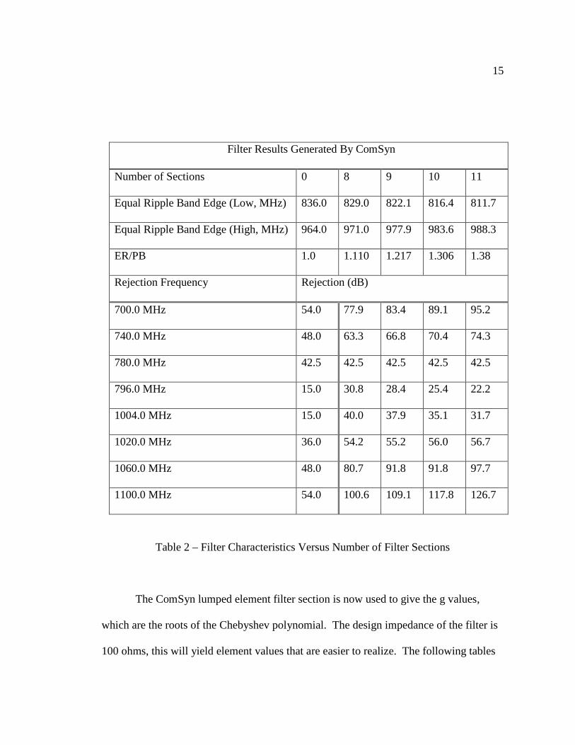
First the combline section of the program will be used to estimate the number of
sections required for the design. This number will then be used by the lumped element
section of the program. The following numbers were entered into the program. Pass
band edges, F1 = 836.0 MHz, F2= 964.0 MHz, Pass band Ripple = 0.02 dB and Theta =
40 degrees. A Chebyshev filter will be designed. It offers steeper roll off on the skirts
of the filter but has more pass band ripples than a Butterworth filter. This ripple will be
designed to be very small, 0.02 db, which will result in a return loss of approximately
21.5 dB or 1.18:1 VSWR. The rejection points were also entered into the program with
12
one variation. The 28 dBc point on the low side was increased by 15 dB. This is due to
the nature of the filters pass band to skew on the low side. In a combline filter, which is
canonically a low pass filter, there is one shunt inductor which causes one of the poles
fall at zero, or DC, and the rest of the poles, (2N-1), fall at infinity. “N” is equal to the
number of sections in the filter. This is what causes the skewing, or flaring, of the low
side of the pass band.
Table 1 shows the design parameters as they were entered into ComSyn. The
rejection values have all been increased by 8 dB, the maximum allowable insertion loss
Figure 10 – Simulated Responses. The three plots are the band pass filter, attenuator – equalizer and series combination. Only the S21 parameters are plotted.
24
4.2 Simulation vs. Specifications
The following table shows the approximate capabilities of the filter simulated by
Touchstone. Actual measurements of the filter will be examined in the conclusion of this
report. The actual measurements will be compared to these simulated values to judge
their accuracy.
25
Parameter Specification Simulation Capability
Center Frequency, fo 900 MHz 900 MHz Minimum -1.5 dB Bandwidth 155 MHz > 155 MHz Maximum Low Side -1.5 dB Frequency
829 MHz 818 MHz
Minimum High Side -1.5 dB Frequency
970 MHz 984 MHz
Pass band for Insertion Loss, and VSWR
836 to 964 MHz 836 to 964 MHz
Maximum Pass band Insertion Loss at Center Frequency
8.0 dB 7.8 dB
Minimum Pass band Insertion Loss at Center Frequency
7.0 dB 7.2 dB
Maximum Pass band Variation
0.9 dB 0.4 dB
Maximum Pass band VSWR 1.5:1 (≥ 14.0 dB Return Loss)
Table 6 – Filter Specifications Versus Simulated Capability
26
As expected, the 28 dBc points are the most difficult parameter to meet.
Although 3 dB should be ample margin to meet the customer’s specification, it is by far
the closest parameter to the specification value. When tuning the filter, these two points
will require the most attention out of all the rejection points. The other parameters are
well within the customer’s specification.
27
Chapter 5
BAND PASS FILTER AND ATTENUATOR – EQUALIZER REALIZATION
5.1 Filter Components
The two main components of the band pass filter that must be realized are
inductors and capacitors. When realizing these components, a very important factor to
take into account is the Q factor. The Q of an element in a filter means a “Higher Q
indicates a lower rate of energy loss relative to the stored energy.” “A high Q tuned
circuit in a radio receiver would be more difficult to tune, but would have more
selectivity; it would do a better job of filtering out signals from other stations that lie
nearby on the spectrum [19].” The physical realization process of the inductors and
capacitors will be discussed at a later point in this chapter.
The band pass filters will be built on steel carriers. The steel carriers will be
mounted to the aluminum housing using 9x 0-80 stainless steel screws. Steel will be used
for the carriers because it’s coefficient of thermal expansion is closer to that of alumina
than the coefficient of aluminum. Aluminum has a thermal expansion coefficient of
approximately 23.0. Steel has a coefficient of approximately 13.0 and Alumina’s
coefficient is approximately 5.4 [7]. Soldering the alumina capacitors to the steel carriers
will not be an issue as long as the overall dimensions of the capacitors are kept below
.200 x .150 inches. If the capacitors were soldered directly onto the aluminum housing,
the dimensional limit of the capacitors would be much smaller. If the capacitor
28
dimensions are too large, the expansion and contraction of the two different types of
materials will cause hair line fractures in the capacitors that would cause the filter to fail.
For this reason, two different types of NTK material [15] are utilized to keep the overall
dimensions of each capacitor within the desired range. A capacitor that is too small
becomes extremely difficult to work with, for this reason the over all dimensions of the
capacitor should be kept above the range of .040 x .030 inches. For capacitance values
that are so low that they fall outside of the desired dimensional range using the lower
dielectric ceramic material (εr = 12.6), double sided copper clad Duroid (εr = 2.2) is used
instead. Duroid is a Teflon based, soft board type material.
The capacitance is calculated using the following equation [11]:
where: C is the capacitance; A is the area of the two plates; εr is the dielectric constant of the material between the plates; ε0 is a constant (ε0 ≈ 8.854×10⁻¹² F m–1); d is the distance between the two plates.
The capacitors in the band pass filter circuit and attenuator are realized using
NTK type A material, a ceramic substrate very similar to alumina, which has a dielectric
constant (εr) of approximately 12.6 and NTK type F material, a ceramic substrate similar
to barium titanate, which has a dielectric constant (εr) of approximately 36.7. This higher
dielectric material is utilized to realize higher capacitance values. The thickness of the
dielectric material used is .010 inches. The material is metalized on both sides using a
29
process known as sputtering. This allows a capacitor to be realized; two metal plates
separated by a dielectric material. The metallization also allows the capacitors to be
soldered on both sides. This high “Q” material allows the filter to be realized closer to
the simulated output and it allows the capacitors to give us an optimal performance for
the housing area allowed.
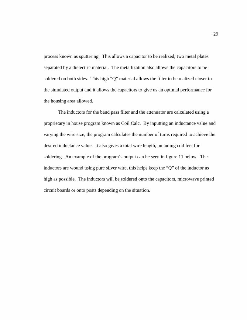
The inductors for the band pass filter and the attenuator are calculated using a
proprietary in house program known as Coil Calc. By inputting an inductance value and
varying the wire size, the program calculates the number of turns required to achieve the
desired inductance value. It also gives a total wire length, including coil feet for
soldering. An example of the program’s output can be seen in figure 11 below. The
inductors are wound using pure silver wire, this helps keep the “Q” of the inductor as
high as possible. The inductors will be soldered onto the capacitors, microwave printed
circuit boards or onto posts depending on the situation.
30
╔════════════════════════════╗ Desc: CH2 L1 ║ SINGLE LAYER AIR CORE COIL ║ C M T Inc. 05-15-2009 -- 18:27:26 ╚════════════════════════════╝ version 080112 ┌──────────────────────────────────────┬───────────────────────────────────────┐ │ INDUCTANCE @ DC ..... 12.05 nH │ INPUT LEG/FOOT .... .025 / .030 inch │ │ │ │ │ No. of TURNS .......... 3.00 turns │ OUTPUT LEG/FOOT ... .025 / .030 inch │ │ │ │ │ INNER DIAMETER ........ .0650 inch │ TOTAL WIRE LENGTH ...... 0.823 inch │ │ │ │ │ WIRE DIAMETER ..# 30... .0100 inch │ COIL BODY LENGTH ........ 0.090 inch │ │ │ TOTAL COIL LENGTH ....... 0.140 inch │ │ SPACING btw'n turns ... .0200 inch │ CAPACITANCE (Cp) ........ 0.071 pF │ │ │ SELF RESONANT FREQ ..... 5454.6 MHz │ │ SHIELD DIA. (.03) .... .272 inch │ INDUCTANCE of LEG ....... 0.51 nH │ ├──────────────────────────────────────┴───────────────────────────────────────┤ │ INDUCTANCE at 900.0 MHz is 12.36 nH, 12.36 nH. Qu = 293 │ ├──────────────────────────────────────────────────────────────────────────────┤ │ For a 3.00 turn coil, the Outer Diameter of the coil is 0.085 inch. │ │ │ │ Use a 0.065 inch diameter Mandrel. Total Wire Length = 0.823 inch. │ │ │ │ INPUT Foot+Leg= 0.055 inch. BODY= 0.090 inch. OUTPUT Foot+Leg= 0.055 inch. │ └──────────────────────────────────────────────────────────────────────────────┘ The Unloaded Q may be inaccurate. (range: .4 < Coil D./Shield D. < .7)
Figure 11 – Inductor Designed by CoilCalc
5.2 Filter Layout
5.2.1 Band Pass Filter Layout
As previously discussed, the filters will be constructed on steel carriers. The
bottom layer of capacitors, or shunt capacitors, will be soldered to the carrier first using
Sn96 solder. The series capacitors, inductors and air capacitors will be soldered to the
shunt capacitors using Sn62. The shunt capacitors have a minimum gap of .020 inches
between one another; this will reduce unwanted parasitic, or stray, capacitances in the
filter. Figures 12 and 13 below show the steel carrier with just the capacitors soldered on.
Figure 13 shows the same carrier in figure 12 but from a different angle. This was
included for clarity and to help the reader visualize the layering of the capacitors. The
31
“+” marks in the first figure are scribed onto the carrier during the fabrication of the part.
They provide the assembler a reference location for each capacitor and will ensure the
Figure 14 shows the completed filter, with the inductors and straps soldered to the
shunt capacitors. This picture was taken from this angle to help the reader understand the
physical layers of the design.
33
Figure 14 – A Few Sections of the Completed Filter
5.2.2 Attenuator - Equalizer Layout
The attenuator section of the filter is realized using a Duroid microwave printed
circuit (MPC) board that is copper clad on one side. The copper is etched off in such a
way to create two 50 ohm lines; one between the end of the filter section and the input of
the attenuator and the other between the output of the attenuator and the output of the
filter housing. A few silver shims have been soldered on top of the 50 ohm lines during
34
the tuning process to improve the filters performance. An additional shim has been
soldered at the junction of the three resistors as well. The MPC board is epoxied to the
steel carrier using a nonconductive structural epoxy. The inductors and capacitors of the
equalizer can be seen in the lower portion of figure 15. The three resistors making the T-
pad attenuator can be easily distinguished as well.
Figure 15 – Attenuator - Equalizer
35
The input to the band pass filter section is also realized using a Duroid MPC
board that is copper clad on one side. It is also etched in the same manner as the
attenuator MPC board to create a 50 ohm line between the input feed through and the
input of the filter section.
5.2.3 Housing Arrangement
Feed throughs will be utilized to create coaxial input and output ports at the
customer specified locations. The feed through consists of a center conductor encased in
glass and a Kovar ring which is fired. The center conductor is realized by a Kovar pin
that is plated with a thin layer of electroplate nickel and a more conductive gold layer.
The outer Kovar feral ring is also plated with nickel and gold. In order to connect the
inside feed through pin to the input and output MPC boards, a small brass feed through
bushing is soldered on to the feed through pin. This allows a .003 silver ribbon to be
soldered to connect the two together.
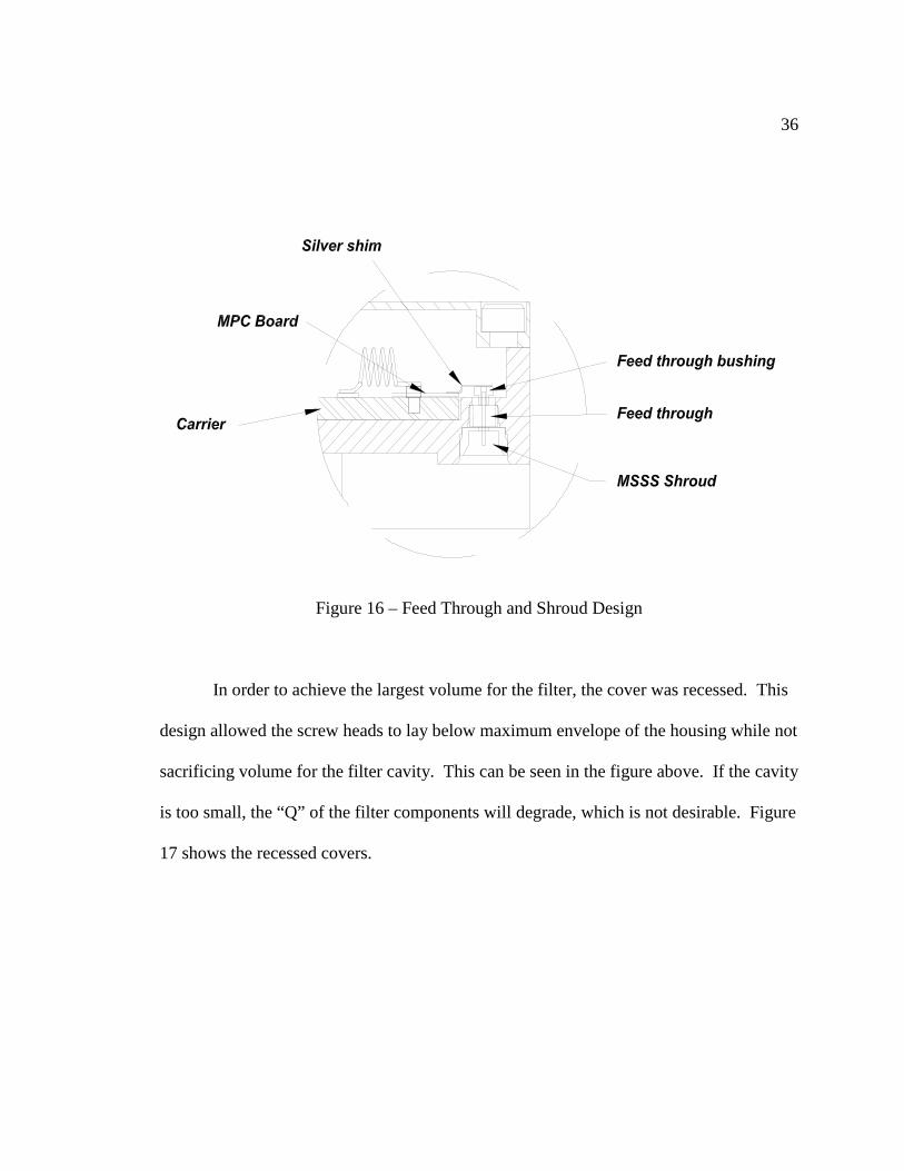
The customer specification requires the use of MSSS connectors at both
interfaces. An MSSS shroud will be held in the housing with a press fit. The interface of
the MSSS shroud and feed through will be inspected for concentricity; it must be
concentric for it to properly accept an MSSS cable or bullet. Figure 16 shows the
arrangement of the MSSS shroud, feed through and feed through bushing. It also helps
demonstrate how the components are arranged in the housing.
36
Figure 16 – Feed Through and Shroud Design
In order to achieve the largest volume for the filter, the cover was recessed. This
design allowed the screw heads to lay below maximum envelope of the housing while not
sacrificing volume for the filter cavity. This can be seen in the figure above. If the cavity
is too small, the “Q” of the filter components will degrade, which is not desirable. Figure
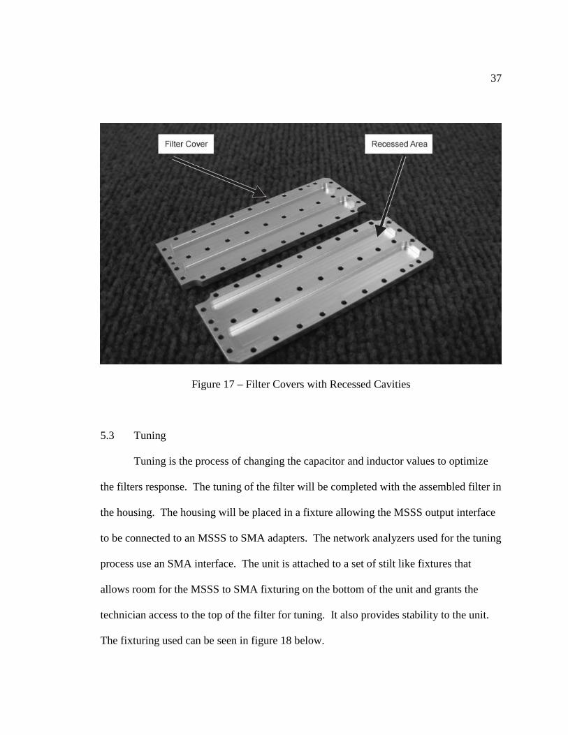
17 shows the recessed covers.
37
Figure 17 – Filter Covers with Recessed Cavities
5.3 Tuning
Tuning is the process of changing the capacitor and inductor values to optimize
the filters response. The tuning of the filter will be completed with the assembled filter in
the housing. The housing will be placed in a fixture allowing the MSSS output interface
to be connected to an MSSS to SMA adapters. The network analyzers used for the tuning
process use an SMA interface. The unit is attached to a set of stilt like fixtures that
allows room for the MSSS to SMA fixturing on the bottom of the unit and grants the
technician access to the top of the filter for tuning. It also provides stability to the unit.
The fixturing used can be seen in figure 18 below.
38
Figure 18 – Fixturing used for Tuning Process
The inductor values will be tuned by adjusting the spacing between the turns. The
spacing between the inductor and the ground plane is important to setting its inductance
value. In extreme cases, the inductors can be rewound with a smaller or larger inner
diameter to adjust the inductance.
The capacitors will be tuned by trimming the metallization on the top surface with
a diamond scribe or by soldering a .003 inch thick silver shim on top of the capacitor.
When a shim is added, the amount of metal hanging over the edge of the capacitor creates
39
an air capacitor to add capacitance to the component. Most of the series capacitors in the
circuit are designed to have a tunable air capacitor next to the fixed series capacitor.
Figure 19 is a diagram of the air capacitor and it can be seen below. The air capacitor is
made by soldering a .003 inch thick silver shim on one end and leaving the other end
hanging above the next shunt capacitor. By increasing and decreasing the distance
between this air capacitor and the shunt capacitor, the capacitance is changed, allowing
the series capacitance to be tuned. The dimensions in the figure below are in inches.
Figure 19 – Air Capacitor used for Tuning Process
By trimming the metal on the top surface of the capacitor with a diamond scribe,
the surface area of the parallel plate capacitor is lowered, therefore decreasing its
capacitive value.
The filter will be tuned well within the customer’s specifications. The two
specification points that will be the toughest to meet are the two 28 dBc points. As a
goal, the filter will be tuned to at least 31 dBc at those two frequencies. The initial tuning
40
process will focus on the 28 dBc points in the specification and the pass band VSWR.
The series resistors in the attenuator will be replaced with silver shims to simulate a 50
ohm line. After the filter tuning is complete, the silver shims are removed and the
resistors are soldered in. Minimal tuning will be needed in the filter at this point, and
most of the tuning will be done in the attenuator/equalizer section. It is very difficult to
tune the filter with the equalizer/attenuator properly installed. The resistors mask the
filter’s response and it becomes difficult to decipher what exactly is happening while
tuning.
41
Chapter 6
FINAL PERFORMANCE OF THE 836 – 964 MHz BAND PASS FILTER AND ATTENUATOR - EQUALIZER
6.1 Analysis & Conclusion of Measured Data
The following figures are plots are data from a network analyzer characterizing
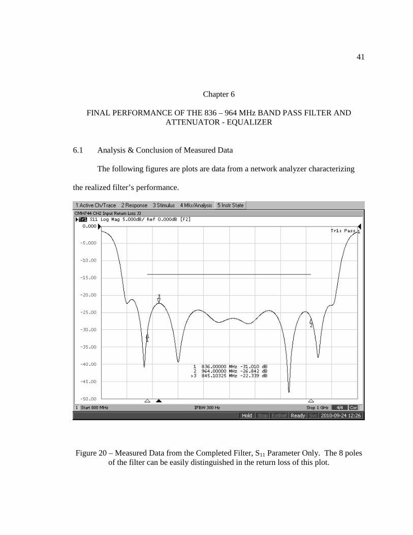
the realized filter’s performance.
Figure 20 – Measured Data from the Completed Filter, S11 Parameter Only. The 8 poles of the filter can be easily distinguished in the return loss of this plot.
42
Figure 21 - Measured Data from the Completed Filter, 1.5 dBc Bandwidth, S21 Parameter Only.
43
Figure 22 - Measured Data from the Completed Filter, Pass Band Variation, S21 Parameter Only.
44
Figure 23 - Measured Data from the Completed Filter, Rejection Performance, S21 Parameter Only. Markers are referenced to the center frequency marker.
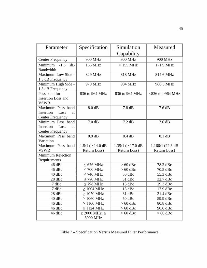
Table 7 compares the capability of the simulation to the actual measured numbers
of the realized filter. This will allow the quality of the simulation to be assessed and
where we can expect to have issues with future designs. Ideally, the measured values
would exceed the simulation’s expected values. This would allow for greater confidence
in how the realized filter will perform if the simulation meets the given specifications.
45
Table 7 – Specification Versus Measured Filter Performance.
Parameter Specification Simulation Capability
Measured
Center Frequency 900 MHz 900 MHz 900 MHz Minimum -1.5 dB Bandwidth
155 MHz > 155 MHz 171.9 MHz
Maximum Low Side -1.5 dB Frequency
829 MHz 818 MHz 814.6 MHz
Minimum High Side -1.5 dB Frequency
970 MHz 984 MHz 986.5 MHz
Pass band for Insertion Loss and VSWR
836 to 964 MHz 836 to 964 MHz <836 to >964 MHz
Maximum Pass band Insertion Loss at Center Frequency
8.0 dB 7.8 dB 7.6 dB
Minimum Pass band Insertion Loss at Center Frequency