Industrial Technology Electronics HSC 2001 – ACLC Folio DESIGN Statement of Intent Research Development of Concepts & Ideas Selection & Justification of Materials, Components, Process & other Resources - Materials - Components - Processes - Other Resources MANAGEMENT Timeline Finance Plan Use of Appropriate Industrial Processes & Equipment Evidence of Safe Working Practice & OH&S Issues WORKPLACE COMMUNICATION Workshop Drawings Record of Procedures Sketches Calculations PROJECT EVALUATION Evidence of Ongoing Evaluation Appropriateness of Design and Design Modifications Student’s Evaluation of the Major Project and its Relationship to Statement of Intent PRODUCTION Quality of Product Evidence of a Range of Skills Degree of Difficulty Links Between Planning and Production Evidence of Industrial Processes Use of Appropriate Materials Use of Industrial Technologies Evidence of Problem Solving Appendices Appendix 1 - The OH&S Act. Appendix 2 - Letter From Licenced Electrician. Appendix 3 - Overlays of Circuit Designs. Appendix 4 - Business cards of people that I consulted or procured components from. Appendix 5 - New method of producing PCB’s. Appendix 6 - Computer Program. Appendix 7 - Diary
DESIGN Statement of Intent Research Development of Concepts & Ideas Selection & Justification of Materials, Components, Process & other Resources - Materials - Components - Processes - Other Resources
MANAGEMENT
Timeline Finance Plan Use of Appropriate Industrial Processes & Equipment Evidence of Safe Working Practice & OH&S Issues
WORKPLACE COMMUNICATION
Workshop Drawings Record of Procedures Sketches Calculations
PROJECT EVALUATION
Evidence of Ongoing Evaluation Appropriateness of Design and Design Modifications Student’s Evaluation of the Major Project and its Relationship to Statement of Intent
PRODUCTION
Quality of Product Evidence of a Range of Skills Degree of Difficulty Links Between Planning and Production Evidence of Industrial Processes Use of Appropriate Materials Use of Industrial Technologies Evidence of Problem Solving
Appendices Appendix 1 - The OH&S Act. Appendix 2 - Letter From Licenced Electrician. Appendix 3 - Overlays of Circuit Designs.
Appendix 4 - Business cards of people that I consulted or procured components from.
Appendix 5 - New method of producing PCB’s. Appendix 6 - Computer Program.
Statement of Intent This year for my Industrial Technology major practical project I intend to design and build a Switching Device that automatically turns lights and other electrical equipment on and off at predetermined time. What the Project is • Basically its a 240 VAC automatic timer • The project will use some sort of computer controlled timer circuit which will
be able to switch 240 VAC on and off. The time intervals will be predetermined using a computer program. The program should be written in stamp basic so the program can be changed easily.
Motivation & Purpose of the Project Motivation • The main motivation was due to the increasing number of break-ins in my
neighbourhood, so when we go on holidays or away for the weekend we often leave the light on in the living room so at night it looks like someone is home.
Purpose
• The Purpose of the project will be for when we go away we can plug in
some lights on extension cords and run them into separate rooms and then set the program in the project to turn on light at curtain times and also turn them off again. The theory behind this is that it will look like someone is walking from room to room turning the light on, staying for a while, and then leaves turning the light off and going to another room. Also to be able to operate a TV or HiFi giving added effect that someone is home
Parameters of the Design The Design should allow the project to:
• Fit into a case about 500mm (width) x 100mm (height) x 400mm (depth • Have a minimum of 8 outputs for 240 VAC • Easily programmable by computer • Have a high-tech, modern appearance, so it blends in with the house
What are the Possibilities ? Some Possibilities that have to be looked into at these early stages are:
• What is the case going to look like? • What type of 240 VAC outlet will be used? • What type of circuits will be used?
• What regulations, given the use of 240 V controller devices?
• How will it all be powered • How will it be programmed
Uses for other Applications
• At present there is no other anticipated uses for the project, but it would be possible for any 240 VAC appliance to be used on the circuit.
Research I asked myself the following questions and the made it my mission to find the answers:
• Are there any similar products out on the marker?
Yes there are, but they don’t do what I want. All the 240 volt timers on the market only have one output and one timer.
• How would I switch 240 VAC using only a low DC Signal?
After consulting with 2 electricians, is was obvious the a relay should be used to switch the 240 VAC.
• What type of circuitry will be required?
What was needed was a circuit that could be pre-programmed by computer, and then left to follow its program with no connection to the computer. The solution was found one day looking through the Dick Smith Electronics catalogue when I came across a small circuit called a “Basic Stamp 1 Revision D”. Thinking back, knowing that I had heard of a “stamp” circuit before. I remembered that the stamp Chip is the main part of a robot that students make and race in a electronics competition called a “Bilby comp”, which I had taken part in 2-3 years ago. Going back over my designs I found the robot circuit, and that is where the experiments began.
Experiment 1 Aim: To design a prototype controller unit using the stamp chip
controller circuit from the robot circuit.
Method: With the help of past diagrams of the robot circuit, and the help of a friend who had used the stamp 1 chip before, I was able to go about making modifications to the circuitry using a C.R.O and multimeter to determine what the components were doing. With this knowledge, modifications were possible.
C.R.O Multimeter Result: I was able to determine what each of the components did, and
there for was able to get rid of a lot of useless components and add what I needed.
Conclusion: The prototype was a success and was a great place to start. Experiment 2 Aim: How could a relay be connected to the controller board? Method: A number of sketches where used to illustrate how the circuit
would work. The experiment used a number of different set-ups expressed on the computer in graphical format so that modifications were easily done. The use of extra new components was also implemented.
MS Paint was the chosen program for the design prosess as it is easy to use and simple to creat component symbols.
Many boards such as this were created.
Result: After a number of weeks of design after design a portable
isolated relay board design that incorporated an opto-isolator was designed and used in the final development.
Conclusion: Since the experimental relay board was exactly what I wanted,
the only modification that was made to it for the final design was that it was reduced in size to make it more compact.
Experiment 3 Aim: the testing of a new PCB creation process. Method:
The following steps where followed: • Designing of the overlay circuit on computer. • Printing onto special glue coated paper using a laser printer. • Placing the paper face down on a copper board, and applying
heat from an iron for 3 minutes. • Soaking in water till the paper floated off leaving a toner
protection layer which would prevent etching of the tracks. Result: The test was not successful, as the tracks did not properly stick
to the copper when heating. This was partially fixed by applying more heat. But it still wasn’t up to standard as the toner came off in the etching solution.
Conclusion: this method was not as good as the old method that I had been
currently using, where a Dailo pen was use, or copying the circuit onto a clear plastic overlay and copying onto a negative photo-resist board.
Experiment 4
Aim: The testing of Positive photo-resist board instead of Negative photo-resist board.
Method: the method of creating a positive photo-resist board is very
similar to creating a negative photo-resist board, but instead of using a black background with clear tracks of plastic to let UV light react with the photo-resist board to create tracks, Positive photo-resist board uses black tracks on clear plastic under UV light to create tracks on the board.
Positive Photo-resist overlay Negative Photo-resist overlay Method of proses:
• Design circuit on computer. • Print onto plastic sheet. • Cut a piece of positive photo-resist board to size. • Put in UV light box for 80 seconds with overlay on top. • Keep in the dark for 5 minutes. • Develop using positive resist developer. • Drill hole where components need to go. • Etch. • Clean with mineral turpentine. • Resin coat and leave to dry.
Results: The process worked perfectly first time without and mistakes. Conclusion: The Positive photo-resist way might be even easier then the
negative photo-resist way. It is defiantly better as on mistakes were made on the board.
Development of Concepts & Ideas
Development of ideas about, how the relay would be connected to the stamp controller unit.
OPTIONS CHOICE JUSTIFICATION OF CHOICE Main case: Plastic Case Zippy Box Steel Enclosure Relay Case: Zippy Box Plastic Case Steel Enclosure PCB’s: Copper Board Silver Board
Plastic Case Zippy Box Copper Board
Is inexpensive, Easy to drill holes, and easy to attach items inside the large case area. Small, inexpensive, and durable. Inexpensive and radially available.
- Components
OPTIONS CHOICE JUSTIFICATION OF CHOICE ELECTRONICS Resistors: Carbon film Metal film wirewound Capacitors: Electrolytic Metallised poly Polyester Ceramic LED’s: Standard 5mm Standard 3mm LED bar graph Transistors: Relay- BD139 - BD140 Switches: SPDT illuminated Soft Touch SPDT Miniature DPDT 3A 250V Transformers: 0-12-15-18V@1A 12-0-12 @ 0.15A 12.6 CT @ 0.5A CONNECTIONS: Computer to unit: 6.5mm stereo plug
Carbon Film Electrolytic Metallised Standard 5mm BD139 SPDT illuminated soft touch 0-12-15-18 @ 1A 6.5mm stereo
Readily available, inexpensive & I already had a few of them. Inexpensive, reliable, Compact, & easy to work with. Inexpensive, Small, but big enough to work with. Only one available. Looked good and lit up when it was on. Most powerful 12v transformer, without costing too much. Simple to use, strong, only one way it can be connected to stop confusion.
3 pin DIN plugs Unit to relay: RCA Plugs 2 pin DIN 4 pin DIN 240v from relay: Extension Lead Power board 4 way power point 2 way power point single power point
RCA plugs Extension Lead
Easy to connect, & replacement cables are available. Inexpensive.
- Processes & Other Resources OPTIONS CHOICE JUSTIFICATION OF CHOICE Making the PCB’s Positive Photo-resist Board. Negative Photo-resist Board. Copper board & Dailo Pen. Toner Track (see Experiment 3).
All were used, but Positive Photo-resist was preferred.
Was easier to use than the other ways. The tracks always copied without error.
12VDC illuminating SPST 240VAC switch P 7586 1 $12.48 $12.48 6.5mm stereo DPST socket P 1296 1 $2.00 $2.00 6.5mm stereo pro gold plug PP0177 1 $4.45 $4.45 RCA socket 1x2 on phenolic PS0263 2 $0.90 $1.80 RCA socket 2x3 on phenolic PS0268 2 $2.55 $5.10 RCA plug plastic red PP0240 9 $0.56 $5.04 RCA plug plastic white PP0244 9 $0.56 $5.04 IEC power lead PS4106 1 $8.50 $8.50 IEC 320 male chassis PP4005 1 $2.95 $2.95 25 pin sub D plug solder tail connector P 2690 1 $3.18 $3.18 25 pin sub D plastic shell P 2692 1 $3.18 $3.18 Main case total $69.68 Test Components & PCB $25.00 Miscellaneous & wire & solder $15.00 Project Total $192.80
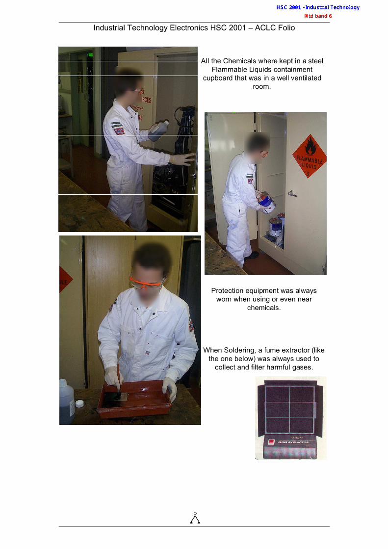
Use of Appropriate Industrial Processes & Equipment Industrial Equipment & Processes to manufacture “ACLC” included:
• Photo-resist coated Boards, used in conjunction with laser printer, printable flim. Is a widely used method in industry were a small to medium number of boards are required. The Photo-resist board is exposed to UV light, in a light box, and reacts were the tracks were or weren’t, depending on if it was positive or negative resist board. The board is then developed in positive or negative developer, and then etched in an Ammonium Persulfate solution.
• Other Industrial Equipment used included:
Fixed Bench Drill Gelatine Disk Sander Soldering Iron Fume Extractor Etching Tank
• Chemicals used:
Ammonium Persulfate Mineral Turpentine Resin Positive or Negative Developer
Record of Procedures Most of the time in the early stages was taken up with research and designing either on the computer and the internet, or the old fashion way of pen, paper, and books. During this stage, many professional and experienced people in the electrical and electronics industries where consulted with so that I could get many opinions and make a more informed decision on how to design and make my project, “ACLC”. A selection of Business card of people that I consulted or bought components off is located at the back of the folio under (Appendix 4). Knowing what I wanted to make, I proceeded to investigate into the use of circuits that could be pre-programmed by computer, and then left to follow its program with no connection to the computer. The solution was found one day looking through the Dick Smith Electronics catalogue when I came across a small circuit called a “Basic Stamp 1 Revision D” (see picture 1). Thinking back, knowing that I had herd of a “stamp” circuit before, I remembered that the stamp Chip is the main part of a robot that students make and race in a electronics competition called a “Bilby comp”, which I had taken part in 2-3 years ago. Going back over my designs I found the robot circuit (see diagram 1), and that is where the experimental designing began.
The first design consisted of the controller section of the bilby circuit and a relay connected to each output with a common 240 volt active track. This proved impossible to implement as the relays that could switch 240 volts required 12 volts to run the coil, and the outputs of the stamp chip was only 5 volts. (see diagram 2).
Diagram 2
After trying to come up with an idea on how to run a 12 volt relay of 5 volts, a friend in the electronics class told me about a small micro chip looking device, called an optocoupler. It’s made up of a led and a photo-transistor an a plastic box, similar size to a NE555. The optocoupler uses a small voltage to turn on a LED that then activates the photo-transistor in the other circuit. (see diagram 3)
Diagram 3 The good thing about the optocoupler was that it isolated the 5 volt controller board from the 240 volt relay circuit so there was no connection at all. Although the optocoupler was a great idea, a 12 volt circuit still had to be designed so that the relay could work. A diagram of the circuit with the optocoupler is shown in (diagram 4).
The idea to connect all the boards was one that I had had since the start, so a transformer circuit with both 12 v and 5 v outputs was designed. The transformer circuit was similar to the demonstration circuit in a Dick Smith catalogue, (see diagram 5), but my circuit had instead of one voltage regulator, had two. One for 12 volts and the second for 5 volts. The design could then ran a 12 volt track along the top of the board for the relays to get power off, (see diagram 6) and still power the controller board.
Diagram 5
Diagram 6
Deciding that the board was just too big I decided to make all the boards separately and connect the boards with wire. This is where the idea for 8
separate, mobile relay board originated. This meant that the relay boards could be placed in any room of the house. (see figure 1)
Figure 1
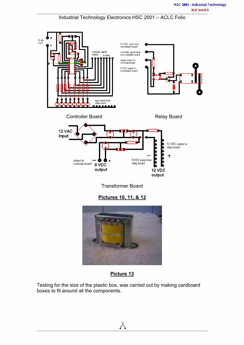
When I finished designing the 3 circuit board, (the transformer, controller, and relay boards), I then connected the boards on paper the way they would appear in real life, (see diagram 7) and when over it with my electronics teacher, Mr Baguley. With use not finding any noticeable problems with the circuitry, I then proceeded to have the circuit checked with a licenced electrician to make certain that it would work and that it complied to safety regulations.
The first problem occurred when transferring the circuit design from the computer to the plastic overlay. When I printed out the overlay and sized it up with the stamp chip I found that the overlay was far to big and had to be re-printed at a smaller size. Before re-printing the circuit overlay, I decided to try a new method of producing PCB’s (see appendix 5), which consisted of using a laser printer, and printing on special paper that would transfer the toner tracks to the copper board when heat was applied to the paper and board by a iron. (see picture 2). With the paper stuck to the copper board, it is placed into a container of water till the paper floats off, leaving the track. (see picture 3). The did not happen all the times that I tried this method, so this method was not adopted. A sample of the paper with a copy of the relay board is located below.
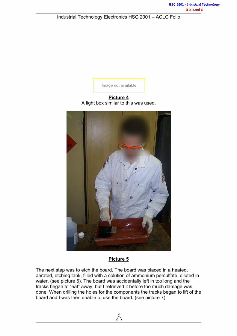
I printed out the overlays (see appendix 3) at the right size and proceeded to cut to sizes a piece of negative resist board for the controller circuit. The negative photo-resist board was placed in a UV light box (see picture 4) with the photo-resist surface (covered by the black background “negative” overlay) facing the UV lights. Exposed to the light for 45 seconds and then kept it the dark for 5 minutes caused the board to reacted to where the UV light had touched the board, leaving tracks when the board was developed, using a negative resist developer chemical. (see picture 5).
The next step was to etch the board. The board was placed in a heated, aerated, etching tank, filled with a solution of ammonium persulfate, diluted in water, (see picture 6). The board was accidentally left in too long and the tracks began to “eat” away, but I retrieved it before too much damage was done. When drilling the holes for the components the tracks began to lift of the board and I was then unable to use the board. (see picture 7)
The same process was used to make the relay board, but before etching the holes for the components were drilled so that the tracks wouldn’t rip off the board. The board was then etched and finished up ok.
A new method was used for the Transformer Board that I came up with. First I printed out the circuit design on paper, in reverse on a laser printer. Then placed face down on a pre-cut to sizes copper circuit board, and heated using an iron for 3 minutes. The result was a toner track on the copper board. I then
went over the tracks (see picture 8) with a dailo pen (see picture 9) to stop the tracks from dissolving off. The holes for the components were then drilled and the board was then put in the etching tank. When etched, I attacked the board with steel wool to clean the copper tracks and the resin coated them to make for easier soldering.
Picture 8
Picture 9 Next step was to make the controller board which was made using negative photo-resist board, in the same method as the Relay board. When all three board where made I went and bought the rest of the components for the boards and then soldered them into their correct places (see pictures 10, 11, & 12). A problem that occurred was that the holes in the transformer board where too far apart and had to be re-drilled and links attached so the components could work. But a part from that, it went together pretty good. Also, a transformer was bought to connect to the transformer board. (see picture 13)
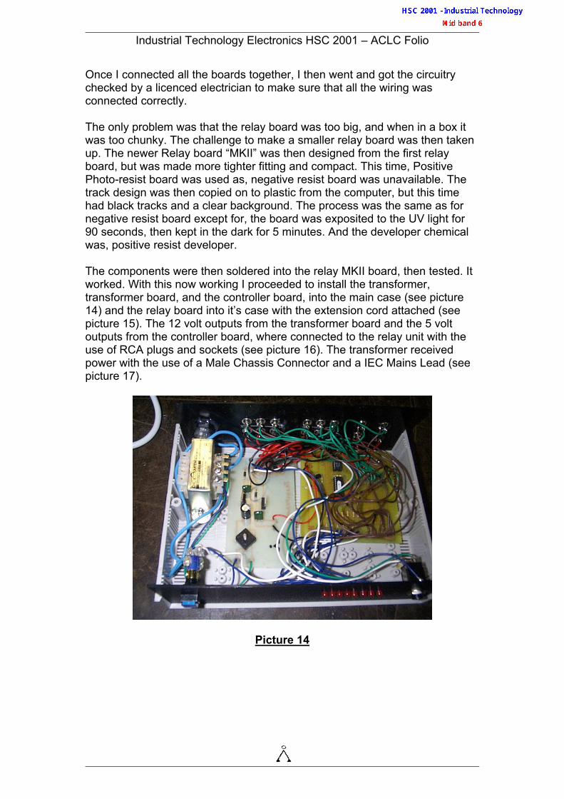
Once I connected all the boards together, I then went and got the circuitry checked by a licenced electrician to make sure that all the wiring was connected correctly. The only problem was that the relay board was too big, and when in a box it was too chunky. The challenge to make a smaller relay board was then taken up. The newer Relay board “MKII” was then designed from the first relay board, but was made more tighter fitting and compact. This time, Positive Photo-resist board was used as, negative resist board was unavailable. The track design was then copied on to plastic from the computer, but this time had black tracks and a clear background. The process was the same as for negative resist board except for, the board was exposited to the UV light for 90 seconds, then kept in the dark for 5 minutes. And the developer chemical was, positive resist developer. The components were then soldered into the relay MKII board, then tested. It worked. With this now working I proceeded to install the transformer, transformer board, and the controller board, into the main case (see picture 14) and the relay board into it’s case with the extension cord attached (see picture 15). The 12 volt outputs from the transformer board and the 5 volt outputs from the controller board, where connected to the relay unit with the use of RCA plugs and sockets (see picture 16). The transformer received power with the use of a Male Chassis Connector and a IEC Mains Lead (see picture 17).
Now came the time to upload a program to the stamp chip. This did not happen. Thinking that the cable was incorrectly wired, I checked the continuity in the connections with a multimeter and then followed the connections down from the computer parallel output to the circuit board without finding an error. I then started to check the board for gaps in the track. Looking at my plan for the circuitry I found that a few pins of the memory chip where not connected to all the tracks they where suppose to be connected to. Linking up these gaps with copper wire and solder I then tried to upload the program again. This was done without success. Getting frustrated at it, so I left it and went to bed. The next morning I got up to continue finding the problem but when I switched it on it uploaded first time. This was the result of the stamp chip getting too hot and shutting down. All that was required was time to let it cool down. Stamp chip (see picture 18).
Picture 18 With the entire project working, I then went to get it Checked and approved by a Licenced Electrician. He found it to be “assembled and wired in a correct manner and safe for operational use” (see Appendix 2). The last thing to do was to write a program to test the unit (see Appendix 6). Two programs where written, one using long intervals between switching, such as 15 - 30 minute intervals. And one with short intervals such as 15 - 30 second intervals. The finished Product (see pictures 19).
• The first few months consisted of research and design ideas where I was constantly evaluating the ideas, designs, and processes. Many design attempts were made to get the final result of an extremely good circuit.
• Due to the lack of availability some parts, other parts where chosen to do the same job, such as the transistor for the relay board, the BD140, was replaced with a BD139.
• The use of different boards was because I was constantly testing the reliability of different method and procedures.
• Relay board “MKII” was the result of the need to make the circuits smaller. That was achieved by reducing the surface area of the circuit by over 70%.
Appropriateness of Design and Design Modifications The Final design wasn’t perfect, but it was close! It was appropriate because: - the final design does exactly what I said it would do in the
statement of intent. - It’s smaller and more mobile than was originally planned. - Circuity modified, is a lot smaller in size then the original circuity. - Easy to mass produce - Use of Positive Photo-Resist board, made for easy, and accurate,
Manufacture of PCB’s. It wasn’t appropriate because: - during the modification process, some links were forgotten, causing
later problems. - The design was still able to be reduced in size and made to look
better, more “Hi Tec”, but the cost would have been too much.
Student’s Evaluation of the Major Project and its Relationship to Statement of Intent Intentions of the Project: • The project will use some sort of computer controlled timer circuit, which
will be able to switch 240 VAC on and off. • The time intervals will be predetermined using a computer program. • The program should be written in stamp basic so the program can be
changed easily. • Fit into a case about 500mm (width) x 100mm (height) x 400mm (depth). • Have a minimum of 8 outputs for 240 VAC.
• Have a high-tech, modern appearance, so it blends in with the house.
• The Quality of the finished product reflects the amount of time, effort, and hard work that was extended to the best of my ability on the project “ACLC”.
• The quality is represented by mainly in the circuitry used in the units,
and it’s ability to handle 240 volt current, up to 10 amps (2400 watts).
• The case design expresses the modern looks, of today’s products, which people associate with quality.
• This project has been examined by a Licenced Electrician, and been
proven to comply to all safety regulations. (See appendix 2). Evidence of a Range of Skills The range of skills used in this project included:
• Sketching of ideas. • Drawing of designs. • Knowledge of computer drawing programmes. • Knowledge of both, negative & positive UV photo-resist boards. • Understanding of Ammonium Persulfate, for Etching copper PCB
boards. • Soldering Skills. • Able to program in Stamp Basic (.bas format). • Problem solving skills. • Calculations of component Values.
Degree of Difficulty The Degree of difficulty was demonstrated by:
• The use of positive & negative UV photo-resist boards, in the transfer of the circuit onto copper boards.
• The use of complex components in the circuit, such as the Optocouple,
Stamp chip, timer, and memory chip.
• Use of a UV light box to transfer track designs from a plastic overlay, to the photo-resist board.
• Writing a program in Stamp Basic, to control the Units. • Management of funds and equipment.
• Research took up a big part of my time in the early days of the project, but the research was used to start my experiments and test on what components would be right for the job, and what methods of production would work.
• Even though the tests had been done at the start, I found it necessary
to refer back to my original research and conduct small tests during production.
• Close reference to the timeline, helped me to keep on track of time and
not fall too far behind. • Early designs and sketches were used to design the final Printed
Circuit Boards. Evidence of Industrial Processes Observing all OH&S Regulations, the following Industrial processes were used in the construction of “ACLC”.
• Use of a UV light box to transfer tracks onto Photo-resist boards, and then using positive or negative developer to display the tracks for etching.
• Etching using Ammonium Persulfate, diluted in water, and in a heated,
Aerated tank, to Etch the copper of the Printed Circuit Boards.
• Soldering using 5 core resin filled, 60/40 tin/lead, 1.25mm solder. This was my choice of solder as not much solder is required to solder in components, and it can be used in bulk with wires and connections.
• All boards were cut to size using a guillotine and then shaped using a
disk sander. Use of Appropriate Materials The selected materials used in the production were appropriate because:
• The plastic cases insulates the circuits so, if somehow a wire came loose the case would not become live, as it would if it was a metal case.
• The use of copper boards as it is a good conductor, and heat
dissipation properties. • All the components turned out to be appropriate for the job, as all the
components are never under much, or at times “no” Load, meaning that the components will last longer than their expected life span.
Use of Industrial Technologies Industrial technologies were used:
• Computers played a big part in the production the project “ACLC”, as they were used all the way throught the project
• In the research process, with the use of Industrial Catalogues, CD’s and web sites.
• Planning was also conducted by consulting people in the industry. • In the construction of working drawings with the use of Computer Aided
Drawing Programs (CAD).
Evidence of Problem Solving Problems in counted during the production of the “ACLC” were:
• The track designs wouldn’t print at the right size. • The tracks were copied onto a Copper board around the wrong way. • The copper tracks came of when drilling the holes. • The components didn’t fit into the holes in the PCB’s. • The program wouldn’t up load to the stamp chip.
Solutions:
• To get the right track size on the print outs, a number of trial and error prints were carried out till the right size was achieved.
• The only way to solve this problem was to either solder the
components onto the copper side of the board or create a new board, so a new board was created.
• To get around the problem of the tracks coming off when drilling the
hole after etching, the idea of drilling the hole before etching when the whole board is copper, was implemented and proved to work.
• Since the components didn’t fit into the holes that were predrilled in the boards before they were etched, new holes had to be drilled with links from the components to where the should have been. Thinking that the cable was incorrectly wired, I checked the continuity in the connections with a multimeter and then followed the connections down from the computer parallel output to the circuit board without finding an error. I then started to check the board for gaps in the track. Looking at my plan for the circuitry I found that a few pins of the memory chip where not connected to all the tracks they where supposed to be connected to. Linking up these gaps with copper wire and solder I then tried to upload the program again. This was done without success. Getting frustrated at it, so I left it and went to bed. The next morning I got up to continue finding the problem but when I switched it on it uploaded fist time. This was the result of the stamp chip getting too hot and shutting down.
All that was required was time to let it cool down.
The end result was a device that could be programmed by computer in Basic Stamp and left independent to switch on and of relays which controlled 240 volt AC.


![Statement of intent [autosaved]](https://static.documents.pub/doc/80x56/55544affb4c905b7428b4bfe/statement-of-intent-autosaved-5584a0674cf41.jpg)


