ISSN: 2278 – 909X International Journal of Advanced Research in Electronics and Communication Engineering (IJARECE)
Volume 5, Issue 2, February 2016
285
All Rights Reserved © 2016 IJARECE
DESIGN VERIFICATION OF POWER MANAGEMENT UNIT
AND CLOCK GENERATION BLOCK OF Wi-Fi SoC
Abstract
It is all about the importance of
the system on chip and the typical
intellectual property design verification
flow that is followed in the industry,
motivation behind this project and the
time plan that was followed in the
execution of project.
The term “system on a chip”, or
SOC really implies two things, the
product itself and the methodology used
to design it. A SOC product integrates
several sub-systems, many or all of
which would’ve been separate discrete
chips in the past into a single chip.
Depending on how tightly you restrict
the definition, a SOC may be only a
single silicon die, or possibly many dies
inside a single package. Either way, a
SOC is rarely the entire system on that
single chip, but it usually encompasses
the computing functions of the device.
Index Terms : System on
chip(SOC),Silicon die.
Introduction
System On a Chip (SOC) is an
implementation technology and may have
many transformations and many different
variants during this execution flow. A
typical SOC may contains the cores like a
processor or processor sub-system, a
processor bus, a peripheral bus, a bridge
between the two buses, and many
peripheral devices such as data
transformation engines, data ports (e.g.
UARTs, MACs) and controllers (e.g.,
DMA). The sub-systems included in a
specific SOC depend on the intended
device and a series of tradeoffs and
requirements, such as cost, form factor,
power, performance, and functionality.
The verification methodology of an
SOC flow includes the stimulation of
design by providing input stimuli through
Testbench setup and verify that it
functioning as per intended specifications
and this input stimulus exercises through a
comprehensive set of test cases which
includes all scenarios those verifies the
designed module for both functionality and
timing behavior.
The primary focus in SOC
verification is on checking the integration
between the various components. The
underlying assumption is that each
component was already checked by itself.
The combined complexity of the multiple
sub-systems can be huge, and there are
Chandrahas Reddy.M1 and Sugandhi.k
2
1 M.Tech .Vlsi Design, SRM University, Chennai, India
2Asst.Professor (Sr.G), Department of Electronics and Communication SRM University,
Chennai, India.
ISSN: 2278 – 909X International Journal of Advanced Research in Electronics and Communication Engineering (IJARECE)
Volume 5, Issue 2, February 2016
286
All Rights Reserved © 2016 IJARECE
many seemingly independent activities
that need to be closely correlated. As a
result, we need a way to define
complicated test scenarios as well as
measure how well we exercise such
scenarios and corner cases.
The reuse of many hardware IP blocks in a
mix-and-match style suggests reuse of the
verification components as well. Many
companies treat their verification IP as a
valuable asset, sometimes valued even
more than the hardware IP. Typically,
there are independent groups working on
the subsystems, thus both the challenges
and the possible benefits of creating
reusable verification components are
magnified.
1.1 TYPICAL SOC VERIFIACTION FLOW
The SOC verification undergoes
many stages of verification during the
cycle of design. A typical flow of
verification starting from the specifications
to design sign off is shown in Figure 1.1.
Figure 1.1 SoC Verification Flow
As shown in the design flow hardware part
and software part will be segregated and
they are developed in parallel. Design
engineers will develop RTL models from
specifications and also write test bench for
their blocks. Verification engineers setup
the verification environment like tool
integration, scripts, etc.
Typical design verification flow consists
of following steps as design goes from
design entry to tapeout.
1. Functional Verification
2. Timing Verification
3. Physical Verification
1.1.1 Functional Verification
In functional verification,
engineers checks correctness of all features
specified in design and this is carry out by
RTL simulations of design. In RTL
simulations, set comprehensive test cases
are driven through Testbench setup and
these test cases includes the sequences that
are required to verify the scenarios. After
this the functionally verified design with
error free is fed to synthesizer and this will
generate gate level netlist for specified
design technology.
1.1.2 Timing Verification
RTL simulations are run without
timing information and it is not capable of
finding potential design issues due to
timing violations. Timing verification is
carryout on synthesized netlist and called
gate level simulations with timing
information files for different corner cases
called SDF. The netlist is nothing but gate
ISSN: 2278 – 909X International Journal of Advanced Research in Electronics and Communication Engineering (IJARECE)
Volume 5, Issue 2, February 2016
287
All Rights Reserved © 2016 IJARECE
level description of the design. False paths
(FP) and multi-cycle-paths (MCP) are
timing exceptions that present a
particularly difficult problem when trying
to achieve the timing closure for high-
performance designs. Typically these
exceptions (as well as all timing
constraints) are considered late in the
design cycle and are specified in response
to timing problems during verification. For
optimum timing results, all timing
exceptions must be guaranteed to be
correct. So any potential timing violations
those were not caught in STA can be
caught in gate level simulations during
netlist verification.
1.1.3 Physical Verification
Layout vs. Schematics (LVS),
Design Rule Checking(DRC), Signal
integrity, etc. is covered in physical
verification. In DRC all physical
measurements are verifies as per specified
design technology (e.g. TSMC 180nm,
UMC 65nm Technology, etc.). In LVS the
developed layout is compared with
required schematic and their connections
with power supplies and interconnection
between the cells. Finally designed RTL
models are sent to fabrication and
successive validation/testing will be
carried out on raw chip to investigate the
indeed functionality before sending them
to customer.
1.2 MOTIVATION
As today SOC design technologies
becomes more and more complex design
with more cores present on a single chip
operating at higher speeds, the design has
to be verify thoroughly for its
completeness and indeed functionality. So
it requires robust verification environment
i.e. Testbench which need to be organize
to suit for most of the similar design i.e.
developing more generic environment
gives the industry to produce more
products in less time.
The objective of work included:
1.In a system-on-chip (SOC) design flow,
the designed behavioral model i.e. register
transfer level (RTL) code undergoes
several transformations before it goes to
synthesis. During each transformation, the
design logical behavior needs to be
verified for it‟s indeed functionality.
2.The typical complex SoC contains
several components/blocks, that are having
interconnection with each other and also
those will be used for the host interface. So
the functionality of these modules should
be verified.
3.Perform gate level simulations with
SDFs to verify any timing violations,
functional aspects of synthesized design.
4.Run the regressions periodically to know
percentage of verification coverage for
design.
Deliverables included:
1. Development of comprehensive
test scenarios for module level and chip
level to achieve zero bugs in design.
ISSN: 2278 – 909X International Journal of Advanced Research in Electronics and Communication Engineering (IJARECE)
Volume 5, Issue 2, February 2016
288
All Rights Reserved © 2016 IJARECE
2. The developed test cases must
cover/verify all the features specified in
design requirement.
3. The test cases should ensure less
debugging efforts with maximum
reusability for future IPs.
Key tools to be used:
1. Software: Linux, Cadence Ncsim
simulator, Synopsys Novas debug
Platform.
2. Languages: Perl, TCL, Verilog and
VHDL.
1.4 ORGANIZATION OF REPORT
This report is organized in to 5
chapters.
Chapter 1 gives a brief introduction
about the importance of the system on chip
and the typical intellectual property design
verification flow that is followed in the
industry, motivation behind this project
and the time plan that was followed in the
execution of project.
Chapter 2 gives a brief description
about Wi-Fi Technology and also gives
brief introduction about 802.11 protocol
standards and its classification. It also
describes the typical architecture of a Wi-
Fi SOC at chip level and briefly explains
about the components present in this chip.
Chapter 3 describe about the
Testbench environment that was set up for
verification and flow of testcase
generation. It gives brief introduction to
functional aspects of block and also it
introduces the gate level simulation
methodology with SDF.
Chapter 4 illustrates the basic
functional behavior of PMU and Clock
Generation Block through obtained
waveforms. The timing violations that
were caught during GLS are also
explained though waveforms and the final
regression status also presented in this
chapter.
Chapter 5 talks about the future
scope of the project and also the
conclusions drawn from the results.
BACKGROUND THEORY
This chapter gives a brief description
about Wi-Fi Technology and also gives
brief introduction about 802.11 protocol
standards and its classification. It also
describes the typical architecture of a Wi-
Fi SOC at chip level and briefly explains
about the components present in this chip
like MAC hardware, PHY core, JTAG,
PMU, etc.
Wi-Fi, known as a popular wireless
networking technology uses radio waves to
provide high-speed Internet connections.
The Wi-Fi provides wireless connectivity
by allowing the users to communicate in
the band of 2.4GHz and 5GHz.The
wireless adapter will translate the data sent
by the user, into a radio signal which is
then sent, via an antenna, to a decoder
popularly known as the router. After
decode, the data will then be sent to the
ISSN: 2278 – 909X International Journal of Advanced Research in Electronics and Communication Engineering (IJARECE)
Volume 5, Issue 2, February 2016
289
All Rights Reserved © 2016 IJARECE
Internet through a wired Ethernet
connection. As the wireless network
functions as a duplex system, the data
received through the Internet will get
passed on to the router, and then it gets
coded into a radio signal which will be
received by the wireless adapter. The
wireless networks uses radio frequency
(RF) technology, when this radio
frequency current is supplied to an
antenna, an EM field is created which will
then propagate through space.
2.1 SPECIFICATION REVIEW
IEEE 802.11 is a set of media
access control (MAC) and physical
layer (PHY) specifications for
implementing wireless local area
network (WLAN) computer
communication in the 2.4, 3.6, 5,
and 60 GHz frequency bands. They are
created and maintained by
the IEEE LAN/MAN Standards
Committee (IEEE 802).
Table 2.1: 802.11 Protocol Network
Standards
The base version of the standard was
released in 1997, and has had subsequent
amendments. The standard and
amendments provide the basis for wireless
network products using the Wi-Fi brand.
While each amendment is officially
revoked when it is incorporated in the
latest version of the standard, the corporate
world tends to market to the revisions
because they concisely denote capabilities
of their products. As a result, in the market
place, each revision tends to become its
own standard. Table 2.1 gives different
protocols defined after first 802.11
protocol and their operating frequency,
bandwidth, possible maximum data rate,
MIMO support and range.
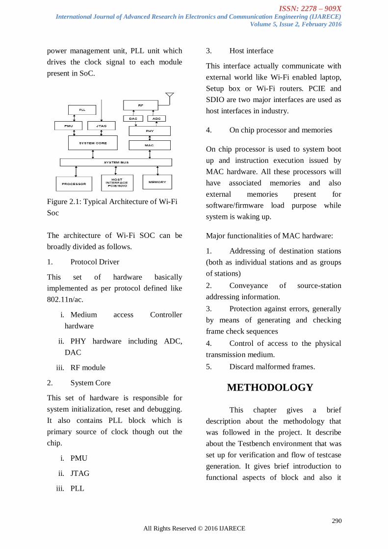
2.2 TYPICAL ARCHITECTURE
OF WLAN SoC
The typical architecture of wireless
local area network (WLAN) SoC with all
integrated modules is shown in Figure 2.2.
It includes protocol driver system which is
having MAC, PHY and RF modules, host
interface modules like PCIE or SDIO,
802.11
protocal
year Frequen
cy(GHz)
Bandwidt
h(MHZ)
Max. Data
Rate(Mbit/s)
MIMO Indoor
Range
(m)
Outdoor
Range(
m)
802.11 1997 2.4 22 2 No 20 100
A 1999 5/3.7 20 54 No 35 120
B 1999 2.4 22 11 No 35 140
G 2003 2.4 20 54 No 38 140
N 2009 2.4/5 20,40 65,135 4 70 250
Ac 2013 5 20,40,80,
160
86,180,390,7
80
8 35 250
ISSN: 2278 – 909X International Journal of Advanced Research in Electronics and Communication Engineering (IJARECE)
Volume 5, Issue 2, February 2016
290
All Rights Reserved © 2016 IJARECE
power management unit, PLL unit which
drives the clock signal to each module
present in SoC.
Figure 2.1: Typical Architecture of Wi-Fi
Soc
The architecture of Wi-Fi SOC can be
broadly divided as follows.
1. Protocol Driver
This set of hardware basically
implemented as per protocol defined like
802.11n/ac.
i. Medium access Controller
hardware
ii. PHY hardware including ADC,
DAC
iii. RF module
2. System Core
This set of hardware is responsible for
system initialization, reset and debugging.
It also contains PLL block which is
primary source of clock though out the
chip.
i. PMU
ii. JTAG
iii. PLL
3. Host interface
This interface actually communicate with
external world like Wi-Fi enabled laptop,
Setup box or Wi-Fi routers. PCIE and
SDIO are two major interfaces are used as
host interfaces in industry.
4. On chip processor and memories
On chip processor is used to system boot
up and instruction execution issued by
MAC hardware. All these processors will
have associated memories and also
external memories present for
software/firmware load purpose while
system is waking up.
Major functionalities of MAC hardware:
1. Addressing of destination stations
(both as individual stations and as groups
of stations)
2. Conveyance of source-station
addressing information.
3. Protection against errors, generally
by means of generating and checking
frame check sequences
4. Control of access to the physical
transmission medium.
5. Discard malformed frames.
METHODOLOGY
This chapter gives a brief
description about the methodology that
was followed in the project. It describe
about the Testbench environment that was
set up for verification and flow of testcase
generation. It gives brief introduction to
functional aspects of block and also it
ISSN: 2278 – 909X International Journal of Advanced Research in Electronics and Communication Engineering (IJARECE)
Volume 5, Issue 2, February 2016
291
All Rights Reserved © 2016 IJARECE
introduces the gate level simulation
methodology with SDF.
3.1 TEST BENCH SETUP
A test bench or testing workbench
is a virtual environment used to verify the
correctness or soundness of a design or
model. Test bench refers to an
environment in which the product under
development is tested with the aid of
software and hardware tools.
3.1.1 TEST BENCH ARCHITECTURE
The test bench architecture which
is used for current SoC is shown in Figure
3.1. It mainly contains input stimuli, test
bench and device under test (DUT). A
directed TCL script is the input stimuli for
test bench which have default settings and
set of scenarios to be verified. A typical
SoC have host interfaces PCIE, SDIO, etc.
and JTAG interface.
Figure 3.1: Test Bench Architecture
PCIE and SDIO can be access through the
PCIE interface and SDIO interface
respectively of DUT. JTAG can be access
through the GPIO (general purpose
input/output) pins. PCI master will drive
applied input stimulus to target module
like PCIE, SDIO or JTAG through PCI
BUS. We need to specify in our test case
on which interface test case needs to run.
All testcases can be run though any
interface by providing interface command
and the script will take care of handling of
choosing interfaces.
3.1.2 TEST CASE GENERATION AND
VERIFICATION
The flow of generating test case and its
verification is shown in Figure 3.2.
Figure 3.2: Test Case Generation and
Verification Flow
As shown in figure, the design modules
and respective test bench modules are
compiled and elaborated using simulation
tool. Using SoC specific scripting file
generate directed test case which contains
all the initial settings, interface (jtag, pcie,
sdio, etc) to run the test case and input file
having set of scenarios to be verified. Now
this directed test case run on simulation
tool. Check for any errors which might be
ISSN: 2278 – 909X International Journal of Advanced Research in Electronics and Communication Engineering (IJARECE)
Volume 5, Issue 2, February 2016
292
All Rights Reserved © 2016 IJARECE
due to input directed test files or debug
any design issues using debugging tools. If
test is failing due to scrip errors update
then and re run the test case and update. If
test case failing due to design issues report
bugs to respective designers and after
design fix compile and elaborate again and
run the test case. The above steps needs to
be follow till test case pass and then
update the status.
3.2 FUNCTIONAL DESCRIPTION OF
MODULES
3.2.1 Power Management Unit
In low power design a set of
methods are used to reduce power
consumption of SoC. Out of all methods
Power management unit especially plays
crucial role in low power consumption. So
in almost all the SoC, power management
is being integrated. Power management
Unit (PMU) is the most important core
which manages clock/reset and power
resources for the entire chip. The
functioning of PMU is given high priority
as many cores function on the clocks
driven by it from the Phase Locked Loop
(PLL).
PMU dynamically selects clocks to be
operated, based on request from one or
more cores and availability of resources.
The PMU manages the power and clock
resources for the entire chip, including
Clock/Reset Management, Dynamic Clock
control of Throughput clock, Low Power
Clock and Ideal Mode Clock for all the
modules of SoC. Driving clocks from PLL
and their management. Generation of
power island-specific resets, extended
Power On Reset (POR). Power
Management like Controlling LPO clock
frequency. Power Island on/off control that
makes some resources off depending on
the necessity .Strapping options to control
power-up mode
The Power Management Unit (PMU)
controls the oscillators and clocks with the
capability of enabling or disabling the
clock to the different peripherals
individually in addition to enabling or
disabling and configuring the available
oscillators. This allows for minimizing
energy consumption by disabling the clock
for unused peripherals or having them run
at lower frequencies.
Resource Management:
Resource management contains the
information about resource power
up/down sequence to be follow for all the
states. Each state has the dependency on
other states which must be powered
up/down before the present state powered
up/down. It also contains the power
up/down time for each resource in
sequence.
3.2.2 Clock Selection Module
PMU clock select module will
decides output clock to be selected, based
on clock request from one or more cores as
well as on resource availability status. Any
core request Throughput clock its checks
whether resource current state is
throughput avail, if state is throughput
avail then its selects throughput as system
ISSN: 2278 – 909X International Journal of Advanced Research in Electronics and Communication Engineering (IJARECE)
Volume 5, Issue 2, February 2016
293
All Rights Reserved © 2016 IJARECE
clock. If one core requests throughput
clock and another core request Low power
clock, then its gives the priority to
throughput clock if throughput clock is
available or it selects Low power clock as
system clock. Clock select block follows
the below priority in selecting output
clocks.
Throughput clock > Low power clock >
Ideal mode clock
Figure 3.3: Clock Select Module
.
3.2.3 Clock Generation Block and PLL
The clock generation block is
shown in Figure 3.4. Clock divider block
gives the wide range of frequency signals
which goes to different cores present on
SoC. In clock divider block VCO
frequency is divided by frequency dividers
for accomplishing all cores wide range of
clock frequency requirements. Finally
these frequencies are given to clock select
logic block and output clocks can be select
using clock_sel signal and request from
individual cores which is output from
PMU block.
Figure 3.4: Clock Generation Block
Phased- Locked Loop:
Phase Locked Loop (PLL) is a
fundamental part of radio, wireless and
telecommunication
Technology. The PLL circuit performs
frequency multiplication, via a negative
feedback mechanism, to generate the
output frequency Fvco, in terms of the
phase detector comparison frequency, Fr.
The phase-locked loop allows stable high
frequencies to be generated from a low-
frequency reference. Any system that
requires stable high frequency tuning can
benefit from the PLL technique.
Registers (PMU and PLL):
The default control values for PMU
core and PLL block present in these
registers. Resource management and clock
requests done through the PMU registers.
PLL registers have default divider integer
and fractional values. Clocks request from
MAC and PHY and clock gating can be
done through PLL registers.
ISSN: 2278 – 909X International Journal of Advanced Research in Electronics and Communication Engineering (IJARECE)
Volume 5, Issue 2, February 2016
294
All Rights Reserved © 2016 IJARECE
3.2.4 Clock Gating
Clock gating is a popular technique
used in many synchronous circuits for
reducing dynamic power dissipation.
Clock gating saves power by adding more
logic to a circuit to prune the clock tree.
Pruning the clock disables portions of the
circuitry so that the flip-flops in them do
not have to switch states. Switching states
consumes power. When not being
switched, the switching power
consumption goes to zero, and
only leakage currents are incurred.
Figure 3.5: Latch Based Clock Gating
Clock gating works by taking the enable
conditions attached to registers, and uses
them to gate the clocks. Therefore it is
imperative that a design must contain these
enable conditions in order to use and
benefit from clock gating. This clock
gating process can also save significant die
area as well as power, since it removes
large numbers of muxes and replaces them
with clock gating logic. This clock gating
logic is generally in the form of
"Integrated clock gating" (ICG) cells.
However, note that the clock gating logic
will change the clock tree structure, since
the clock gating logic will sit in the clock
tree.
Clock gating logic can be added into a
design in a variety of ways:
1. Coded into the RTL code as enable
conditions that can be
automatically translated into clock
gating logic by synthesis tools (fine
grain clock gating).
2. Inserted into the design manually
by the RTL designers (typically as
module level clock gating) by
instantiating library specific ICG
(Integrated Clock Gating) cells to
gate the clocks of specific modules
or registers.
3. Semi-automatically inserted into
the RTL by automated clock gating
tools. These tools either insert ICG
cells into the RTL, or add enable
conditions into the RTL code.
These typically also offer
sequential clock gating
optimizations.
Any RTL modifications to improve clock
gating will result in functional changes to
the design (since the registers will now
hold different values) which need to be
verified. Sequential clock gating is the
process of extracting/propagating the
enable conditions to the
upstream/downstream sequential elements,
so that additional registers can be clock
gated.
ISSN: 2278 – 909X International Journal of Advanced Research in Electronics and Communication Engineering (IJARECE)
Volume 5, Issue 2, February 2016
295
All Rights Reserved © 2016 IJARECE
3.3 METHODOLOGY OF GATE
LEVEL SIMULATIONS EXECUTION
3.3.1 Introduction to Timing Analysis
Timing and delay information and
analysis are very important and parallel
flow in the ASIC design process because it
brings higher level degree of realism to be
implemented into the circuit model.
Typically this timing information does not
include in Hardware description model and
the outputs of these modules are
instantaneously got resolved. This strips
the designer of important details such as
propagation delay, pulse width, setup and
hold times. The setup and hold violations
could very easily lead to incorrect state
transitions from the design which is not
intended as per the functional
requirements.
Timing characterization of entire design is
tedious and time consuming endeavor and
it is often ignored process in a design. So
this allows most designers to be primarily
concerned with the functional correctness
of a circuit. In the past, this approach may
have been adequate for lower speed
designs. However, as technology continues
to mature, meeting timing constraints for
designs becomes just as important as
functional correctness.
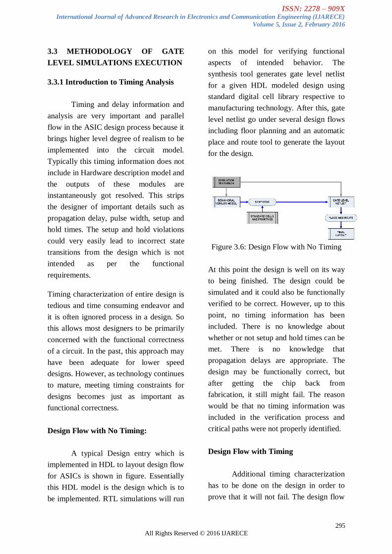
Design Flow with No Timing:
A typical Design entry which is
implemented in HDL to layout design flow
for ASICs is shown in figure. Essentially
this HDL model is the design which is to
be implemented. RTL simulations will run
on this model for verifying functional
aspects of intended behavior. The
synthesis tool generates gate level netlist
for a given HDL modeled design using
standard digital cell library respective to
manufacturing technology. After this, gate
level netlist go under several design flows
including floor planning and an automatic
place and route tool to generate the layout
for the design.
Figure 3.6: Design Flow with No Timing
At this point the design is well on its way
to being finished. The design could be
simulated and it could also be functionally
verified to be correct. However, up to this
point, no timing information has been
included. There is no knowledge about
whether or not setup and hold times can be
met. There is no knowledge that
propagation delays are appropriate. The
design may be functionally correct, but
after getting the chip back from
fabrication, it still might fail. The reason
would be that no timing information was
included in the verification process and
critical paths were not properly identified.
Design Flow with Timing
Additional timing characterization
has to be done on the design in order to
prove that it will not fail. The design flow
ISSN: 2278 – 909X International Journal of Advanced Research in Electronics and Communication Engineering (IJARECE)
Volume 5, Issue 2, February 2016
296
All Rights Reserved © 2016 IJARECE
should be changed to include delay
extraction and back annotation.
Figure 3.7: Design Flow with Timing
using Back Annotation
Delay extraction will allow us to get
delays from the placed and routed design.
Back annotation will then take this delay
information and place it back into the gate
level Verilog model. Gate level
simulations will carry out on this netlist for
verifying design after place and route to
ensure indeed functionality. At this point,
the design can be simulated with timing
information to ensure both functional and
timing correctness.
3.3.2 Motivation for running gate level
simulations
RTL simulation is the basic
requirement to signoff design cycle, but as
operating frequencies of SOC
tremendously increased whole design need
to properly verify functionally as well as
for timing requirements. This is
accomplishing by carry out static timing
analysis and Dynamic timing analysis.
Static timing analysis does not depend on
any data or logic inputs, applied at the
input pins. The input to an STA tool is the
routed netlist, clock definitions (or clock
frequency) and external environment
definitions. The STA will validate whether
the design could operate at the rated clock
frequency, without any timing violations.
Limitations of STA lead to increasing
trend in the industry to run gate level
simulations (GLS) before going into the
last stage of chip manufacturing.
Improvements in static verification tools
like Static timing analysis (STA) and
Equivalence Checking (EC) have
leveraged GLS to some extent but so far
none of the tools have been able to
completely remove it. GLS still remains a
significant step of the verification cycle
footprint.
The main reasons for running GLS are
as follows:
1. To verify the power up and reset
operation of the design and also to
check that the design does not have
any unintentional dependencies on
initial conditions.
2. To give confidence in verification of
low power structures, absent in RTL
and added during synthesis.
3. It is a probable method to catch multi
cycle paths if tests exercising them
are available.
4. Power estimation is done on netlist
for the power numbers.
5. To verify DFT structures absent in
RTL and added during or after
synthesis. Scan chains are generally
inserted after the gate level netlist has
been created. Hence, gate level
ISSN: 2278 – 909X International Journal of Advanced Research in Electronics and Communication Engineering (IJARECE)
Volume 5, Issue 2, February 2016
297
All Rights Reserved © 2016 IJARECE
simulations are often used to
determine whether scan chains are
correct. GLS is also required to
simulate ATPG patterns.
6. Tester patterns (patterns to screen
parts for functional or structural
defects on tester) simulations are done
on gate level netlist.
7. To help reveal glitches on edge
sensitive signals due to combination
logic. Using both worst and best-case
timing may be necessary.
8. It is a probable method to check the
critical timing paths of asynchronous
designs that are skipped by STA.
9. To avoid simulation artifacts that can
mask bugs at RTL level (because of
no delays at RTL level).
10. Could give insight to constructs that
can cause simulation-synthesis
mismatch and can cause issues at the
netlist level.
11. To check special logic circuits and
design topology that may include
feedback and/or initial state
considerations, or circuit tricks. If a
designer is concerned about some
logic then this is good candidate for
gate simulation. Typically, it is a good
idea to check reset circuits in gate
simulation. Also, to check if we have
any uninitialized logic in the design
which is not intended and can cause
issues on silicon.
12. To check if design works at the
desired frequency with actual delays
in place.
13. It is a probable method to find out the
need for synchronizers if absent in
design. It will cause “x” propagation
on timing violation on that flop.
Figure 3.8: GLS Execution flow
Execution Strategy for GLS
1. Planning the test-suite wisely to be
run in GLS
In highly integrated products it is not
possible to run gate simulation for all the
SoC tests due to the simulation and debug
time required .Therefore, the list of vectors
which are to be run in GLS has be selected
judiciously. The possible candidates for
this list are
i. Testcases involving
initialization, boot up.
ii. All the blocks of the design
must have atleast one testcase for
GLS.
iii. Testcases checking clock
source switching.
ISSN: 2278 – 909X International Journal of Advanced Research in Electronics and Communication Engineering (IJARECE)
Volume 5, Issue 2, February 2016
298
All Rights Reserved © 2016 IJARECE
iv. Cases checking clock
frequency scaling.
v. Asynchronous paths in the
design.
vi. Testcases which check
entry/exit from different modes
of the design.
vii. Dedicated tests for timing
exceptions in the STA.
viii. Patterns covering multi
clock domain paths in the design
ix. Multi reset patterns are a
good candidate for GLS
It must also be made sure that the test
cases selected to be run in GLS are
targeting the maximum desired operating
frequency of the design. Should there be
no time constraints, all tests run in RTL
simulations can be rerun in GLS. Also, if
there are no tests fulfilling the criteria
mentioned above, then they should be
coded.
2. Test bench updates for GLS
A list of all the synchronizer flops is
generated using CDC tools. Also, other
known asynchronous paths where timing
checks needs to be turned off are analyzed
and complete list of such flops is prepared
which also includes reset synchronizers.
The timing checks are turned off on all
such flops to avoid any redundant
debugging, otherwise they will cause “x”
corruption in GLS. This work should be
ideally done before the SDF arrives .It
may happen that the name of the
synchronizers in RTL and the netlist are
different. All such flops should be updated
as per netlist .Also, the correct standard
cell libraries, correct models of analog
blocks, etc. need to be picked for GLS.
3. Initialization of non-resettable
flops in the design
One of the main challenges in GLS is the
“x” propagation debug. X corruption may
be caused by a number of reasons such as
timing violations, uninitialized memory
and non resettable flipflops. There are
uninitialized flops in design which by
architecture are guaranteed to not cause
any problems (if they settle to any value at
start). Thus, there is a need to find out all
such flops in the design (which are
reviewed with designers) and initialize
them to some random value (either 0 or 1)
so as to mimic silicon.
4. Unit delay GLS for Testbench
cleanup
This step is not compulsory but is
generally very fruitful if employed in the
GLS execution. The setup is done for unit
delay GLS (no SDF) and the testcases that
are planned to be run on gate level are run
with this setup to clean the testbench. This
is done because the unit delay simulations
are relatively faster (than those with SDF)
and all the testbench/testcase related issues
can be resolved here (for example -
change probed logic hierarchy from rtl to
gate, wrong flow of testcase, use of
uninitialized variables in the test cases that
can cause corruption when read via core,
etc). Running the unit delay GLS is
recommended because one can catch most
ISSN: 2278 – 909X International Journal of Advanced Research in Electronics and Communication Engineering (IJARECE)
Volume 5, Issue 2, February 2016
299
All Rights Reserved © 2016 IJARECE
of the testbench/testcase issues before the
arrival of SDF. After the SDF arrives,
focus should be more on finding the real
design/timing issues, so we need to make
sure that the time does not get wasted in
debugging the testcase related issues at
that time.
5.Annotation warnings cleanup on SDF
When the SDF is delivered to verification
team, then the simulations are run with the
SDF/netlist. Specific tool switches need to
be passed which picks us the SDF and tries
to annotate the delays mentioned in the
SDF to the corresponding instances/arcs in
the netlist. This is known as back-
annotation.
During this process, many annotation
warnings are encountered which need to
be analyzed and either sorted out or
waived off by the design team. Most
important warnings which need to be
looked into are the ones which are due to
non-existent paths i.e. the SDF has an arc
but netlist does not have it. Also, there can
be mismatch between the simulation
model “specify” block and .lib of the IP.
5. Running GLS with SDF:
Early SDF (for initial debug) this step
involves use of a SDF in which timing is
met at a lower frequency than target and
GLS can be run at that frequency. This
helps in cleaning up the flow and finding
certain issues before the final SDF arrives.
This step starts with the SDF in which
timing is met at target frequency. The
entire setup is done and the planned
pattern-suite is run on this setup and
failures needs to be debugged according to
a priority list which should be made before
hand. All the high priority patterns need to
be debugged first.
Challenges faced during GLS setup
GLS with SDF delays annotated is
usually very slow and time consuming. A
lot of planning is needed to wisely select
the patterns that need to be simulated on
netlist. Run-time for these tests and
memory requirements for dump and logs
must also be considered. Identifying the
optimal list of tests to efficiently utilize
GLS in discovering functional or timing
bugs is tough. These are to be decided with
discussions with timing team and design
team on which paths are timing
critical/asynchronous and needs to be
checked.
GLS is much more difficult than RTL
simulations as delays of gates,
interconnects comes into picture and RTL
assumptions for arrival of data/clock may
mismatch causing failures. During the
initial stages of GLS, identifying the list of
flops/latches that needs to be initialized
(forced reset) is a big hurdle. The
pessimism in simulations would cause “x”
on the output of all such components
without proper reset, bringing GLS to a
standstill. If approved by design and
architecture team, these initializations
should be done to move forward.
ISSN: 2278 – 909X International Journal of Advanced Research in Electronics and Communication Engineering (IJARECE)
Volume 5, Issue 2, February 2016
300
All Rights Reserved © 2016 IJARECE
During synthesis, the port/nets may get
optimized or re-named to meet the timing
on these paths. Monitors/Assertions
hooked in Testbench during RTL
simulations need to be revised for GLS to
make sure the intended net is getting
probed. Also, in netlist there can be
inverters that can be inserted on that signal
driver due to boundary optimization and
can cause false failures (not having any
design issues). This is really tough to
figure out and debug.
If the gate level simulation with SDF is
done without a complete synchronizer list,
then failure debug to find such cases on
gate level is quite cumbersome. Multiple
debug iterations may happen in GLS to
find out many such flops.
Debugging the netlist simulations is a big
challenge. In GLS, models of the cells
make the output “x” if there is a timing
violation on that cell. Identifying the right
source of the problem requires probing the
waveforms at length which means huge
dump files or rerunning simulations
multiple times to get the right timing
window for violations. The latest tools are
offering “x” tracing techniques for quickly
tracing the source of “x” propagation.
Such tool features need to be explored. All
said and done, it can be concluded that one
requires a lot of patience while debugging
the GLS waveforms.
In short, despite being a time consuming
activity and having many challenges in
setup and debug, GLS is a great
confidence booster in the quality of the
design. It can uncover certain hidden
issues which get missed out or difficult to
find by RTL simulations. This is the
reason many organizations prefer this
activity before tape-out because it is more
close to the actual silicon and gives a fairly
good idea about how the design will
behave in real. The probability of having
sound sleep after tape out improves with
GLS.
3.3.3 Standard Delay Format and
Generation of SDF Files
This section is an overview of the
Standard Delay Format (SDF). The best
description of what the SDF is can be
found in the opening paragraph of the
IEEE Draft Standard.
“The Standard Delay Format (SDF) was
designed to serve as a simple textual
medium for communicating timing
information and constraints between
electronic design automation tools. The
original version was designed by Rajit C.
Chandra in 1990 while at Cadence Design
Systems, and was intended as a means of
communicating macrocell and
interconnects delays from Gate Ensemble
to Verilog-XL, Veritime and other stand-
alone tools requiring timing data“
The SDF was designed from the ground up
to be an easy way to convey timing
information to a simulator. The SDF file
can furthermore be utilized by other design
tools. It can be leveraged to convey design
constraints identified during timing
analysis to layout tools (forward
annotation) and it can also be used for post
ISSN: 2278 – 909X International Journal of Advanced Research in Electronics and Communication Engineering (IJARECE)
Volume 5, Issue 2, February 2016
301
All Rights Reserved © 2016 IJARECE
layout timing analysis and simulation
(back annotation).
The figure on the following page depicts
the general flow of how to use SDF files in
an ASIC design. The SDF files are most
often generated by a delay calculator. This
delay calculator uses information from a
placed and routed design. After the SDF
file is generated by the timing calculator,
simulator will be used to back annotate
this delay information into the design
description. Timing characteristics of
ASICS are strongly influenced by
interconnect affects. This is why back
annotation is most often done post layout.
The SDF imposes no restrictions on the
precision of the timing data being
represented. This implies that the accuracy
of the timing data is dependent on the
accuracy of the timing calculator.
Figure 3.9: SDF Generation and Back
Annotation
Timing Checks
The SDF has many different timing
checks available. The important ones are
the setup, hold, recovery and width timing
checks. They will be discussed below. The
format for the timing checks is a timing
check definition followed by the
appropriate delay information. This delay
information varies for each timing check.
Setup Time: This is the setup timing
check. It is defined as the time before a
clock that the signal must remain stable in
order for that signal to successfully be
stored into the device. The format is the
keyword SETUP followed by an input port
specification followed by an output port
specification followed by the delay values.
Figure 3.10: Setup Time
Example: (INSTANCE x.a)
(TIMINGCHECK
(SETUP din (posedge clk)
(12))
- - - -
- - - -
)
Hold Time: This is the hold timing check.
It is defined as the time after a clock edge
in which a signal must remain stable. The
format is the keyword HOL followed by
an input port specification followed by an
output port specification followed by the
delay values.
ISSN: 2278 – 909X International Journal of Advanced Research in Electronics and Communication Engineering (IJARECE)
Volume 5, Issue 2, February 2016
302
All Rights Reserved © 2016 IJARECE
Figure 3.11: Hold Time
Example: (INSTANCE x.a)
(TIMINGCHECK
( HOLD din (posedge clk)
(10))
- - - -
- - - -
)
Setup and Hold Combined: This is a
combination of setup and hold. Its format
is the keyword SETUPHOLD followed by
input port followed by output port
followed by setup delay values followed
by hold delay values.
Figure 3.12: Setup and Hold Time
Example: (INSTANCE x.a)
(TIMINGCHECK
(SETUPHOLD din
(posedge clk) (12) (9.5) (CCOND ~reset))
- - - -
- - - -
)
Recovery Time: The recovery time is
defined as the limit of the time between
the release of an asynchronous control
signal from the active state and the next
active clock edge. The format is the
keyword RECOVERY followed by an
input port followed by an output port
followed by the delay values.
Figure 3.13: Recovery Time
Example: (INSTANCE x.b)
(TIMINGCHECK
( RECOVERY (posedge
clearbar) (posedge clk) (10.5))
- - - -
- - - -
)
Removal Time: The removal shall specify
limit values for removal timing checks. A
removal timing check is a limit of the time
between an active clock edge and the
release of an asynchronous control signal
from the active state, for example between
the clock and the clearbar for a flip-flop. If
the release of the clearbar occurs too soon
after the active edge of the clock, the state
of the flip-flop shall become uncertain it
could be the value set by the clearbar, or it
could be the value clocked into the flip-
flop from the data input. In other respects,
a removal check is similar to a hold check.
The syntax for removal timing check is
described in Syntax
ISSN: 2278 – 909X International Journal of Advanced Research in Electronics and Communication Engineering (IJARECE)
Volume 5, Issue 2, February 2016
303
All Rights Reserved © 2016 IJARECE
Figure 3.14: Removal Time
Example: (INSTANCE x.b)
(TIMINGCHECK
( REMOVAL (posedge
clearbar) (posedge clk) (10.5))
- - - -
- - - -
)
Width: The width timing check specifies a
limit for a minimum pulse width. If the
signal has unequal phases, two pulse
widths can be specified.
Figure 3.15: Width Timing Check
Example: (INSTANCE x.b)
(TIMINGCHECK
(WIDTH (posedge clk)
(30))
(WIDTH (negedge clk)
(16.5))
- - - -
- - - -
)
Verilog Back Annotation:
Back annotation is the process by which
timing information is added into a design
so that the design can be simulated with
realistic delays. For this section back
annotation requires that a SDF file has
been generated for a design and that
specify blocks with path delays have been
defined for cells.
3.3.4 Importance of Corner case
Simulations
The propagation delay varies
significantly due to variations in transistor
operating parameters over the
environmental changes which include
operating supply voltages and temperature
variations and process changes. Process
variations are due to variations in the
manufacture conditions such as
temperature, pressure and dopant
concentrations.
A higher voltage makes a cell
faster and hence the propagation delay is
reduced
A higher temperature will decrease
the threshold voltage
Variations in the process parameter
leads to transistors have different transistor
lengths throughout the chip. This makes
the propagation delay to be different.
These variations can be modelled under
different corner case like fast (minimum
delay) and slow (maximum delay) and
these are shown in Table.
ISSN: 2278 – 909X International Journal of Advanced Research in Electronics and Communication Engineering (IJARECE)
Volume 5, Issue 2, February 2016
304
All Rights Reserved © 2016 IJARECE
Table 3.1: Corner cases
So apart from typical SDF generation we
need generate SDF for maximum and
minimum corners too using worst case
conditions and finally using these SDF,
carry out gate level simulations for
verifying the design under corner
conditions this eventually boost the
confident on designed modules. Run slow
corner simulations for delay analysis and
fast corner simulations for power and race
conditions like hold time analysis.
3.4 TOOLS USED IN PROJECT
3.4.1 Cadence Ncsim Simulator
Ncsim from Cadence is used as a
solution for all simulation and verification
environments. It provides engines for
Coverage, constraint solver, Assertions to
name a few. Ncsim provides many options
to collect and analyze the simulation data
effectively and debug them using
waveform dumping. This tool is used for
compilation and elaboration of both
Verilog and VHDL model and commands
can be given from console or GUI
provided by vendor.
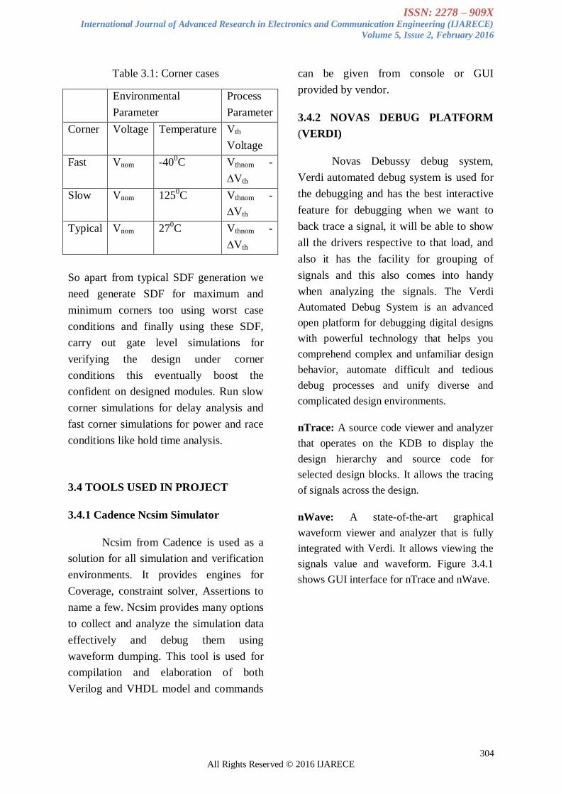
3.4.2 NOVAS DEBUG PLATFORM
(VERDI)
Novas Debussy debug system,
Verdi automated debug system is used for
the debugging and has the best interactive
feature for debugging when we want to
back trace a signal, it will be able to show
all the drivers respective to that load, and
also it has the facility for grouping of
signals and this also comes into handy
when analyzing the signals. The Verdi
Automated Debug System is an advanced
open platform for debugging digital designs
with powerful technology that helps you
comprehend complex and unfamiliar design
behavior, automate difficult and tedious
debug processes and unify diverse and
complicated design environments.
nTrace: A source code viewer and analyzer
that operates on the KDB to display the
design hierarchy and source code for
selected design blocks. It allows the tracing
of signals across the design.
nWave: A state-of-the-art graphical
waveform viewer and analyzer that is fully
integrated with Verdi. It allows viewing the
signals value and waveform. Figure 3.4.1
shows GUI interface for nTrace and nWave.
Environmental
Parameter
Process
Parameter
Corner Voltage Temperature Vth
Voltage
Fast Vnom -400C Vthnom -
∆Vth
Slow Vnom 1250C Vthnom -
∆Vth
Typical Vnom 270C Vthnom -
∆Vth
ISSN: 2278 – 909X International Journal of Advanced Research in Electronics and Communication Engineering (IJARECE)
Volume 5, Issue 2, February 2016
305
All Rights Reserved © 2016 IJARECE
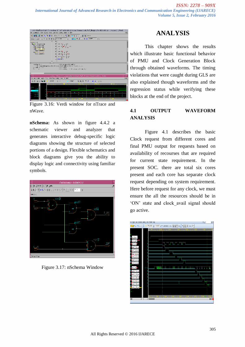
Figure 3.16: Verdi window for nTrace and
nWave.
nSchema: As shown in figure 4.4.2 a
schematic viewer and analyzer that
generates interactive debug-specific logic
diagrams showing the structure of selected
portions of a design. Flexible schematics and
block diagrams give you the ability to
display logic and connectivity using familiar
symbols.
Figure 3.17: nSchema Window
ANALYSIS
This chapter shows the results
which illustrate basic functional behavior
of PMU and Clock Generation Block
through obtained waveforms. The timing
violations that were caught during GLS are
also explained though waveforms and the
regression status while verifying these
blocks at the end of the project.
4.1 OUTPUT WAVEFORM
ANALYSIS
Figure 4.1 describes the basic
Clock request from different cores and
final PMU output for requests based on
availability of recourses that are required
for current state requirement. In the
present SOC. there are total six cores
present and each core has separate clock
request depending on system requirement.
Here before request for any clock, we must
ensure the all the resources should be in
„ON‟ state and clock_avail signal should
go active.
ISSN: 2278 – 909X International Journal of Advanced Research in Electronics and Communication Engineering (IJARECE)
Volume 5, Issue 2, February 2016
306
All Rights Reserved © 2016 IJARECE
Figure 4.1: Output waveform shows
Clock request from different cores and
PMU output for requests.
Figure 4.2 describes how exactly PMU
determines the priority over the request
and availability of resources. Here it
explains PMU final clock select for a
single core with multiple clock requests.
Initially all clocks (H_clk, LP_clk and
IM_clk) are available and there is request
for H_clk so T_clk is selected as final
clock to be run. After some time T_clk
turned off, now PMU look for next
available clock and LP_clk is available so
PMU select LP_clk as final clock even
though there is a request for T_clk.
Similarly same priority is followed for
LP_clk over IM_clk.
Figure 4.2: Output waveform shows PMU
priority over request and availability of
resource
Figure 4.3 explains programming of PLL
dividers and respective output frequency
on PLL VCO output. Here PLL is
provided with set registers which can be
program as per require of
Figure 4.3: Output waveform shows
programming of PLL dividers and
respective frequency
clock frequency. There are two parts in
divider registers first part is integer divider
and fractional part for fine tune of signal
frequency. In this the reset sequence of
PLL has been shown and PLL is in close
loop and it must not lost its lock during
small step change of frequencies which
can be observed in this waveform.
Figure 4.4 describes clock gating
implematation which is a low power
technique.Here clock gating block
generates output signal based on clock
enable during which gives output as input
and rest of the skips the pulses. The
number of pulses need to be skip and
number of pulses need to pass can be
program through registers and using these
values internal timers will toggle clock
enable signal. In following example total
seven pulses have been skipped and only
three pulses are present on output signal
and this repeats for every ten pulses.
ISSN: 2278 – 909X International Journal of Advanced Research in Electronics and Communication Engineering (IJARECE)
Volume 5, Issue 2, February 2016
307
All Rights Reserved © 2016 IJARECE
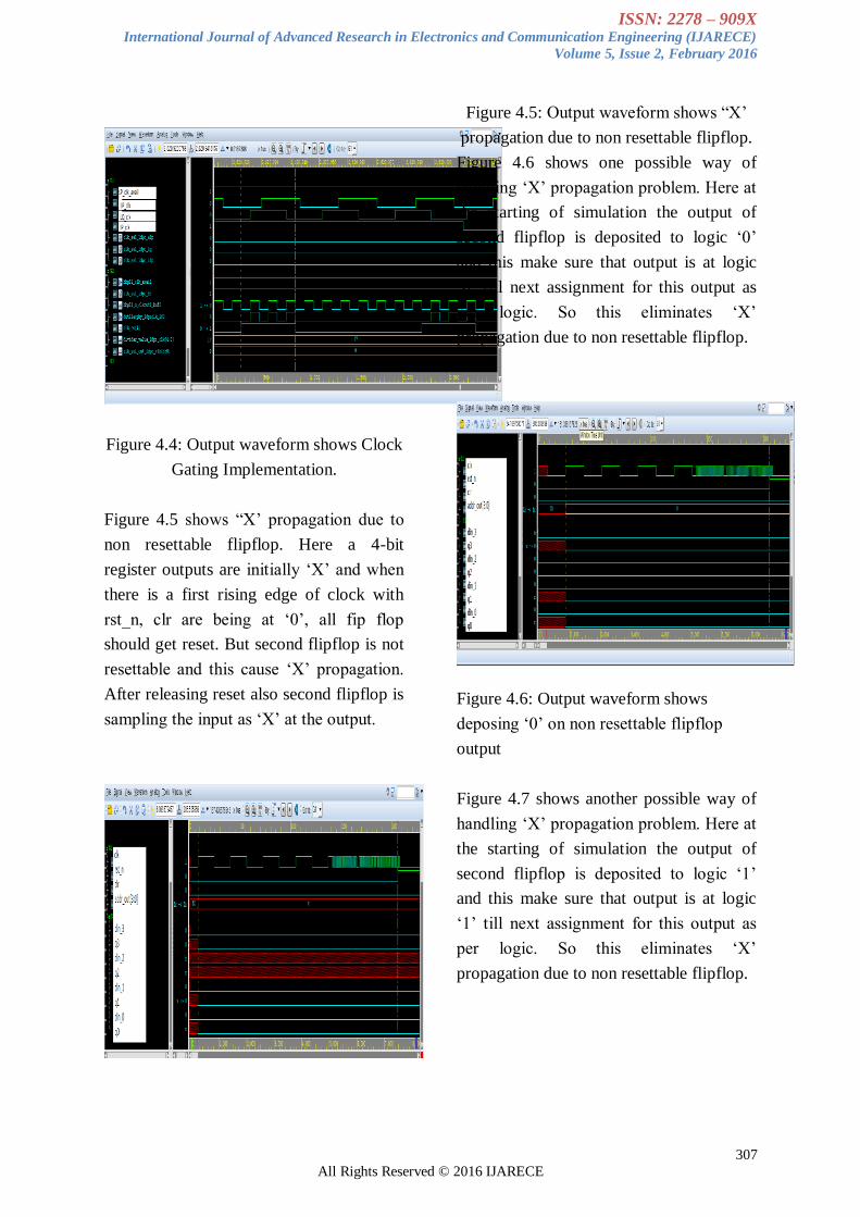
Figure 4.4: Output waveform shows Clock
Gating Implementation.
Figure 4.5 shows “X‟ propagation due to
non resettable flipflop. Here a 4-bit
register outputs are initially „X‟ and when
there is a first rising edge of clock with
rst_n, clr are being at „0‟, all fip flop
should get reset. But second flipflop is not
resettable and this cause „X‟ propagation.
After releasing reset also second flipflop is
sampling the input as „X‟ at the output.
Figure 4.5: Output waveform shows “X‟
propagation due to non resettable flipflop.
Figure 4.6 shows one possible way of
handling „X‟ propagation problem. Here at
the starting of simulation the output of
second flipflop is deposited to logic „0‟
and this make sure that output is at logic
„0‟ till next assignment for this output as
per logic. So this eliminates „X‟
propagation due to non resettable flipflop.
Figure 4.6: Output waveform shows
deposing „0‟ on non resettable flipflop
output
Figure 4.7 shows another possible way of
handling „X‟ propagation problem. Here at
the starting of simulation the output of
second flipflop is deposited to logic „1‟
and this make sure that output is at logic
„1‟ till next assignment for this output as
per logic. So this eliminates „X‟
propagation due to non resettable flipflop.
ISSN: 2278 – 909X International Journal of Advanced Research in Electronics and Communication Engineering (IJARECE)
Volume 5, Issue 2, February 2016
308
All Rights Reserved © 2016 IJARECE
Figure 4.7: Output waveform shows
deposing „1‟ on non resettable flipflop
output.
Figure 4.8 shows setup time violation.
Here enabled signal and resetb of flipflop
are at logic „1‟ so input value is sampled at
output at rising edge of clock. But as
shown in figure the minimum amout of
time during which data at input is not
stable before clock edge which leads to
metastebility state of flipflop and this
makes flipflop output as „X‟
Figure 4.8: Output waveform shows setup
time violation
4.2 REGRESSION STATUS RESULTS
To know the amout verification
completed we run the regressions
periodocally or/and after any design
changes in RTL. Here these regressions
have been run for both RTL simulations
and gate level simulations though out the
projects. The following tables give
regression status for RTL and GLS
simulations of Chip1 and Chip2.
Table 4.1: Regression status for RTL
simulations of Chip1
Modul
e
Total no
of
Testcase
s
No. of
testcase
s
passed
at
starting
of
project
No. of
testcase
s
passed
at end
of
project
PMU 36 9 36
CGB 29 12 29
Table 4.2: Regression status for Gate
Level Simulations of Chip1
Modul
e
Total no
of
Testcase
s
No. of
testcase
s
passed
at
starting
of
project
No. of
testcase
s
passed
at end
of
project
PMU 13 5 13
CGB 15 4 15
ISSN: 2278 – 909X International Journal of Advanced Research in Electronics and Communication Engineering (IJARECE)
Volume 5, Issue 2, February 2016
309
All Rights Reserved © 2016 IJARECE
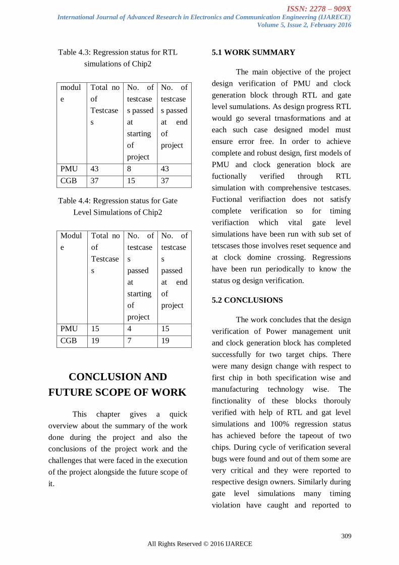
Table 4.3: Regression status for RTL
simulations of Chip2
modul
e
Total no
of
Testcase
s
No. of
testcase
s passed
at
starting
of
project
No. of
testcase
s passed
at end
of
project
PMU 43 8 43
CGB 37 15 37
Table 4.4: Regression status for Gate
Level Simulations of Chip2
Modul
e
Total no
of
Testcase
s
No. of
testcase
s
passed
at
starting
of
project
No. of
testcase
s
passed
at end
of
project
PMU 15 4 15
CGB 19 7 19
CONCLUSION AND
FUTURE SCOPE OF WORK
This chapter gives a quick
overview about the summary of the work
done during the project and also the
conclusions of the project work and the
challenges that were faced in the execution
of the project alongside the future scope of
it.
5.1 WORK SUMMARY
The main objective of the project
design verification of PMU and clock
generation block through RTL and gate
level sumulations. As design progress RTL
would go several trnasformations and at
each such case designed model must
ensure error free. In order to achieve
complete and robust design, first models of
PMU and clock generation block are
fuctionally verified through RTL
simulation with comprehensive testcases.
Fuctional verifiaction does not satisfy
complete verification so for timing
verifiaction which vital gate level
simulations have been run with sub set of
tetscases those involves reset sequence and
at clock domine crossing. Regressions
have been run periodically to know the
status og design verification.
5.2 CONCLUSIONS
The work concludes that the design
verification of Power management unit
and clock generation block has completed
successfully for two target chips. There
were many design change with respect to
first chip in both specification wise and
manufacturing technology wise. The
finctionality of these blocks thorouly
verified with help of RTL and gat level
simulations and 100% regression status
has achieved before the tapeout of two
chips. During cycle of verification several
bugs were found and out of them some are
very critical and they were reported to
respective design owners. Similarly during
gate level simulations many timing
violation have caught and reported to
ISSN: 2278 – 909X International Journal of Advanced Research in Electronics and Communication Engineering (IJARECE)
Volume 5, Issue 2, February 2016
310
All Rights Reserved © 2016 IJARECE
backend team and this cycle repeated till
end of project.
5.3 FUTURE SCOPE OF WORK
The developed scripts for verifying
scenorios were made as generic which
permits future chips can adopt these
testcases with less efforts which intern
reduce design cycle. All register read or
writes have made generic to all other chips
which are design phase or architecture
phase in which by giving base address
only we run all testcases as register set
index is fixed for all core registers and this
can be easily undertand by designers and
help them to reduce dubugging efforts.
The developed test bench setup and
set comprehensive testcases can easily
migrate to system verilog platform which
is popular language for verification in
industry which provides more feasible
constructs. The existing sequences in TCL
language can directy port to System
verilog platform and there is a scope of
increase in automation in new platform.
The next step after the verification
is followed by the backend flow, and any
issues that they come across during this
process will be brought to the notice of
front end designers if they are related to
functional issues and once they are fixed
the models are delivered to the SOC team
and it goes through one more verification
flow and after successful fabrication
comes as an product in next generation
Wi-Fi SOC.
REFERENCES
[1] Lulu Feng, “Design and application of
reusable SoC verification platform”, ASIC
(ASICON), 2011 IEEE 9th International
Conference on, pp 957-960, 2011
[2] Pankaj Chauhan, et al Verifying IP–
Core based System–On–Chip Designs,
IEEE International ASIC/SOC
Conference, September 1999.
[3] SoC Verification Business Unit Mentor
Graphics, Design Challenges Thrust on
SoC Process 2004
[4] Kong Weio Susanto “A verification
Platform for a System on Chip” University
of Glasgow UK - 2003.
[5] Petlin, O. Methodology and code
reuse in the verification of
telecommunication SOCs, ASIC/SOC
Conference, 2000. Proceedings, 13th
Annual IEEE International, pp 187-191,
2000
[6]
http://www.analog.com/library/analogDial
ogue/archives/33-03/phase/index.html
[7]
http://www.tcl.tk/man/tcl8.5/tutorial/tcltut
orial.html
[8]
http://www.standards.ieee.org/news/2014/i
eee_802_11ac_ballot.html


![ISSN: 2278 909X International Journal of Advanced Research in …ijarece.org/wp-content/uploads/2017/05/IJARECE-VOL-6... · 2017-05-14 · McLean [3] derived relations for the minimum](https://static.documents.pub/doc/80x56/5ea04bb213d2e0694433d80b/issn-2278-909x-international-journal-of-advanced-research-in-2017-05-14-mclean.jpg)


