15
June 10, 2002 11:03 vra23151_ch01 Sheet number 1 Page number 1 black 1 chapter 1 Design Concepts 1. e2–e4, c7–c6
June 10, 2002 11:03 vra23151_ch01 Sheet number 1 Page number 1 black
1
c h a p t e r
1Design Concepts
1. e2–e4, c7–c6

June 10, 2002 11:03 vra23151_ch01 Sheet number 2 Page number 2 black
2 C H A P T E R 1 • Design Concepts
This book is about logic circuits—the circuits from which computers are built. Proper understanding oflogic circuits is vital for today’s electrical and computer engineers. These circuits are the key ingredient ofcomputers and are also used in many other applications. They are found in commonly used products, such asdigital watches, various household appliances, CD players, and electronic games, as well as in large systems,such as the equipment for telephone and television networks.
The material in this book will introduce the reader to the many issues involved in the design of logiccircuits. It explains the key ideas with simple examples and shows how complex circuits can be derived fromelementary ones. We cover the classical theory used in the design of logic circuits in great depth because itprovides the reader with an intuitive understanding of the nature of such circuits. But throughout the book wealso illustrate the modern way of designing logic circuits, using sophisticated computer aided design (CAD)software tools. The CAD methodology adopted in the book is based on the industry-standard design languagecalled Verilog. Design with Verilog is first introduced in Chapter 2, and usage of Verilog and CAD tools isan integral part of each chapter in the book.
Logic circuits are implemented electronically, using transistors on an integrated circuit chip. With moderntechnology it is possible to fabricate chips that contain tens of millions of transistors, as in the case of computerprocessors. The basic building blocks for such circuits are easy to understand, but there is nothing simpleabout a circuit that contains tens of millions of transistors. The complexity that comes with the large size oflogic circuits can be handled successfully only by using highly organized design techniques. We introducethese techniques in this chapter, but first we briefly describe the hardware technology used to build logiccircuits.
1.1 Digital Hardware
Logic circuits are used to build computer hardware, as well as many other types of products.All such products are broadly classified as digital hardware. The reason that the name digitalis used will become clear later in the book—it derives from the way in which informationis represented in computers, as electronic signals that correspond to digits of information.
The technology used to build digital hardware has evolved dramatically over the pastfour decades. Until the 1960s logic circuits were constructed with bulky components, suchas transistors and resistors that came as individual parts. The advent of integrated circuitsmade it possible to place a number of transistors, and thus an entire circuit, on a singlechip. In the beginning these circuits had only a few transistors, but as the technologyimproved they became larger. Integrated circuit chips are manufactured on a silicon wafer,such as the one shown in Figure 1.1. The wafer is cut to produce the individual chips,which are then placed inside a special type of chip package. By 1970 it was possible toimplement all circuitry needed to realize a microprocessor on a single chip. Although earlymicroprocessors had modest computing capability by today’s standards, they opened thedoor for the information processing revolution by providing the means for implementationof affordable personal computers. About 30 years ago Gordon Moore, chairman of IntelCorporation, observed that integrated circuit technology was progressing at an astoundingrate, doubling the number of transistors that could be placed on a chip every 1.5 to 2 years.

June 10, 2002 11:03 vra23151_ch01 Sheet number 3 Page number 3 black
1.1 Digital Hardware 3
Figure 1.1 A silicon wafer (courtesy of Altera Corp.).
This phenomenon, informally known as Moore’s law, continues to the present day. Thus inthe early 1990s microprocessors could be manufactured with a few million transistors, andby the late 1990s it became possible to fabricate chips that contain more than 10 milliontransistors. Presently chips can have a few hundreds of millions of transistors.
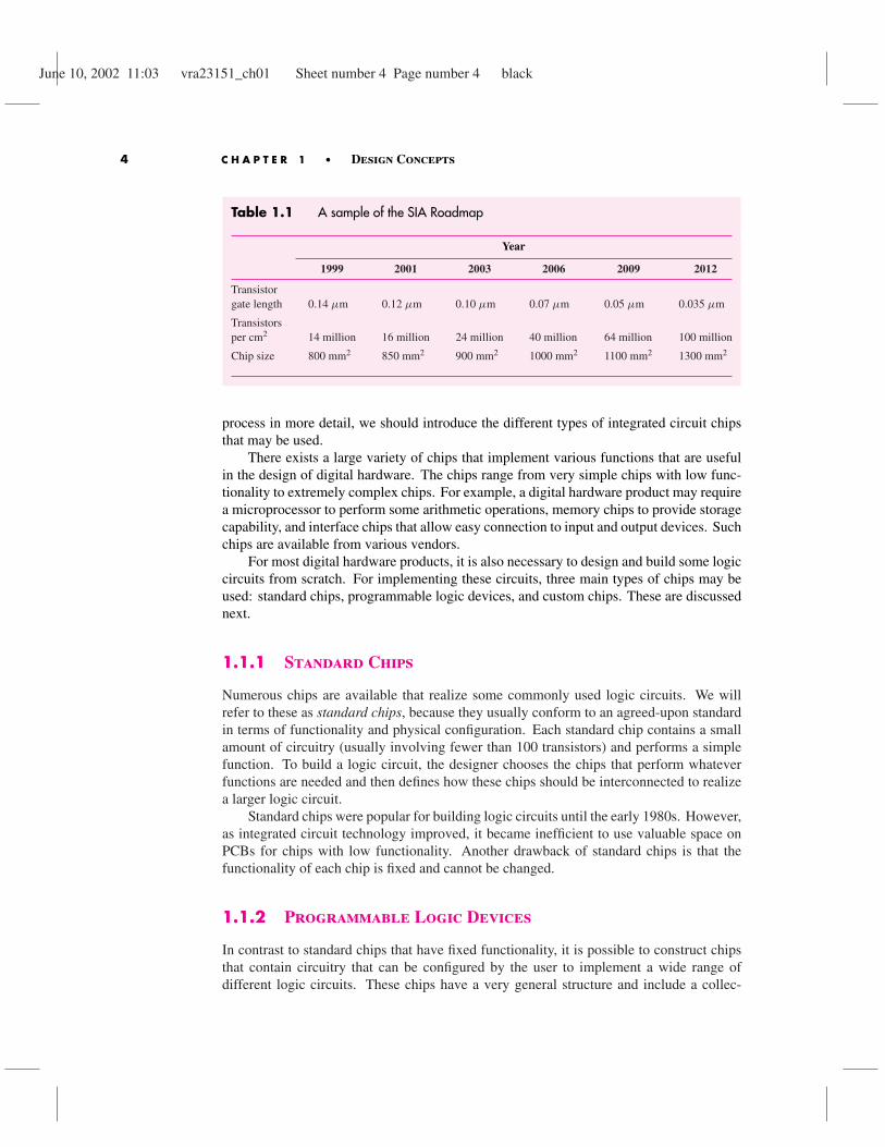
Moore’s law is expected to continue to hold true for at least the next decade. A con-sortium of integrated circuit manufacturers called the Semiconductor Industry Association(SIA) produces an estimate of how the technology is expected to evolve. Known as the SIARoadmap [1], this estimate predicts the minimum size of a transistor that can be fabricatedon an integrated circuit chip. The size of a transistor is measured by a parameter called itsgate length, which we will discuss in Chapter 3. A sample of the SIA Roadmap is given inTable 1.1. In 2002 the minimum possible gate length that can be reliably manufactured is0.13 µm. The first row of the table indicates that the minimum gate length is expected toreduce steadily to about 0.035 µm by the year 2012. The size of a transistor determines howmany transistors can be placed in a given amount of chip area, with the current maximumbeing about 20 million transistors per cm2. This number is expected to grow to 100 milliontransistors by the year 2012. The largest chip size is expected to be about 1300 mm2 at thattime; thus chips with up to 1.3 billion transistors will be possible! There is no doubt thatthis technology will have a huge impact on all aspects of people’s lives.
The designer of digital hardware may be faced with designing logic circuits that can beimplemented on a single chip or, more likely, designing circuits that involve a number ofchips placed on a printed circuit board (PCB). Frequently, some of the logic circuits can berealized in existing chips that are readily available. This situation simplifies the design taskand shortens the time needed to develop the final product. Before we discuss the design
June 10, 2002 11:03 vra23151_ch01 Sheet number 4 Page number 4 black
4 C H A P T E R 1 • Design Concepts
Table 1.1 A sample of the SIA Roadmap
Year
1999 2001 2003 2006 2009 2012
Transistorgate length 0.14 µm 0.12 µm 0.10 µm 0.07 µm 0.05 µm 0.035 µm
Transistorsper cm2 14 million 16 million 24 million 40 million 64 million 100 million
Chip size 800 mm2 850 mm2 900 mm2 1000 mm2 1100 mm2 1300 mm2
process in more detail, we should introduce the different types of integrated circuit chipsthat may be used.
There exists a large variety of chips that implement various functions that are usefulin the design of digital hardware. The chips range from very simple chips with low func-tionality to extremely complex chips. For example, a digital hardware product may requirea microprocessor to perform some arithmetic operations, memory chips to provide storagecapability, and interface chips that allow easy connection to input and output devices. Suchchips are available from various vendors.
For most digital hardware products, it is also necessary to design and build some logiccircuits from scratch. For implementing these circuits, three main types of chips may beused: standard chips, programmable logic devices, and custom chips. These are discussednext.
1.1.1 Standard Chips
Numerous chips are available that realize some commonly used logic circuits. We willrefer to these as standard chips, because they usually conform to an agreed-upon standardin terms of functionality and physical configuration. Each standard chip contains a smallamount of circuitry (usually involving fewer than 100 transistors) and performs a simplefunction. To build a logic circuit, the designer chooses the chips that perform whateverfunctions are needed and then defines how these chips should be interconnected to realizea larger logic circuit.
Standard chips were popular for building logic circuits until the early 1980s. However,as integrated circuit technology improved, it became inefficient to use valuable space onPCBs for chips with low functionality. Another drawback of standard chips is that thefunctionality of each chip is fixed and cannot be changed.
1.1.2 Programmable Logic Devices
In contrast to standard chips that have fixed functionality, it is possible to construct chipsthat contain circuitry that can be configured by the user to implement a wide range ofdifferent logic circuits. These chips have a very general structure and include a collec-

June 10, 2002 11:03 vra23151_ch01 Sheet number 5 Page number 5 black
1.1 Digital Hardware 5
Figure 1.2 A field-programmable gate array chip (courtesy ofAltera Corp.).
tion of programmable switches that allow the internal circuitry in the chip to be con-figured in many different ways. The designer can implement whatever functions areneeded for a particular application by choosing an appropriate configuration of the switches.The switches are programmed by the end user, rather than when the chip is manufactured.Such chips are known as programmable logic devices (PLDs). We will introduce them inChapter 3.
Most types of PLDs can be programmed multiple times. This capability is advantageousbecause a designer who is developing a prototype of a product can program a PLD to performsome function, but later, when the prototype hardware is being tested, can make correctionsby reprogramming the PLD. Reprogramming might be necessary, for instance, if a designedfunction is not quite as intended or if new functions are needed that were not contemplatedin the original design.
PLDs are available in a wide range of sizes. They can be used to realize much largerlogic circuits than a typical standard chip can realize. Because of their size and the fact thatthey can be tailored to meet the requirements of a specific application, PLDs are widelyused today. One of the most sophisticated types of PLD is known as a field-programmablegate array (FPGA). FPGAs that contain more than 100 million transistors are now available[2, 3]. A photograph of an FPGA chip that has 10 million transistors is shown in Figure 1.2.The chip consists of a large number of small logic circuit elements, which can be connectedtogether using the programmable switches. The logic circuit elements are arranged in aregular two-dimensional structure.
1.1.3 Custom-Designed Chips
PLDs are available as off-the-shelf components that can be purchased from different sup-pliers. Because they are programmable, they can be used to implement most logic circuitsfound in digital hardwaÌe. However, PLDs also have a drawback in that the programmableswitches consume valuable chip area and limit the speed of operation of implemented cir-

June 10, 2002 11:03 vra23151_ch01 Sheet number 6 Page number 6 black
6 C H A P T E R 1 • Design Concepts
cuits. Thus in some cases PLDs may not meet the desired performance or cost objectives.In such situations it is possible to design a chip from scratch; namely, the logic circuitrythat must be included on the chip is designed first and then an appropriate technology ischosen to implement the chip. Finally, the chip is manufactured by a company that has thefabrication facilities. This approach is known as custom or semi-custom design, and suchchips are called custom or semi-custom chips. Such chips are intended for use in specificapplications and are sometimes called application-specific integrated circuits (ASICs).
The main advantage of a custom chip is that its design can be optimized for a specifictask; hence it usually leads to better performance. It is possible to include a larger amountof logic circuitry in a custom chip than would be possible in other types of chips. Thecost of producing such chips is high, but if they are used in a product that is sold in largequantities, then the cost per chip, amortized over the total number of chips fabricated, maybe lower than the total cost of off-the-shelf chips that would be needed to implement thesame function(s). Moreover, if a single chip can be used instead of multiple chips to achievethe same goal, then a smaller area is needed on a PCB that houses the chips in the finalproduct. This results in a further reduction in cost.
A disadvantage of the custom-design approach is that manufacturing a custom chipoften takes a considerable amount of time, on the order of months. In contrast, if a PLDcan be used instead, then the chips are programmed by the end user and no manufacturingdelays are involved.
1.2 The Design Process
The availability of computer-based tools has greatly influenced the design process in a widevariety of design environments. For example, designing an automobile is similar in thegeneral approach to designing a furnace or a computer. Certain steps in the developmentcycle must be performed if the final product is to meet the specified objectives. We willstart by introducing a typical development cycle in the most general terms. Then we willfocus on the particular aspects that pertain to the design of logic circuits.
The flowchart in Figure 1.3 depicts a typical development process. We assume thatthe process is to develop a product that meets certain expectations. The most obviousrequirements are that the product must function properly, that it must meet an expectedlevel of performance, and that its cost should not exceed a given target.
The process begins with the definition of product specifications. The essential featuresof the product are identified, and an acceptable method of evaluating the implementedfeatures in the final product is established. The specifications must be tight enough toensure that the developed product will meet the general expectations, but should not beunnecessarily constraining (that is, the specifications should not prevent design choicesthat may lead to unforeseen advantages).
From a complete set of specifications, it is necessary to define the general structure ofan initial design of the product. This step is difficult to automate. It is usually performed bya human designer because there is no clear-cut strategy for developing a product’s overallstructure—it requires considerable design experience and intuition.
After the general structure is established, CAD tools are used to work out the details.Many types of CAD tools are available, ranging from those that help with the design

June 10, 2002 11:03 vra23151_ch01 Sheet number 7 Page number 7 black
1.2 The Design Process 7
Required product
Define specifications
Initial design
Simulation
Design correct?
Redesign
Prototype implementation
Testing
Meets specifications?
Finished product
Minor errors?
Make corrections
No
Yes
No
Yes
Yes
No
Figure 1.3 The development process.
of individual parts of the system to those that allow the entire system’s structure to berepresented in a computer. When the initial design is finished, the results must be verifiedagainst the original specifications. Traditionally, before the advent of CAD tools, this stepinvolved constructing a physical model of the designed product, usually including just thekey parts. Today it is seldom necessary to build a physical model. CAD tools enable

June 10, 2002 11:03 vra23151_ch01 Sheet number 8 Page number 8 black
8 C H A P T E R 1 • Design Concepts
designers to simulate the behavior of incredibly complex products, and such simulationsare used to determine whether the obtained design meets the required specifications. Iferrors are found, then appropriate changes are made and the verification of the new designis repeated through simulation. Although some design flaws may escape detection viasimulation, usually all but the most subtle problems are discovered in this way.
When the simulation indicates that the design is correct, a complete physical prototypeof the product is constructed. The prototype is thoroughly tested for conformance with thespecifications. Any errors revealed in the testing must be fixed. The errors may be minor,and often they can be eliminated by making small corrections directly on the prototype ofthe product. In case of large errors, it is necessary to redesign the product and repeat thesteps explained above. When the prototype passes all the tests, then the product is deemedto be successfully designed and it can go into production.
1.3 Design of Digital Hardware
Our previous discussion of the development process is relevant in a most general way. Thesteps outlined in Figure 1.3 are fully applicable in the development of digital hardware.Before we discuss the complete sequence of steps in this development environment, weshould emphasize the iterative nature of the design process.
1.3.1 Basic Design Loop
Any design process comprises a basic sequence of tasks that are performed in varioussituations. This sequence is presented in Figure 1.4. Assuming that we have an initialconcept about what should be achieved in the design process, the first step is to generatean initial design. This step often requires a lot of manual effort because most designs havesome specific goals that can be reached only through the designer’s knowledge, skill, andintuition. The next step is the simulation of the design at hand. There exist excellentCAD tools to assist in this step. To carry out the simulation successfully, it is necessaryto have adequate input conditions that can be applied to the design that is being simulatedand later to the final product that has to be tested. Applying these input conditions, thesimulator tries to verify that the designed product will perform as required under the orig-inal product specifications. If the simulation reveals some errors, then the design mustbe changed to overcome the problems. The redesigned version is again simulated to de-termine whether the errors have disappeared. This loop is repeated until the simulationindicates a successful design. A prudent designer expends considerable effort to remedyerrors during simulation because errors are typically much harder to fix if they are dis-covered late in the design process. Even so, some errors may not be detected duringsimulation, in which case they have to be dealt with in later stages of the developmentcycle.

June 10, 2002 11:03 vra23151_ch01 Sheet number 9 Page number 9 black
1.3 Design of Digital Hardware 9
Design concept
Successful design
Initial design
Simulation
Design correct?
Redesign
No
Yes
Figure 1.4 The basic design loop.
1.3.2 Design of a Digital Hardware Unit
Digital hardware products usually involve one or more PCBs that contain many chips andother components. Development of such products starts with the definition of the overallstructure. Then the required integrated circuit chips are selected, and the PCBs that houseand connect the chips together are designed. If the selected chips include PLDs or customchips, then these chips must be designed before the PCB-level design is undertaken. Sincethe complexity of circuits implemented on individual chips and on the circuit boards isusually very high, it is essential to make use of good CAD tools.
An example of a PCB is given in Figure 1.5. The PCB is a part of a large computersystem designed at the University of Toronto. This computer, called NUMAchine [4,5], isa multiprocessor, which means that it contains many processors that can be used togetherto work on a particular task. The PCB in the figure contains one processor chip and variousmemory and support chips. Complex logic circuits are needed to form the interface betweenthe processor and the rest of the system. A number of PLDs are used to implement theselogic circuits.
To illustrate the complete development cycle in more detail, we will consider the stepsneeded to produce a digital hardware unit that can be implemented on a PCB. This hardware

June 10, 2002 11:03 vra23151_ch01 Sheet number 10 Page number 10 black
10 C H A P T E R 1 • Design Concepts
Figure 1.5 A printed circuit board.
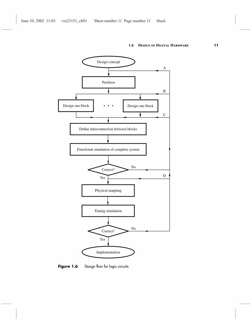
could be viewed as a very complex logic circuit that performs the functions defined by theproduct specifications. Figure 1.6 shows the design flow, assuming that we have a designconcept that defines the expected behavior and characteristics of this large circuit.
An orderly way of dealing with the complexity involved is to partition the circuit intosmaller blocks and then to design each block separately. Breaking down a large task intomore manageable smaller parts is known as the divide-and-conquer approach. The designof each block follows the procedure outlined in Figure 1.4. The circuitry in each block isdefined, and the chips needed to implement it are chosen. The operation of this circuitry issimulated, and any necessary corrections are made.
Having successfully designed all blocks, the interconnection between the blocks mustbe defined, which effectively combines these blocks into a single large circuit. Now itis necessary to simulate this complete circuit and correct any errors. Depending on theerrors encountered, it may be necessary to go back to the previous steps as indicated by thepaths A, B, and C in the flowchart. Some errors may be caused by incorrect connections
June 10, 2002 11:03 vra23151_ch01 Sheet number 11 Page number 11 black
1.3 Design of Digital Hardware 11
Define interconnection between blocks
Functional simulation of complete system
Correct?
Physical mapping
Timing simulation
Correct?
Implementation
No
Yes
No
Yes
Design one block Design one block
Partition
Design concept
A
B
C
D
Figure 1.6 Design flow for logic circuits.

June 10, 2002 11:03 vra23151_ch01 Sheet number 12 Page number 12 black
12 C H A P T E R 1 • Design Concepts
between the blocks, in which case these connections have to be redefined, following path C.Some blocks may not have been designed correctly, in which case path B is followed and theerroneous blocks are redesigned. Another possibility is that the very first step of partitioningthe overall large circuit into blocks was not done well, in which case path A is followed.This may happen, for example, if none of the blocks implement some functionality neededin the complete circuit.
Successful completion of functional simulation suggests that the designed circuit willcorrectly perform all of its functions. The next step is to decide how to realize this circuiton a PCB. The physical location of each chip on the board has to be determined, and thewiring pattern needed to make connections between the chips has to be defined. We referto this step as the physical design of the PCB. CAD tools are relied on heavily to performthis task automatically.
Once the placement of chips and the actual wire connections on the PCB have beenestablished, it is desirable to see how this physical layout will affect the performance ofthe circuit on the finished board. It is reasonable to assume that if the previous functionalsimulation indicated that all functions will be performed correctly, then the CAD toolsused in the physical design step will ensure that the required functional behavior will notbe corrupted by placing the chips on the board and wiring them together to realize thefinal circuit. However, even though the functional behavior may be correct, the realizedcircuit may operate more slowly than desired and thus lead to inadequate performance. Thiscondition occurs because the physical wiring on the PCB involves metal traces that presentresistance and capacitance to electrical signals and thus may have a significant impact on thespeed of operation. To distinguish between simulation that considers only the functionalityof the circuit and simulation that also considers timing behavior, it is customary to usethe terms functional simulation and timing simulation. A timing simulation may revealpotential performance problems, which can then be corrected by using the CAD tools tomake changes in the physical design of the PCB.
Having completed the design process, the designed circuit is ready for physical im-plementation. The steps needed to implement a prototype board are indicated in Figure1.7. A first version of the board is built and tested. Most minor errors that are detected canusually be corrected by making changes directly on the prototype board. This may involvechanges in wiring or perhaps reprogramming some PLDs. Larger problems require a moresubstantial redesign. Depending on the nature of the problem, the designer may have toreturn to any of the points A, B, C, or D in the design process of Figure 1.6.
We have described the development process where the final circuit is implementedusing many chips on a PCB. The material presented in this book is directly applicable tothis type of design problem. However, for practical reasons the design examples that appearin the book are relatively small and can be realized in a single integrated circuit, either acustom-designed chip or a PLD. All the steps in Figure 1.6 are relevant in this case as well,with the understanding that the circuit blocks to be designed are on a smaller scale.
1.4 Logic Circuit Design in This Book
In this book we use PLDs extensively to illustrate many aspects of logic circuit design.We selected this technology because it is widely used in real digital hardware products

June 10, 2002 11:03 vra23151_ch01 Sheet number 13 Page number 13 black
1.4 Logic Circuit Design in This Book 13
Implementation
Finished PCB
Build prototype
Testing
Correct?
Modify prototype
No
Yes
Minor errors?
Yes
Go to A, B, C, or D in Figure 1.6
No
Figure 1.7 Completion of PCB development.
and because the chips are user programmable. PLD technology is particularly well suitedfor educational purposes because many readers have access to facilities for programmingPLDs, which enables the reader to actually implement the sample circuits. To illustratepractical design issues, in this book we use two types of PLDs—they are the two typesof devices that are widely used in digital hardware products today. One type is known ascomplex programmable logic devices (CPLDs) and the other as field-programmable gatearrays (FPGAs). These chips are introduced in Chapter 3.
To gain practical experience and a deeper understanding of logic circuits, we advise thereader to implement the examples in this book using CAD tools. Most of the major vendorsof CAD systems provide their tools through university programs for educational use. Someexamples are Altera, Cadence, Mentor Graphics, Synopsys, Synplicity, and Xilinx. TheCAD systems offered by any of these companies can be used equally well with this book.For those who do not already have access to CAD tools, we include Altera’s MAX+plusIICAD system on a CD-ROM. This industrial-quality software supports all phases of thedesign cycle and is powerful and easy to use. The software is easily installed on a personalcomputer, and we provide a sequence of complete step-by-step tutorials in Appendices B,C, and D to illustrate the use of CAD tools in concert with the book.
For educational purposes, some PLD manufacturers provide laboratory developmentprinted circuit boards that include one or more PLD chips and an interface to a personalcomputer. Once a logic circuit has been designed using the CAD tools, the circuit can be

June 10, 2002 11:03 vra23151_ch01 Sheet number 14 Page number 14 black
14 C H A P T E R 1 • Design Concepts
downloaded into a PLD on the board. Inputs can then be applied to the PLD by way ofsimple switches, and the generated outputs can be examined. These laboratory boards aredescribed on the World Wide Web pages of the PLD suppliers.
1.5 Theory and Practice
Modern design of logic circuits depends heavily on CAD tools, but the discipline of logicdesign evolved long before CAD tools were invented. This chronology is quite obviousbecause the very first computers were built with logic circuits, and there certainly were nocomputers available on which to design them!
Numerous manual design techniques have been developed to deal with logic circuits.Boolean algebra, which we will introduce in Chapter 2, was adopted as a mathematicalmeans for representing such circuits. An enormous amount of “theory” was developed,showing how certain design issues may be treated. To be successful, a designer had toapply this knowledge in practice.
CAD tools not only made it possible to design incredibly complex circuits but alsomade the design work much simpler in general. They perform many tasks automatically,which may suggest that today’s designer need not understand the theoretical concepts usedin the tasks performed by CAD tools. An obvious question would then be, Why should onestudy the theory that is no longer needed for manual design? Why not simply learn how touse the CAD tools?
There are three big reasons for learning the relevant theory. First, although the CADtools perform the automatic tasks of optimizing a logic circuit to meet particular designobjectives, the designer has to give the original description of the logic circuit. If thedesigner specifies a circuit that has inherently bad properties, then the final circuit will alsobe of poor quality. Second, the algebraic rules and theorems for design and manipulationof logic circuits are directly implemented in today’s CAD tools. It is not possible for a userof the tools to understand what the tools do without grasping the underlying theory. Third,CAD tools offer many optional processing steps that a user can invoke when working ona design. The designer chooses which options to use by examining the resulting circuitproduced by the CAD tools and deciding whether it meets the required objectives. Theonly way that the designer can know whether or not to apply a particular option in a givensituation is to know what the CAD tools will do if that option is invoked—again, this impliesthat the designer must be familiar with the underlying theory. We discuss the classical logiccircuit theory extensively in this book, because it is not possible to become an effectivelogic circuit designer without understanding the fundamental concepts.
On a final note, there is another good reason to learn some logic circuit theory even if itwere not required for CAD tools. Simply put, it is interesting and intellectually challenging.In the modern world filled with sophisticated automatic machinery, it is tempting to rely ontools as a substitute for thinking. However, in logic circuit design, as in any type of designprocess, computer-based tools are not a substitute for human intuition and innovation.Computer-based tools can produce good digital hardware designs only when employed bya designer who thoroughly understands the nature of logic circuits.

June 10, 2002 11:03 vra23151_ch01 Sheet number 15 Page number 15 black
References 15
References
1. Semiconductor Industry Association, “National Technology Roadmap for Semi-conductors,” http://www.semichips.org/
2. Altera Corporation, “APEX II Programmable Logic Devices,” http://www.altera.com
3. Xilinx Corporation, “Virtex II Field Programmable Gate Arrays,”http://www.xilinx.com
4. S. Brown, N. Manjikian, Z. Vranesic, S. Caranci, A. Grbic, R. Grindley, M. Gusat,K. Loveless, Z. Zilic, and S. Srbljic, “Experience in Designing a Large-ScaleMultiprocessor Using Field-Programmable Devices and Advanced CAD Tools,” 33rdIEEE Design Automation Conference, Las Vegas, June 1996.
5. A. Grbic, S. Brown, S. Caranci, R. Grindley, M. Gusat, G. Lemieux, K. Loveless,N. Manjikian, S. Srbljic, M. Stumm, Z. Vranesic, and Z. Zilic, “ The Design andImplementation of the NUMAchine Multiprocessor,” IEEE Design AutomationConference, San Francisco, June 1998.


