39
Designing VLSI Interconnects with Monolithically Integrated Silicon-Photonics Vladimir Stojanović MIT SSCS DL series – Santa Clara, CA, November, 2012
Designing VLSI Interconnects
with Monolithically Integrated
Silicon-Photonics
Vladimir Stojanović
MIT
SSCS DL series – Santa Clara, CA, November, 2012
Acknowledgments
• Rajeev Ram, Henry Smith, Hanqing Li (MIT), Milos Popović (Boulder),
Krste Asanović (UC Berkeley)
• Jason Orcutt, Jeffrey Shainline, Christopher Batten, Ajay Joshi, Anatoly
Khilo
• Karan Mehta, Mark Wade, Erman Timurdogan, Stevan Urosevic, Jie Sun,
Cheryl Sorace, Josh Wang
• Michael Georgas, Jonathan Leu, Benjamin Moss, Chen Sun
• Yong-Jin Kwon, Scott Beamer, Yunsup Lee, Andrew Waterman, Miquel
Planas
• DARPA, NSF and FCRP IFC
• IBM Trusted Foundry, Solid-State Circuits Society
2
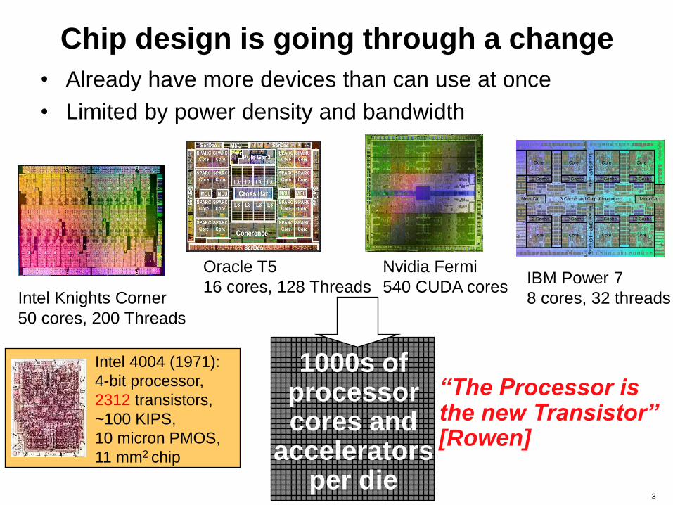
Chip design is going through a change
• Already have more devices than can use at once
• Limited by power density and bandwidth
“The Processor is the new Transistor” [Rowen]
Intel 4004 (1971):
4-bit processor,
2312 transistors,
~100 KIPS,
10 micron PMOS,
11 mm2 chip
1000s of processor cores and
accelerators per die
Intel Knights Corner
50 cores, 200 Threads
Oracle T5
16 cores, 128 Threads
Nvidia Fermi
540 CUDA cores IBM Power 7
8 cores, 32 threads
3
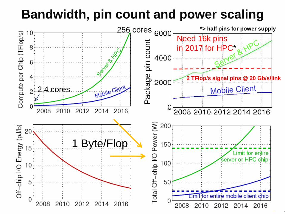
Bandwidth, pin count and power scaling
Need 16k pins
in 2017 for HPC*
1 Byte/Flop
256 cores
2 TFlop/s signal pins @ 20 Gb/s/link
2,4 cores
Pa
cka
ge
pin
co
un
t
*> half pins for power supply
• 4
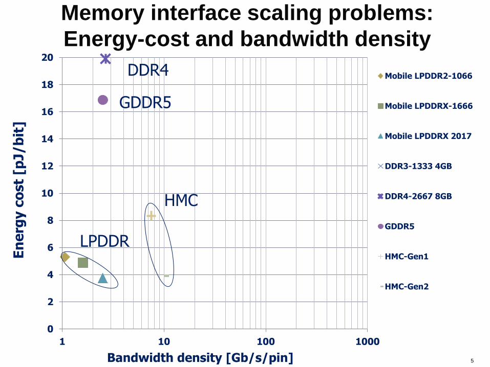
0
2
4
6
8
10
12
14
16
18
20
1 10 100 1000
Mobile LPDDR2-1066
Mobile LPDDRX-1666
Mobile LPDDRX 2017
DDR3-1333 4GB
DDR4-2667 8GB
GDDR5
HMC-Gen1
HMC-Gen2
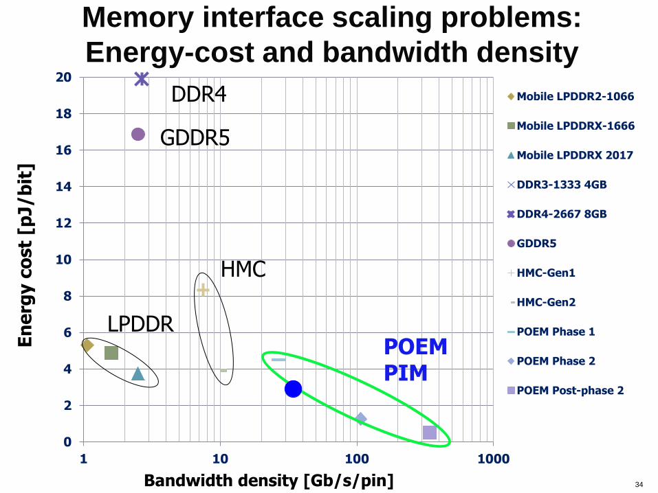
Memory interface scaling problems:
Energy-cost and bandwidth density
HMC
LPDDR
En
erg
y c
ost
[pJ/b
it]
Bandwidth density [Gb/s/pin]
DDR4
GDDR5
5
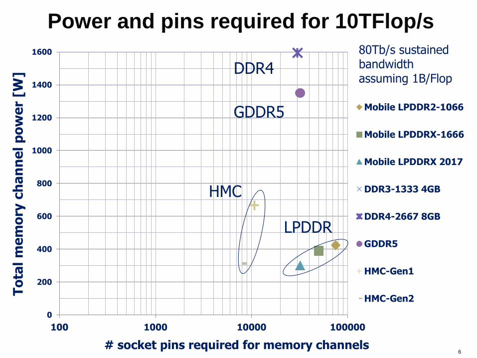
Power and pins required for 10TFlop/s
0
200
400
600
800
1000
1200
1400
1600
100 1000 10000 100000
Mobile LPDDR2-1066
Mobile LPDDRX-1666
Mobile LPDDRX 2017
DDR3-1333 4GB
DDR4-2667 8GB
GDDR5
HMC-Gen1
HMC-Gen2 To
tal
me
mo
ry c
ha
nn
el p
ow
er
[W]
# socket pins required for memory channels
80Tb/s sustained bandwidth assuming 1B/Flop
HMC
LPDDR
DDR4
GDDR5
6
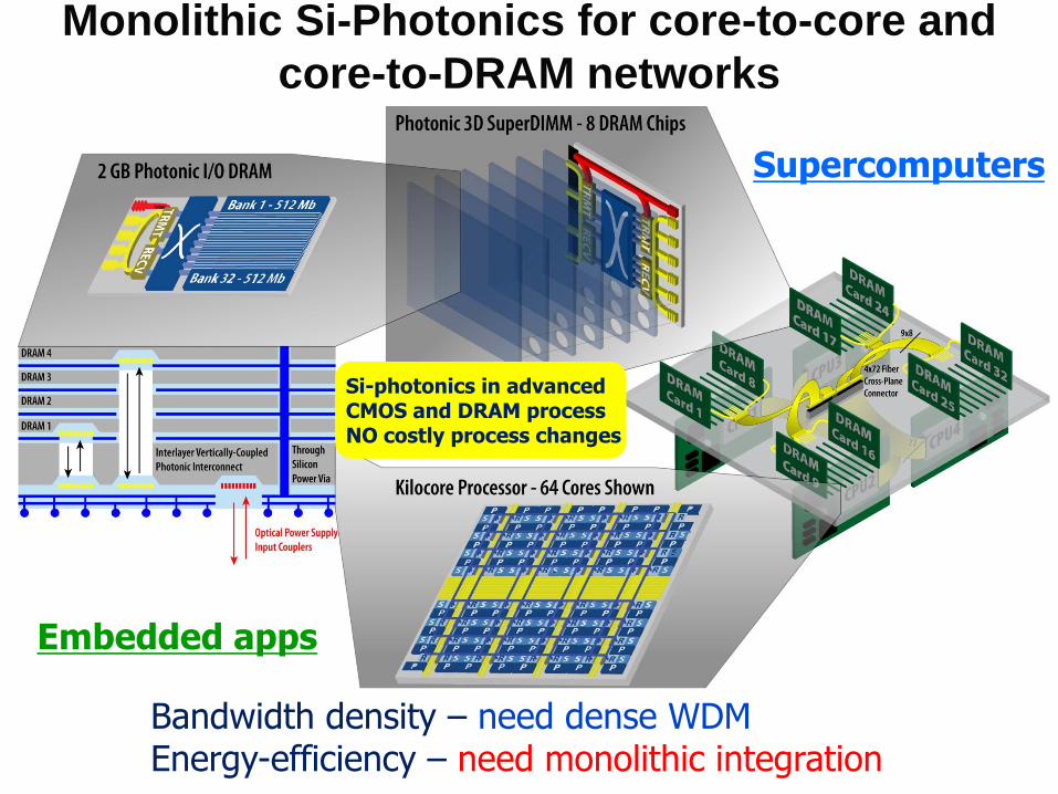
Monolithic Si-Photonics for core-to-core and
core-to-DRAM networks
7 7
Supercomputers
Embedded apps
Si-photonics in advanced CMOS and DRAM process NO costly process changes
Bandwidth density – need dense WDM Energy-efficiency – need monolithic integration
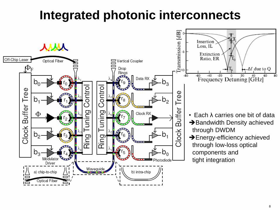
Integrated photonic interconnects
• Each λ carries one bit of data
Bandwidth Density achieved
through DWDM
Energy-efficiency achieved
through low-loss optical
components and
tight integration
8
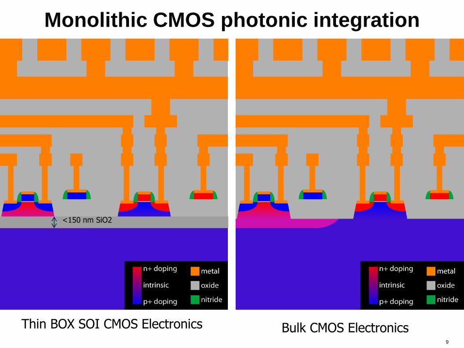
Thin BOX SOI CMOS Electronics
Bulk CMOS Electronics
<150 nm SiO2
Monolithic CMOS photonic integration
9
9
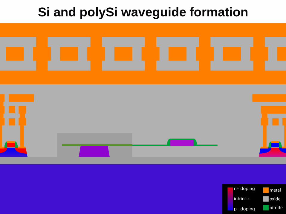
Si and polySi waveguide formation
10
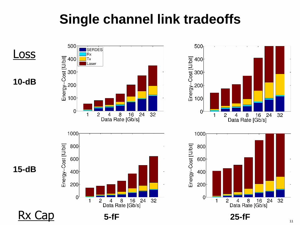
Single channel link tradeoffs
10-dB
15-dB
Loss
5-fF 25-fF Rx Cap 11
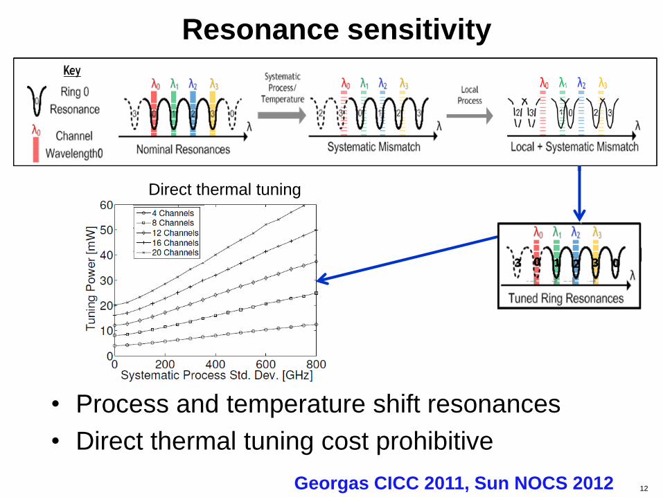
Resonance sensitivity
• Process and temperature shift resonances
• Direct thermal tuning cost prohibitive
Direct thermal tuning
Georgas CICC 2011, Sun NOCS 2012 12
0 1 2 3 3 0
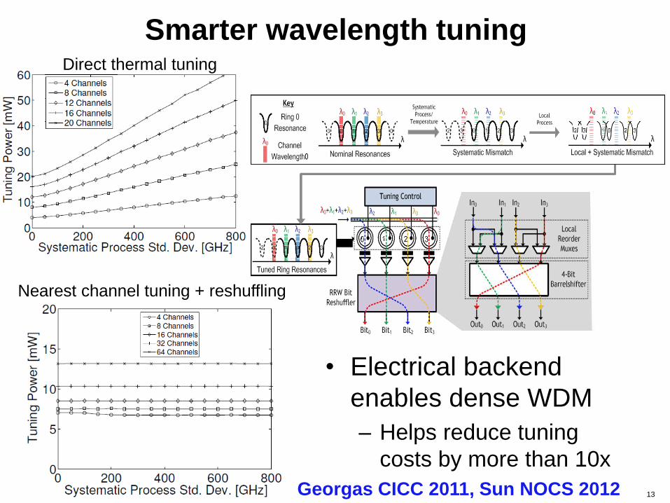
Smarter wavelength tuning
• Electrical backend
enables dense WDM
– Helps reduce tuning
costs by more than 10x
Direct thermal tuning
Nearest channel tuning + reshuffling
Georgas CICC 2011, Sun NOCS 2012 13
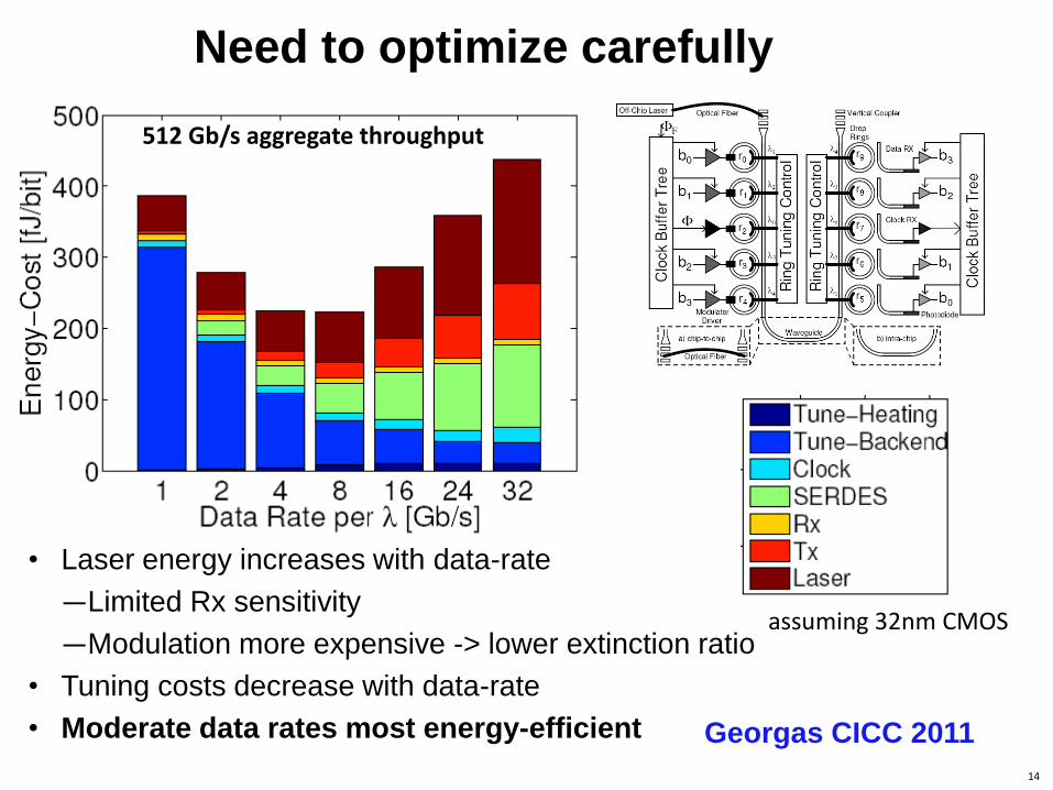
14
• Laser energy increases with data-rate
—Limited Rx sensitivity
—Modulation more expensive -> lower extinction ratio
• Tuning costs decrease with data-rate
• Moderate data rates most energy-efficient
512 Gb/s aggregate throughput
assuming 32nm CMOS
Georgas CICC 2011
Need to optimize carefully
15
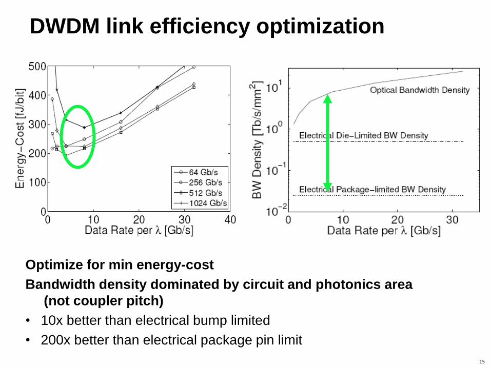
DWDM link efficiency optimization
Optimize for min energy-cost
Bandwidth density dominated by circuit and photonics area
(not coupler pitch)
• 10x better than electrical bump limited
• 200x better than electrical package pin limit
16
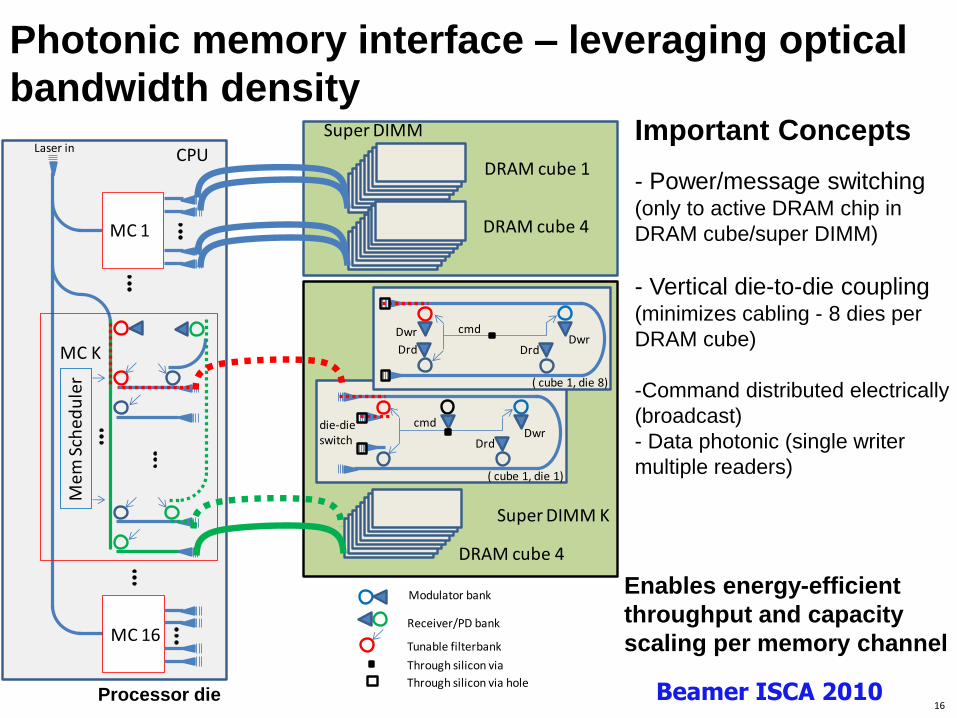
Photonic memory interface – leveraging optical
bandwidth density Important Concepts
- Power/message switching (only to active DRAM chip in
DRAM cube/super DIMM)
- Vertical die-to-die coupling (minimizes cabling - 8 dies per
DRAM cube)
-Command distributed electrically
(broadcast)
- Data photonic (single writer
multiple readers)
MC 1
MC 16
Mem
Sch
edu
ler
MC K
CPUDRAM cube 1
DRAM cube 4
Super DIMM
cmdDwr
Drd
( cube 1, die 1)
cmdDwr
Drd
( cube 1, die 8)
Dwr
Drd
DRAM cube 4
Super DIMM K
die-die switch
Laser in
Modulator bank
Receiver/PD bank
Tunable filterbank
Through silicon via
Through silicon via holeBeamer ISCA 2010 Processor die
Enables energy-efficient
throughput and capacity
scaling per memory channel
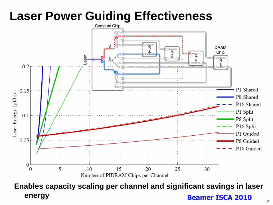
17
Enables capacity scaling per channel and significant savings in laser
energy
Laser Power Guiding Effectiveness
Beamer ISCA 2010
18
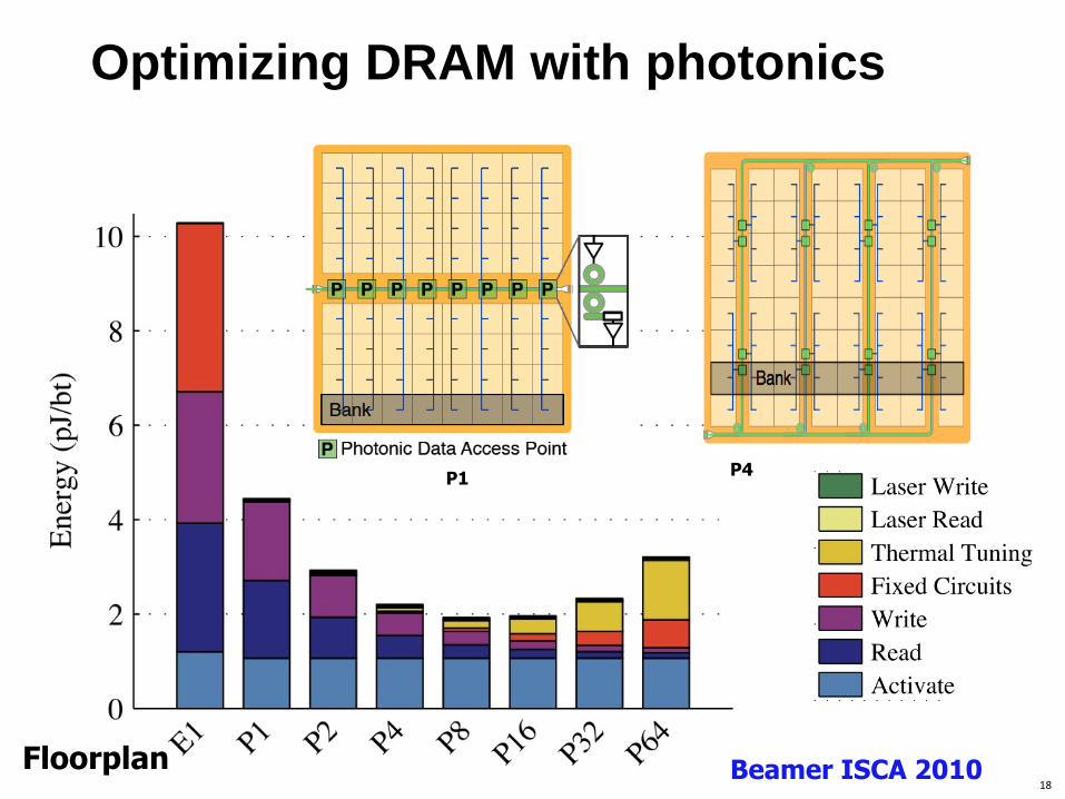
Optimizing DRAM with photonics
Floorplan
P1 P4
Beamer ISCA 2010
19
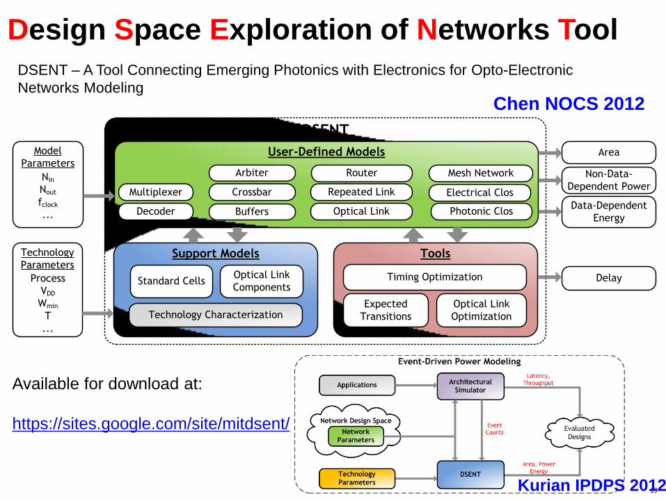
Design Space Exploration of Networks Tool
DSENT
User-Defined Models
Support Models Tools
Arbiter Router
Decoder Buffers
Technology Characterization
Area
Mesh Network
Electrical ClosRepeated Link
Optical Link Photonic Clos
CrossbarMultiplexer
Delay
Technology
Parameters
Model
Parameters
Standard Cells Timing Optimization
Expected
Transitions
Optical Link
Components
Optical Link
Optimization
Non-Data-
Dependent Power
Data-Dependent
Energy
Nin
Nout
fclock
...
Process
VDD
Wmin
T
...
19
DSENT – A Tool Connecting Emerging Photonics with Electronics for Opto-Electronic
Networks Modeling Chen NOCS 2012
Kurian IPDPS 2012
Available for download at:
https://sites.google.com/site/mitdsent/
20
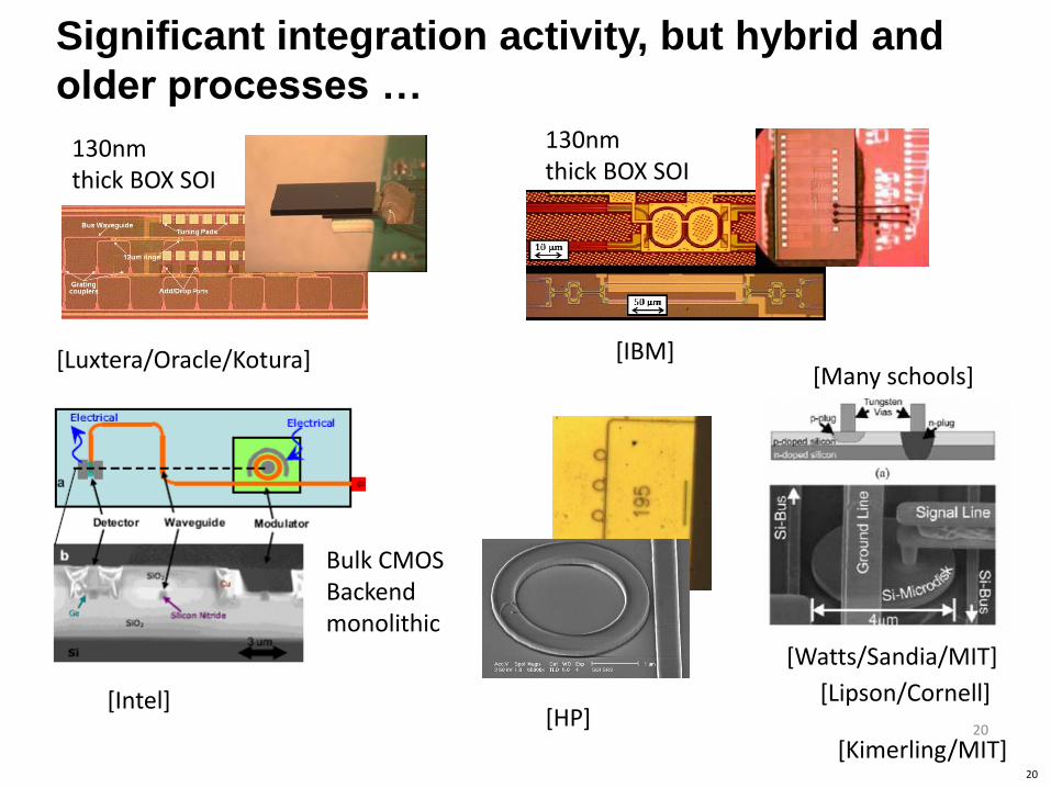
Significant integration activity, but hybrid and
older processes …
[Luxtera/Oracle/Kotura] [IBM]
[HP]
[Watts/Sandia/MIT]
[Intel]
130nm thick BOX SOI
130nm thick BOX SOI
Bulk CMOS Backend monolithic
[Lipson/Cornell]
[Kimerling/MIT]
[Many schools]
20
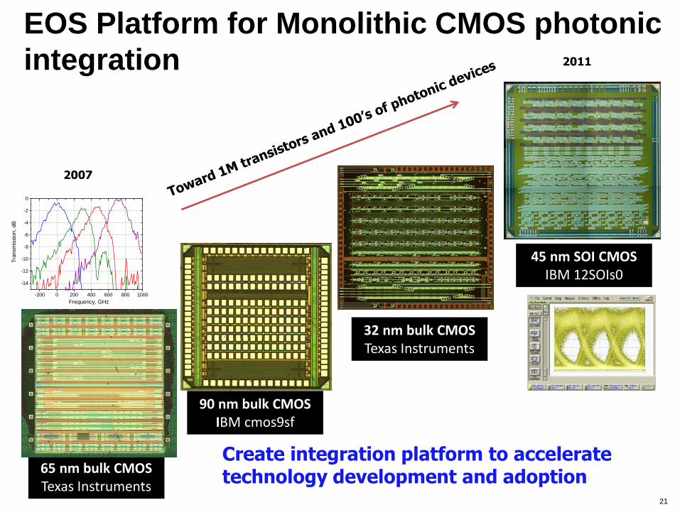
65 nm bulk CMOS Texas Instruments
90 nm bulk CMOS IBM cmos9sf
45 nm SOI CMOS IBM 12SOIs0
21
32 nm bulk CMOS Texas Instruments
EOS Platform for Monolithic CMOS photonic
integration
-200 0 200 400 600 800 1000
-14
-12
-10
-8
-6
-4
-2
0
Tra
nsm
issio
n, dB
Frequency, GHz
2007
2011
Create integration platform to accelerate technology development and adoption
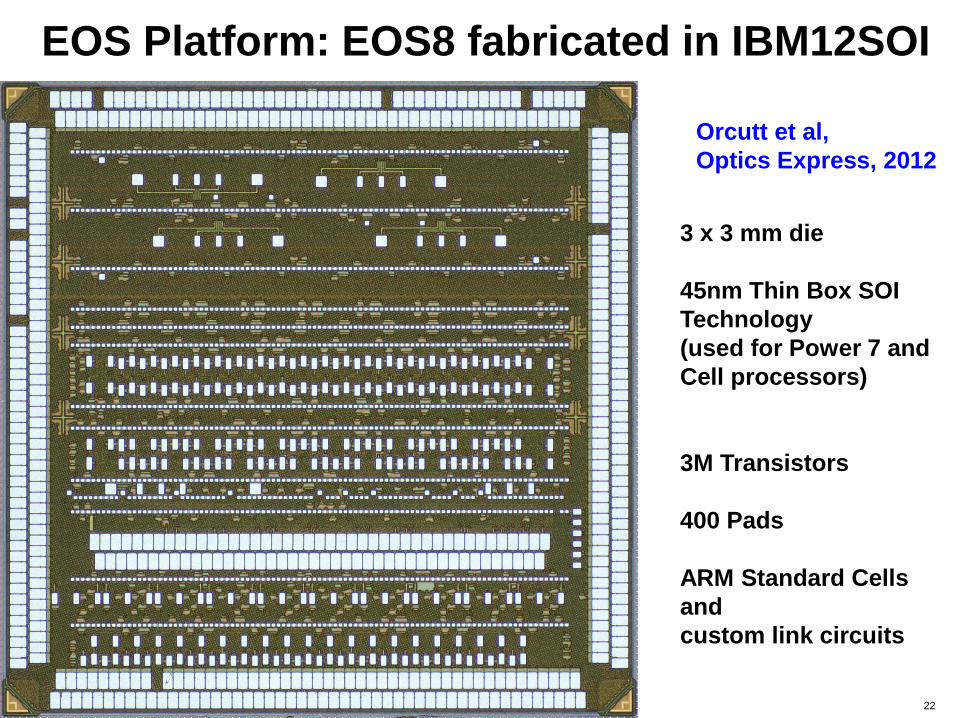
EOS Platform: EOS8 fabricated in IBM12SOI
3 x 3 mm die
45nm Thin Box SOI
Technology
(used for Power 7 and
Cell processors)
3M Transistors
400 Pads
ARM Standard Cells
and
custom link circuits
Orcutt et al,
Optics Express, 2012
22
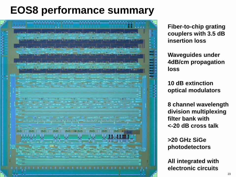
EOS8 performance summary
Fiber-to-chip grating
couplers with 3.5 dB
insertion loss
Waveguides under
4dB/cm propagation
loss
10 dB extinction
optical modulators
8 channel wavelength
division multiplexing
filter bank with
<-20 dB cross talk
>20 GHz SiGe
photodetectors
All integrated with
electronic circuits 23
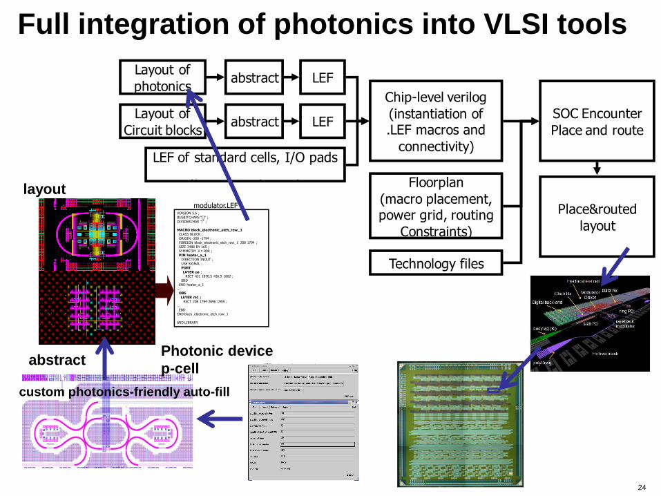
Full integration of photonics into VLSI tools
VERSION 5.6 ;
BUSBITCHARS "[]" ;
DIVIDERCHAR "/" ;
MACRO block_electronic_etch_row_1
CLASS BLOCK ;
ORIGIN -208 -1794 ;
FOREIGN block_electronic_etch_row_1 208 1794 ;
SIZE 2488 BY 165 ;
SYMMETRY X Y R90 ;
PIN heater_a_1
DIRECTION INOUT ;
USE SIGNAL ;
PORT
LAYER ua ;
RECT 431 1870.5 436.5 1882 ;
END
END heater_a_1
...
OBS
LAYER m1 ;
RECT 208 1794 2696 1959 ;
...
END
END block_electronic_etch_row_1
END LIBRARY
modulator.LEF
Layout of
photonics
Layout of
Circuit blocks
abstract
abstract
LEF
LEF
LEF of standard cells, I/O pads
(provided by ARM)
Chip-level verilog
(instantiation of.LEF macros and
connectivity)
Technology files
SOC Encounter
Place and route
Floorplan
(macro placement,power grid, routing
Constraints)
Place&routed
layout
Photonic device
p-cell abstract
custom photonics-friendly auto-fill
layout
24
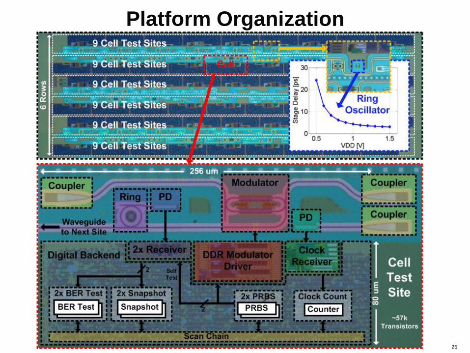
Platform Organization
25
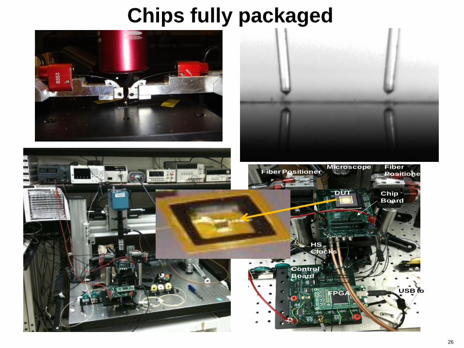
Chips fully packaged
DUT Chip
Board
HS
Clocks
FPGA
Control
Board
Fiber PositionerFiber
Positioner
USB to laptop
Microscope
26
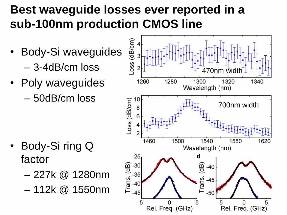
Best waveguide losses ever reported in a
sub-100nm production CMOS line
• Body-Si waveguides
– 3-4dB/cm loss
• Poly waveguides
– 50dB/cm loss
• Body-Si ring Q
factor
– 227k @ 1280nm
– 112k @ 1550nm
700nm width
470nm width
700nm width
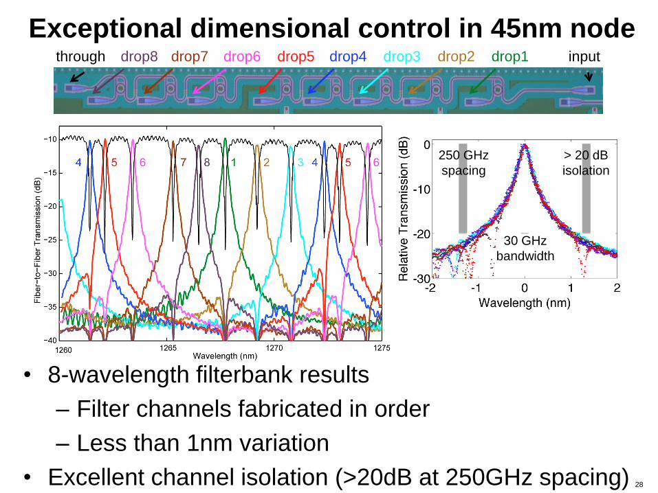
• 8-wavelength filterbank results
– Filter channels fabricated in order
– Less than 1nm variation
• Excellent channel isolation (>20dB at 250GHz spacing)
> 20 dB
isolation
30 GHz
bandwidth
250 GHz
spacing
through input drop8 drop7 drop6 drop5 drop4 drop3 drop2 drop1
Exceptional dimensional control in 45nm node
28
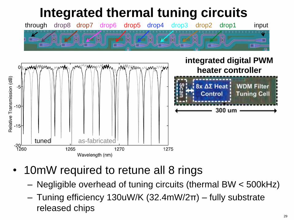
• 10mW required to retune all 8 rings
– Negligible overhead of tuning circuits (thermal BW < 500kHz)
– Tuning efficiency 130uW/K (32.4mW/2π) – fully substrate
released chips
tuned as-fabricated
integrated digital PWM
heater controller
through input drop8 drop7 drop6 drop5 drop4 drop3 drop2 drop1
Integrated thermal tuning circuits
29
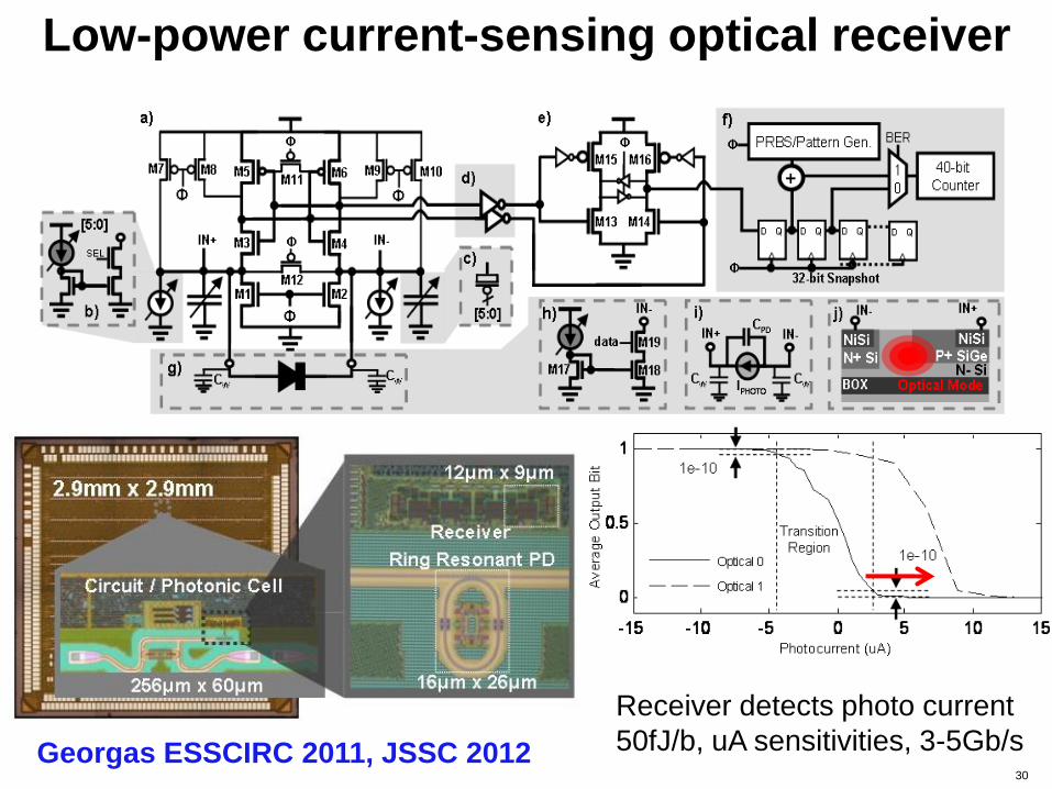
Low-power current-sensing optical receiver
Georgas ESSCIRC 2011, JSSC 2012
Receiver detects photo current
50fJ/b, uA sensitivities, 3-5Gb/s 30
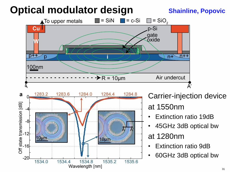
Optical modulator design
Carrier-injection device
at 1550nm
• Extinction ratio 19dB
• 45GHz 3dB optical bw
at 1280nm
• Extinction ratio 9dB
• 60GHz 3dB optical bw
Shainline, Popovic
31
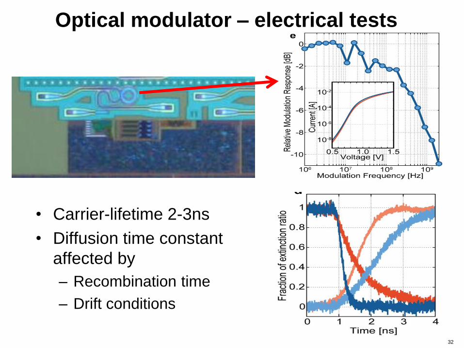
Optical modulator – electrical tests
• Carrier-lifetime 2-3ns
• Diffusion time constant
affected by
– Recombination time
– Drift conditions
32
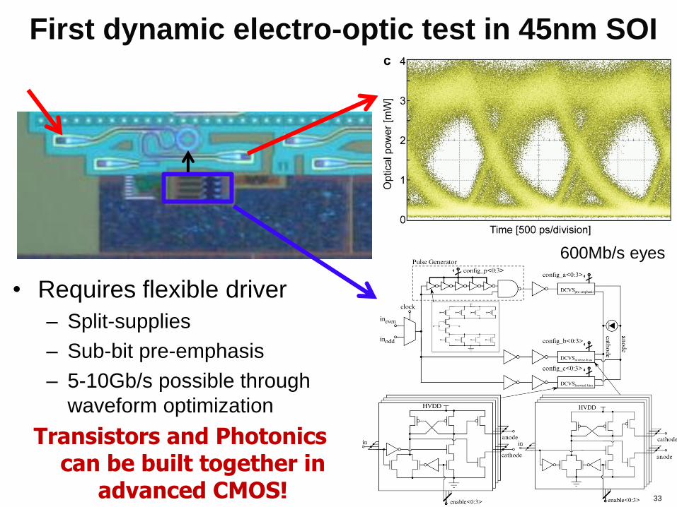
First dynamic electro-optic test in 45nm SOI
• Requires flexible driver
– Split-supplies
– Sub-bit pre-emphasis
– 5-10Gb/s possible through
waveform optimization
600Mb/s eyes
33
Transistors and Photonics can be built together in
advanced CMOS!
0
2
4
6
8
10
12
14
16
18
20
1 10 100 1000
Mobile LPDDR2-1066
Mobile LPDDRX-1666
Mobile LPDDRX 2017
DDR3-1333 4GB
DDR4-2667 8GB
GDDR5
HMC-Gen1
HMC-Gen2
POEM Phase 1
POEM Phase 2
POEM Post-phase 2
Memory interface scaling problems:
Energy-cost and bandwidth density
HMC
LPDDR
En
erg
y c
ost
[pJ/b
it]
Bandwidth density [Gb/s/pin]
DDR4
GDDR5
POEM PIM
34
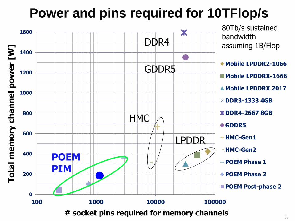
Power and pins required for 10TFlop/s
0
200
400
600
800
1000
1200
1400
1600
100 1000 10000 100000
Mobile LPDDR2-1066
Mobile LPDDRX-1666
Mobile LPDDRX 2017
DDR3-1333 4GB
DDR4-2667 8GB
GDDR5
HMC-Gen1
HMC-Gen2
POEM Phase 1
POEM Phase 2
POEM Post-phase 2
To
tal
me
mo
ry c
ha
nn
el p
ow
er
[W]
# socket pins required for memory channels
80Tb/s sustained bandwidth assuming 1B/Flop
HMC
LPDDR
POEM PIM
DDR4
GDDR5
35
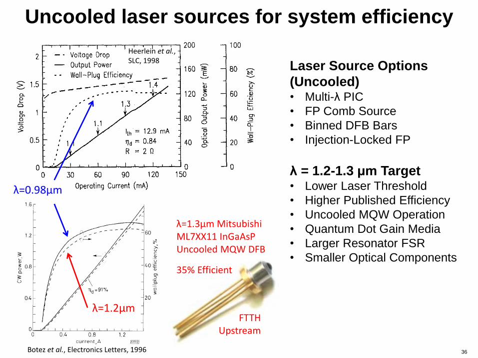
Uncooled laser sources for system efficiency
Laser Source Options
(Uncooled) • Multi-λ PIC
• FP Comb Source
• Binned DFB Bars
• Injection-Locked FP
λ = 1.2-1.3 μm Target • Lower Laser Threshold
• Higher Published Efficiency
• Uncooled MQW Operation
• Quantum Dot Gain Media
• Larger Resonator FSR
• Smaller Optical Components
Botez et al., Electronics Letters, 1996
Heerlein et al., SLC, 1998
λ=0.98μm
λ=1.2μm
λ=1.3μm Mitsubishi ML7XX11 InGaAsP Uncooled MQW DFB
35% Efficient
FTTH Upstream
36
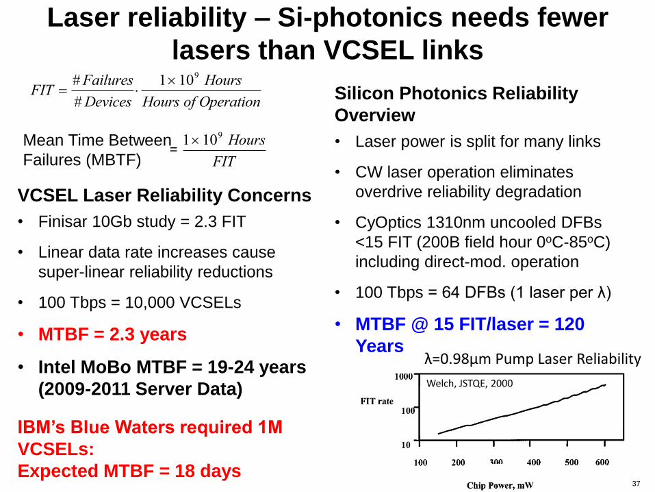
Laser reliability – Si-photonics needs fewer
lasers than VCSEL links
λ=0.98μm Pump Laser Reliability
Welch, JSTQE, 2000
VCSEL Laser Reliability Concerns
• Finisar 10Gb study = 2.3 FIT
• Linear data rate increases cause
super-linear reliability reductions
• 100 Tbps = 10,000 VCSELs
• MTBF = 2.3 years
• Intel MoBo MTBF = 19-24 years
(2009-2011 Server Data)
IBM’s Blue Waters required 1M
VCSELs:
Expected MTBF = 18 days
Silicon Photonics Reliability
Overview
• Laser power is split for many links
• CW laser operation eliminates
overdrive reliability degradation
• CyOptics 1310nm uncooled DFBs
<15 FIT (200B field hour 0oC-85oC)
including direct-mod. operation
• 100 Tbps = 64 DFBs (1 laser per λ)
• MTBF @ 15 FIT/laser = 120
Years
FIT #Failures
#Devices1109 Hours
Hours of Operation
1109 Hours
FIT
Mean Time Between
Failures (MBTF) =
37
electrical connections
Flip-chip mounted die
C4 bumps
Package substrate
Fiber ribbon
(100-200um pitch)
Front-side
Vertical couplers
electrical connections
Flip-chip mounted die
C4 bumps
Package substrate
Fiber ribbon
(100-200um pitch)
Front-side
Vertical couplers
• CPU package
– Flip-chip <5um C4
tolerance o.k. for
coupling
• DRAM package
– Die on board
– Connector-to-fiber
alignment <2um
Packaging
38
Summary
• Silicon-photonics can push both critical dimensions – Energy-efficiency – monolithic integration
– Bandwidth Density - dense WDM
• Need to optimize across layers – Connect devices to circuits, and links to networks
• Building early technology development platforms – Feedback to device and circuit designers
– Accelerated adoption
• EOS Platform designed for multi-project wafer runs – Best end-of-line passives in sub-100nm process (3-4dB/cm loss)
– 50 fJ/b receivers with uA sensitivities
– Record-high tuning efficiency with undercut ~ 25uW/K
– First modulation demonstrated in 45nm process
39


