Designing Wide Instantaneous Bandwidth Doherty PAs for CellularTim DasNXP, Chandler, Ariz.
The 3.5 GHz band is emerging as prime 4G and 5G spectral real estate around the globe. Radio interfaces are evolving through LTE-Advanced and LTE-Advanced Pro, raising the bar on base station power amplifier (PA) capability and performance. Instantaneous signal bandwidth is the key to a suitable solution. This article outlines the fundamentals of PA design for a symmetrical, wideband Doherty using load-pull and introduces concepts such as “Doherty friendliness” and “digital predistortion (DPD) compatibility.” The design example of a wideband Doherty PA (DPA) demonstrates a solution suitable for 3.5 GHz LTE-Advanced: a two-stage LDMOS DPA delivering 6.61 W average (35 W peak) at 37 percent efficiency, with 24.5 dB gain and over 300 MHz instantaneous signal bandwidth.
T he RF carrier is the virtual pack-horse of the cellular network. To-day’s 4G LTE-Advanced network operates with the concept that a
team of packhorses, in aggregate, carry a heavier burden. With LTE-Advanced Pro, the next evolutionary step in cellular network technology, multiple packhorses are tied together: some we own, some we borrow when needed. The beasts we borrow come from a shared pool, such as the Citizen’s Broadband Radio Service (CBRS) spectrum.
The U.S. CBRS spectrum—3550 to 3700 MHz—is open to the public and adminis-tered via a central server for “dynamic shared use,” either within a building or outdoors via small cells. Mobile network operators in the U.S. are thrilled about this new cost-effective option for LTE-Advanced network capacity
expansion. In China and other leading 5G nations, the 3.5 GHz band—3400 to 3800 MHz—will become primary licensed spectral real estate for 5G.
LTE-Advanced Pro was introduced with 3GPP Release 13 and builds on LTE-Ad-vanced from 3GPP Release 10. LTE-Ad-vanced accommodates five simultaneous carriers, aggregating 100 MHz bandwidth. With LTE-Advance Pro, the capacity jumps to 32 simultaneous carriers, mixing licensed and shared spectrum with higher-order modulation and higher-order MIMO, us-ing up to 640 MHz aggregate bandwidth. These capabilities push the requirement for instantaneous signal bandwidth (ISBW), the maximum modulated signal bandwidth, ever higher in the radio interface, which is particu-larly challenging for the RF PA (RFPA) design.
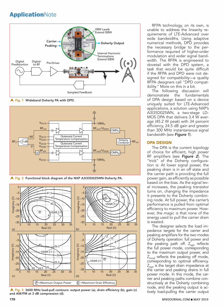
Fig. 2 Functional block diagram of the NXP A3I35D025WN Doherty PA.
OMNc
OMNp
VDS1B
VGS1AVGS2A
VGS1BVGS2B
RFinB
–90˚
0˚
RFin –3 dB
RFinA
VDS1A
VBWB
RFout2/VDS2B
VBWA
RFout1/VDS2A
DohertyCombiner RFout
Quiescent CurrentTemperature Compensation
Quiescent CurrentTemperature Compensation
ϕ
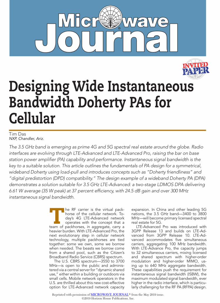
RFPA technology, on its own, is unable to address the linearity re-quirements of LTE-Advanced over wide bandwidths. Using adaptive numerical methods, DPD provides the necessary bridge to the per-formance required of higher-order modulation and wider signal band-width. The RFPA is engineered to dovetail with the DPD system, a task that would be quite difficult if the RFPA and DPD were not de-signed for compatibility—a quality RFPA designers call “DPD compat-ibility.” More on this in a bit.
The following discussion will demonstrate the fundamentals of DPA design based on a device uniquely suited for LTE-Advanced applications, a solution using NXP’s A3I35D025WN, a two-stage LD-MOS DPA that delivers 3.4 W aver-age (45.2 W peak) with 34 percent efficiency, 24.5 dB gain and greater than 300 MHz instantaneous signal bandwidth (see Figure 1).
DPA DESIGNThe DPA is the current topology
of choice for efficient, high power RF amplifiers (see Figure 2). The “trick” of the Doherty configura-tion is: At lower signal power, the peaking drain is in an off state and the carrier path is providing the full power gain, as efficiently as possible based on the bias. As the signal lev-el increases, the peaking transistor turns on, changing the impedance it presents to the Doherty combin-ing node. At full power, the carrier’s performance is pulled from optimal efficiency to maximum power. How-ever, the magic is that none of the energy used to pull the carrier drain is wasted.
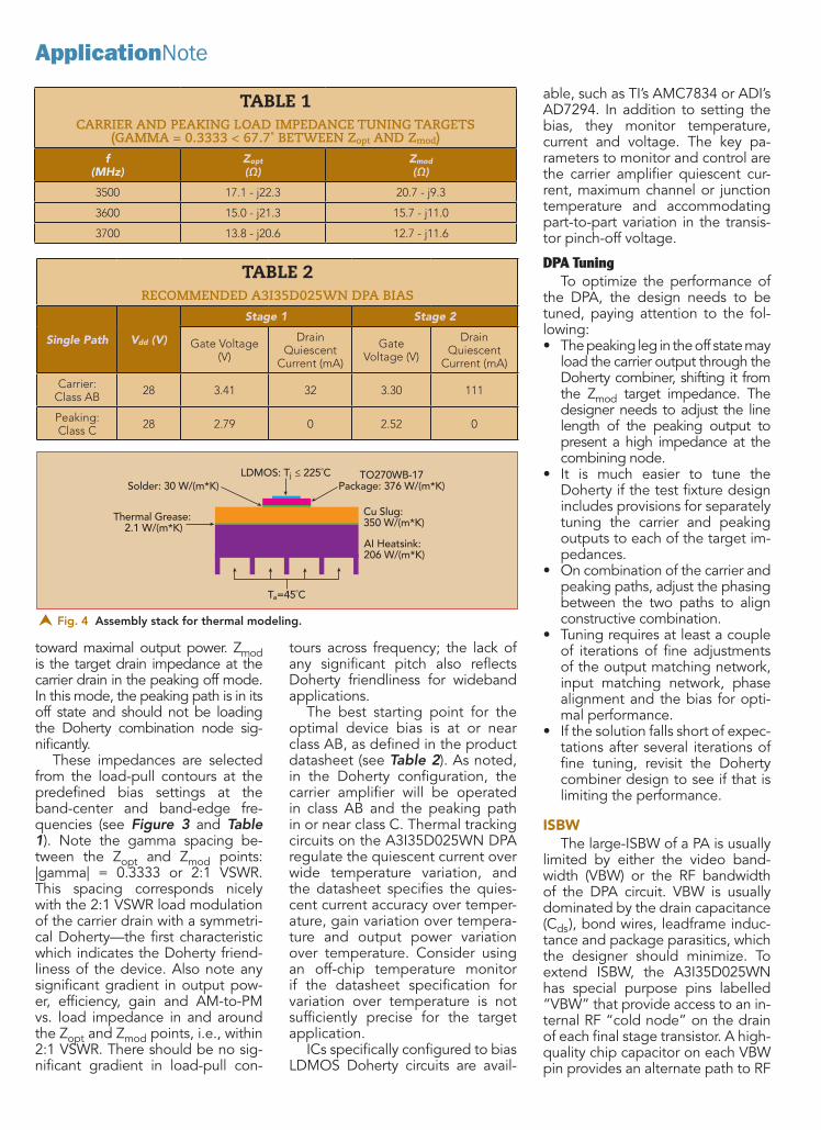
The designer selects the load im-pedance targets for the carrier and peaking amplifiers for the two modes of Doherty operation: full power and the peaking path off. Zopt reflects the full power mode, corresponding to the maximum output power, and Zmod reflects the peaking off mode, corresponding to optimal efficiency. Zopt is the target drain impedance at the carrier and peaking drains in full power mode. In this mode, the car-rier and peaking paths combine con-structively at the Doherty combining node, and the peaking output is ac-tively load-pulling the carrier output Fig. 3 3600 MHz load-pull contours: output power (a), drain efficiency (b), gain (c)
and AM/PM at 3 dB compression (d).
(a) (b)
(c)
0
–5
–10
–15
–20
–25
–30
Imag
inar
y (Ω
)
5 10 15 25Real (Ω)
30 35
41
42
41.5
42.5
43VSWR 2:1
E
P
20
0
–5
–10
–15
–20
–25
–30
Imag
inar
y (Ω
)
5 10 15 25Real (Ω)
30 3520
60
VSWR 2:1
E
P
5856
54
52
0
–5
–10
–15
–20
–25
–30
Imag
inar
y (Ω
)
5 10 15 25Real (Ω)
30 3520
0
–5
–10
–15
–20
–25
–30
Imag
inar
y (Ω
)
5 10 15 25Real (Ω)
30 3520
VSWR 2:1
E
P
–10–8
–6
–4
24
VSWR 2:1
E
P
24.5 25
26
27
25.5
26.5
–12
(d)
EP =Maximum Output Power =Maximum Drain Efciency
ApplicationNote
able, such as TI’s AMC7834 or ADI’s AD7294. In addition to setting the bias, they monitor temperature, current and voltage. The key pa-rameters to monitor and control are the carrier amplifier quiescent cur-rent, maximum channel or junction temperature and accommodating part-to-part variation in the transis-tor pinch-off voltage.
DPA TuningTo optimize the performance of
the DPA, the design needs to be tuned, paying attention to the fol-lowing:• The peaking leg in the off state may
load the carrier output through the Doherty combiner, shifting it from the Zmod target impedance. The designer needs to adjust the line length of the peaking output to present a high impedance at the combining node.
• It is much easier to tune the Doherty if the test fixture design includes provisions for separately tuning the carrier and peaking outputs to each of the target im-pedances.
• On combination of the carrier and peaking paths, adjust the phasing between the two paths to align constructive combination.
• Tuning requires at least a couple of iterations of fine adjustments of the output matching network, input matching network, phase alignment and the bias for opti-mal performance.
• If the solution falls short of expec-tations after several iterations of fine tuning, revisit the Doherty combiner design to see if that is limiting the performance.
ISBWThe large-ISBW of a PA is usually
limited by either the video band-width (VBW) or the RF bandwidth of the DPA circuit. VBW is usually dominated by the drain capacitance (Cds), bond wires, leadframe induc-tance and package parasitics, which the designer should minimize. To extend ISBW, the A3I35D025WN has special purpose pins labelled “VBW” that provide access to an in-ternal RF “cold node” on the drain of each final stage transistor. A high-quality chip capacitor on each VBW pin provides an alternate path to RF
tours across frequency; the lack of any significant pitch also reflects Doherty friendliness for wideband applications.
The best starting point for the optimal device bias is at or near class AB, as defined in the product datasheet (see Table 2). As noted, in the Doherty configuration, the carrier amplifier will be operated in class AB and the peaking path in or near class C. Thermal tracking circuits on the A3I35D025WN DPA regulate the quiescent current over wide temperature variation, and the datasheet specifies the quies-cent current accuracy over temper-ature, gain variation over tempera-ture and output power variation over temperature. Consider using an off-chip temperature monitor if the datasheet specification for variation over temperature is not sufficiently precise for the target application.
ICs specifically configured to bias LDMOS Doherty circuits are avail-
toward maximal output power. Zmod is the target drain impedance at the carrier drain in the peaking off mode. In this mode, the peaking path is in its off state and should not be loading the Doherty combination node sig-nificantly.
These impedances are selected from the load-pull contours at the predefined bias settings at the band-center and band-edge fre-quencies (see Figure 3 and Table 1). Note the gamma spacing be-tween the Zopt and Zmod points: |gamma| = 0.3333 or 2:1 VSWR. This spacing corresponds nicely with the 2:1 VSWR load modulation of the carrier drain with a symmetri-cal Doherty—the first characteristic which indicates the Doherty friend-liness of the device. Also note any significant gradient in output pow-er, efficiency, gain and AM-to-PM vs. load impedance in and around the Zopt and Zmod points, i.e., within 2:1 VSWR. There should be no sig-nificant gradient in load-pull con-
TABLE 1CARRIER AND PEAKING LOAD IMPEDANCE TUNING TARGETS
(GAMMA = 0.3333 < 67.7˚ BETWEEN Zopt AND Zmod)
f (MHz)
Zopt (Ω)
Zmod (Ω)
3500 17.1 - j22.3 20.7 - j9.3
3600 15.0 - j21.3 15.7 - j11.0
3700 13.8 - j20.6 12.7 - j11.6
TABLE 2RECOMMENDED A3I35D025WN DPA BIAS
Single Path Vdd (V)
Stage 1 Stage 2
Gate Voltage (V)
Drain Quiescent
Current (mA)
Gate Voltage (V)
Drain Quiescent
Current (mA)
Carrier: Class AB 28 3.41 32 3.30 111
Peaking: Class C 28 2.79 0 2.52 0
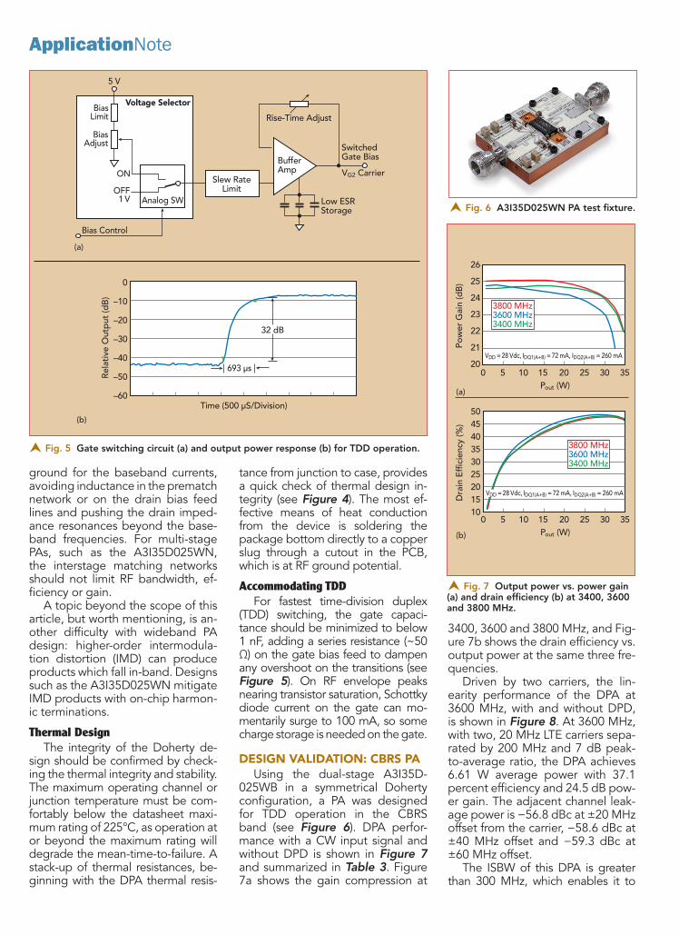
Fig. 4 Assembly stack for thermal modeling.
Solder: 30 W/(m*K)TO270WB-17
Package: 376 W/(m*K)LDMOS: Tj ≤ 225˚C
Thermal Grease: 2.1 W/(m*K)
Cu Slug: 350 W/(m*K)
AI Heatsink: 206 W/(m*K)
Ta=45˚C
ApplicationNote
tance from junction to case, provides a quick check of thermal design in-tegrity (see Figure 4). The most ef-fective means of heat conduction from the device is soldering the package bottom directly to a copper slug through a cutout in the PCB, which is at RF ground potential.
Accommodating TDDFor fastest time-division duplex
(TDD) switching, the gate capaci-tance should be minimized to below 1 nF, adding a series resistance (~50 Ω) on the gate bias feed to dampen any overshoot on the transitions (see Figure 5). On RF envelope peaks nearing transistor saturation, Schottky diode current on the gate can mo-mentarily surge to 100 mA, so some charge storage is needed on the gate.
DESIGN VALIDATION: CBRS PAUsing the dual-stage A3I35D-
025WB in a symmetrical Doherty configuration, a PA was designed for TDD operation in the CBRS band (see Figure 6). DPA perfor-mance with a CW input signal and without DPD is shown in Figure 7 and summarized in Table 3. Figure 7a shows the gain compression at
ground for the baseband currents, avoiding inductance in the prematch network or on the drain bias feed lines and pushing the drain imped-ance resonances beyond the base-band frequencies. For multi-stage PAs, such as the A3I35D025WN, the interstage matching networks should not limit RF bandwidth, ef-ficiency or gain.
A topic beyond the scope of this article, but worth mentioning, is an-other difficulty with wideband PA design: higher-order intermodula-tion distortion (IMD) can produce products which fall in-band. Designs such as the A3I35D025WN mitigate IMD products with on-chip harmon-ic terminations.
Thermal DesignThe integrity of the Doherty de-
sign should be confirmed by check-ing the thermal integrity and stability. The maximum operating channel or junction temperature must be com-fortably below the datasheet maxi-mum rating of 225°C, as operation at or beyond the maximum rating will degrade the mean-time-to-failure. A stack-up of thermal resistances, be-ginning with the DPA thermal resis-
3400, 3600 and 3800 MHz, and Fig-ure 7b shows the drain efficiency vs. output power at the same three fre-quencies.
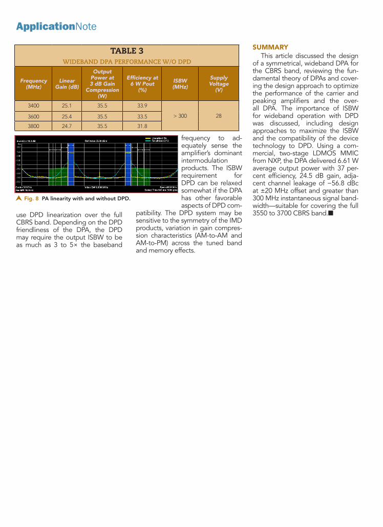
Driven by two carriers, the lin-earity performance of the DPA at 3600 MHz, with and without DPD, is shown in Figure 8. At 3600 MHz, with two, 20 MHz LTE carriers sepa-rated by 200 MHz and 7 dB peak-to-average ratio, the DPA achieves 6.61 W average power with 37.1 percent efficiency and 24.5 dB pow-er gain. The adjacent channel leak-age power is −56.8 dBc at ±20 MHz offset from the carrier, −58.6 dBc at ±40 MHz offset and −59.3 dBc at ±60 MHz offset.
The ISBW of this DPA is greater than 300 MHz, which enables it to
Fig. 5 Gate switching circuit (a) and output power response (b) for TDD operation.
(a)
(b)
0
–10
–20
–30
–40
–50
–60
Rel
ativ
e O
utp
ut (d
B)
Rise-Time Adjust
BufferAmp
SwitchedGate Bias
VG2 Carrier
Analog SW
Bias Control
BiasAdjust
BiasLimit
ON
OFF1 V
Voltage Selector
5 V
Slew RateLimit
Low ESRStorage
Time (500 μS/Division)
32 dB
693 μs
Fig. 6 A3I35D025WN PA test fixture.
Fig. 7 Output power vs. power gain (a) and drain efficiency (b) at 3400, 3600 and 3800 MHz.
frequency to ad-equately sense the amplifier’s dominant intermodulation products. The ISBW requirement for DPD can be relaxed somewhat if the DPA has other favorable aspects of DPD com-
patibility. The DPD system may be sensitive to the symmetry of the IMD products, variation in gain compres-sion characteristics (AM-to-AM and AM-to-PM) across the tuned band and memory effects.
use DPD linearization over the full CBRS band. Depending on the DPD friendliness of the DPA, the DPD may require the output ISBW to be as much as 3 to 5× the baseband
TABLE 3WIDEBAND DPA PERFORMANCE W/O DPD
Frequency (MHz)
Linear Gain (dB)
Output Power at 3 dB Gain
Compression (W)
Efficiency at 6 W Pout
(%)
ISBW (MHz)
Supply Voltage
(V)
3400 25.1 35.5 33.9
> 300 283600 25.4 35.5 33.5
3800 24.7 35.5 31.8
Fig. 8 PA linearity with and without DPD.
SUMMARYThis article discussed the design
of a symmetrical, wideband DPA for the CBRS band, reviewing the fun-damental theory of DPAs and cover-ing the design approach to optimize the performance of the carrier and peaking amplifiers and the over-all DPA. The importance of ISBW for wideband operation with DPD was discussed, including design approaches to maximize the ISBW and the compatibility of the device technology to DPD. Using a com-mercial, two-stage LDMOS MMIC from NXP, the DPA delivered 6.61 W average output power with 37 per-cent efficiency, 24.5 dB gain, adja-cent channel leakage of −56.8 dBc at ±20 MHz offset and greater than 300 MHz instantaneous signal band-width—suitable for covering the full 3550 to 3700 CBRS band.n