Design of a 4-bit 1.4 GSamples/s Low Power Folding ADC for DS-CDMA UWB Transceivers Rajesh Thirugnanam and Dong Sam Ha VTVT (Virginia Tech VLSI for Telecommunications) Lab Department of Electrical and Computer Engineering Virginia Tech, Blacksburg, VA - 24061 Email: {thirugnr,ha}@vt.edu Abstract-In this paper, we present a CMOS low power folding ADC (analog to digital converter) architecture, which takes advantage of the low resolution requirement of DS-CDMA UWB transceivers to reduce the power consumption. The high sampling rate is achieved by adopting current steering folding amplifiers instead of cross coupled differential pair based folding amplifiers. Our ADC adopts both resistive interpolation and multiplication to fold the input signal, thereby, reducing the number of folding amplifiers required. When this technique is applied to higher resolution converters, the power and area savings will be even more significant. A brief analysis on the operation of the folding amplifier and a systematic method for sizing preamplifiers, folding amplifiers and comparators is presented. The ADC has been designed in 0.13 ,um IBM CMOS process. Post layout simulation shows that the spurious free dynamic range (SFDR) of our ADC is greater than 24 dB up to 540 MHz at 1.4 GS/s and consumes about 62 mW of power. The results also indicate that the proposed architecture consumes less power and achieves a higher sampling rate than existing folding ADCs. Index Terms-DS-CDMA, SFDR, UWB, current steering folding amplifier, folding ADC, multiplier I. INTRODUCTION Our DS-CDMA UWB transceiver operates for the low band from 3.1 GHz to 5.15 GHz. After the down conversion followed by a lowpass filter, the data signal occupies a bandwidth of just over 1 GHz. Our system design of the UWB transceiver requires that the ADC operate at the sampling rate of 1.3 GS/s with a 4-bit resolution. Another requirement for our ADC is a high spurious free dynamic range (SFDR) of 24 dB up to 500 MHz and low power dissipation. The low power requirement eliminates the possibility of adopting flash architectures such as the ones in [1]-[3]. A folding ADC architecture is suitable for moderate resolution and low power applications, but its sampling rate without time-interleaving is limited to a few hundred MHz so far. A time-interleaved folding ADC such as the one reported in [4] can achieve a sampling rate beyond one GS/s, but it is excluded from our consideration due to high power dissipation and high circuit complexity. Two types of folding amplifiers, one based on cross coupled differential pair (CCDP) [5] and the other based on current steering (CS) [6], have been proposed for folding ADCs. The number of comparators required for a folding ADC decreases as the folding order increases. With a CCDP folding amplifier, the parasitic capacitance at the amplifier output increases rapidly as the folding order increases, thereby, greatly reducing the achievable sampling rates [7]. In contrast, the output capacitance of a CS folding amplifier, increases much more slowly as the folding order Sang S. Choi Wireless Home Network Research Team Digital Home Research Division Electronics and Telecommunications Research Institute Yueseong-Gu, Deajon,Korea Email: sschoi(&.etri.re.kr increases [6]. However, since the transistors are stacked vertically for a CS folding amplifier, the available headroom decreases with the increase of the folding order, which makes it unsuitable for low voltage applications. So far, all existing folding ADCs employ 3X or 4X single stage folding due to this reason. Our ADC adopts 8X folding based on a CS folding amplifier to increase the sampling rate beyond GS/s. An 8X folding was achieved for our design using two 4X CS folding amplifiers along with an analog multiplier [8]. The remainder of the paper is organized as follows. Section II describes the folding ADC architecture as well as the operation of the current steering folding amplifier. Section III describes the proposed ADC design including a systematic method for optimal transistor sizing and the accompanying digital logic. Section IV presents the simulation results, and section V concludes the paper. II. PRELIMINARIES This section reviews the operation of a typical folding ADC, a CS folding amplifier and an analog amplifier used for our 8X folding amplifier. 2.1 Operation of a typical Folding ADC Fig. 1 shows a block diagram of a conventional 4X folding ADC architecture. The flash ADC produces the two MSBs splitting the search space into four regions. The 4X folding amplifiers split each of the four regions into four subdivisions and the digital encoder generates the corresponding two LSBs. Thus apart from two MSBs which require 3 comparators, the folding part requires 4 comparators. Ref VIN ,VRBI 'A Folding Amplifiers Comparators Fig. 1: Block diagram of a conventional 4-bit folding ADC The folding architecture is a low power alternative to the flash architecture because it reduces the number of comparators required. However, the folding architecture has been limited 536
Transcript
Design of a 4-bit 1.4 GSamples/s Low Power Folding ADC for DS-CDMA UWBTransceivers
Rajesh Thirugnanam and Dong Sam Ha
VTVT (Virginia Tech VLSI for Telecommunications) LabDepartment of Electrical and Computer Engineering
Virginia Tech, Blacksburg, VA - 24061Email: {thirugnr,ha}@vt.edu
Abstract-In this paper, we present a CMOS low power foldingADC (analog to digital converter) architecture, which takesadvantage of the low resolution requirement of DS-CDMA UWBtransceivers to reduce the power consumption. The high samplingrate is achieved by adopting current steering folding amplifiersinstead of cross coupled differential pair based folding amplifiers.Our ADC adopts both resistive interpolation and multiplication tofold the input signal, thereby, reducing the number of foldingamplifiers required. When this technique is applied to higherresolution converters, the power and area savings will be evenmore significant. A brief analysis on the operation of the foldingamplifier and a systematic method for sizing preamplifiers,folding amplifiers and comparators is presented. The ADC hasbeen designed in 0.13 ,um IBM CMOS process. Post layoutsimulation shows that the spurious free dynamic range (SFDR) ofour ADC is greater than 24 dB up to 540 MHz at 1.4 GS/s andconsumes about 62 mW of power. The results also indicate thatthe proposed architecture consumes less power and achieves ahigher sampling rate than existing folding ADCs.
Index Terms-DS-CDMA, SFDR, UWB, current steering foldingamplifier, folding ADC, multiplier
I. INTRODUCTION
Our DS-CDMA UWB transceiver operates for the low bandfrom 3.1 GHz to 5.15 GHz. After the down conversionfollowed by a lowpass filter, the data signal occupies abandwidth ofjust over 1 GHz. Our system design of the UWBtransceiver requires that the ADC operate at the sampling rateof 1.3 GS/s with a 4-bit resolution. Another requirement for ourADC is a high spurious free dynamic range (SFDR) of 24 dBup to 500 MHz and low power dissipation. The low powerrequirement eliminates the possibility of adopting flasharchitectures such as the ones in [1]-[3].A folding ADC architecture is suitable for moderate
resolution and low power applications, but its sampling ratewithout time-interleaving is limited to a few hundred MHz sofar. A time-interleaved folding ADC such as the one reported in[4] can achieve a sampling rate beyond one GS/s, but it isexcluded from our consideration due to high power dissipationand high circuit complexity. Two types of folding amplifiers,one based on cross coupled differential pair (CCDP) [5] and theother based on current steering (CS) [6], have been proposedfor folding ADCs. The number of comparators required for afolding ADC decreases as the folding order increases. With aCCDP folding amplifier, the parasitic capacitance at theamplifier output increases rapidly as the folding orderincreases, thereby, greatly reducing the achievable samplingrates [7]. In contrast, the output capacitance of a CS foldingamplifier, increases much more slowly as the folding order
Sang S. Choi
Wireless Home Network Research TeamDigital Home Research Division
Electronics and Telecommunications Research InstituteYueseong-Gu, Deajon,Korea
Email: sschoi(&.etri.re.kr
increases [6]. However, since the transistors are stackedvertically for a CS folding amplifier, the available headroomdecreases with the increase ofthe folding order, which makes itunsuitable for low voltage applications. So far, all existingfolding ADCs employ 3X or 4X single stage folding due to thisreason. Our ADC adopts 8X folding based on a CS foldingamplifier to increase the sampling rate beyond GS/s. An 8Xfolding was achieved for our design using two 4X CS foldingamplifiers along with an analog multiplier [8].
The remainder of the paper is organized as follows. SectionII describes the folding ADC architecture as well as theoperation of the current steering folding amplifier. Section IIIdescribes the proposed ADC design including a systematicmethod for optimal transistor sizing and the accompanyingdigital logic. Section IV presents the simulation results, andsection V concludes the paper.
II. PRELIMINARIES
This section reviews the operation of a typical folding ADC,a CS folding amplifier and an analog amplifier used for our 8Xfolding amplifier.
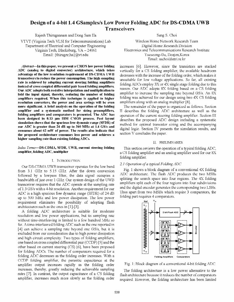
2.1 Operation ofa typical FoldingADCFig. 1 shows a block diagram of a conventional 4X folding
ADC architecture. The flash ADC produces the two MSBssplitting the search space into four regions. The 4X foldingamplifiers split each of the four regions into four subdivisionsand the digital encoder generates the corresponding two LSBs.Thus apart from two MSBs which require 3 comparators, thefolding part requires 4 comparators.
Ref VIN
,VRBI 'AFolding Amplifiers Comparators
Fig. 1: Block diagram of a conventional 4-bit folding ADC
The folding architecture is a low power alternative to theflash architecture because it reduces the number of comparatorsrequired. However, the folding architecture has been limited
536
mostly for low resolution ADCs such as 4- to 8-bit ADCs dueto technical difficulties in implementing high order foldingamplifiers with high speed and/or large input bandwidth. Thefolding operation effectively increases the output frequency ofa folding amplifier as given in the following relationship [5].The instantaneous output frequencyf11, is
lout ;-IFFF*('1f)where FF is the folding factor andfn, is the input frequency.Hence, the output frequency is proportional to the foldingfactor, thereby, restricting the input bandwidth ofthe converter.
2.2 Current Steering Folding AmplifierA key component for folding ADCs is folding amplifiers.
CCDP folding amplifiers have been widely used [4], [5], [10].A CCDP folding amplifier achieves the folding characteristicby alternately summing the positive and negative outputs ofconsecutive differential pairs. A CCDP folding amplifierrequires as many well-matched differential pairs as the foldingorder. Further, a CCDP folding amplifier restricts thedifference of two consecutive reference voltages IlVr as givenbelow [5].
AVr > 2. 2 1tail (2)
where Itail is the tail current of each differential pair, ,u is thechannel mobility, and cox is the gate oxide capacitance per unitarea. This restriction is due to the fact that the zero crossingshave to be sufficiently far apart to ensure that there is nooverlap in the folding characteristics.Guo et al. proposed a CS folding amplifier to address the
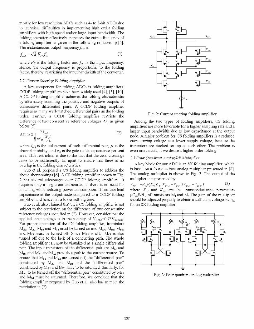
above shortcomings [6]. A CS folding amplifier shown in Fig.2 has several advantages over CCDP folding amplifiers. Itrequires only a single current source, so there is no need formatching while reducing power consumption. It has less loadcapacitance at the output node compared to a CCDP foldingamplifier and hence has a lower settling time.Guo et al. also claimed that their CS folding amplifier is not
subject to the restriction on the difference of two consecutivereference voltages specified in (2). However, consider that theapplied input voltage is in the vicinity of VREF3=0.75Vin(max).For proper operation of the 4X folding amplifier, transistorsMAI, MA2> MB4 and Mc4 must be turned on and MA4, MB1, MB2>and MC2 must be turned off. Since MB2 iS off, Mc3 is alsoturned off due to the lack of a conducting path. The wholefolding amplifier can now be visualized as a single differentialpair. The input transistors of the differential pair are MA3 andMB3 and MAI and MA2 provide a path to the current source. Toensure that MB1 and MB2 are turned off, the "differential pair"constituted by MAI and MB1 and the "differential pair"constituted by MA2 and MB2 have to be saturated. Similarly, forMA4 to be turned off the "differential pair" constituted by MA4and MB4 must be saturated. Therefore, we conclude that thefolding amplifier proposed by Guo et al. also has to meet therestriction in (2).
Fig. 2: Current steering folding amplifier
Among the two types of folding amplifiers, CS foldingamplifiers are more favorable for a higher sampling rate and alarger input bandwidth due to low capacitance at the outputnode. A major problem for CS folding amplifiers is a reducedoutput swing voltage at a lower supply voltage, because thetransistors are stacked on top of each other. The problem iseven more acute, ifwe desire a higher order folding.
2.3 Four Quadrant Analog/RF MultiplierA key block for our ADC is an 8X folding amplifier, which
is based on a four quadrant analog multiplier presented in [8].The analog multiplier is shown in Fig. 3. The output of themultiplier is represented byVout RO1IRRKnlKn4(VINI+ -VINI-)(VIN2+ -VIN2-) (3)
where Knl and Kn4 are the transconductance parametersptCo,W/L, of transistors M1 and M4.The gain of the multipliershould be adjusted properly to obtain a sufficient voltage swingfor an 8X folding amplifier.
Fig. 3: Four quadrant analog multiplier
537
III. PROPOSED ADC DESIGN
This section describes the overall architecture of theproposed folding ADC, a technique to design an 8X CS foldingamplifier, and a systematic transistor sizing scheme for threemajor building blocks of our folding ADC.
3.1 Overall ArchitectureThe block diagram of our folding ADC is shown in Fig. 4. A
flash ADC generates the 2 MSBs, and the remaining two LSBsare generated from folding amplifiers. The input and thereference voltages are differential to reduce the common modenoise.
The 2-bit flash ADC consists ofthree preamplifiers followedby sample-and-hold (S/H) circuits. Each S/H has a dummyswitch, which is always closed, to absorb charge injectioneffects [11 ]. A S/H is followed by a resistive averaging block toreduce random mismatches and offset errors [9]. The resistiveaveraging block distributes the mismatch currents due toprocess variations and smoothes out large variations.
The folding part has an array of eight preamplifiers followedby S/Hs. The outputs of the S/Hs are averaged by resistiveaveraging and then applied to two CS 4X folding amplifiers.The outputs of the 4X folding amplifiers are interpolated usingtwo resistors, and the following comparator decides the thirdbit. The final bit, the LSB, is decided by an 8X foldingamplifier, which is implemented through multiplication of thetwo 4X folding amplifier outputs.
The zero-crossing points ofthe folding amplifiers are criticalfor any folding ADCs. The zero-crossing points for the top 4X
folding amplifier are vl"j6P) (1, 5, 9, 13), and that for the
bottom amplifier are 16P (3, 7, 11, 15). When the two
amplifier outputs are interpolated, the zero-crossing points
become i16 D (2, 6, 10, 14). So the comparator output can beused to determine the third bit of our ADC.
As discussed earlier, a CS folding amplifier stacks transistorsvertically. Hence, a direct extension of a 4X folding shown inFig. 2 will not work for an 8X folding amplifier operating at alow supply voltage. Instead, we implement an 8X folding
amplifier by multiplying the outputs of the two 4X foldingamplifiers using a four quadrant analog multiplier shown inFig. 3. The zero-crossing points of the 8X folding amplifier isthe union of zero-crossing points of the two 4X folding
amplifiers, and they are 16 (1, 3, 5, 7, 9, 11, 13, 15). Theodd numbered zero crossing-points are used to determine theLSB of the ADC.
Fig. 5 shows the SPICE simulation of the two foldingamplifiers, the resistive interpolation, and the multiplier outputand the waveforms verify the zero-crossing points discussedabove.
/@nn a Folder 4- Folder2
Interpolation
9.09 n(p-p) X / 1
Multiplier
.4m
Wdin
Fig. 5: Transfer characteristics of4X and 8X foldingamplifiers
Compared with the conventional ADC shown in Fig. 1, themain advantages of the proposed folding ADC architecture arelow hardware complexity and high speed. The proposed ADCsaves two 4X folding amplifiers and two comparators at thecost of one additional analog multiplier. So the proposedarchitecture reduces the overall circuit complexity to result inlow power dissipation. In other words, use of only two 4Xfolding amplifiers to decide the two LSBs is unique for theproposed design and effective for reduction of hardwarecomplexity and power dissipation. This technique may beapplicable for higher resolution ADCs as well.
3.2 Analog Building BlocksLike any analog circuit design, transistor sizing is a key
design issue for the proposed folding ADC. Transistor sizinghas been discussed in detail for flash ADCs, but little work hasbeen done for folding ADCs [1], [2], [14]. In this section, wedescribe our approach to determine transistor sizes for threemajor building blocks: preamplifiers, folding amplifiers, andcomparators. We decided initial transistor sizes based on anapproximate input/output relationship of each block and thenfine tuned the sizes through simulation.
The target Integral nonlinearity (INL) of our ADC is set to0, 1Vi pp0.1 LSB or n(p So an input voltage which differs from
16~~~~~~~~~~~~~~~~~~~~~any particular reference voltage level by at least i16-'should be resolved into the corresponding digital output codewithin one period of the sampling clock.
538
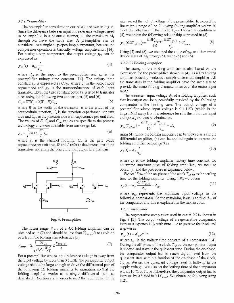
3.2.1 PreamplifierThe preamplifier considered in our ADC is shown in Fig. 6.
Since the difference between input and reference voltages needto be amplified in a balanced manner, all the transistors M1through M4 have the same size. A preamplifier can beconsidered as a single step/open loop comparator, because thecomparison operation is basically voltage amplification [14].For a single step comparator, the output voltage Ypa can beexpressed as
Ypa(t) =dpa t (4)zpa
where dpa is the input to the preamplifier and Tpa is thepreamplifier unitary time constant [14]. The unitary timeconstant Tpa is expressed as C0gm, where C0 is the output nodecapacitance and gm is the transconductance of each inputtransistor. Thus, the time constant could be related to transistorsizes using the following two expressions, (5) and (6)CO = WECJ + 2(W + E)Cj1, (5)where W is the width of the transistor, E is the width of thesource/drain junction, Ci is the junction capacitance per unitarea and Cj,> is the junction side wall capacitance per unit area.The values of E, Cj and Cj,> values are specific to the processtechnology and were available from our design kit.
gn = 2y,C0x Ltail (6)
where qu is the channel mobility, Cox is the gate oxidecapacitance per unit area, Wand L refer to the dimensions ofthetransistors and Itail is the bias current of the differential pair.
RL RL
VOUT VOUT+
VIN+-] M2 0VREF V 3 4 -0 VIN
4, 'TAIL 4 'TAIL
Fig. 6: Preamplifier
The linear range Vlinear of a 4X folding amplifier can beobtained as in (7) and should be less than Vin( p/14 to avoid anoverlap in the folding characteristics [5].
2linear|22tail < Vin(p-p) (7)r nCox W/L 4
For a preamplifier whose input reference voltage is away fromthe input voltage by more than 0.5 LSB, the preamplifier outputvoltage should be large enough to drive the differential pair ofthe following CS folding amplifier to saturation, so that thefolding amplifier works as a single differential pair, asdescribed in Section 2.2. In order to meet the required sampling
rate, we set the output voltage of the preamplifier to exceed thelinear input range of the following folding amplifier within 8000 of the off-phase of the clock, Tofflk. Using the condition in(4), we obtain the following relationship expressed in (8)
yp (0 8Toffc 0.5VO(PTP) D 2Vlk e (8)Ypa(8Tofcl) = n(p offcl > Vlna'U l pa
Using (7) and (8), we obtained the value of Tpa, and then initialdevice sizes of M1 through M4 using (5) and (6).
3.2.2 CS Folding AmplifierThe sizing of the folding amplifier is also based on the
expression for the preamplifier shown in (4), as a CS foldingamplifier basically works as a simple differential amplifier. Allthe transistors in the folding amplifier have the same size toprovide the same folding characteristics over the entire inputrange.
The minimum input voltage dfa of a folding amplifier suchthat its output can be successfully resolved by the followingcomparator is the limiting case. The output voltage of apreamplifier whose input voltage is 0.1 LSB (which is thetarget INL) away from its reference level is the minimum inputvoltage dfa and can be obtained as
"in(pp Toff,clk =df9Ypa (Toff,clk 1 a fa (9)
using (4). Since the folding amplifier can be viewed as a simpledifferential amplifier, (4) can be applied again to express thefolding amplifier output yfa(t) as
(10)yf (t) = dfa
Tfa
where Ifa is the folding amplifier unitary time constant. Todetermine transistor sizes of folding amplifiers, we need toobtain Ifa, and the procedure is explained below.We set 15 00 ofthe on-phase ofthe clock Tn, elk as the settling
time for the folding amplifier. Using (10), we obtain
Y() d 0.O15Tnlc dr (1=1)Tfa
where drgc represents the minimum input voltage to thefollowing comparator. So the remaining issue is to find drgc ofthe comparator and this is explained in the next section.
3.2.3 ComparatorThe regenerative comparator used in our ADC is shown in
Fig. 7 [2]. The output voltage of a regenerative comparatorincreases exponentially with time, due to positive feedback andis given as
Yrgc(t) drgce' g (12)
where Trgc is the unitary time constant of a comparator [14].During the off-phase ofthe clock, Toff lk, the comparator outputis shorted and stays in the quiescent state. During the on-phase,the comparator output has to reach digital level from thequiescent state within a fraction of the on-phase of the clock,Ton, clk. We set the quiescent voltage level at halfway to thesupply voltage. We also set the settling time of the comparatorwithin 10 00 of Ton,clk. Therefore, the comparator output has toincrease by 0.5 Vdd in 0.1 Ton, clk. We obtain the following using(12).
539
0.5Vdd = drgce°lToTrg (13)
We picked several candidate unitary time constants rIrgc andthen determined drgc using (13). The unitary time constants canbe related to transistor sizes as follows
Trgc= COK1 g
gm,p gm,nwhere gm,p and gmn, are the transconductance of PMOS andNMOS transistors, respectively. The output node capacitanceC0 is expressed as
Co = CDBP + CDBn + CGSP +CGSn (15)The expression for drain-bulk capacitance is given in (5), andthe gate-source capacitance is approximately expressed as
2CGS =WLCJ'
Fig. 7: Regenerative comparator
Although the above guidelines are based on approximateanalyses, they proved to be an effective tool for determininginitial transistor sizes and to estimate the maximum achievablesampling rate.
3.3 Digital EncoderThe block diagram of the digital encoder is shown in Fig. 8.
True single phase clock (TSPC) latches capture the comparatoroutputs, and sense amplifier based flip-flops synchronize theinputs to the encoding logic [12], [13]. The encoding logicconverts the gray-coded comparator outputs to the binary code,and another set of sense amplifier based flip-flops synchronizethe encoded outputs.
In order to test our standalone ADC, we have added adecimator, which decimates the outputs by 16. An externalcontrol input selects between decimated or undecimated data atthe outputs.
Clock
Fig. 8: Block diagram of the digital encoder
IV. POST LAYOUT SIMULATION RESULTS
The proposed folding ADC was laid out in 0.13 pm IBMCMOS technology. The layout of the core part is shown in Fig.9. Guard rings are used around the digital circuitry to minimizecross-talk between analog and digital sections. The ADCoccupied an active area of 0.05 mm2 and consumed 62 mW atthe sampling rate of 1.4 GS/s with the supply voltage of 1.5 V.
Fig. 9: Layout of the core part of the ADC
The design kit enabled use ofMonte Carlo analysis as well ascorner simulations. Therefore, process variations andgeometric mismatches could be included in our simulationwithout going through a behavior model of the ADC. Themaximum INL and DNL were determined with the cornerparameters set to the maximum 3-sigma variation.
Fig. 10 shows INL (integral nonlinearity) and DNL(differential nonlinearity) for the entire range of the outputcode. The results indicate that the peak INL is less than 0.2 LSBand the peak DNL is less than 0.3 LSB. The performance istypical for a low resolution ADC and sufficient for ourapplication. Digital calibration schemes can be used to improvethe static performance at the cost of increased circuitcomplexity and power consumption.
1
0.5 - t t t -
C')~- 0-jz
-0 .5-- -t-
-1
0.5
.0zo -0.5_
-1-
2 4 6 Co8de 10 12 14
2 4 6 8 10 12Code
Fig. 10: INL and DNL performance
14
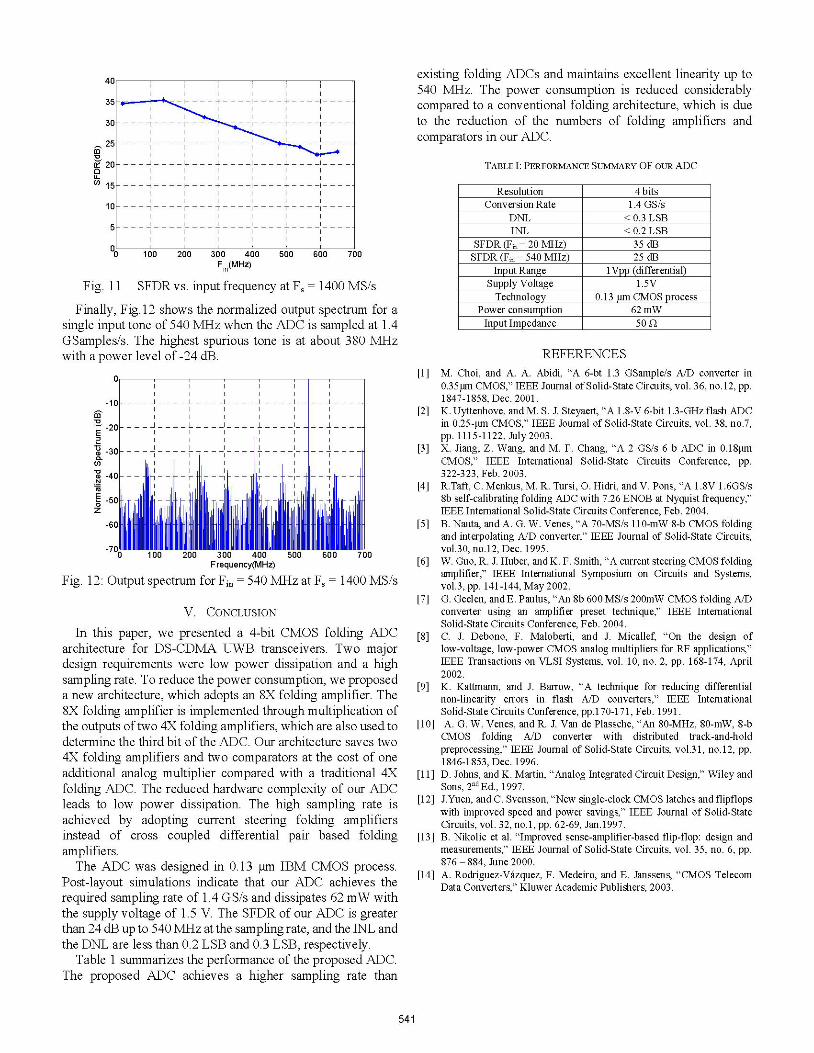
The next simulation was to estimate the variation of SFDRwith an input frequency at the sampling rate of 1.4GSamples/s.The simulation results given in Fig. 11 indicate that the SFDRremains above 24 dB for up to 540 MHz.
540
40
35
30
_ 25mOz 20U-
10-
&0) 100 200 300 400Fin(MHz)
500 600 700
Fig. 11 SFDR vs. input frequency at F, = 1400 MS/s
Finally, Fig. 12 shows the normalized output spectrum for asingle input tone of 540 MHz when the ADC is sampled at 1.4GSamples/s. The highest spurious tone is at about 380 MHzwith a power level of -24 dB.
0
-10 _ L _a
E -20
t -30(DCL)_D -40
E-50
-6(
-74
Frequency(MHz)
Fig. 12: Output spectrum for Fin = 540 MHz at F,
700
1400 MS/s
V. CONCLUSION
In this paper, we presented a 4-bit CMOS folding ADCarchitecture for DS-CDMA UWB transceivers. Two majordesign requirements were low power dissipation and a highsampling rate. To reduce the power consumption, we proposeda new architecture, which adopts an 8X folding amplifier. The8X folding amplifier is implemented through multiplication ofthe outputs oftwo 4X folding amplifiers, which are also used todetermine the third bit of the ADC. Our architecture saves two4X folding amplifiers and two comparators at the cost of oneadditional analog multiplier compared with a traditional 4Xfolding ADC. The reduced hardware complexity of our ADCleads to low power dissipation. The high sampling rate isachieved by adopting current steering folding amplifiersinstead of cross coupled differential pair based foldingamplifiers.
The ADC was designed in 0.13 pm IBM CMOS process.Post-layout simulations indicate that our ADC achieves therequired sampling rate of 1.4 GS/s and dissipates 62 mW withthe supply voltage of 1.5 V. The SFDR of our ADC is greaterthan 24 dB up to 540 MHz at the sampling rate, and the INL andthe DNL are less than 0.2 LSB and 0.3 LSB, respectively.
Table 1 summarizes the performance of the proposed ADC.The proposed ADC achieves a higher sampling rate than
existing folding ADCs and maintains excellent linearity up to540 MHz. The power consumption is reduced considerablycompared to a conventional folding architecture, which is dueto the reduction of the numbers of folding amplifiers andcomparators in our ADC.
[2] K. Uyttenhove, and M. S. J. Steyaert, "A 1.8-V 6-bit 1.3-GHz flash ADCin 0.25-gm CMOS," IEEE Journal of Solid-State Circuits, vol. 38, no.7,pp. 1115-1122, July 2003.
[3] X. Jiang, Z. Wang, and M. F. Chang, "A 2 GS/s 6 b ADC in 0.18gmCMOS," IEEE International Solid-State Circuits Conference, pp.322-323, Feb. 2003.
[4] R.Taft, C. Menkus, M. R. Tursi, 0. Hidri, and V. Pons, "A 1.8V 1.6GS/s8b self-calibrating folding ADC with 7.26 ENOB at Nyquist frequency,"IEEE International Solid-State Circuits Conference, Feb. 2004.
[5] B. Nauta, and A. G. W. Venes, "A 70-MS/s 1 10-mW 8-b CMOS foldingand interpolating A/D converter," IEEE Journal of Solid-State Circuits,vol.30, no.12, Dec. 1995.
[6] W. Guo, R. J. Huber, and K. F. Smith, "A current steering CMOS foldingamplifier," IEEE International Symposium on Circuits and Systems,vol.3, pp. 141-144, May 2002.
[7] G. Geelen, and E. Paulus, "An 8b 600 MS/s 200mW CMOS folding A/Dconverter using an amplifier preset technique," IEEE InternationalSolid-State Circuits Conference, Feb. 2004.
[8] C. J. Debono, F. Maloberti, and J. Micallef, "On the design oflow-voltage, low-power CMOS analog multipliers for RF applications,"IEEE Transactions on VLSI Systems, vol. 10, no. 2, pp. 168-174, April2002.
[9] K. Kattmann, and J. Barrow, "A technique for reducing differentialnon-linearity errors in flash A/D converters," IEEE InternationalSolid-State Circuits Conference, pp.170-171, Feb. 1991.
[10] A. G. W. Venes, and R. J. Van de Plassche, "An 80-MHz, 80-mW, 8-bCMOS folding A/D converter with distributed track-and-holdpreprocessing," IEEE Journal of Solid-State Circuits, vol.31, no.12, pp.1846-1853, Dec. 1996.
[11] D. Johns, and K. Martin, "Analog Integrated Circuit Design," Wiley andSons, 2nd Ed., 1997.
[12] J.Yuen, and C. Svensson, "New single-clock CMOS latches and flipflopswith improved speed and power savings," IEEE Journal of Solid-StateCircuits, vol. 32, no.1, pp. 62-69, Jan.1997.
[13] B. Nikolic et al. "Improved sense-amplifier-based flip-flop: design andmeasurements," IEEE Journal of Solid-State Circuits, vol. 35, no. 6, pp.876- 884, June 2000.
[14] A. Rodriguez-Vazquez, F. Medeiro, and E. Janssens, "CMOS TelecomData Converters," Kluwer Academic Publishers, 2003.