Brigham Young University Brigham Young University BYU ScholarsArchive BYU ScholarsArchive Theses and Dissertations 2011-12-13 Detail Extraction from Electron Backscatter Diffraction Patterns Detail Extraction from Electron Backscatter Diffraction Patterns John A. Basinger Brigham Young University - Provo Follow this and additional works at: https://scholarsarchive.byu.edu/etd Part of the Mechanical Engineering Commons BYU ScholarsArchive Citation BYU ScholarsArchive Citation Basinger, John A., "Detail Extraction from Electron Backscatter Diffraction Patterns" (2011). Theses and Dissertations. 2689. https://scholarsarchive.byu.edu/etd/2689 This Dissertation is brought to you for free and open access by BYU ScholarsArchive. It has been accepted for inclusion in Theses and Dissertations by an authorized administrator of BYU ScholarsArchive. For more information, please contact [email protected], [email protected].
Transcript
Brigham Young University Brigham Young University
BYU ScholarsArchive BYU ScholarsArchive
Theses and Dissertations
2011-12-13
Detail Extraction from Electron Backscatter Diffraction Patterns Detail Extraction from Electron Backscatter Diffraction Patterns
John A. Basinger Brigham Young University - Provo
Follow this and additional works at: https://scholarsarchive.byu.edu/etd
Part of the Mechanical Engineering Commons
BYU ScholarsArchive Citation BYU ScholarsArchive Citation Basinger, John A., "Detail Extraction from Electron Backscatter Diffraction Patterns" (2011). Theses and Dissertations. 2689. https://scholarsarchive.byu.edu/etd/2689
This Dissertation is brought to you for free and open access by BYU ScholarsArchive. It has been accepted for inclusion in Theses and Dissertations by an authorized administrator of BYU ScholarsArchive. For more information, please contact [email protected], [email protected].
Detail Extraction from Electron Backscatter Diffraction Patterns
Jay Basinger
Department of Mechanical Engineering Doctor of Philosophy
Cross-correlation based analysis of electron backscatter diffraction (EBSD) patterns and
the use of simulated reference patterns has opened up entirely new avenues of insight into local lattice properties within EBSD scans. The benefits of accessing new levels of orientation resolution and multiple types of previously inaccessible data measures are accompanied with new challenges in characterizing microscope geometry and other error previously ignored in EBSD systems. The foremost of these challenges, when using simulated patterns in high resolution EBSD (HR-EBSD), is the determination of pattern center (the location on the sample from which the EBSD pattern originated) with sufficient accuracy to avoid the introduction of phantom lattice rotations and elastic strain into these highly sensitive measures.
This dissertation demonstrates how to greatly improve pattern center determination. It
also presents a method for the extraction of grain boundary plane information from single two-dimensional surface scans. These are accomplished through the use of previously un-accessed detail within EBSD images, coupled with physical models of the backscattering phenomena. A software algorithm is detailed and applied for the determination of pattern center with an accuracy of ~0.03% of the phosphor screen width, or ~10µm. This resolution makes it possible to apply a simulated pattern method (developed at BYU) in HR-EBSD, with several important benefits over the original HR-EBSD approach developed by Angus Wilkinson.
Experimental work is done on epitaxially-grown silicon and germanium in order to gauge
the precision of HR-EBSD with simulated reference patterns using the new pattern center calibration approach. It is found that strain resolution with a calibrated pattern center and simulated reference patterns can be as low as 7x10⁻⁴. Finally, Monte Carlo-based models of the electron interaction volume are used in conjunction with pattern-mixing-strength curves of line scans crossing grain boundaries in order to recover 3D grain boundary plane information. Validation of the approach is done using 3D serial scan data and coherent twin boundaries in tantalum and copper. The proposed method for recovery of grain boundary plane orientation exhibits an average error of 3 degrees. Keywords: EBSD, pattern center, cross-correlation, grain boundary orientation, Monte Carlo, electron interaction volume
ACKNOWLEDGMENTS
I am grateful to my graduate committee members: Dr. David Fullwood, Dr. Brent
Adams, Dr. Denise Halverson, Dr. Eric Homer, and Dr. Tracy Nelson, for their help with and
review of this work.
Thank you to the Army Research Office (WF911NF-08-1-0350) and Dr. David Stepp,
Program Director, for funding this research.
Thanks is also due to Josh Kacher, who passed on much of his deep and mysterious
knowledge of cross-correlation based EBSD.
Josh Kacher, Caroline Sorensen, Matt Nowell, and Aimo Winkelmann are gratefully
acknowledged for their contributions to this dissertation.
I was also stuck in the basement of CB 165 for way too long with: Stuart Rogers, Calvin
(CJ) Gardner, Ribeka, Takahashi, Oliver Johnson, Mark Esty, Dan Seegmiller, Sadegh Ahmadi,
Samikshya Subedi, Travis Rampton, Jon Scott, Thomas Hardin, Ali Khosravani, Matthew
Converse, Timothy Ruggles, and several other Lab 165-ers. Great times. Thank you.
Dr. David Fullwood and Dr. Brent Adams deserve copious thanks for the difference they
have made in my life. It has been an honor to work with and learn from them. I also greatly
enjoyed the dissertation topic with the challenge and learning it presented.
The biggest thanks of all go to my wife, Elizabeth (though she will likely never read this).
She has been patient and encouraging in my returning to school, and supportive despite all of the
sacrifices it entailed.
v
TABLE OF CONTENTS
LIST OF TABLES ...................................................................................................................... vii
LIST OF FIGURES ................................................................................................................... viii
Appendix A .................................................................................................................................. 75
vii
LIST OF TABLES
Table 2-1: Pattern Center Optimization Results. X*,Y*, and Z* are reported in percent
of the phosphor screen. ..............................................................................................29
Table 3-1:Dislocation density for at varied PC component error for HR-EBSD with simulated patterns. The tabulated PC errors examined here are very large even when compared with standard EBSD PC calibration method resolution (~0.002). Also displayed are the minimum and maximum errors in dislocation density measurement. The dislocation density when all three components are changed by + or – 0.03 is also reported. PC error is reported as a fraction of the phosphor screen width. ..............................................................................................48
Table 4-1: The predicted φ angle, from the convolution curve comparison and the error between φ's is given. All units are given in degrees. ........................................64
viii
LIST OF FIGURES
Figure 2-1: 2D Schematic of microscope geometry of pattern center for EBSD. ................ 11
Figure 2-2: Phosphor screen to sphere transformation geometry as described in eq. 2. Two different reference frames exist in the definition of this transformation. The X*,Y*,x, and y variables all reside in the plane of the phosphor screen. Z*, γ, xS, yS, and zS are expressed in a global reference frame. ...................................... 13
Figure 2-3: A germanium EBSD pattern projected onto a sphere centered at the PC. The kinematically simulated bands (the grey lines enclosing the bright Kikuchi bands) have been widened by a factor of two from their Bragg angles to ensure that the EBSD bands are fully enclosed. Spherical reference frames in EBSD have been introduced and described by Day (Day, 2008). ....................................... 13
Figure 2-4: Band-realignment and band-profile comparison steps, applied to each Kikuchi band individually. Based on shifts between top and bottom intensity profiles, and distance from the center, a right spherical triangle is used to calculate the angle by which to rotate the simulated bands. Intensity profiles are depicted in the top and bottom quarters of the simulated band (represented by parallel gray lines) and represent the integrated intensities between simulated band edges in the top and bottom halves of the band. .............................. 15
Figure 2-5: Schematic of edges of non-parallel band (in gray) laid over parallel lines (solid black). This represents a band mapped with incorrect PC. ............................. 16
Figure 2-6: Germanium EBSD image projected into the spherical frame. Only non-intersecting regions within widened simulated bands are displayed / considered. ................................................................................................................ 20
Figure 2-7: Simple Bragg's Law based simulated germanium EBSD pattern before (left) and after filtering (right)................................................................................... 23
Figure 2-8: 801 x 801 pixel dynamically simulated Fe-α at 20 keV, courtesy of Winkelmann. X*, Y*, Z* = (50.00%, 50.00%, 49.97%) . ........................................ 24
Figure 2-9: PC component search spaces, demonstrating distinct minima at the correct PC in X*, Y*, and Z* for the dynamically simulated EBSD pattern from Figure 2-8. Points on the graph are spaced 0.02% of the phosphor width apart along the PC Error axis. ............................................................................................ 26
Figure 2-10: Positions of scan points for the single-crystal germanium sample, in PC space, as found by pattern center optimization. Shown in units of fraction of the image/phosphor screen : X*,Y*, and Z*. Measures of distance between points (in microns) are also shown for comparison with the 10 µm square (as
ix
measured by the microscope beam position). PC components are given in terms of fraction of the phosphor width. ....................................................................27
Figure 2-11: Inverse pole figure orientation map of three partial Nickel grains. Grains A, B, and C include accompanying representative EBSD images used for the PC optimization. ........................................................................................................29
Figure 2-12: Phantom strains introduced due to PC error in Z*. Calculated using Wilkinson's method and comparing kinematically simulated patterns with incorrect PC to a strain-free reference simulated pattern. The labeled point indicates a data point near the 7 x 10⁻⁴ strain resolution limit on the y axis for the e11 strain component. PC error is given in terms of fraction of the phosphor screen. ........................................................................................................................32
Figure 3-1: Deformation geometry and projection of shifts onto the phosphor screen. ........36
Figure 3-2: L-grid setup for dislocation density measurement using simulated patterns and a varied PC assumption. ......................................................................................42
Figure 3-3: Average of the absolute value of all strain components for Si and Ge HR-EBSD scans using simulated reference patterns with and without a careful pattern center calibration............................................................................................43
Figure 3-4: Misorientation maps (in degrees) from the average orientation of the PC-calibrated HR-EBSD scan (simulated reference patterns used in all HR-EBSD runs). A) Ge HR-EBSD scan with PC calibration. B) Ge HR-EBSD scan without PC calibration. C) Ge OIM scan. D) Si HR-EBSD with PC calibration. E) Si HR-EBSD without PC calibration. F) Si OIM scan. ........................................44
Figure 3-5: Results obtained in OIMTM software for orientation spread from average and kernel average misorientation plus two times the standard deviation (KAM+2σ) for OIM-only scans, as well as HR-EBSD scans with calibrated and uncalibrated PC for simulated and real reference patterns. All data within the HR-EBSD label used simulated patterns unless "Real Reference" is specified. ....................................................................................................................45
Figure 3-6: Misorientation error vs PC error for Si and Ge HR-EBSD scans as well as theoretical component-wise rotation tensor error vs PC error. ..................................47
Figure 4-1: Reference coordinate frame and electron interaction volume (shown as a red triangle at the point where the electron beam intersects the surface). .................53
Figure 4-2: Grain boundary normal angles, φ and θ. .............................................................53
Figure 4-3: Tantalum interaction volume, shown in the X-Y, and Y-Z planes, indicating the locations of the last significant backscattered electron collisions. Units are in nanometers. The positive z direction in the sample reference frame points into the material...............................................................................................54
x
Figure 4-4: Interaction volume divided by a grain boundary plane. ..................................... 56
Figure 4-5: Fraction of interaction volume on one side of the simulated grain boundary at varied locations along the y-axis ........................................................................... 56
Figure 4-6: Mixed EBSD pattern (middle) with contributing patterns on either side. ......... 57
Figure 4-7: Indexed mixed EBSD image in OIM DC Software. .......................................... 60
Figure 4-8: Simulated image of prominent orientation. ........................................................ 61
Figure 4-9: Indexing of Mixed EBSD image with bands simulated from the stronger orientation removed. ................................................................................................. 61
Figure 4-10: Copper data from FIB serial scans. Grain boundary plane normal angles in phi and theta for scan (layer) four are determined to be θ = 46° and φ = 63°, based on 500 nm spacing between layers. These experimentally determined angles are used for validation. ................................................................................... 63
Figure 0-1: a. Diagrams illustrating parameters discussed in the text. As the distance from the pattern center on the phosphor changes, the radial distance between points decreases. This effect can be seen in b., the ratio of area of an annulus at a given distance from the PC divided by the area on a sphere at that same distance. ..................................................................................................................... 75
1
1 INTRODUCTION
This dissertation is split into three sections. The first two sections deal with the
determination of pattern center (PC), which specifies, in the reference frame of the phosphor
screen, where the electron beam of the scanning electron microscope is hitting the sample. This
accurate knowledge of pattern center is of particular importance in a relatively new cross-
correlation based technique in electron backscatter diffraction (EBSD) which uses simulated
reference EBSD patterns. This new technique is referred to here as high-resolution EBSD (HR-
EBSD). HR-EBSD greatly improves upon what is measured with the traditional EBSD, with the
additional capability of measuring strain, dislocation density, tetragonality, and curvature.
Accurate knowledge of the origin of each EBSD image, to within 10 µm (or 0.03% of the
phosphor screen width) is required in HR-EBSD when using simulated reference patterns in
order to avoid erroneous measurements of elastic strains and lattice orientation.
The first section describes the approach taken to reach the required PC resolution. The
next section tests HR-EBSD results on single-crystal, strain-free samples with and without
accurate PCs. The final section, independent of the first two, outlines a method for determining
grain boundary plane normal directions from single surface scans.
2
1.1 Pattern Center
Electron back-scatter diffraction patterns are typically captured as images from a flat
phosphor screen that is conveniently situated relative to the electron beam and the material
sample in the scanning electron microscope (SEM). In order to interpret the Kikuchi bands on a
given EBSD pattern in terms of atomic geometry in the material, a reference frame for the image
is required. This frame is generally specified in terms of a ‘pattern center’ (PC). For a given
image and related sample, the PC, (X*,Y*,Z*), provides the position on the phosphor screen,
(X*,Y*), from which a normal vector would intersect the interaction volume in the sample, and
the distance, (Z*), from this position on the phosphor screen to the interaction volume.
In the past, several approaches to pattern center determination have been taken, including
shadow casting (Venables & Bin Jaya, 1977), iterative fitting (Krieger & Lassen, 1999), and
screen moving (Carpenter, et al., 2007), etc. (Engler & Randle, 2010) . They offered accuracy
ranging roughly between 1% to 0.2% of the phosphor width for different PC components. A
common automated EBSD software, OIMTM (Orientation Image Microscopy) (EDAX, 2010)
offers a similar accuracy. In the OIM software, the pattern center is approximately determined
during a calibration exercise, and this value is used for subsequent sample analysis. Bands on a
Kikuchi pattern are identified (either manually, or using the Hough transform). An approximate
PC is assumed, and the bands are subsequently indexed. A tuning process is then used which
adjusts the PC position in 0.1 pixel steps to optimize the fit to the indexed bands. This resolution
is adequate for standard EBSD applications where a given lattice orientation is assumed to only
be accurate to 0.5 degrees (Wright, 1993), but is wholly inadequate for high-resolution EBSD
methods that rely upon an accurate knowledge of the PC.
3
Traditional EBSD methods use Hough transforms to determine the position of Kikuchi
bands on the phosphor (Adams, 1993; Krieger Lassen, et al., 1992). In contrast to this treatment
of full bands, recent high resolution EBSD methods are concerned with minute differences
between reference EBSD images and actual captured images over various regions of the image
(Kacher, et al., 2009; Wilkinson, et al., 2006b). The ultimate resolution of these methods is
naturally much more sensitive to an accurate determination of the PC for a given EBSD pattern.
This issue has been discussed in detail in various papers (Britton, et al., 2010; Kacher, et al.,
2009; Maurice, et al., 2010; Villert, et al., 2009). Progress towards accurate determination of PC
was reported by the authors in (Kacher, et al., 2010). Furthermore, recent work by Maurice, et al.
with dynamically simulated EBSD images shows promise for greatly improving the accuracy of
the screen moving technique using a two-part approach with screen zooming and cross
correlation (Maurice, et al., 2011) .
The goal of this portion of the paper is to present a method of PC determination which
improves upon older PC determination techniques and is based upon geometrical arguments. The
error metrics used herein relate the properties of Kikuchi bands which are on projected onto a
spherical surface, centered on the sample interaction volume, to those of the actual bands
captured on the phosphor screen. The achieved resolution is validated by various methods that
indicate alignment with the requirements of current high resolution EBSD techniques. As with
other EBSD resolution measures, only a relative, rather than an absolute, determination of
accuracy is readily available for experimental situations. Nevertheless, demonstrations of
absolute resolution are possible for simulated experiments, and lend credence to the
methodology. Potential limitations with the method are discussed, including various sources of
error.
4
1.2 Simulated Reference Images and Pattern Center Sensitivity
This portion of the paper focuses primarily on the practical resolution limits of high
resolution electron backscatter diffraction when performed using kinematically simulated
reference patterns, and the sensitivity of this approach to PC error. Both Villert and Kacher
(Kacher, et al., 2009; Villert, et al., 2009) have independently quantified theoretical PC
sensitivity in HR-EBSD for measured orientation and strain components. Their calculations are
based on the comparison of simulated patterns and do not compensate for noise and other pattern
distortions that are present in real EBSD images (Britton, et al., 2010). Here, we apply various
PC conditions using HR-EBSD techniques on data collected from single crystal silicon and
germanium EBSD scans in order to assess sensitivity and resolution of the simulated reference
pattern approach in practical situations. The sensitivity of the components of the elastic strain
and lattice rotation to this PC variation are presented. Orientation noise metrics are also
compared with Hough-based orientation imaging microscopy (OIM) scan results. Furthermore,
the three measurable dislocation density components are recovered for a set of simulated patterns
and their sensitivity to changes in PC is assessed.
In order to understand the potential of the discussed HR-EBSD techniques, it is beneficial
to review the development of automated EBSD indexing and mapping. In electron backscatter
diffraction, crystallographic information is obtained by directing a stationary electron beam at a
tilted sample and analyzing the resulting pattern of diffracted electrons. The first observations of
diffraction patterns, taken in the backscattering mode, were reported by Nishikawa and Kikuchi
(Nishikawa & Kikuchi, 1928). These images were recorded on film. The physics of
5
backscattering was first detailed in the paper of Alam, Blackman and Pashley (Alam, et al.,
1954). Venables and co-workers seem to have been the first investigators to employ a camera
located in the chamber of the electron microscope for recording these EBSD patterns (Venables
& Bin-Jaya, 1977; Venables & Harland, 1973). Further advances included computer-assisted
online-pattern indexing (Dingley & Baba-Kishi, 1986) and the application of EBSD to
time analysis of EBSD-patterns to form images was first reported by Adams and co-workers
(Adams, et al., 1993) and also by Krieger Lassen and Juul Jensen (Krieger Lassen & Juul Jensen,
1993). OIMTM is one such automated EBSD system used to create 2-D maps of microstructure,
where the constituent features are discriminated by lattice orientation and phase. Numerous
refinements and applications of OIM and EBSD-related microscopy have been detailed in the
monographs edited by Schwartz and co-workers(Schwartz, et al., 2000; Schwartz, et al., 2009).
Various simulations have been developed that validate measurements made using OIM based
methods (Petit, et al., 2007; St-Pierre, et al., 2008; Zhao, et al., 2008). At present, commercially
available OIM systems are commonly used to quickly determine crystal orientation and map
grain structure. The angular resolution in lattice orientation of standard OIM is between 0.5° and
0.3° and the spatial resolution is approximately 60nm, depending on the material. However,
greater and more detailed information about the crystal lattice exists within each EBSD image
than is currently being accessed by commercial Hough transform-based EBSD software. In order
to obtain this more complete information about material microstructure, advanced techniques
must be employed.
Each diffraction pattern reflects a wealth of potential knowledge regarding the crystal
lattice structure from which the individual diffracting, backscattered electrons exited. This
6
information is contained in the angles, widths, clarity, and intensities of the Kikuchi bands, in
addition to their relative shifts and imperfections. Various methods have been developed to
automate an accurate computation of the important variables contained in a diffraction pattern.
Of interest here are the more recent high-resolution techniques pioneered by Troost and
co-workers(Troost, et al., 1993), and more particularly by Wilkinson et al.(2006a). Wilkinson’s
method utilizes sub-region cross-correlations to determine the relative shifts in a measured
pattern when compared to a reference pattern (which is preferably strain free). Recovery of the
elastic displacement gradient tensor associated with the crystal lattice (relative to the reference
pattern) follows in a straightforward manner once the shifts are known.
This cross-correlation comparison technique of small (sub-pixel) shifts of bands in
diffraction patterns is a significant step forward in the analysis capability of crystalline materials.
It provides both the ability to measure local lattice properties that have previously been
inaccessible, and greatly improves on the accuracy of properties already obtainable with typical
EBSD in crystalline materials. These newly accessible properties and improved measurements at
the same scan points as in the traditional EBSD maps include: an order of magnitude
improvement in lattice orientation resolution, local lattice strains, dislocation densities, and
tetragonality in crystal lattice parameters.
In this “real reference pattern” approach, a reference pattern is typically collected from
the most strain free region within a grain and all strain measurements within a grain are
necessarily relative to the reference image’s strain content. To make valid comparisons between
regions of two EBSD images, the reference pattern and the collected patterns to be compared
must have similar orientations and locations on the sample surface. If these constraints are not
met, the comparisons between two different images to recover shifts due to strains and rotations,
7
will also include additional indistinguishable shifts due to origin (pattern center) and orientation.
The real reference pattern approach in cross-correlation HR-EBSD is of limited effectiveness in
polycrystalline materials as the use of real reference patterns requires that any regions of the scan
that vary by more than a few degrees from the reference pattern’s orientation have a new strain-
free reference image. In many cases, the polycrystal's grain size or processing history make strain
free reference patterns unavailable. Also, even if there are reference patterns available, the strains
measured for each grain cannot be compared with that of other grains via some absolute
reference point. Use of simulated reference patterns is a means to overcoming this deficiency.
Bragg's Law based kinematically simulated EBSD patterns have been used in place of
collected reference EBSD patterns to overcome the need for a strain-free region within each
grain for polycrystalline materials (Kacher, et al., 2009; Villert, et al., 2009). The use of
simulated patterns requires very accurate modeling of the scanning electron microscope
geometry and EBSD system. Most important is the accurate modeling of pattern center but noise
and optical distortion at the phosphor screen also contribute to measurement error (Britton, et al.,
2010). Being able to accurately model the EBSD system then allows for comparisons of
simulated reference images and collected EBSD images in order to make absolute measurements
of strain, etc, without requiring reference images to be collected from the scan. Thus, to the
extent with which one may accurately simulate all of the contributing parameters the use of
simulated patterns allows the power of the cross-correlation technique in EBSD to be applied to
a wider variety of materials under varying strain conditions and grain sizes, giving absolute
strain and orientation measurements. As such, the term HR-EBSD will be used to refer to both
simulated and real reference pattern cross-correlation-based approaches.
8
1.3 Grain Boundary Inclination Recovery
Grain boundaries have a significant effect on material properties. Depending on the
interfacial energies of the boundaries, the presence of certain types of grain boundaries can be
deleterious (i.e. creep, corrosion, sites for precipitation of solute atoms, and degradation of
electrical or thermal conductivity) or beneficial. EBSD has been useful in boundary
characterization because of its ability to identify grain orientations and the misorientation angle
between points on either side of a grain. Coincident site lattice (CSL) theory has been used
extensively with EBSD scans to identify grain boundary types with favorably low interface
energies without knowledge of the grain boundary plane inclination (Lehockey, et al., 1998;
Randle, 1994; Watanabe, 1998). However, the true coherence and beneficial nature of such
boundaries is also significantly influenced by the grain boundary plane normal (Kim, et al.,
2006).
In order to also recover the full five parameter grain boundary character of a material
(three variables for a grain orientation, and two for the grain boundary plane normal) using
EBSD, one currently must use focused ion beam (FIB), manual serial sectioning, or stereology
(Saylor, et al., 2004) to reconstruct the full 3D grain boundary character. Unfortunately, these
techniques are destructive to the material and prohibit in-situ experiments.
Synchrotron-based X-ray diffraction and imaging techniques can access orientation as
well as 3D grain shape non-destructively for a recovery of the full grain boundary character
(King, et al., 2010). The spatial resolution of this approach is limited to the micrometer scale
(versus tens of nanometers in EBSD). Here, a technique is presented for the non-destructive
determination of grain boundary plane normals (and orientations) using the saved EBSD images
from a single OIM scan.
9
EBSD images result from the diffraction of electrons that are scattered out of the sample
from within a 3D volume, called the electron interaction volume. Information regarding the
crystal structure that is extracted from these images (such as orientation) is typically treated as
2D data.
In the case where the interaction volume contains more than one lattice configuration, the
indexing software (in this case, OIMTM) decodes only the structure with the stronger pattern. The
other structure's information is discarded in the indexing process. However, if the envelope of
the interaction volume is known, and the relative strength of each pattern within a single image
can be determined, information regarding the geometry of the boundary between the two
structure types can be determined.
The framework for the extraction of grain boundary character (more particularly, grain
boundary inclination) is given by the following steps:
1. Model the envelope of the interaction volume
2. Create a library of simulated curves.
3. Determine the relative strength of mixed EBSD patterns across a boundary
(pattern strength curve).
4. Recover grain boundary inclination by comparison of the curve library and the
pattern strength curve.
10
11
2 PATTERN CENTER
2.1 Background Theory and Mathematical Models
The underlying premise for the PC determination method presented in this paper is that
Kikuchi bands, created by the interaction between an electron beam and a crystalline material,
form great circles when projected onto a sphere centered upon the interaction volume. If the PC
is known for a given EBSD pattern, the image from the phosphor may be mapped back onto a
sphere centered on the PC, and the Kikuchi bands will form great circles on this sphere. If the PC
is inaccurate, then the mapped bands will deviate from great circles.
Figure 2-1: 2D Schematic of microscope geometry of pattern center for EBSD.
12
Suppose that the microscope geometry is given as in Figure 2-1. For the assumed PC, the
mapping of a pixel at position (x,y) in the image on the phosphor (defined by the �̂�1𝑝, �̂�2
𝑝 plane)
onto the appropriate position on the surface of a unit sphere, (xs,ys,zs) in the sample reference
frame, centered at the electron interaction volume, is given by:
(2-1)
(2-2)
where "norm" indicates that the resulting vector is normalized to form a unit vector.
Figure 2-2 shows the geometry of the transformation. We note that this equation assumes that the
phosphor forms part of a tangent plane to a sphere about the interaction volume - however, in
practice, deviation from planarity on the phosphor screen and the non-point-source nature of the
interaction volume are potential sources of error. The interaction volume error will be on the
order of tens of nanometers, depending on the material. The twisting, or local unevenness, of the
phosphor screen has not been studied by the authors, but bears further consideration by users of
high resolution methods in general.
If the orientation of the crystalline lattice within the interaction volume is known, then
Bragg’s Law simulations can be performed to determine the expected position of bands on the
sphere, as shown in Figure 2-3.
βαγ +=
−
−−=
*)cos()sin(0001
)sin()cos(0
Zyx
normzyx
s
s
s
γγ
γγ
13
Figure 2-2: Phosphor screen to sphere transformation geometry as described in eq. 2. Two different reference frames exist in the definition of this transformation. The X*,Y*,x, and y variables all reside in the plane of the phosphor screen. Z*, γ, xS, yS, and zS are expressed in a global reference frame.
Figure 2-3: A germanium EBSD pattern projected onto a sphere centered at the PC. The kinematically simulated bands (the grey lines enclosing the bright Kikuchi bands) have been widened by a factor of two from their Bragg angles to ensure that the EBSD bands are fully enclosed. Spherical reference frames in EBSD have been introduced and described by Day (Day, 2008).
14
Once the bands have been mapped onto the sphere, the following characteristics are
indicators of deviation from a correct pattern center:
1. Lack of parallelism of the edges of the band. If the thickness of a given band is given
by t(s), at any position s along the band, then 0≠dsdt
.
2. Deviation of the center of the band from a geodesic path. If c(s) is the distance of the
center of the band from the best fit geodesic, then 0≠∫ dsc .
These two metrics guide the design of the PC refinement algorithm. We first comment on
the potential for directly applying these metrics to EBSD patterns that have been mapped onto a
sphere, and then introduce a practical approach that indirectly measures these characteristics.
One issue with applying these two metrics directly is that the edges and centers of bands
are not well defined. Bands on the phosphor are indicated by regions of high relative intensity
with respect to the whole image. Varying amounts of noise are present in any experimentally
collected EBSD image, and accurate determination of a curve defining the edge of a given band
is difficult by edge/line detection (Canny, Hough transform, Burns algorithm (Burns, et al.,
1986)) or other methods. Such methods are even more tedious to apply on the surface of a
sphere, and did not produce promising results during the development phases leading to this
paper.
However, edges of bands are only one of various types of features present in an EBSD
image. In cross-correlation-based high resolution EBSD (Wilkinson, et al., 2006b), the bands
themselves are generally the features of interest. Similarly, for PC determination, the
characteristics of bands may be analyzed to provide indirect measurement of the two metrics
15
defined above. Consider the intensity profile along a line that lies perpendicular to a band (Figure
2-4). If metric 1, given above, is violated, then the width of the intensity peaks will change as the
line moves up or down the band. If metric 2 is violated, then the position of the peaks will
deviate from the path of a great circle that best follows the band.
Figure 2-4: Band-realignment and band-profile comparison steps, applied to each Kikuchi band individually. Based on shifts between top and bottom intensity profiles, and distance from the center, a right spherical triangle is used to calculate the angle by which to rotate the simulated bands. Intensity profiles are depicted in the top and bottom quarters of the simulated band (represented by parallel gray lines) and represent the integrated intensities between simulated band edges in the top and bottom halves of the band.
In order to describe the algorithm for quantifying these metrics, the approach is most
easily visualized on a plane, rather than on the sphere. Figure 2-5 contains the schematic of an
EBSD band that has been mapped onto the sphere with an incorrect PC (although represented on
a flat plane in the figure), and an approximated best-fit great circle (shown by the solid lines). In
the schematic the top half of the band (above the dashed line) is not symmetric with the bottom
16
half. This asymmetry is directly related to the parallelism metrics described above. We wish to
quantify the asymmetry to arrive at a usable metric for parallelism. To do this, we essentially
fold the image about the dotted line, and compare the features on one half with the features on
the other. If the PC were chosen correctly, and the dotted line were chosen perpendicular to the
band (and neglecting noise), the features on the two halves of the intensity profile between the
simulated band edges would be identical.
Figure 2-5: Schematic of edges of non-parallel band (in gray) laid over parallel lines (solid black). This represents a band mapped with incorrect PC.
Moving this method to a unit sphere (for each Kikuchi band examined), a plane is
identified which passes through the center of the sphere and is approximately parallel to the
centerline of the band. This is done based upon an initial estimate of crystal lattice orientation
17
and strain. The band is divided into two halves (Figure 2-4). Initially, the bottom half of the band
is chosen, and the intensities of pixels mapped onto the sphere are integrated with respect to their
distance from the plane (readily achieved via dot-products in 3-D space). The result is a profile
of integrated intensities across the band, as shown in Figure 2-4. The process is repeated for the
top half of the band, and the convolution of the two 1-D profiles is taken to determine the shift
between them, and the corresponding peak correlation. A shift, quantified by the angle θ in
Figure 2-4, indicates an error in the choice of the plane parallel to the band. Rotation of the
simulated band, about the midpoint, by θ corrects for this error and aligns the simulated and real
Kikuchi band pair. Once the angle, θ is minimized, the value of the resultant correlation, or
convolution, between the profiles is used as a measure of parallelism for that particular band, and
input into an optimization routine that searches for the correct PC.
Convolution operations are an important contributor to the described PC algorithm. Both
of the HR-EBSD methods described by Wilkinson, et al. (2006a) and Kacher, et al. (2009) track
features in an image, to sub-pixel accuracy, using convolution methods. In those methods, a
reference feature is compared with the EBSD image, and the reference feature is translated until
a best match is achieved between the reference and real images. Mathematically, if R(x,y)
describes an intensity map for the reference image in the x,y plane, and E(x,y) describes the
EBSD intensity map, then a convolution of the images is defined by:
( ) ( )∫∫ −−= dxdyyvxuRyxEvuC ,),(, (2-3)
The peak value of C will occur at the translation (u*,v*) that places the feature in image R
over the matching feature in image E (if, indeed, such a feature exists). Such convolutions are
performed extremely rapidly in Euclidean space using fast Fourier transforms (FFTs). However,
it is not straightforward to perform convolutions on the surface of a sphere (St-Pierre, et al.,
18
2008). A convolution applied to the profiles of the top and bottom halves of a re-aligned
simulated band (with the correct PC) would result in both a peak value of the convolution, C, and
a zero translation to line up the features (i.e. u*=0,v*=0). On the other hand, in the case of a
band mapped with an incorrect PC onto the sphere, the convolution of the respective intensity
profiles would not reach the peak value and could involve a translation. Thus, the convolution of
intensity profiles from top and bottom halves of a Kikuchi band is useful as a measure of PC
correctness.
2.2 Noise and Error
Several sources of noise can contribute to error in PC measurement. These include, but
are not limited to: original noise in the collection of the EBSD pattern (characteristic of each
individual camera’s signal to noise ratio as well as the pattern binning and acquisition time
used); optical distortion of the camera (Britton, et al., 2010; Day, 2008); lens vignetting;
confusion of parallelism metrics from crossing bands/zone axes; energy spread of the incident
beam; and the irregular distribution of pixels resulting from the projection mapping onto the unit
sphere.
Collected EBSD images are often treated for noise by the capture software on the
and so on, create variations in intensity of varying frequencies across the image. Background
subtraction is often used to remove lower frequency effects, such as intensity gradients over the
entire image, but this leads to other issues with incorrect intensity when the EBSD image is
mapped back onto the sphere. For higher frequency noise, and for intensity gradients that cannot
be removed via background subtraction, a band pass filter in Fourier space is often used.
19
If the EBSD image has no post-processing applied to it, then an intensity variation occurs
on the image due to the fact that less electrons will impact per unit area towards the outside of
the phosphor (note that electrons of lower energies and higher scattering angles will increase
intensities to some degree in the upper portion of the phosphor, but this effect is not taken into
account in this paper, in the case of no applied post-processing). When the pixels are mapped
onto a sphere, the density of mapped pixels increases in those regions that had lower intensity on
the phosphor. Hence it can be shown (Appendix) that an integration (by area) of pixel intensity
across the sphere correctly accounts for these effects, yielding a valid intensity profile across a
given band. However, if the EBSD image is altered (for example, using a background subtract)
to even out the intensities on the screen, then a calculation is required to adjust the intensity
contribution from each point to the overall integral. In this case, the integrated intensities must be
scaled according to the calculations given in the Appendix. This will then correct for the
intensity / density issue.
Another potential source of error when analyzing the parallelism of bands arises at the
intersection of bands. Higher intensities from intersecting bands can potentially distort band
profile or edge determination measures. To correct for this, simulated bands are widened to
ensure encapsulation of the EBSD pattern bands, and regions of intersection within the simulated
bands are removed (see Figure 2-6). Between three and seven of the highest contrast and lowest
order bands are examined for each image. If more than seven bands are simulated, the
intersection removal will begin to eliminate too much band information as the number of
intersections increase.
20
Figure 2-6: Germanium EBSD image projected into the spherical frame. Only non-intersecting regions within widened simulated bands are displayed / considered.
2.3 PC Determination Algorithm
As with Maurice, et. al. (2011), the method presented here is a two-step process. The first
step is a rough PC and orientation determination with commercial OIM software (EDAX, 2010)
on a given EBSD pattern. The PC refinement process is given below:
1. Capture an EBSD pattern for a sample, and use standard EBSD software to estimate the
orientation and PC of the sample at that point.
2. Map the pattern onto a sphere using the estimated PC coordinates.
3. Scale intensities of points on the sphere if required. (detailed in Appendix)
4. Estimate band positions using Bragg’s law simulations.
21
5. Select between three and seven simulated bands corresponding to prominent bands in the
EBSD image.
6. Remove band intersection zones.
7. Choose a band, and related parallel plane (as estimated by the simulated patterns from
step 4).
8. Determine band profiles for each half of the band (divided perpendicular to the band
length).
9. Convolve the profiles to determine the angular misalignment of the ‘parallel plane’
(Figure 2-4), and rotate the plane appropriately .
10. Repeat 8-9 until the orientation of the band is known accurately to within a prescribed
tolerance.
11. Determine the correlation between the profiles for the two halves of the band – this is the
error metric for the subsequent optimization. Repeat steps 7-10 for each of the selected
prominent bands.
12. Input the sum of the error metrics for each band into an optimization routine, resulting in
a new estimate of the PC. Only the PC values are changed during the optimization. The
authors used a built-in MATLAB genetic algorithm to avoid local minima (Mathworks,
2008b).
13. Return to 2, and repeat the process until the required accuracy is obtained, or
convergence is achieved.
The results from applying this algorithm in various test settings will be reviewed in the
following sections.
22
Currently, the algorithm takes between one and five minutes to evaluate one EBSD
pattern using a typical multi-processor personal computer. Time taken also depends upon the
number of bands chosen and the image resolution and excludes any previously determined
information such as orientation and PC estimation in OIM software.
2.4 Simulations and Theoretical Resolution Limits
As mentioned previously, a physical test that proves the accuracy of the PC algorithm
using actual geometrical measurements within a microscope is beyond the scope of this paper.
No other PC calibration tools available to the authors possess sufficient accuracy for verification
of the presented PC method. However, it is possible to demonstrate the accuracy of the method
using simulated EBSD patterns. Such an approach does not account for errors introduced into a
real EBSD image via, for example, optical distortion. But it can nevertheless demonstrate the
potential resolution of the method under ideal conditions.
The simplest simulated patterns are those created using kinematic calculations, as already
utilized in the PC algorithm to locate bands in the image. If a full EBSD pattern is generated
using these bands (to some defined limit in number of bands), the resultant image can be used as
an idealistic test-bed for the method. A step closer to a real image is obtained by band-pass
filtering of the simulated pattern prior to implementing the PC search algorithm. The filter has
the effect of smearing the bands somewhat, resulting in an image that is qualitatively closer to
that of a real EBSD image (Figure 2-7).
23
Figure 2-7: Simple Bragg's Law based simulated germanium EBSD pattern before (left) and after filtering (right).
In order to assess the algorithm's performance, the assumed PC and sample orientation
were varied from their known values to provide a variety of starting points for the PC search
algorithm. The majority of the starting points converged to a mean PC error of 0.017% of the
phosphor width in the Z* component, with a standard deviation of 0.011% . Errors in X* and Y*
values averaged an order of magnitude less with a similar drop in standard deviation.
Convergence criterion for the algorithm is treated in the discussion section and was set to accept
the PC error less than 0.06 %. Satisfactory convergence was achieved with initial PC errors of
less than 1.35% of the phosphor width ( ~0.5 mm for the SEM system used for this paper) and
orientation errors up to the limits of OIM's orientation resolution. Note that an initial error in PC
24
of 1.35% is within the error regularly achieved using the standard EBSD method described in
the introduction (EDAX, 2010).
A second, much more realistic, type of simulated EBSD pattern is obtained using the
dynamic simulation method pioneered by Winkelmann (Winkelmann, et al., 2007). Several
patterns were obtained from Winkelmann, with known PC positions (see Figure 2-8 for an
example iron pattern). These provide extremely detailed patterns that significantly improve upon
the simulation of band intensities, contain additional less-prominent bands, and act as more
believable test-bed for the validation of the PC calibration technique.
Figure 2-8: 801 x 801 pixel dynamically simulated Fe-α at 20 keV, courtesy of Winkelmann. X*, Y*, Z* = (50.00%, 50.00%, 49.97%) .
25
The PC and orientation of the EBSD image in Figure 2-8 were calibrated first in OIM
software. These values were used as starting parameters for the pattern center refinement
algorithm. The resulting PC errors from the described algorithm were: 0.019%, 0.022%, and
0.018% in X*,Y*, and Z* respectively.
It is informative to examine the pattern center search space, obtained by starting at the
simulated EBSD image's correct PC and varying each component (X*, Y*, Z*) individually. The
characteristics of these "cross sections" can offer insight into the overall smoothness of the full
search space and the location of the algorithm's global minimum. It should be kept in mind that if
any of the PC components held constant are incorrect, this will alter the minimum location in the
varied component's search space. Incorrect orientation will also affect the minimum value of
error for a given PC location - although this can be corrected with band realignment. A full
search for the correct PC from an incorrect PC starting guess can only be done by varying all
three PC components. Figure 2-9 shows the individual PC component search spaces for
Winkelmann's dynamically simulated pattern shown in Figure 2-8. The function value in the y-
axis refers to a measure of parallelism. The search space is calculated from the correct starting
PC and orientation.
2.5 Experimental Investigation
Two different experimental exercises were implemented on actual physical samples in
order to demonstrate the precision, and resolution, of the PC method. With reference to the
geometrical setup in Figure 2-1, the angle α used was 30° and the camera tilt, β was 10°. The
phosphor width was 0.037 m. The first experimental investigation involved determination of the
PC for a set of four points arranged in a 10 micron square (to within the resolution of the beam
26
placement, and acknowledging the potential spacing variation due to incorrect tilt of the sample
or surface geometry variations) on a sample of single crystal germanium. EBSD images were
captured with 2 x 2 binning (512 x 512 pixels). Once again, the starting points for the PC search
were based upon the values obtained from EBSD software.
Figure 2-9: PC component search spaces, demonstrating distinct minima at the correct PC in X*, Y*, and Z* for the dynamically simulated EBSD pattern from Figure 2-8. Points on the graph are spaced 0.02% of the phosphor width apart along the PC Error axis.
Figure 2-10 shows the reconstruction of the germanium scan in “pattern center space”.
The determined PC is shown for each point, along with the calculated distance between the
points based upon these values (in microns). Comparing the calculated relative positions with the
assumed 10 micron spacing (in the sample reference frame) identifies the precision of the
method. From the figures on the diagram, the indicated relative error between the analyzed
27
points is 0.006% of the phosphor width, which translates to 2µm error on the sample surface. As
the orientation and strain are very well known, the precision achieved for this sample is very
good. Variation from planarity (distance of the fourth point, in the Z direction, from a plane
formed by the other three points) was found to be 1.8 x 10⁻⁵ % of the phosphor width, indicating
only minor deviation from the expected planar surface of the sample.
Figure 2-10: Positions of scan points for the single-crystal germanium sample, in PC space, as found by pattern center optimization. Shown in units of fraction of the image/phosphor screen : X*,Y*, and Z*. Measures of distance between points (in microns) are also shown for comparison with the 10 µm square (as measured by the microscope beam position). PC components are given in terms of fraction of the phosphor width.
We note that the superior resolution for this particular case is due to constant orientation
of the crystal lattice at each point, which meant that band realignment (steps 7-9) could only be
0.51360.5137
0.5138
0.7280.7281
0.72820.7283
0.72840.7285
0.7208
0.7209
0.721
0.7211
0.7212
X: 0.5135Y: 0.72856Z: 0.72082
X*
X: 0.51357Y: 0.72842Z: 0.72125
Y*
X: 0.51374Y: 0.72813Z: 0.72078
X: 0.51382Y: 0.7279Z: 0.72118
Z*
28
applied once and remain valid for all of the EBSD images. The variation in how simulated band
edges are realigned in steps 7-9 between EBSD images of different strain and orientation states
contributes to error in the precision of the technique. In order to include determine error from the
band-realignment procedure, the following experimental validation exercise focused on the
determination of PC for various points in a polycrystalline material to provide a more realistic
test-bed for polycrystalline materials.
An EBSD scan was taken of polycrystalline nickel. It contained three grains with distinct
orientations. The scan step size was 100 nm. Image capture on the camera was set to 1x1 binning
or 1000 x 1000 pixels. The objective of the validation exercise was to take nearby points from
different grains, and demonstrate that a consistent pattern center determination could be made in
spite of the differences in orientation between crystal lattices at the various points. The inverse
pole figure (IPF) orientation map of the scan is shown in Figure 2-11 with one accompanying
EBSD image from each grain.
Again, the initial assumed PC and orientation were taken from standard EBSD software.
Results are shown in Table 2-1 below for two images with the highest image quality (OIM
measure of pattern quality) from each of the three grains in the nickel sample. The ‘scan
locations’ indicate where the EBSD image was collected in the scan, relative to the top left
corner of the EBSD scan. The notable occurrence here is that, given three distinct orientations,
the optimization algorithm determined the PC to occur in the same location with excellent
precision. Ignoring the small changes in the actual positions of the scan points, the maximum
deviation between values of the individual components of PC is seen to be 0.016%, 0.045% ,
and 0.003% (for X*,Y*,Z* respectively). The actual position change between points, as
29
measured by the microscope beam, is such that the change in PC values between collected
images could be at most 0.0019% (i.e. much smaller than the measured changes in PC).
Figure 2-11: Inverse pole figure orientation map of three partial Nickel grains. Grains A, B, and C include accompanying representative EBSD images used for the PC optimization.
Table 2-1: Pattern Center Optimization Results. X*,Y*, and Z* are reported in percent of the phosphor screen.
30
2.6 Pattern Center Discussion
The germanium results indicate that the PC algorithm can resolve up to 0.01% of the
phosphor width (3.7 µm). This resolution is indicative of the algorithm’s precision rather than
accuracy. It may be that effects, such as optical distortion, are biasing / translating the PC results
for all four points in the example by the same amount.
To approach the question of accuracy as well as resolution, the simulated pattern results
are examined. These do not take in to account real world effects of noise or camera-related
distortions, which can be calculated for each EBSD system and detector, and then applied to the
simulated image in order to measure how such distortions affect PC measurement (Britton, et al.,
2010; Day, 2009; Maurice, et al., 2011). The size of such effects is not quantified in this paper.
The PC precision and accuracy for the dynamically simulated Winkelmann EBSD
patterns were of a similar order to that obtained for the kinematically simulated patterns. This
provides strong evidence for the potential accuracy of the method. This accuracy was only
achieved after loading the simulated images into OIM and adjusting the band detection settings
to improve the initial orientation estimate (used as a starting point in the PC calibration
algorithm). It was noted during the OIM orientation indexing phase of the PC optimization that
the software is tuned primarily for experimental EBSD images and care had to be taken in
adjusting the Hough settings for the sharper band edges of the dynamically simulated patterns.
This exercise emphasized the importance of the accuracy of the initial orientation estimate in
obtaining correct convergence from the PC algorithm. The algorithm works well when the
orientation estimate is within the typical 0.5 degree resolution of OIM. This, in turn, highlights
that one of the limiting factors in terms of resolution of the PC algorithm is the effectiveness of
the band realignment step, which is meant to cope with errors in the assumed crystal orientation.
31
In the case of the experimental images from the Ni polycrystal, the PC refinement
process was able to handle points with different crystal orientation, and arrive at relative PC
errors of 0.045% (with the largest variation in the Y* term). The precision limitation is due to the
error in the initial orientation of the crystals as measured by EBSD software The incorporation of
orientation determination methods from HR- EBSD methods is likely to decrease this sensitivity.
The nature of this approach to PC calibration makes it insensitive to varying degrees of
crystal symmetry. The PC algorithm relies primarily on having several Kikuchi bands with good
contrast. It has been observed to work on FCC, BCC, and HCP metals, but the authors see no
reason why it should not work on lower symmetry patterns. On the one hand, if the EBSD
pattern quality (sharpness of band edges and contrast between band intensities and background)
for a lower symmetry image is not as good, this will negatively impact the algorithm, but at the
same time there may be fewer band crossings in these patterns, which would have a positive
effect.
Ideally, the accuracy attained by the PC determination method is such that it does not
contribute to error in EBSD analysis at a level greater than the intrinsic errors already present in
those methods. Various papers have considered the issue of PC error in some detail (Britton, et
al., 2010; Kacher, et al., 2010; Kacher, et al., 2009; Maurice, et al., 2011; Maurice, et al., 2010;
Villert, et al., 2009). The target PC accuracy will relate to the particular goals of the EBSD user.
The simulated pattern method (Kacher, et al., 2009) for high-resolution strain
measurement is useful as an example for target PC error selection. PC error must be limited such
that the contribution to overall error of HR-EBSD strain measurements is less than the accuracy
of the measurements themselves.
32
Figure 2-12 illustrates the resultant error in strain calculations (phantom strains) arising
purely from PC error (only the PC error in the Z* direction is graphed because the resultant strain
error is consistently higher than that resulting from error in the X* and Y* directions ). The
claimed resolution of this method for strain determination purposes is 7 x 10⁻⁴ , when the correct
PC is known (Kacher, et al., 2010; Maurice, et al., 2010). Hence, taking the strain component
that suffers worst from PC error (e11), the Z* PC error, should be less than 0.06% of the
phosphor width. Similar charts indicate that limiting strain components for X* and Y* require
the PC error to be less than 0.1 % and 0.09% respectively.
Figure 2-12: Phantom strains introduced due to PC error in Z*. Calculated using Wilkinson's method and comparing kinematically simulated patterns with incorrect PC to a strain-free reference simulated pattern. The labeled point indicates a data point near the 7 x 10⁻⁴ strain resolution limit on the y axis for the e11 strain component. PC error is given in terms of fraction of the phosphor screen.
33
While the results of the presented PC algorithm lie below these limiting PC errors, it is
naturally desirable that the strain state of materials be measurable at much smaller values.
Modeling and correction for noise and camera distortions, along with improvements to the band
orientation and strain re-alignment, are all factors that may continue to remove PC error as a
barrier to improved HR-EBSD techniques.
2.7 Pattern Center Summary
Accurate PC determination is becoming more critical as HR-EBSD methods continue to
gain interest. An algorithm for the refinement of PC based upon parallelism of Kikuchi bands,
when mapped back from the phosphor to a sphere, has been described. The accuracy and
resolution of the method has been investigated using two simulation methods and two
experimental set-ups. The results show a potential accuracy significantly finer than methods
available in commercial EBSD software. At the same time, this accuracy has only been validated
for simulated patterns (in the absence of potential noise present in a real system). The precision
of the results from real applications provide some indication that a similar accuracy is possible in
real situations (if sources of noise producing PC bias can be quantified and accounted for). Based
upon these results, the indications are that the method provides sufficient accuracy for
applications of simulated pattern based HR-EBSD methods, such as local crystal lattice strain
measurements.
One of the advantages of this method is that it provides a purely software-based approach
for determining PC for a given EBSD pattern. It provides the potential for obtaining multiple PC
values across a scan, rather than interpolating from assumed values.
34
These findings come with the caveat that various potential sources of error have not been
considered in detail in this paper which will potentially affect the reported method's accuracy
with regards to absolute PC. Further work is necessary to evaluate factors such as camera
distortion (which would vary from one set-up to another), errors in positioning of the phosphor,
etc.
35
3 PC SENSITIVITY OF HR-EBSD WITH SIMULATED REFERENCE PATTERNS
3.1 High Resolution Electron Backscatter Diffraction Background
In HR-EBSD the reference pattern and a pattern from a given scan point are compared by
selecting a number of regions of interest (ROIs) distributed over each pattern. The cross-
correlation peak between each ROI pair in the reference and experimental patterns is then
calculated. Assuming identical PCs for the two patterns (i.e. they were both generated with the
same beam/sample/phosphor geometry), the line emanating from the ROI center to the peak in
each of the ROI cross-correlations gives the shift vector Q measured on the phosphor for that
ROI (Figure 3-1) (Tao & Eades, 2005; Wilkinson, et al., 2006c). The shift is assumed to be equal
to the average shift in the center of the ROI and is measured relative to R (the vector pointing
from the specimen origin to the ROI center on the phosphor screen). It should be noted that the
vector R is not necessarily perpendicular to the phosphor surface. The components of the shift at
the center of each ROI are related to the components of the displacement gradient tensor, also
referred to as the elastic distortion tensor, B by the expression:
36
𝐐 = 𝛣𝐑 − (𝛣𝐑 ∙ 𝐑)𝐑 (3-1)
with
𝛣 =
⎝
⎜⎛
𝜕𝑈1𝜕𝑥1
𝜕𝑈1𝜕𝑥2
𝜕𝑈1𝜕𝑥3
𝜕𝑈2𝜕𝑥1
𝜕𝑈2𝜕𝑥2
𝜕𝑈2𝜕𝑥3
𝜕𝑈3𝜕𝑥1
𝜕𝑈3𝜕𝑥2
𝜕𝑈3𝜕𝑥3⎠
⎟⎞
(3-2)
Figure 3-1: Deformation geometry and projection of shifts onto the phosphor screen.
where 𝑼 = (𝑈1,𝑈2,𝑈3) is the relative displacement at the position x = (𝑥1, 𝑥2, 𝑥3). B is a relative
distortion between the lattices represented by the two EBSD images to be compared. Combining
equations for components of Q results in two simultaneous equations(Wilkinson, et al., 2006a):
By measuring values of Q and R for at least 4 ROIs (in order to satisfy the 8 unique
unknowns in equations 3a and 3b), the off diagonal elements of B can be uniquely determined,
and the differences of the diagonal terms can be resolved. In order to arrive at the full distortion
tensor a further constraint is required. This is generally obtained by assuming a traction-free
boundary condition, consistent with the presence of the free surface of the sample:
(3-4)
where 𝐶𝑖𝑗𝑘𝑙 contains the elastic constants, 𝜀 is the elastic strain, and 𝑛 is the normal to the
surface. We will assume that the average surface normal is aligned with the ‘3’ axis of the
sample reference frame. Consideration of this material property allows all nine degrees of
freedom of the elastic distortion tensor to be resolved. Strain and orientation tensors and
can then be obtained by splitting into its respective symmetric and asymmetric parts.
In these equations, the R vector’s origin is the electron interaction volume on the sample.
The location of this origin is described by the pattern center, a vector normal to a location on the
phosphor screen which intersects the interaction volume (Figure 2-1). Real reference patterns,
selected from a nearby location and within the same grain (similar orientation), have similar R
vector origins because the relative change in PC between the two images is small. However, as
will be examined here, for relatively large EBSD scans, a geometrical correction to the assumed
R vector for either the scan or reference point is also required as the relative distance (PC’s)
between a scan point and the reference point grows. For simulated patterns, PC becomes
especially important for absolute measurement of strain and rotation because error in the
0== jklijkljij nCn εσ
ijε ijω
B
38
assumed PC when simulating EBSD reference patterns introduces errors in strain and orientation
measurement (Kacher, et al., 2009; Villert, et al., 2009).
3.1.1 Dislocation Density from HR-EBSD
In order to examine the potential for PC sensitivity in dislocation density measurements
we briefly review the relevant theory. Suppose that there are N dislocation types for a particular
crystal system, and that tρ specifies the dislocation density for the tth type. Then the Nye
dislocation density tensor is given by (Mura, 1987; Teodosiu, 1982)
∑=
=N
t
ttj
tiij lb
1ρα (3-5)
where tb and tl are the burgers vector and line vector associated with the tth type, respectively.
By making the assumption of a curl-free condition on the sum of the elastic and plastic
displacement gradient tensors, and then separating the two to define the essential, geometrically
necessary dislocation structure required to support the plastic incompatibility, the dislocation
density tensor may also be defined as (Kroner, 1958):
Pmnmjlj
P BcurlB ln, ∈−=⇒−= αα (3-6)
where PB is the plastic distortion tensor and nmj∈ is the permutation tensor:
{ } { } { } { }
=
=∈otherwise 0
2,1,3or 1,3,2or 3,2,1,, if 1 kjiijk (3-7)
and the usual summation convention is assumed for indices repeated within the same
term of an equation.
The dislocation density tensor may also be described in terms of curvature,κ .
mln,nmjljkkjllj εδκκα ∈+−= (3-8)
39
Nye approximated (8) by assuming that the elastic strain gradient terms are negligible
compared to the lattice curvature terms (Nye, 1953). Thus,
ljkkjllj δκκα −≈ (3-9)
The curvature-dependent dislocation density approach (Sun, et al., 2000) is used in this
paper as the basis for simulating dislocation density from kinematically simulated EBSD patterns
as described further in the methods section.
Now returning to (6), the total distortion is given as BBB PT += , where Tji
Tij uB ,= for
some total displacement field, Tiu and B is the elastic distortion tensor. Then since this field must
be continuous and differentiable to maintain a connected body (Kroner, 1958) we have that
( ) 0== ugradcurlcurlBT . Hence
curlBcurlB P −= (3-10)
and
mnmjlj BcurlB ln, =∈⇒= αα (3-11)
If we assume that all components of the distortion tensor can be resolved, we now need to
determine gradients of these terms in order to arrive at the dislocation density tensor as defined
by Eq. 9. An approximate derivative along a given axis could be achieved by independently
determining the distortion tensor at two nearby points (for example, using a simulated pattern
method or strain-free reference pattern (Wilkinson, et al., 2006a)) and calculating the usual
numerical derivative:
x
xBxxBB ijij
ij ∆
−∆+≈
)()(1,
(3-12)
40
However, a more accurate result is generally achieved by determining the relative
distortion, rB , between the two nearby points by using the EBSD pattern at one of the points as
the reference pattern (Landon, et al., 2008). In this case:
x
xxBB
rij
ij ∆
∆+≈
)(1,
(3-13)
This method is also least affected by PC assumptions, as the EBSD patterns are from
points that are close together. If equation (12) is used the usual PC issues arise with calculation
of B as described above. If equation (13) is used, these issues are reduced considerably. We will
only use equation (13) in the following dislocation density calculations.
These gradients may be determined in the two directions that are in the plane of the
sample surface, but are unavailable in the normal direction. Hence the components 3,ijB cannot
be extracted from the data in this manner and only the 3iα components may be recovered.
3.2 PC Sensitivity Experimental Setup
Single crystal epitaxially grown semiconductors can be produced to be very nearly strain
free with very consistent orientation. They are ideal for examining errors in the measurement of
orientation variation, strain, and dislocation density using HR-EBSD because these properties
will all be minimized. OIM EBSD scans were performed on small regions (10 µm by 10 µm) of
single-crystal germanium and single-crystal silicon. HR-EBSD using simulated reference
patterns was used to obtain the elastic distortion tensor at each scan point. This process was
performed twice on each material, once using a default OIM PC calibration, and again using a
new software-based pattern center optimization algorithm with a resolution of approximately
10µm, or 0.03% of the phosphor screen width (Basinger, et al., 2011).
41
For each scan, the components of strain and orientation tensors at each scan point were
obtained through polar decomposition of the recovered elastic distortion tensor. The orientation
components were transformed into Euler angles for analysis using the TSL OIMTM software for
measures of grain reference orientation average deviation and kernel average misorientation
(KAM) (Wright, et al., 2011).
Dislocation densities may also be approximated for the single crystal scans based on the
three recoverable alpha tensor components. However, to examine a case where the original
dislocation density was precisely known before PC was varied, we looked at dislocation density
measurement sensitivity to PC using simulated patterns. In order to mimic dislocation density
with simulated patterns, the Bragg's law-based EBSD images are generated 50 nm apart in an L-
grid configuration. The orientation between the vertical simulated EBSD images was rotated
slightly about a particular axis to represent lattice curvature relating to dislocation density. In this
case, the rotation was 0.1 degrees about the first Euler angle, φ1, for image C as demonstrated in
Figure 3-2. The gradient of the elastic distortion tensors between point B and C and B and A was
calculated and three of the nine alpha tensor components were obtained and then averaged to
represent a total dislocation density. To determine sensitivity to incorrect PC assumptions, the
PC was varied in X*,Y*, and Z* (expressed in terms of fraction of the phosphor screen width),
and the dislocation density was then recalculated using the same simulated pattern set.
42
Figure 3-2: L-grid setup for dislocation density measurement using simulated patterns and a varied PC assumption.
3.3 HR-EBSD Resolution with and without PC Calibration
3.3.1 Strain Sensitivity
Figure 3-3 illustrates measured strain values for Ge and Si with and without PC
correction. The use of a well-calibrated PC with simulated reference patterns resulted in
measured strains 9 to10 times lower than the uncalibrated-PC strains. The graph highlights the
necessity of correct pattern center for simulated reference patterns in HR-EBSD, particularly
when measuring strain. The large differences in measured strains between the results of HR-
EBSD with calibrated PC and those without calibration are phantom strains introduced by PC-
related shifts in the patterns. Because these strain values were obtained with simulated reference
patterns, they are absolute measures of strain, and may be compared across regions with large
orientation or strain differences. HR-EBSD with real reference patterns produces even lower
strains (better precision) than those shown here, for a small scan, but the strains are only relative
43
to the chosen reference image. Care should be taken depending on the application of HR-EBSD
in order to select the appropriate reference pattern type.
Figure 3-3: Average of the absolute value of all strain components for Si and Ge HR-EBSD scans using simulated reference patterns with and without a careful pattern center calibration.
3.3.2 Orientation Sensitivity
Figure 3-4 shows the misorientation map relative to an average orientation for the careful
PC-calibrated simulated reference HR-EBSD, the OIM-calibrated PC with simulated reference
HR-EBSD, and the original OIM scan, for both Si and Ge. The average orientation used for the
comparison was that of the careful PC HR-EBSD scan. Figure 3-5 presents common measures of
accuracy/noise in lattice orientation for the single crystals. The figures demonstrate the PC
calibration’s minimal effect on the smoothness of HR-EBSD results when using either simulated
0
0.001
0.002
0.003
0.004
0.005
0.006
0.007
0.008
0.009
0.01
Ge / OIM PC Ge / Calibrated PC Si / OIM PC Si / Calibrated PC
e11
e12
e13
e22
e23
e33
Averaged Absolute Value of Strain Components
Stra
in
44
Figure 3-4: Misorientation maps (in degrees) from the average orientation of the PC-calibrated HR-EBSD scan (simulated reference patterns used in all HR-EBSD runs). A) Ge HR-EBSD scan with PC calibration. B) Ge HR-EBSD scan without PC calibration. C) Ge OIM scan. D) Si HR-EBSD with PC calibration. E) Si HR-EBSD without PC calibration. F) Si OIM scan.
45
or real reference patterns. This is an indication that regardless of reference pattern type, the
cross-correlation technique behind HR-EBSD has the effect of considerable reduction of the
overall orientation noise over Hough transform-based approaches.
Figure 3-5: Results obtained in OIMTM software for orientation spread from average and kernel average misorientation plus two times the standard deviation (KAM+2σ) for OIM-only scans, as well as HR-EBSD scans with calibrated and uncalibrated PC for simulated and real reference patterns. All data within the HR-EBSD label used simulated patterns unless "Real Reference" is specified.
While this is a great improvement in precision, it is not necessarily an improvement in
accuracy. In other words, while the orientations of points within a grain may deviate much less
0
0.05
0.1
0.15
0.2
0.25
0.3
Ge OIM Ge / OIMPC
Ge /Calibrated
PC
Ge / OIMPC / Real
Reference
Si OIM Si / OIMPC
Si /Calibrated
PC
Si / OIMPC / Real
Reference
Orientation Spread
KAM + 2*σ
Lattice Rotation Smoothness Measures
HR-EBSD OIM HR-EBSD OIM
46
from that of their neighbors, the overall orientation of the points may still be incorrectly reported,
due to erroneous PC assumption. In order to examine the accuracy of the orientations reported by
HR-EBSD (using simulated patterns) we make the assumption that the PC calibration described
in chapter 2 is accurate to within the reported error of the technique (0.03% of the phosphor
width) and use the average orientation of the HR-EBSD scan with this PC as the "correct"
orientation. The misorientation between the OIM PC calibration and the more refined PC
calibration is then measured and compared with the sum of the differences between the
components of both PC's (Figure 3-6).
The average misorientation of all scan points from the mean scan orientation was found
to be 0.27 degrees for the germanium sample, with a total PC error of 0.876%. For the silicon
sample, the average misorientation of each point was larger, at 1.15 degrees, with a total PC error
of 3.660%. Also plotted in Figure 3-6 are the theoretical orientation errors due to PC error, from
comparisons between simulated patterns (Kacher, et al., 2009; Villert, et al., 2009). The real
misorientations of the average scan orientations due to PC error match well with the largest
predicted errors of the ω13 component. As the misorientation reported is a single value and an
average of the misorientation of all points in the scan, the relative trend is the item of note here,
and not necessarily the matching with any particular rotation tensor component. In this case it so
happened that the initial PC assumptions made during the silicon scan were much worse than
those for the germanium sample. The correlation between PC error and orientation error is
illustrated by this difference and can be observed visually in images C and D in Figure 3-4.
47
Figure 3-6: Misorientation error vs PC error for Si and Ge HR-EBSD scans as well as theoretical component-wise rotation tensor error vs PC error.
3.3.3 Dislocation Density PC Sensitivity
Table 3-1 reports the dislocation density for the L-grid simulated patterns when
calculated using incorrect PC assumptions. The PC components are changed individually in X*,
Y*, and Z* and then once collectively by plus and minus 0.03. Changes in PC of the magnitude
used in the table are quite large compared with common calibration capabilities. Most EBSD
systems come equipped with the ability, if carefully done, to calibrate the pattern center up to
0.002, greatly reducing potential error in dislocation density. The variation of the dislocation
density values by less than an order of magnitude when subject to extremely large PC error
demonstrates the very low sensitivity of dislocation density to PC error (for HR-EBSD using
simulated reference patterns). This makes dislocation density measurements in HR-EBSD with
simulated patterns (vs. real reference patterns) an attractive application because it allows for
48
absolute dislocation density measurement across multiple grains without significant increase in
error.
Table 3-1:Dislocation density for at varied PC component error for HR-EBSD with simulated patterns. The tabulated PC errors examined here are very large even when compared with standard EBSD PC calibration
method resolution (~0.002). Also displayed are the minimum and maximum errors in dislocation density measurement. The dislocation density when all three components are changed by + or – 0.03 is also
reported. PC error is reported as a fraction of the phosphor screen width.
Several other factors can affect the resolution limits shown here for simulated reference
patterns. These include the detail with which the reference pattern is simulated and inclusion of
modeled optical distortions. Also discussed is the potential for the presence of high dislocation
content within the interaction volume to adversely affect the PC calibration technique used in
this paper.
The trade-off between speed and accuracy when using simulated patterns is an important
consideration in HR-EBSD. Dynamical pattern simulation (Winkelmann, 2009) produces
beautiful patterns which very closely match band intensities and other important features of real
EBSD patterns. Unfortunately, these require great computational resources and cannot currently
be quickly generated. On the other hand, Bragg’s Law–based (kinematical) simulated patterns
are easily and quickly calculated at the expense of some realistic detail. At most they capture the
location and widths of bands from several reflecting planes, but in their simplicity do not
49
maintain accurate band intensity profiles. Despite the lack of detail, these simulated patterns
have proven to be effective. The relatively miniscule time it takes to generate the individual
kinematically simulated patterns allows for reasonable post-processing time (several minutes to
several hours depending on scan size) on EBSD scans with many thousands of images with a
typical multi-core desktop computer.
Optical distortion is always present to some degree in the collected EBSD patterns.
Britton et. al. have given an estimation the effects of optical distortion shifts on the cross-
correlation comparisons between simulated and real EBSD patterns (Britton, et al., 2010).
Mingard et. al. have tabulated optical distortion for 17 EBSD detectors (Mingard, et al., 2011)
but do not estimate effects on HR-EBSD measures. Optical distortion effects have not been
accounted for in this paper. Experimentally measured values using simulated patterns include
error from this distortion. However, these optical distortions do not appear to be significant in
their effect on the simulated pattern HR-EBSD results for the two materials examined.
It should also be noted that the PC calibration method applied here has demonstrated
sensitivity, in preliminary tests, to the presence of high dislocation content within the interaction
volume. The potential for dislocation activity in the interaction volume to reduce the quality of
PC recovery is currently under investigation.
3.4 PC Sensitivity Summary
The following is a summary of the results of our investigation on the sensitivity of
measured data to PC error in HREBSD. The method of PC recovery presented in chapter 2 has
been implemented in the real scans reported in this chapter. Results include significant
improvement in precision of the data as well as achieving absolute strain resolution with the
50
simulated pattern method in HR-EBSD on the order of 7x10⁻⁴, equivalent to the reported
resolution of that technique (Kacher, et al., 2009).
First, absolute strain measurements (using simulated pattern HR-EBSD) are highly
sensitive to PC error. These results on silicon and germanium agree with simulated test results
(Kacher, et al., 2009; Villert, et al., 2009).
Next, absolute orientation measurement is also sensitive to PC error. In the two different
EBSD scans (silicon and germanium), the poorly calibrated initial PC values induced orientation
error, which error coincided very well with the theoretical predictions of lattice rotation error
already mentioned. This pertained to absolute average error away from a correct orientation, and
not local variation in orientation between points in the scan.
With regards to the local variation of orientation, it was observed that standard
orientation noise measures (orientation spread and kernel average misorientation) are not highly
sensitive to PC error, but were greatly improved by using HR-EBSD rather than standard OIM.
This smoothness is likely a benefit of the cross-correlation between as many as 40 sub-region
comparisons for each EBSD scan point/reference image comparison.
In addition, it is shown through a set of simulated EBSD patterns, that dislocation density
measures (using the typical method of relative, rather than absolute, distortion) are insensitive to
PC error. Even for cases where the PC error is grossly exaggerated, dislocation density measures
are altered by less than an order of magnitude.
51
4 GRAIN BOUNDARY NORMAL RECOVERY
4.1 Grain Boundary Inclination Background
The interaction volume of an EBSD image is the volume within the sample from which
the electrons that impact the phosphor screen are ejected. The size, shape, and electron density of
this region are dependent on a myriad of factors including both intrinsic parameters (e.g. the
material composition and density) and extrinsic parameters (e.g. the sample tilt, initial
accelerating voltage, and diameter of the incident electron beam)(Deal, et al., 2005). Because
Monte Carlo methods lend themselves well to the issue of interaction volume modeling, various
programs exist to simulate this phenomenon (Drouin, et al., 2007; Joy, 1995; Ritchie, 2011).
If the incident electron beam is sufficiently close to a grain boundary, the EBSD image
will reflect the crystallography of both grains at once. This results in mixed EBSD patterns,
which can be separated into dimmed versions of the parent images using cross-correlation with
reference images (i.e. images containing patterns exclusively from either grain) (Kacher, et al.,
2008). The level of this pattern mixing is dependent on the proportion of the interaction volume
in either grain, which is, in turn, dependent on the orientation of the grain boundary plane.
Validation of the above approach is done using 3D OIM data in copper and twin
boundaries in tantalum. The inclination of the grain boundary plane can be found using a focused
ion beam for serial section scanning. The FIB allows for the incremental removal of thin layers
52
of the sample between scans. From these slices of a material, the full orientation of the grain
boundary can be found, at the expense of destroying the sample.
For twin boundaries, the angle of the grain boundary plane below the surface can be
calculated based on the geometry of the parent grain. This exploits the fact that twins form on
specific planes for a given crystal structure (e.g. {111} for face-centered cubic (FCC) and {112}
for body-centered cubic (BCC) crystals), and assumes that the twin boundary does indeed
represent the coherent boundary orientation of a Sigma 3 misorientation.
4.2 Method
We specify the reference frame from which the grain boundary normals are to be
measured as shown in Figure 4-1. This reference coordinate system, also referred to as the
“sample frame”, was chosen to be consistent with the OIMTM scan map display.
A grain boundary orientation is defined by the two angles that characterize its normal: θ,
the angle between the positive x-axis and the projection in x-y plane, and φ, the angle from the x-
y plane, moving towards the positive z-axis (Figure 4-2).
Determining the grain boundary orientation is essentially a five step process. First, a
Monte Carlo simulation is run specific to the material being used. Second, a library of possible
characteristic curves specific to the grain boundary inclination is created. Third, a pattern
strength curve is calculated from the relative strength of patterns crossing a grain boundary in a
line using experimental EBSD patterns. Fourth, the slope of the experimental curve is extracted.
Fifth, the best match between the experimental curve and library curves is used to identify the
grain boundary plane character. Note that the individual EBSD images must be saved at each
scan point.
53
Figure 4-1: Reference coordinate frame and electron interaction volume (shown as a red triangle at the point where the electron beam intersects the surface).
Figure 4-2: Grain boundary normal angles, φ and θ.
54
4.2.1 Step 1: Monte Carlo Simulation
Monte Carlo simulations are useful for modeling electron interaction volumes because of
the variation in energy loss and electron trajectory that occur in the electron/atom collisions.
Each individual electron trajectory is calculated as a series of collision and scattering events. In
this work 20,000 trajectories were calculated using MATLAB code based on Monte Carlo
algorithms from D.C. Joy’s book (Joy, 1995).
Figure 4-3: Tantalum interaction volume, shown in the X-Y, and Y-Z planes, indicating the locations of the last significant backscattered electron collisions. Units are in nanometers. The positive z direction in the sample reference frame points into the material.
In order to only capture electrons of sufficient energy to contribute to a backscatter
diffraction pattern (Deal, et al., 2005), initial and cutoff accelerating voltages of 20 keV and 19
55
keV respectively were used. Backscattered electrons with energy loss greater than 1 keV were
ignored. Only a fraction of electrons backscatter out from the material's surface. As previously
mentioned, the backscattered fraction of the total incident electrons is dependent on both material
properties and microscope settings. The materials used were copper and tantalum. The
microscope settings for both materials were: 20 keV accelerating voltage, 10 nm beam diameter,
and 70° incident angle. The location of the last significant scattering event before the electron
exits the sample is recorded. Figure 4-3 shows the locations of these last significant scattering
events for backscattered electrons in a Monte Carlo simulation of tantalum, giving an estimate of
the interaction volume for this material.
4.2.2 Step 2: Creating a Library of Grain Boundary Curves
The modeled interaction volume is divided by placing a theoretical grain boundary, with a
given theta and phi, at some point on the y axis (Figure 4-4). The ratio of backscattered electrons
contributing from one crystal (one side of the grain boundary) to the number of total
backscattered electrons (BSEs) is found. This grain boundary is then stepped through the
simulated interaction volume, at intervals along the y axis, identifying the ratio of BSEs on one
side of the boundary at each location. From this data, a curve is plotted which shows the fraction
of electrons, from one crystal orientation, that contributes to an EBSD pattern at a sequence of
locations across the grain boundary (Figure 4-5). This curve will be referred to as the “pattern
strength curve.” This procedure of finding pattern strength curves is repeated for sets of potential
grain boundary inclination angles. The angles θ and φ of the simulated grain boundary plane
normal ranged from 0° to 180° and -90° to 90°, respectively. For the work shown here, θ and φ
are evaluated at two degree steps. Together, the set of curves characterizing all possible grain
boundary orientations forms a curve library for the material and microscope settings used in that
56
particular Monte Carlo simulation. A given library of curves will be specific to the incident angle
of the incoming beam (y-direction) and as such, can only be used for comparison with a series of
actual mixed EBSD images in that y direction.
Figure 4-4: Interaction volume divided by a grain boundary plane.
Figure 4-5: Fraction of interaction volume on one side of the simulated grain boundary at varied locations along the y-axis
For this work, curve libraries were made of all possible simulated grain boundary planes for
copper and tantalum. These two materials were selected for testing due to their ease of validation
using existing samples. It should be noted that the calculated interaction volume size for copper
0 10 20 30 40 50 60 70 80 900
0.1
0.2
0.3
0.4
0.5
0.6
0.7
0.8
0.9
1
Steps Across Grain Boundary
Frac
tion
of E
BS
D P
atte
rn fr
om O
ne G
rain
57
was in agreement with published values (Ren, et al., 1998). Analogous data for tantalum was not
available.
4.2.3 Step 3: Experimental Grain Boundary Curve
The following is a description of the process used to identify real characteristic curves in an
EBSD scan. The cross-correlation separation is based on work done by Kacher et. al. (2008):
3.1. Unmixed reference patterns are selected using either method (a) or (b).
a) Two reference patterns are selected from within each grain on either side of a
boundary, away from any grain boundaries, and without pattern mixing.
b) Where unmixed reference patterns are not available simulated patterns may be
used to extract reference images from mixed patterns (described below).
3.2. A sequence of images taken from points along a line in the negative y direction that
cross the grain boundary is selected. Many of the images in the sequence will contain
mixed EBSD patterns (Figure 4-6 shows an example of a mixed EBSD image in nickel).
Figure 4-6: Mixed EBSD pattern (middle) with contributing patterns on either side.
3.3.All images are band-pass filtered to remove low frequency variations in intensity and
high frequency noise. This removes noise and allows for a smooth average background.
58
3.4.Normalized cross-correlation comparison is done between the reference image from one
grain and each mixed pattern in the line crossing the grain boundary.
3.5. The maximum value of the normalized cross-correlation of the reference image with
each mixed image is recorded by location on the line crossing the boundary, which is
along the y-axis.
3.6. Step 3.4 is repeated using the reference image from the second grain, generating two
such curves for each sequence of images.
In this paper, the above process was applied to five nearby vertical line scans of images
crossing the same boundary. This gave ten experimental curves for each distinct boundary.
Curves whose maximum slope deviated from the mean slope of the ten curves by more than one
standard deviation were discarded, and a new mean slope was calculated and used for
comparison with the library of simulated curves’ slopes.
4.2.4 Step 4: Comparison Between the Simulated Library and Experimental Curve
A real grain boundary curve, as obtained by normalized cross-correlation (Step 3.4) often
contains noisy data. The overall curve shape is consistently sigmoidal. However, local noise
tends to obscure determination of the overall curve slope. Therefore, some pre-processing is
required before comparison with the simulated curve library slopes. The experimental curve is
smoothed initially using local moving average filter with a span of five elements. In addition, the
slopes of several points around the inflection point are averaged, to ensure that the maximum
slope measured is not altered by local roughness.
In addition to smoothing the pattern strength curve, the grain boundary trace angle as viewed
on the sample surface is also determined. The surface trace angle is measured by taking the arc-
tangent of the ratio of y and x distances of a line drawn over the grain boundary (distances
59
determined in the OIM software). Adding 90° to the trace angle gives the grain boundary normal
angle, θ, on the surface (x-y plane). If necessary, θ is adjusted by 180° to ensure that it is always
positive and less than or equal to 180°.
Finally, comparison is made between the maximum slope of the actual grain boundary
convolution curve and the slope of each simulated boundary curve in the library. The best-
matching slope is selected, identifying the grain boundary plane normal (expressed in θ and φ) at
the location on the scan crossed by the line of EBSD images.
4.3 Using Simulated Reference Patterns
There exist cases where an unmixed pattern is not available for use as a reference pattern
(when creating a pattern strength curve across a boundary). One such case occurs when grain
sizes are on the order of the interaction volume size. In such a case, simulated EBSD patterns
may be used in the separation of patterns for indexing.
The process of simulating reference patterns starts from a mixed pattern. Here, the mixed
image comes from a nickel sample. The mixed nickel pattern is loaded into OIM Data Collection
(OIM DC). The pattern is indexed, and the orientation, pattern center, and relevant microscope
settings are recorded (Figure 4-7). Using MATLAB, a Bragg’s law-based simulated pattern is
then generated based on the this recorded information (Kacher, et al., 2009)(Figure 4-8). This is
used as the first reference EBSD image as its Kikuchi bands correspond to one of the two
orientations within the original image.
The prominent bands in the simulated pattern are identified and all pixels belonging to
the bands are a new intensity value of 1. All other background intensities are given the value 0,
60
creating a black and white image. This image is then weighted to give the bands an intensity
consistent with the average intensity of the mixed nickel pattern.
Figure 4-7: Indexed mixed EBSD image in OIM DC Software.
Next, this intensity-weighted pattern is subtracted from the original mixed-intensity
EBSD image. The resulting image is saved and loaded again into OIM DC to be indexed.
Identification of the second pattern in the OIM software indicates the second crystal orientation
(Figure 4-9), which may then be used (all other parameters being the same) to simulate a second
reference pattern. The pair of unmixed simulated reference images may then be used in place of
actual unmixed EBSD images.
61
Figure 4-8: Simulated image of prominent orientation.
Figure 4-9: Indexing of Mixed EBSD image with bands simulated from the stronger orientation removed.
62
4.4 Validation of the Grain Boundary Inclination Recovery
To test the presented approach to finding the grain boundary inclination, the results were
initially validated using a three dimensional data set of copper. The data were compounded from
serial EBSD scans using the FIB to remove a layer of material between scans. A second
verification used twin grain boundaries in tantalum.
For the serial scan data, the FIB beam removed 500 nm of material between each of the 20
OIM surface scans taken. The scans were then registered spatially by the software. The scan
dimensions were 49 µm by 20 µm with a 0.2 micron step size. Due to the small area viewed,
only a few grain boundaries were well characterized within the volume.
For the twin boundary verification, the grain orientation and the surface trace of the grain
boundary constrain the possible values of the grain boundary normal vector component φ
(through the thickness of the material) to only a few options (depending on crystal symmetry, as
mentioned in the introduction).
In tantalum, which possesses BCC crystal symmetry, twin planes occur on the {112} family
of planes. All possible plane normal directions for cubic symmetry were calculated and then
rotated into the crystal frame based on the Euler angles of the parent grain. The rotated plane
normals for each possible plane were projected onto the x-y plane and compared with the
measured twin grain boundary normal’s θ component on the scan surface. The smallest angle
between the normal projections and the surface trace normal identifies the best candidate and
hence the φ angle.
63
4.5 Recovered Boundary Results
The use of characteristic curve libraries to determine subsurface grain boundary plane
orientation proved successful, with a maximum error of 11 degrees and an average error of 3
degrees. Fewer grain boundaries were accessible for validation in the copper data; therefore most
of the results given are based on the tantalum twin boundaries.
4.6 Copper Boundary
Figure 4-10 shows the 3D composite of OIM scans from the copper sample. The angle φ
was found using the shift in location of the boundary on the surface between layers 4 and 5 and
the 500 nm separation between layers in the z direction. θ was measured from scan layer 4. The
angles θ and φ were measured to be 46° and 63° respectively from the gathered FIB data.
Figure 4-10: Copper data from FIB serial scans. Grain boundary plane normal angles in phi and theta for scan (layer) four are determined to be θ = 46° and φ = 63°, based on 500 nm spacing between layers. These experimentally determined angles are used for validation.
64
Application of the new described methodology for determining φ predicted an angle of 66°,
resulting in an error of 3°.
As described previously, twin boundaries provide constrained sets of possible boundary
planes - assuming the orientation of both grains and the boundary’s trace angle are known. In
this paper, twin boundaries found in multiple tantalum scans (from different areas on a single
polished surface) were used for validating the grain boundary normal recovery method. Each
scan contained numerous twin boundaries. Use of twins for validation did not require the
destruction of the sample, as did the gathering of the FIB data.
Table 4-1 indicates the recovered grain boundary normal angle φ, given the measured θ
angle of the twin boundary on the sample surface. The table compares this φ angle to the φ angle
required by the geometry of the twin boundary in tantalum.
Table 4-1: The predicted φ angle, from the convolution curve comparison and the error between φ's is given. All units are given in degrees.
Applying the simulated interaction volume method for determination of the full grain
boundary normal to seven boundaries resulted in a mean error of 3 degrees with a standard
deviation of 3.8 degrees.
65
4.7 Discussion of Automation and Sources of Error
A method for full determination of grain boundary plane normal directions is presented.
This approach relies on the convolution of simulated grain boundaries and a simulated
interaction volume for comparison with experimentally recovered characteristic curves crossing
real grain boundaries. A Monte Carlo-based model of the electron interaction volume is used in
conjunction with a single surface scan. The technique was validated using both a 3D copper
serial scan and coherent twin boundaries from tantalum scans. The average error of this approach
was found to be 3 degrees.
In this section, we discuss the sources of error currently present in the grain boundary
inclination recovery method as well as challenges in any potential automation of this technique
for consideration in future work.
Errors in the proposed method of recovery of grain boundary normal angles come from error
introduced in the Monte Carlo simulation process and from error in the validation schemes.
Within the simulation processes, there are three main sources of inaccuracy. First, there is a
discrepancy between the idealized settings used in the Monte Carlo simulation and the exact
conditions present in the microscope. For example, beam diameter is determined by a beam
aperture setting in the microscope, which only gives an approximation of the beam diameter.
Analogous errors may arise when specifying the incident angle, probe current, and density
variation in the material from alloying. These errors are introduced regardless of the choice of
any particular Monte Carlo simulation.
Furthermore, a cutoff is applied to electron energies escaping the surface. Electrons with
energy less than the cutoff amount are not counted. In this paper, this cutoff value was chosen in
accordance with what is generally believed to be minimum energy required for electrons to
66
contribute to EBSD patterns (i.e. 95% of their initial energy)(Deal, et al., 2005). However, the
simulated interaction volume size varies significantly based on the energy cutoff chosen, so this
general rule of thumb may introduce some error into the interaction volume model. An additional
way to improve the Monte Carlo model used here is to limit the recording of last-scattering
events to only those electrons on a trajectory to intercept the phosphor screen.
The second source of error exists in the validation using the twin and FIB measurements.
With the copper FIB data, the amount of material removed between layers is subject to variation.
Any local changes in this thickness will influence estimates of the φ angle. For twin boundaries,
errors in measurement of crystal orientation and surface trace angle for will proportionally alter
the indicated angle φ from the true angle. Measurement of θ is done by hand in the OIM software
and is therefore also subject to small inaccuracies.
This work is presented as a proof of concept. While it has proved successful in initial
testing, an automation of this grain boundary normal recovery technique presents some
additional challenges yet to be addressed. One challenge to be noted in particular is that of
several-pattern mixing occurring near grain boundary triple junctions. Other challenges are
presented in the cases of small grains, where an unmixed reference pattern does not exist, or
over-large EBSD scan step sizes, where sufficient data about the change of mixing across a
boundary is unavailable.
Among several other potential applications, this approach could prove useful, in conjunction
with stereology, in the recovery 3D information of grain boundary character in statistically
representative volume elements.
67
5 CONCLUSION
This dissertation details the development of a new PC calibration technique which greatly
improves upon previous measures, taking the resolution from ~0.2% of the phosphor screen
width to ~0.03% (i.e. from 67µm to 10µm). A change of this order is shown to significantly
reduce the measurement error from phantom strains and rotations in cross-correlation-based HR-
EBSD with simulated reference patterns. The PC calibration makes it possible to enjoy the
benefits of absolute measurements of elastic distortion tensors at a strain resolution of 7x10⁻⁴.
Resolution of lattice Euler angles improved by about an order of magnitude. This
improvement in orientation measurement is accompanied by a consistent reduction in noise,
regardless of pattern center, simply as a benefit of using cross-correlation and Wilkinson's
equations.
Software-based extraction of details within EBSD images means that PC calibrations
need not be stage or microscope-setup dependent. This makes the described approach cost-
effective and widely applicable. Accurate pattern center calibration greatly improves results from
standard EBSD as well as cross-correlation-based simulated reference pattern HR-EBSD.
In addition to pattern center information being contained within EBSD images, spatial
information is shown to exist within mixed EBSD images at grain boundaries as a convolution of
the interaction volume and a specific grain boundary plane. The full 3D character of a grain
68
boundary plane, not just the surface trace (intersection of the boundary and the sample surface) is
recovered to within a few degrees through the use of an electron interaction volume model. This
technique can make the grain boundary inclination information available from single surface
scans. Information of this kind is important in understanding and modeling changes in grain
boundary character and its effect on bulk material properties.
Research of the type described in this dissertation has only begun to scratch the surface of
the wealth of information contained in EBSD images. Other applications, such as tetragonality
measurement (Kacher, 2009), phase and unit cell identification, and determining defect content
at different locations within the interaction volume are some other areas of detail extraction from
EBSD images that invite further development and application.
69
REFERENCES
ADAMS, B.L. (1993). Orientation imaging microscopy: application to the measurement of grain boundary structure. Mater. Sci. Eng. A 1993, 59-66.
ADAMS, B.L., WRIGHT, S.I. & KUNZE, K. (1993). Orientation imaging: The emergence of a new microscopy. Metallurgical and Materials Transactions A 24(4), 819-831.
ALAM, M.N., BLACKMAN, M. & PASHLEY, D.W. (1954). High-Angle Kikuchi Patterns. Proceedings of the Royal Society of London. Series A, Mathematical and Physical Sciences 221(1145), 224-242.
BASINGER, J., FULLWOOD, D., KACHER, J. & ADAMS, B. (2011). Pattern Center Determination in Electron Backscatter Diffraction Microscopy. Microsc. Microanal. 17(03), 330-340.
BRITTON, T.B., MAURICE, C., FORTUNIER, R., DRIVER, J.H., DAY, A.P., MEADEN, G., DINGLEY, D.J., MINGARD, K. & WILKINSON, A.J. (2010). Factors affecting the accuracy of high resolution electron backscatter diffraction when using simulated patterns. Ultramicroscopy 110(12), 1443-1453.
BURNS, J.B., HANSON, A.R. & RISEMAN, E.M. (1986). Extracting Straight Lines. IEEE Transactions on Pattern Analysis and Machine Intelligence PAMI-8(July).
CARPENTER, D.A., PUGH, J.L., RICHARDSON, G.D. & MOONEY, L.R. (2007). Determination of pattern centre in EBSD using the moving-screen technique. J. Microsc. 227(September), 246-247.
DAY, A.P. (2008). Spherical EBSD. J. Microsc. 230(3), 472-486.
DAY, A.P. (2009). Spherical Kikuchi maps and other rareities. In Electron backscatter diffraction in materials science, Schwartz, A. J., Kumar, M., Adams, B. L. and Field, D. P. (Eds.): Kluwer Academic/Plenum Publishers.
DEAL, A., TAO, X. & EADES, A. (2005). EBSD geometry in the SEM: simulation and representation. Surface and Interface Analysis 37(11), 1017-1020.
DINGLEY, D.J. & BABA-KISHI, K. (1986). Use of electron backscatter diffraction patterns for determination of crystal symmetry elements. Scanning Electron Microscopy 2, 383-391.
70
DROUIN, D., COUTURE, A.R., JOLY, D., TASTET, X., AIMEZ, V. & GAUVIN, R. (2007). CASINO V2.42 - A fast and easy-to-use modeling tool for scanning electron microscopy and microanalysis users. Scanning 29, 92-101.
EDAX. (2010). OIM 6.0. EDAX-TSL.
ENGLER, O. & RANDLE, V. (2010). Introduction to Texture Analysis: Macrotexture, Microtexture, and Orientation Mapping. Boca Raton, FL: CRC Press / Taylor and Francis Group.
JOY, D.C. (1995). Monte Carlo modeling for electron microscopy and microanalysis. New York: Oxford University Press.
JUUL JENSEN, D. & SCHMIDT, N.H. (1991). Local Texture Measurements by EBSP. New Computer Procedures. Textures and Microstructures 14-18, 97-102.
KACHER, J. (2009). Cross-correlation-based Texture Analysis Using Kinematically Simulated EBSD Patterns. In Department of Mechanical Engineering, pp. 83. Brigham Young University.
KACHER, J., ADAMS, B.L., FULLWOOD, D. & LANDON, C. (2008). Separating Coincident Electron Backscatter Diffraction Patterns Near Interfaces. In Applications of Texture Analysis, pp. 147-154. John Wiley & Sons, Inc.
KACHER, J., BASINGER, J., ADAMS, B.L. & FULLWOOD, D.T. (2010). Reply to comment by Maurice et al. in response to "Bragg's Law Diffraction Simulations for Electron Backscatter Diffraction Analysis". Ultramicroscopy 110(7), 760-762.
KACHER, J., LANDON, C., ADAMS, B.L. & FULLWOOD, D. (2009). Bragg's Law diffraction simulations for electron backscatter diffraction analysis. Ultramicroscopy 109(9), 1148-1156.
KIM, C.-S., ROLLETT, A.D. & ROHRER, G.S. (2006). Grain boundary planes: New dimensions in the grain boundary character distribution. Scripta Mater. 54(6), 1005-1009.
KING, A., HERBIG, M., LUDWIG, W., REISCHIG, P., LAURIDSEN, E.M., MARROW, T. & BUFFIÈRE, J.Y. (2010). Non-destructive analysis of micro texture and grain boundary character from X-ray diffraction contrast tomography. Nuclear Instruments and Methods in Physics Research Section B: Beam Interactions with Materials and Atoms 268(3-4), 291-296.
KRIEGER LASSEN, N.C., CONRADSEN, K. & JUUL JENSEN, D. (1992). Image-processing procedures for analysis of electron back scattering patterns. Scanning Microscopy 6(1), 115-121.
KRIEGER LASSEN, N.C. & JUUL JENSEN, D. (1993). Automatic Local Texture Measurements by EBSP Mater. Sci. Forum 113-115, 679-684.
71
KRIEGER, N.C. & LASSEN. (1999). Source point calibration from an arbitrary electron backscattering pattern. J. Microsc. 195, 204-211.
KRONER, E. (1958). Continuum theory of dislocations and self-stresses. Ergebnisse der Angewandten Mathematik 5, 1327-1347.
LANDON, C.D., ADAMS, B. & KACHER, J. (2008). High resolution methods for characterizing mesoscale dislocation structures. J. Eng. Mater. Technol. 130(2), 021004-021008.
LEHOCKEY, E.M., PALUMBO, G. & LIN, P. (1998). Effect of Grain Boundary Structure in Reducing Susceptiblity of Lead-Acid Battery Grids to Corrosion, Creep and Cracking. In Boundaries and Interfaces in Materials: The David A. Smith Symposium, Pond, R. C., Clark, W. A. T. and King, A. H. (Eds.), pp. 45-50. Warrendale, Pennsylvania: The Minerals, Metals and Materials Society.
MATHWORKS, T. (2008b). Matlab. The Mathworks, Inc.
MAURICE, C., DZIECIOL, K. & FORTUNIER, R. (2011). A method for accurate localisation of EBSD pattern centres. Ultramicroscopy 111(2), 140-148.
MAURICE, C., FORTUNIER, R., DRIVER, J., DAY, A., MINGARD, K. & MEADEN, G. (2010). Comments on the paper "Bragg's law diffraction simulations for electron backscatter diffraction analysis" by Josh Kacher, Colin Landon, Brent L. Adams & David Fullwood. Ultramicroscopy 110(7), 758-759.
MINGARD, K., DAY, A., MAURICE, C. & QUESTED, P. (2011). Towards high accuracy calibration of electron backscatter diffraction systems. Ultramicroscopy 111(5), 320-329.
MURA, T. (1987). Micromechanics of defects in solids. Boston: Martinus Nijhoff Publishers.
NISHIKAWA, S. & KIKUCHI, S. (1928). Diffraction of Cathode Rays by Calcite. Nature 122, 726.
NYE, J.F. (1953). Some geometrical relations in dislocated crystals. Acta Metall. 1(2), 153-162.
PETIT, B., GEY, N., CHERKAOUI, M., BOLLE, B. & HUMBERT, M. (2007). Deformation behavior and microstructure/texture evolution of an annealed 304 AISI stainless steel sheet. Experimental and micromechanical modeling. Int. J. Plasticity 23, 323-341.
RANDLE, V. (1994). Grain Assemblage in Polycrystals (Overview No. 115). Acta Metall. Mater. 42(6), 1769-1784.
REN, S.X., KENIK, E.A., ALEXANDER, K.B. & GOYAL, A. (1998). Exploring spatial resolution in electron back-scattered diffraction experiments via Monte Carlo simulation. Microsc. Microanal. 4(1), 15-22.
SAYLOR, D.M., EL-DASHER, B.S., ADAMS, B.L. & ROHRER, G.S. (2004). Measuring the Five-Parameter Grain-Boundary Distribution from Observations of Planar Sections. Metall. Mat. Trans. A 35(7), 1981-1989.
SCHWARTZ, A.J., KUMAR, M. & ADAMS, B.L. (Eds.), (2000). Electron Backscatter Diffraction in Materials Science. New York: Kluwer Academic/Plenum.
SCHWARTZ, A.J., KUMAR, M., ADAMS, B.L. & FIELD, D.P. (Eds.), (2009). Electron Backscatter Diffraction in Materials Science. New York: Springer.
ST-PIERRE, L., HÉRIPRÉ, E., DEXET, M., CRÉPIN, J., BERTOLINO, G. & BILGER, N. (2008). 3D simulations of microstructure and comparison with experimental microstructure coming from O.I.M. analysis. Int. J. Plasticity 24, 1516-1532.
SUN, S., ADAMS, B.L. & KING, W.E. (2000). Observations of lattice curvature near the interface of a deformed aluminum bicrystal. Philosophical Magazine A 80(1), 9-25.
TAO, X. & EADES, A. (2005). Measurement and Mapping of Small Changes of Crystal Orientation by Electron Backscattering Diffraction. Microsc. Microanal. 11(4), 341-353.
TEODOSIU, C. (1982). Elastic Models of Crystal Defects. Berlin: Springer-Verlag.
TROOST, K.Z., VAN DER SLUIS, P. & GRAVESTEIJN, D.J. (1993). Microscale elastic-strain determination by backscatter Kikuchi diffraction in the scanning electron microscope. Applied Physics Letters 62(10), 1110.
VENABLES, J.A. & BIN-JAYA, R. (1977). Accurate microcrystallography using electron back-scattering patterns. Philosophical Magazine 35(5), 1317-1332.
VENABLES, J.A. & BIN JAYA, R. (1977). Accurate microcrystallography using electron back-scattering patterns. Phil Mag 35(5), 1317-1332.
VENABLES, J.A. & HARLAND, C.J. (1973). Electron back-scattering patterns - A new technique for obtaining crystallographic information in the scanning electron microscope. Philosophical Magazine 27(5), 1193-1200.
VILLERT, S., MAURICE, C., WYON, C. & FORTUNIER, R. (2009). Accuracy assessment of elastic strain measurement by EBSD. J. Microsc. 233(2), 290-301.
WATANABE, T. (1998). Grain Boundary Architecture for High Performance Materials. In Boundaries and Interfaces in Materials: The David A. Smith Symposium, Pond, R. C., Clark, W. A. T. and King, A. H. (Eds.), pp. 19-29. Warrendale, Pennsylvania: The Minerals, Metals and Materials Society.
WILKINSON, A.J., MEADEN, G. & DINGLEY, D.J. (2006a). High-resolution elastic strain measurement from electron backscatter diffraction patterns: New levels of sensitivity. Ultramicroscopy 106(4-5), 307-313.
73
WILKINSON, A.J., MEADEN, G. & DINGLEY, D.J. (2006b). High-resolution elastic strain measurement from electron backscatter diffraction patterns: New levels of sensitivity. Ultramicroscopy 106, 307-313.
WILKINSON, A.J., MEADEN, G. & DINGLEY, D.J. (2006c). High resolution mapping of strains and rotations using electron backscatter diffraction. Material Science and Technology 22(11), 1271-1278.
WINKELMANN, A. (2009). Dynamical Simulation of Electron Backscatter Diffraction Patterns. In Electron Backscatter Diffraction in Materials Science, 2nd Edition, Schwartz, A. J., Kumar, M., Field, D. P. and Adams, B. L. (Eds.), pp. 21-33. Springer.
WINKELMANN, A., TRAGER-COWAN, C., SWEENEY, F., DAY, A.P. & PARBROOK, P. (2007). Many-beam dynamical simulation of electron backscatter diffraction patterns. Ultramicroscopy 107, 414-421.
WRIGHT, S.I. (1993). Review of automated orientation imaging microscopy (OIM). Journal of Computer-Assisted Microscopy 5(3), 207-221.
WRIGHT, S.I., NOWELL, M.M. & FIELD, D.P. (2011). A Review of Strain Analysis Using Electron Backscatter Diffraction. Microsc. Microanal. 17(03), 316-329.
ZHAO, Z., RAMESH, M., RAABE, D., CUITIÑO, A.M. & RADOVITZKY, R. (2008). Investigation of three-dimensional aspects of grain-scale plastic surface deformation of an aluminim oligocrystal. Int. J. Plasticity 24, 2278-2297.
74
75
APPENDIX A
When mapping grid points from the 2D phosphor to the sphere, the variation in density of
points on the sphere, relative to their density on the phosphor, is related to the distance of the
original points from the pattern center on the phosphor; i.e. all points at distance, r, from the
pattern center, are mapped to the sphere with the same density (see Figure 0-1). The ratio of
densities for a point at distance r from the pattern center vs. a point at the pattern center will be
calculated in order to correct for this effect.
Figure 0-1: a. Diagrams illustrating parameters discussed in the text. As the distance from the pattern center on the phosphor changes, the radial distance between points decreases. This effect can be seen in b., the ratio of area of an annulus at a given distance from the PC divided by the area on a sphere at that same distance.
Let θ be the angle between a point at the PC and a point at distance r from the PC. Then
(see Figure 0-1 a. for an illustration of the parameter definitions): zr
=θtan and zr 'sin =θ .
Similarly,
−
+
= −−
zr
zdtrd 11 tantanθ and θzdds =
76
The area of an annulus at radius r from the PC is given by rdtA π2= . The corresponding
area on the sphere is given by:
−
+
== −−−
zr
zdtrz
zrzdsrA 111 tantan*tansin2'2' ππ (6)
The density correction given by A’/A is then applied to the intensities of an EBSD image


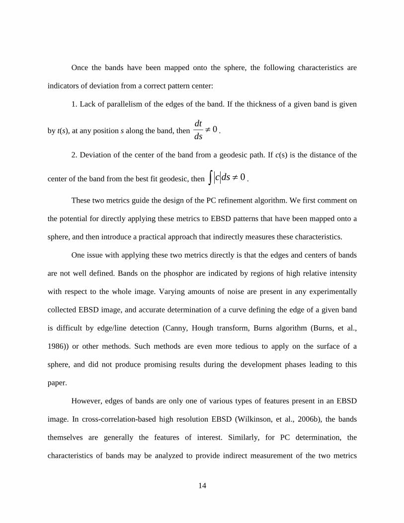


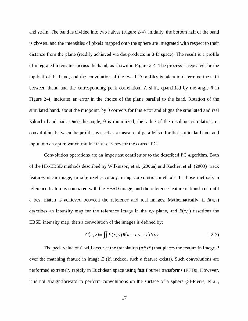


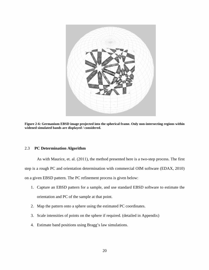


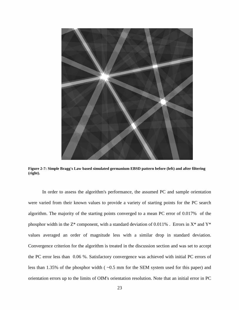

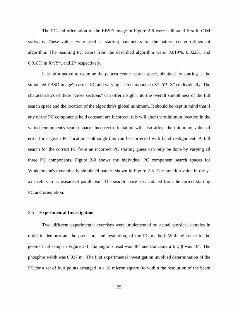
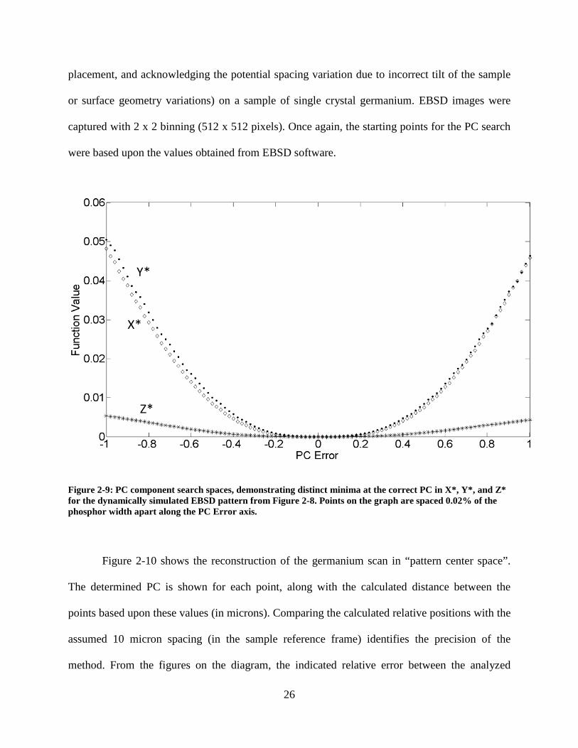


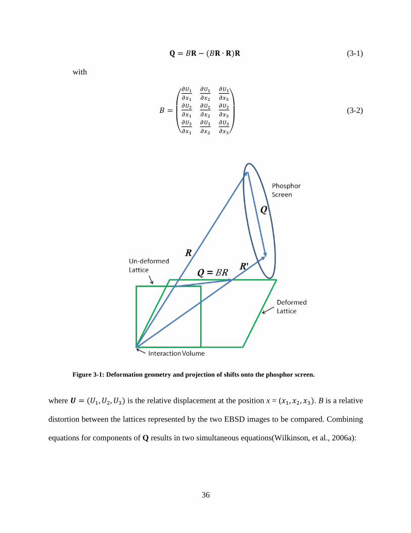


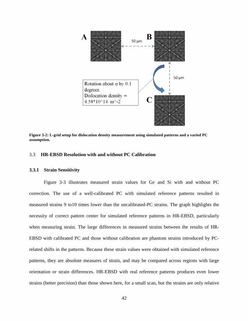
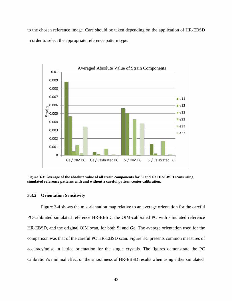


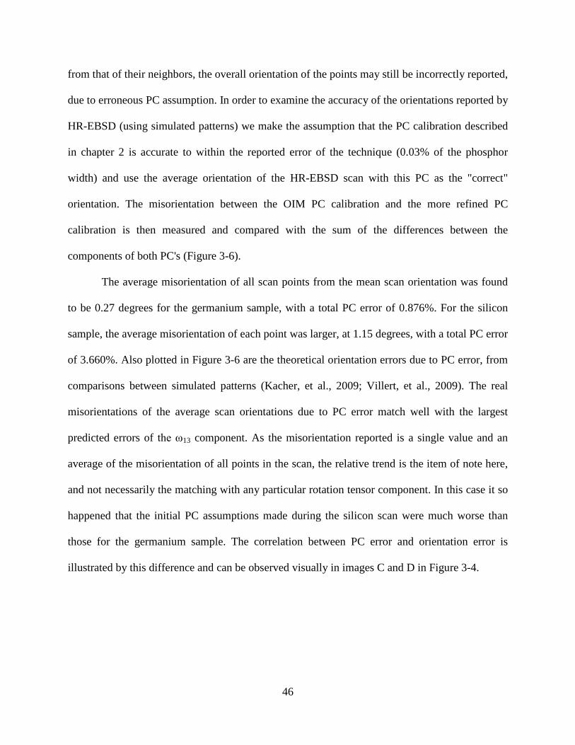


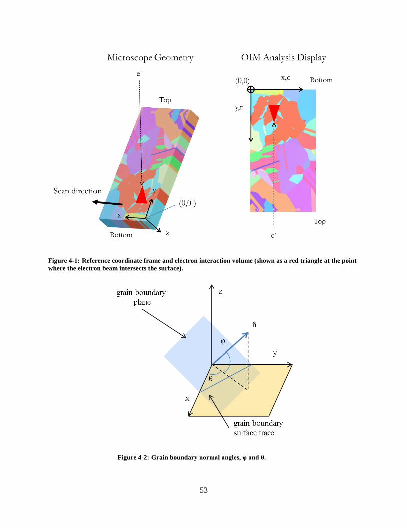

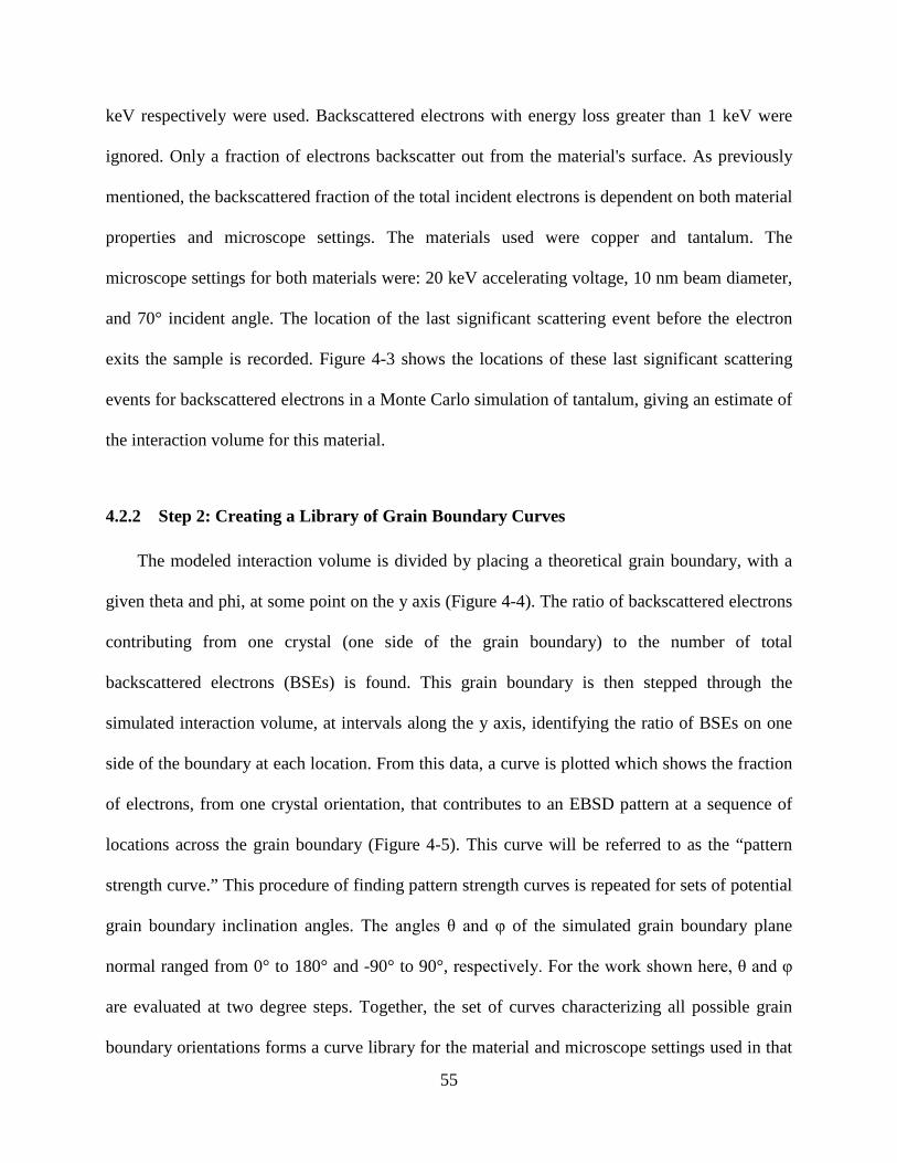

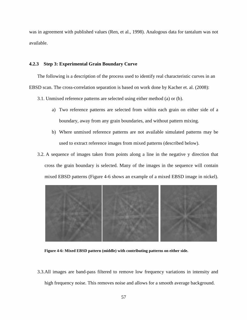

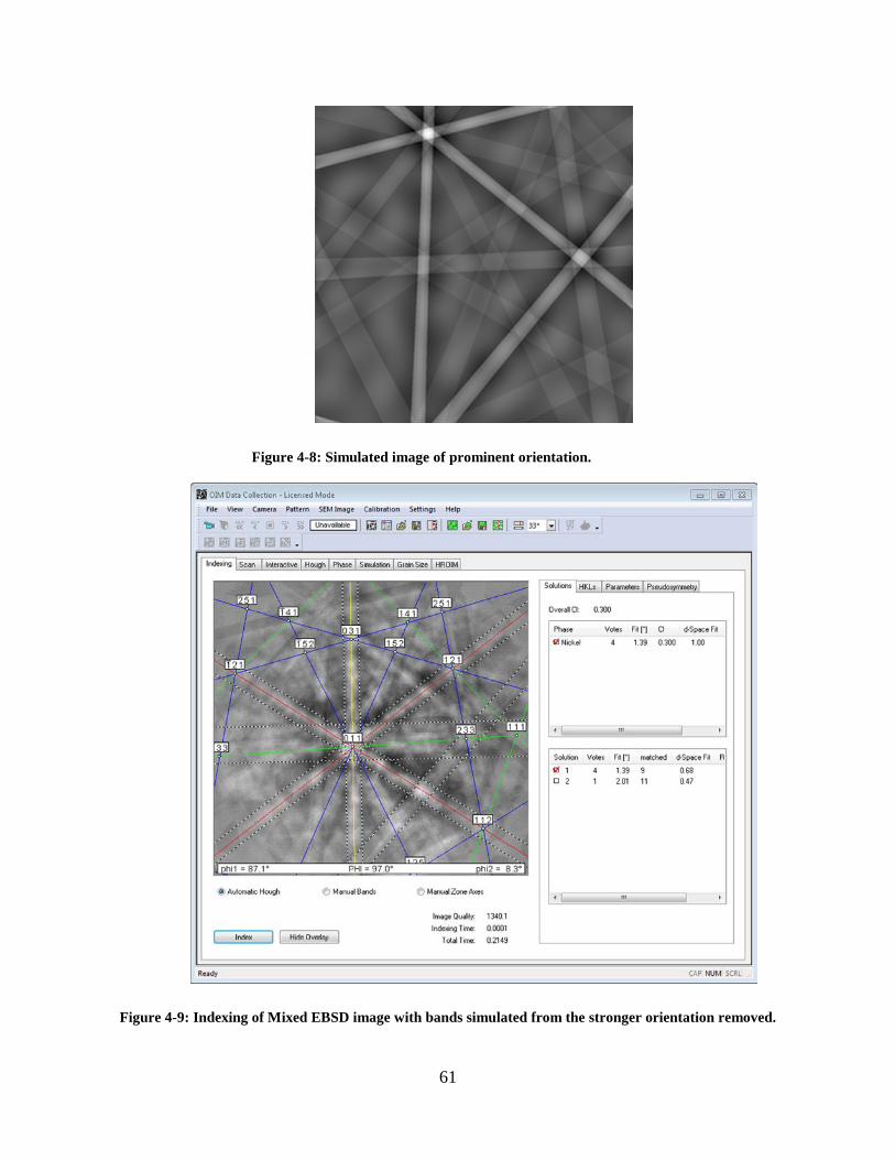

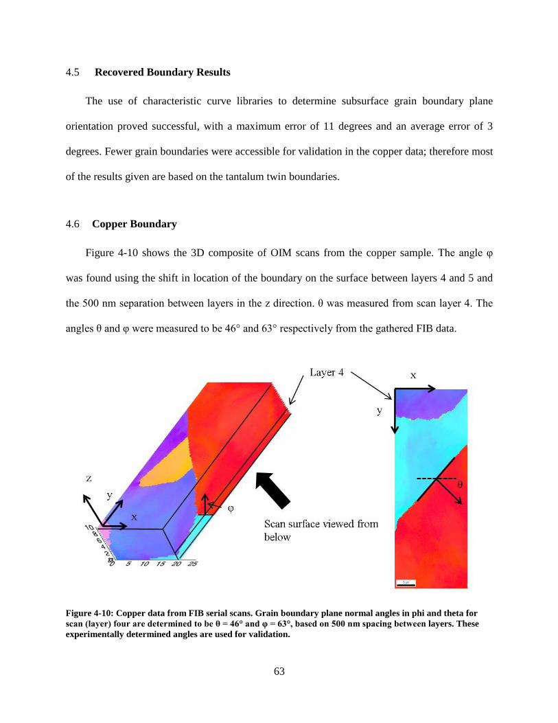


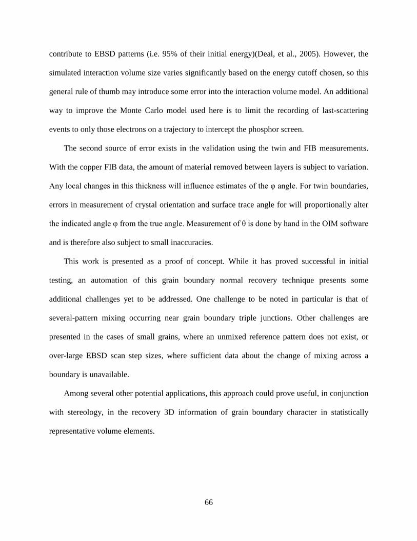


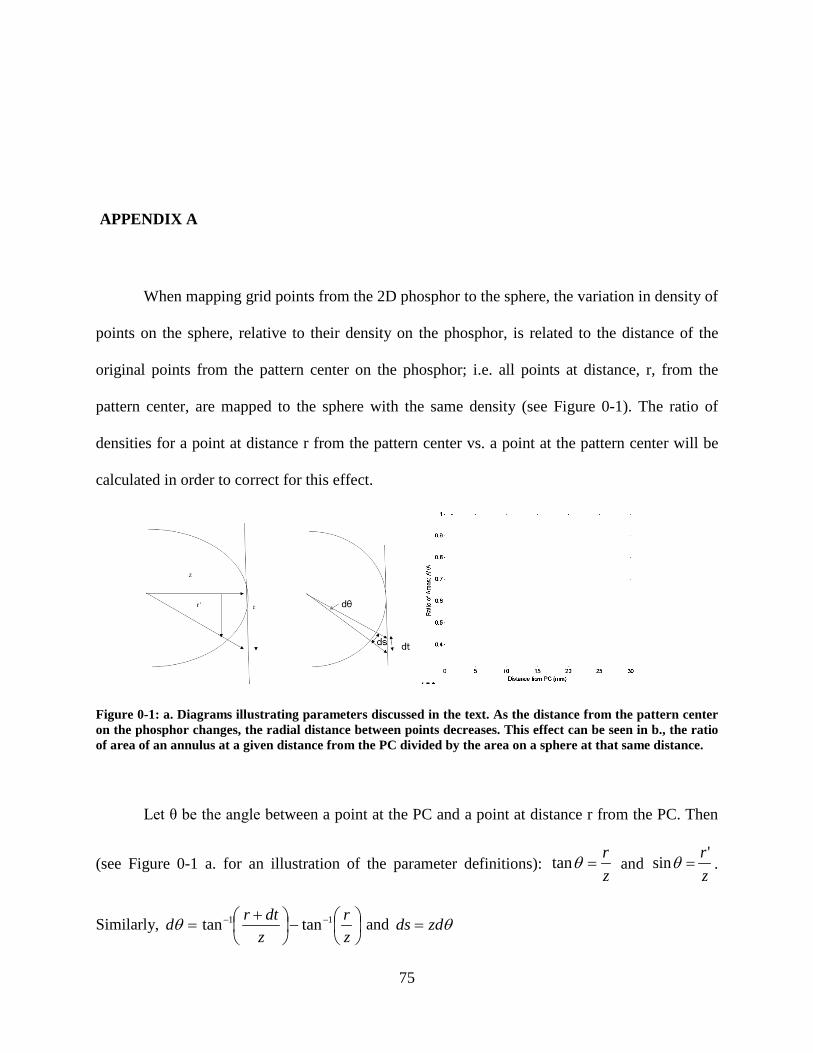


![ELECTRON BACKSCATTER DIFFRACTION CRYSTAL … · 2014. 8. 8. · Electron backscatter diffraction (EBSD) measurement [1,2] is generally very useful in analyzing crystal morphology](https://static.documents.pub/doc/80x56/6020ac1488b59757b674b100/electron-backscatter-diffraction-crystal-2014-8-8-electron-backscatter-diffraction.jpg)
