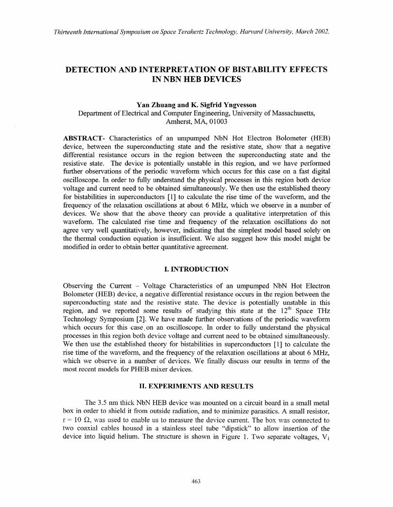
Thirteenth International Symposium on Space Terahertz Technology, Harvard University, March 2002. DETECTION AND INTERPRETATION OF BISTABILITY EFFECTS IN NBN HEB DEVICES Yan Zhuang and K. Sigfrid Yngvesson Department of Electrical and Computer Engineering, University of Massachusetts, Amherst, MA, 01003 ABSTRACT- Characteristics of an umpumped NbN Hot Electron Bolometer (HEB) device, between the superconducting state and the resistive state, show that a negative differential resistance occurs in the region between the superconducting state and the resistive state. The device is potentially unstable in this region, and we have performed further observations of the periodic waveform which occurs for this case on a fast digital oscilloscope. In order to fully understand the physical processes in this region both device voltage and current need to be obtained simultaneously. We then use the established theory for bistabilities in superconductors [1] to calculate the use time of the waveform, and the frequency of the relaxation oscillations at about 6 MHz, which we observe in a number of devices. We show that the above theory can provide a qualitative interpretation of this waveform. The calculated rise time and frequency of the relaxation oscillations do not agree very well quantitatively, however, indicating that the simplest model based solely on the thermal conduction equation is insufficient. We also suggest how this model might be modified in order to obtain better quantitative agreement. I. INTRODUCTION Observing the Current — Voltage Characteristics of an umpumped NbN Hot Electron Bolometer (HEB) device, a negative differential resistance occurs in the region between the superconducting state and the resistive state. The device is potentially unstable in this region, and we reported some results of studying this state at the 12 th Space THz Technology Symposium [2]. We have made further observations of the periodic waveform which occurs for this case , on an oscilloscope. In order to fully understand the physical processes in this region both device voltage and current need to be obtained simultaneously. We then use the established theory for bistabilities in superconductors [1] to calculate the rise time of the waveform, and the frequency of the relaxation oscillations at about 6 MHz, which we observe in a number of devices. We finally discuss our results in terms of the most recent models for PHEB mixer devices. IL EXPERIMENTS AND RESULTS The 3.5 nm thick NbN HEB device was mounted on a circuit board in a small metal box in order to shield it from outside radiation, and to minimize parasitics. A small resistor, r = 10 S2, was used to enable us to measure the device current. The box was connected to t wo coaxial cables housed in a stainless steel tube "dipstick" to allow insertion of the device into liquid helium. The structure is shown in Figure 1. Two separate voltages, V1 463
Transcript
Thirteenth International Symposium on Space Terahertz Technology, Harvard University, March 2002.
DETECTION AND INTERPRETATION OF BISTABILITY EFFECTSIN NBN HEB DEVICES
Yan Zhuang and K. Sigfrid YngvessonDepartment of Electrical and Computer Engineering, University of Massachusetts,
Amherst, MA, 01003
ABSTRACT- Characteristics of an umpumped NbN Hot Electron Bolometer (HEB)device, between the superconducting state and the resistive state, show that a negativedifferential resistance occurs in the region between the superconducting state and theresistive state. The device is potentially unstable in this region, and we have performedfurther observations of the periodic waveform which occurs for this case on a fast digitaloscilloscope. In order to fully understand the physical processes in this region both devicevoltage and current need to be obtained simultaneously. We then use the established theoryfor bistabilities in superconductors [1] to calculate the use time of the waveform, and thefrequency of the relaxation oscillations at about 6 MHz, which we observe in a number ofdevices. We show that the above theory can provide a qualitative interpretation of thiswaveform. The calculated rise time and frequency of the relaxation oscillations do notagree very well quantitatively, however, indicating that the simplest model based solely onthe thermal conduction equation is insufficient. We also suggest how this model might bemodified in order to obtain better quantitative agreement.
I. INTRODUCTION
Observing the Current — Voltage Characteristics of an umpumped NbN Hot ElectronBolometer (HEB) device, a negative differential resistance occurs in the region between thesuperconducting state and the resistive state. The device is potentially unstable in thisregion, and we reported some results of studying this state at the 12
th
Space THzTechnology Symposium [2]. We have made further observations of the periodic waveformwhich occurs for this case , on an oscilloscope. In order to fully understand the physicalprocesses in this region both device voltage and current need to be obtained simultaneously.We then use the established theory for bistabilities in superconductors [1] to calculate therise time of the waveform, and the frequency of the relaxation oscillations at about 6 MHz,which we observe in a number of devices. We finally discuss our results in terms of themost recent models for PHEB mixer devices.
IL EXPERIMENTS AND RESULTS
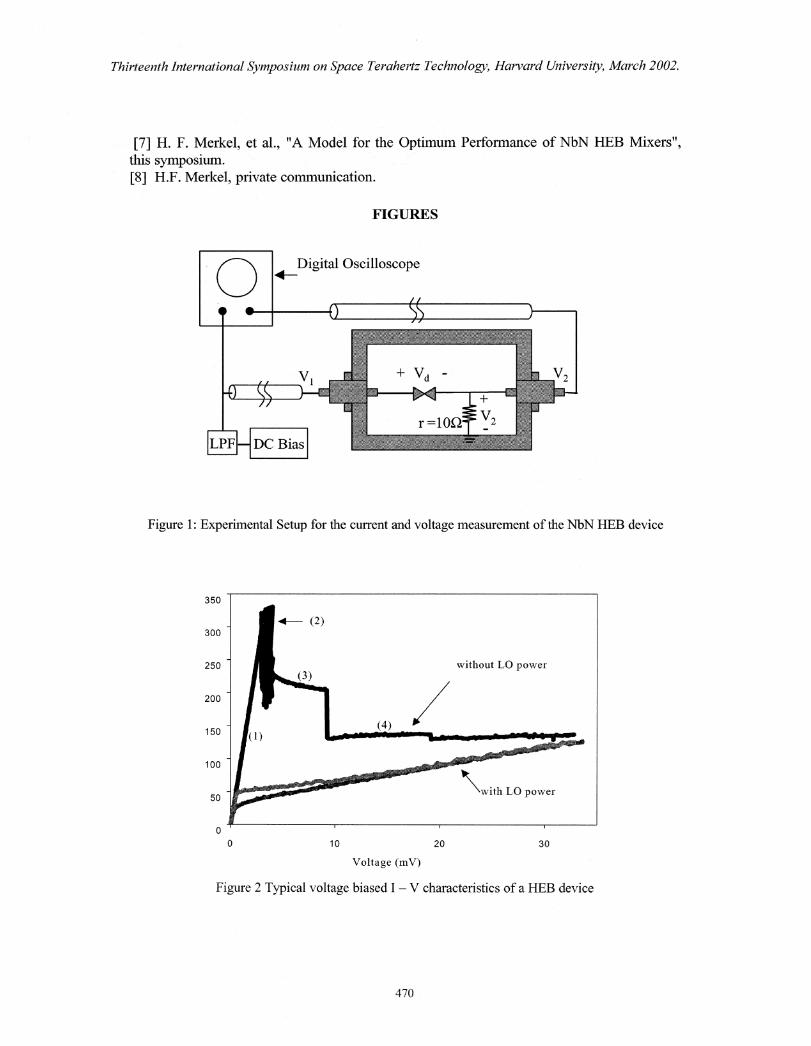
The 3.5 nm thick NbN HEB device was mounted on a circuit board in a small metalbox in order to shield it from outside radiation, and to minimize parasitics. A small resistor,r = 10 S2, was used to enable us to measure the device current. The box was connected totwo coaxial cables housed in a stainless steel tube "dipstick" to allow insertion of thedevice into liquid helium. The structure is shown in Figure 1. Two separate voltages, V1
463
Thirteenth International Symposium on Space Terahertz Technology, Harvard University, March 2002.
and V2, can be measured by connecting each cable to one channel of a digital oscilloscopewhose maximum frequency is about 1 GHz. In this situation both the voltage across thedevice (Vd) and the device current (I d) can be measured simultaneously. This turned out tobe very important for the interpretation of the data
Vd = VI —V2
= V2 /r (2)
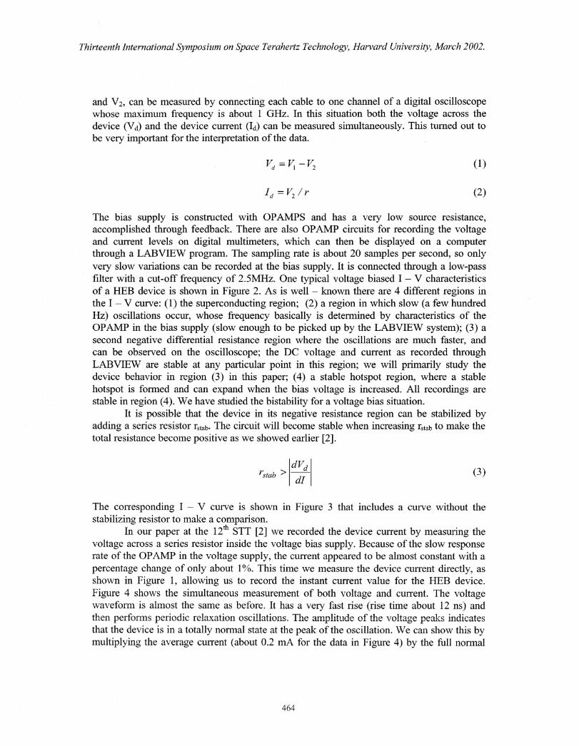
The bias supply is constructed with OPAMPS and has a very low source resistance,accomplished through feedback. There are also OPAMP circuits for recording the voltageand current levels on digital multimeters, which can then be displayed on a computerthrough a LABVIEW program. The sampling rate is about 20 samples per second, so onlyvery slow variations can be recorded at the bias supply. It is connected through a low-passfilter with a cut-off frequency of 2.5MHz. One typical voltage biased I — V characteristicsof a HEB device is shown in Figure 2. As is well — known there are 4 different regions inthe I — V curve: (1) the superconducting region; (2) a region in which slow (a few hundredHz) oscillations occur, whose frequency basically is determined by characteristics of theOPAMP in the bias supply (slow enough to be picked up by the LABVIEW system); (3) asecond negative differential resistance region where the oscillations are much faster, andcan be observed on the oscilloscope; the DC voltage and current as recorded throughLABVIEW are stable at any particular point in this region; we will primarily study thedevice behavior in region (3) in this paper; (4) a stable hotspot region, where a stablehotspot is formed and can expand when the bias voltage is increased. All recordings arestable in region (4). We have studied the bistability for a voltage bias situation.
It is possible that the device in its negative resistance region can be stabilized byadding a series resistor rstab . The circuit will become stable when increasing rstab to make thetotal resistance become positive as we showed earlier [2].
dVd
dlrsta
b > (3)
The corresponding I — V curve is shown in Figure 3 that includes a curve without thestabilizing resistor to make a comparison.
In our paper at the 12th
STT [2] we recorded the device current by measuring thevoltage across a series resistor inside the voltage bias supply. Because of the slow responserate of the OPAMP in the voltage supply, the current appeared to be almost constant with apercentage change of only about 1%. This time we measure the device current directly, asshown in Figure 1, allowing us to record the instant current value for the HEB device.Figure 4 shows the simultaneous measurement of both voltage and current. The voltagewaveform is almost the same as before. It has a very fast rise (rise time about 12 ns) andthen performs periodic relaxation oscillations. The amplitude of the voltage peaks indicatesthat the device is in a totally normal state at the peak of the oscillation. We can show this bymultiplying the average current (about 0.2 mA for the data in Figure 4) by the full normal
464
Thirteenth international Symposium on Space Terahertz Technology, Harvard University, March 2002.
resistance (RN 150 Q) of the device. We find a voltage of 30 mV, which agrees with thepeak voltage amplitude in Figure 4. When the relaxation oscillations die out, the devicereturns to superconducting, as indicated by the voltage across it being zero. Thecorresponding current during the relaxation oscillations used in this estimate is the averagecurrent in the instability region. The current also shows (weaker) relaxation oscillations.When the oscillations vanish, and the device is temporarily back to being superconducting,the current gradually increases, reaches the critical value, and the cycle repeats. Therepetition rate of the waveform increases with increasing bias voltage, as shown in Figure5.
III DISCUSSION
We now discuss the measurement results in terms of a one — dimensional hotspotmodel.
The Superconducting StateIt has been claimed that the main mechanism which determines the critical current
in the superconducting state of an HEB device is vortex pinning. As long as the pinningforce is larger than the Lorenz force, the device remains in the superconducting state. Butour calculation concludes that there are no vortices available in the NbN film of an HEBdevice of a typical size. For example, in the simplest case, we consider a strip with width W= 511m; length L = 1 p.m; thickness d = 4 nm; and total current I -= Ic =500p,A. The x-direction is along the device width. The H field in the x-direction (perpendicular to thecurrent direction) is more or less independent of x, except for at the edges. Although thefield has a singularity at the edges, this singularity is of no consequence when we integratethe field in order to obtain the total flux. We can then estimate that Bx iloHx=1.10I2W=1.2x10 -4 Vs/m2, and the total flux (1)=3x10 -16Vs. However, a vortex must contain aminimum flux of one flux quantum, which is 0 0=2x10-15 Vs. Thus vortices can not exist inthis strip. The critical current is probably determined by depairing of the Cooper pairsrather than by vortex pinning.
Instability RegionIn earlier studies it has been found that the superconductivity can be destroyed by
Joule self — heating even when the transport current is much lower than the critical current[1],[3],[4]. The cooling and heating mechanisms obey the heat balance equation:
Q(T).=
h(T)147 .T)= (1- —T0)
Here Q(T) = jE(T) is the power of the Joule heat released per unit volume. W(T) is thespecific power of heat transfer to the coolant kept at a bath temperature To, h(T) is the heattransfer coefficient, d =A/P, A is the area, and P is the perimeter of the cross section of thespecimen. A bistability occurs when this equation holds for several temperatures, as shown
(4)
(5)
465
h(Tc, )7"c 1
/ 2
To1—
TcP d
1 / 2ic a (9)
Thirteenth International Symposium on Space Terahertz Technology, Harvard University, March 2002.
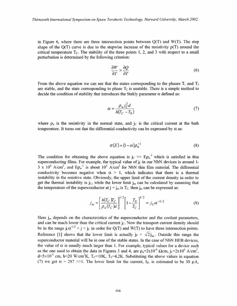
in Figure 6, where there are three intersection points between Q(T) and W(T). The stepshape of the Q(T) curve is due to the stepwise increase of the resistivity p(T) around thecritical temperature Tc. The stability of the three points 1, 2, and 3 with respect to a smallperturbation is determined by the following criterion:
aw aQ aT a T
From the above equation we can see that the states corresponding to the phases T 1 and T3
are stable, and the state corresponding to phase T2 is unstable. There is a simple method todecide the condition of stability that introduces the Stekly parameter a defined as:
• 2 dPidc a=
where IN is the resistivity in the normal state, and jc is the critical current at the bathtemperature. It turns out that the differential conductivity can be expressed by a as
a (E) = (1— ce)p -n-1
(8)
The condition for obtaining the above equation is jc >> Ep ti4 which is satisfied in thin
superconducting films. For example, the typical value of jc in our NbN devices is around 1-3 x 10⁶ A/cm2 , and EN-I is about 105 Aicm2 for NbN thin film material. The differentialconductivity becomes negative when a > 1, which indicates that there is a thermalinstability in the resistive state. Obviously, the upper limit of the current density in order toget the thermal instability is jc, while the lower limit i n can be calculated by assuming thatthe temperature of the superconductor at j = jm is Tc ; then jm can be expressed as:
(6)
41 T(7)
Here jm depends on the characteristics of the superconductor and the coolant parameters,and can be much lower than the critical current jc. Now the transport current density shouldbe in the range jca
2-1 < j < jc in order for Q(T) and W(T) to have three intersection points.
Reference [1] shows that the lower limit is actually jp = . Outside this range thesuperconductor material will be in one of the stable states. In the case of NbN HEB devices,the value of a is usually much larger than 1. For example, typical values for a device suchas the one used to obtain the data in Figures 3 and 4, are p n=2x10⁻⁴ Clcm, jc=2x10⁶ A/c'm2,d=5x10-5 cm, h=20 W/cm2K, Tc=10K, T 0=4.2K. Substituting the above values in equation(7) we get a = 287 >>1. The lower limit for the current, Ip, is estimated to be 30 [tA,
466
Thirteenth International Symposium on Space Terahertz Technology, Harvard University, March 2002.
whereas Ic = 400 [EA. The bistability is thus potentially very strong. We can interpret thebehavior of NbN HEB devices that we observed in Figure 4 in terms of propagation ofswitching waves, which describes the movement of the domain walls between the twostable states: superconducting and normal states. The domain wall moves in one directionwhen transforming from one stable state to the other, or vice versa, depending on the valueof j. The velocity c of the propagation can be expressed as in [5];
c(i)= (1+ 0.561a -1.45 )W -1)1-,64- (10)
M = cd 2 -1+ -i 1- i (11)2 2
Here c(i)= v/vh, vh= L/th, where L and th are the characteristic thermal length and time, andjijc is the dimensionless current density. The c value as a function of dimensionless
current i is plotted in Figure 7. We also estimate vh 1.04 cm/sec. Our interpretation of thedevice behavior in region (3) can then be summarized as follows:
1) After j, has been exceeded, a normal domain spreads with an initialnormalized velocity c = 24. The expansion will slow as the resistance grows, and thecurrent decreases, until the normal domain reaches the contacts. The average velocity
5during the initial expansion can be estimated to be 10 x v h = 10 cm/s. The initial velocityis so high that it is close to the sound velocity in the film, which should act as an ultimatespeed limit. The estimated time for a domain to cover half the length of the device is about.5 ns, a very short time, while we measured a value of 12 ns. The initial rise time is,however, also influenced by the response time of our measurement system, which wechecked by a measurement using a fast (6 ns rise time) pulse generator substituting for theHEB device. The rise time was found to be 15 ns which confirms that we could not havemeasured the rise time of the HEB device waveform if it had been as fast as .5 ns.
After the initial transient, the voltage and current oscillate around an average currentof about 200 RA. From the bistability theory, we would expect that for j > jp, the domainwould grow with increasing velocity until it reaches the contacts, and R = R. In region (3)there is not enough power available to sustain a stable hot spot, and the current hasmeanwhile decreased below jp, which reverses the sign of the velocity, and the domainthen decreases in size; the current subsequently increases above jp again, leading to thedomain oscillating back and forth until the device goes superconducting, etc.. Thefrequency of these relaxation oscillations can be found by estimating the time required forthe domain to expand through about half the length of the device, and back again. Weassume that the oscillations are sinusoidal. Also, the measured average current is 200 1.1,Arather than the expected value of 30 p.A, based on jp, and a = 290. The velocity curve forthis larger average current value has also been plotted in Figure 4. It corresponds to a = 10.If we assume that the oscillations occur around this current point, and use the measuredpeak current amplitude from Figure 4, we find a relaxation oscillation frequency of about60 MHz, with a period of 16 ns. Instead, we measure the period of the oscillation to beroughly 160 ns, or a frequency of 6 MHz. In addition to the higher than expected averagecurrent, this seems to give us pretty clear evidence that one must include further physical
467
Thirteenth international Symposium on Space Terahertz Technology, Harvard University, March 2002.
effects in the calculation of the propagation speed than the purely thermal effects (lateralthermal conduction and heat transfer to the substrate) which were included in the abovecalculation. Possible such effects are:
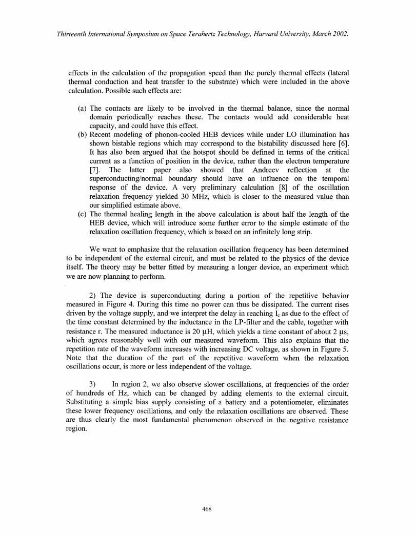
(a) The contacts are likely to be involved in the thermal balance, since the normaldomain periodically reaches these. The contacts would add considerable heatcapacity, and could have this effect.
(b) Recent modeling of phonon-cooled HEB devices while under LO illumination hasshown bistable regions which may correspond to the bistability discussed here [6].It has also been argued that the hotspot should be defined in terms of the criticalcurrent as a function of position in the device, rather than the electron temperature[7]. The latter paper also showed that Andreev reflection at thesuperconducting/normal boundary should have an influence on the temporalresponse of the device. A very preliminary calculation [8] of the oscillationrelaxation frequency yielded 30 MHz, which is closer to the measured value thanour simplified estimate above.,
(c) The thermal healing length in the above calculation is about half the length of theHEB device, which will introduce some further error to the simple estimate of therelaxation oscillation frequency, which is based on an infinitely long strip.
We want to emphasize that the relaxation oscillation frequency has been determinedto be independent of the external circuit, and must be related to the physics of the deviceitself. The theory may be better fitted by measuring a longer device, an experiment whichwe are now planning to perform.
2) The device is superconducting during a portion of the repetitive behaviormeasured in Figure 4. During this time no power can thus be dissipated. The current risesdriven by the voltage supply, and we interpret the delay in reaching I as due to the effect ofthe time constant determined by the inductance in the LP-filter and the cable, together withresistance r. The measured inductance is 20 !AI, which yields a time constant of about 2 [Is,which agrees reasonably well with our measured waveform. This also explains that therepetition rate of the waveform increases with increasing DC voltage, as shown in Figure 5.Note that the duration of the part of the repetitive waveform when the relaxationoscillations occur, is more or less independent of the voltage.
3) In region 2, we also observe slower oscillations, at frequencies of the orderof hundreds of Hz, which can be changed by adding elements to the external circuit.Substituting a simple bias supply consisting of a battery and a potentiometer, eliminatesthese lower frequency oscillations, and only the relaxation oscillations are observed. Theseare thus clearly the most fundamental phenomenon observed in the negative resistanceregion.
468
Thirteenth International Symposium on Space Terahertz Technology, Harvard University, March 2002.
Consequences for device behavior in active mixer operationThe model we have used to estimate the rate at which a hot-spot domain can vary its
size could also be used to analyze device models in the stable state, where LO power isapplied to bring the differential conductivity to positive values. The modeling required foractual HEB mixer operation is likely to be much more complex, as shown in papers byMerkel et al. [6,7]. The advantage of our approach is that it is possible to test the models forthe bistable regions and for the temporal response of hotspots with relatively simplemeasurements. Our experiments also detect higher frequencies in the GHz range, when theHEB device is measured in the bistable region through a low-noise cooled HEMTamplifier.
IV. CONCLUSION
In this paper we measured the voltage and the current of the NbN HEB devicesimultaneously in the bistability region. We conclude that no vortices can exist in a typicalNbN HEB strip. The transition between the superconducting state and the normal state wasinterpreted qualitatively as the propagation of a switching wave. The calculated relaxationoscillation frequency based on the domain velocity is about ten times higher with themeasured result. We expect that use of a more detailed model of the device will result incloser quantitative agreement with measurements in the future. Also, measurements onlonger devices, which we plan to carry out, should facilitate better agreement betweentheory and experiment.
ACKNOWLEDGEMENTS
We would like to acknowledge stimulating discussions with Dr. Harald Merkel ofChalmers University of Technology. We would also like to acknowledge support fromNASA Contract NAS1-01058 from NASA Langley Research Center.
REFERENCES
[1] A.VI. Gurevich and R.G. Mints, "Self-Heating in Normal Metals and Superconductors,"Rev. Mod. Physics, 59, 941 (1987).[2] Y. Zhuang and K.S. Yngvesson, "Negative Resistance Effects in NbN HEB devices,"12 th Intern. Symp. Space THz Technol, San Diego, CA, Feb. 2001, pp. 143-153[3] V.A. Altov, V.B. Zenkevitch, M.G. Kremlev, and V.V. Sytchev, "Stabilization ofSuperconducting Magnetic Systems (Plenum, New York)", 1977.[4] V.L. Newhouse, Applied Superconductivity (Wiley, New York), 1964[5] L. Dresner, "Analytic Solution for the propagation velocity in superconductingcomposites", IEEE Trans. Magn. 15, 328, 1979[6] H.F. Merkel, P. Khosropanah, KS. Yngvesson, S. Cherednichenko, M. Kroug, A.Adam, and E.L. Kollberg, "An Active Zone Small Signal Model For Hot ElectronBolometric Mixers,", 12 th Intern. Symp. Space THz Technol, San Diego, CA, Feb. 2001,pp. 67-74
469
Digital Oscilloscope4—
ifgW•
—I DC Bias ,;(,),‘ A ArEta=1„PW140 datEOMITCYS 'A
10 20 30
without LO power
with LO povver
350
300
250
200
150
100
50
Thirteenth international Symposium on Space Terahertz Technology, Harvard University, March 2002.
[7] H. F. Merkel, et al.., "A Model for the Optimum Performance of NbN HEB Mixers",this symposium.[8] H.F. Merkel, private communication.
FIGURES
Figure 1: Experimental Setup for the current and voltage measurement of the NbN 11E3 device
Voltage (mV)
Figure 2 Typical voltage biased I — V characteristics of a HEB device
470
Thirteenth international Symposium on Space Terahertz Technology, Harvard University, March 2002.
5 10 15 20 25
Voltage (mV)
Figure 3: I —V characteristics of a HEB device with stabilizing resistor
Figure 4: Voltage and Current waveform in the bistability region of the HEB device
471
Temperature (K)
W,Q
6 8 10 12 14
580
560-
540 -
520 -
500 --
480 -
460-
440 -
420 -
400 -
380
Thirteenth International Symposium on Space Terahertz Technology, Harvard University, March 2002.
Voltage (mV)
Figure 5: Repetition frequency as a function Figure 6: W and Q curves as aof the bias voltage function of temperature
Initial transientfrom j = c
1p2 04
25
20 -
15 -
10 -
5 -
0
-5 0.0 ip1 0.2
I
I
Expansion(c > 0)Contraction(c < 0)
0.6 0.8 1.0
Relalcatiovv oscil‘atiovvs(IF 10
Current ( jc)
Figure 7: c(i) = vivh as a function of i=j/jc for a = 290 and a=10