Developed by Toby @ IMUS Laboratory, 2016 Attribution-NonCommercial-NoDerivs 3.0 Hong Kong (CC BY-NC-ND 3.0 HK) 4 Port USB Power Bank With 4A SAB-CHRG Technology Output 5V 1A (Dual Protection) / 2A (With OTG) / 2A / 3A (3.2A OC) Charging Input 5V 1A - 4A(Max), With SMART CHARGING CONTROLLER Simple Introduction This Powerbank consist of 4 USB Port. Port 1: 5V 1A Dual Protection with Current limit System and Short circuit Protection. Port 2: 5V 2A With OTG Function connected to the Power Bank Port 3 (For Phone) Port 3: 5V 2A With OTG Function connected to the Power Bank Port 2 (For OTG USB) Port 4: 5V 3A High Current Output for Tablet Controlled by ATmega328P-AU Micro-controller, high charging current with SAB-CHRG (Stand Alone Battery CHaRGing System) Technology can be achieved. Overall Wiring Diagram *See Appendix for this diagram in FULL HD
Transcript
Developed by Toby @ IMUS Laboratory, 2016
Attribution-NonCommercial-NoDerivs 3.0 Hong Kong (CC BY-NC-ND 3.0 HK)
4 Port USB Power Bank With 4A SAB-CHRG Technology Output 5V 1A (Dual Protection) / 2A (With OTG) / 2A / 3A (3.2A OC) Charging Input 5V 1A - 4A(Max), With SMART CHARGING CONTROLLER
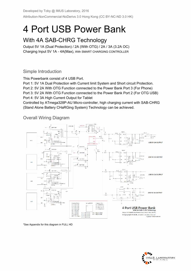
Simple Introduction This Powerbank consist of 4 USB Port. Port 1: 5V 1A Dual Protection with Current limit System and Short circuit Protection. Port 2: 5V 2A With OTG Function connected to the Power Bank Port 3 (For Phone) Port 3: 5V 2A With OTG Function connected to the Power Bank Port 2 (For OTG USB) Port 4: 5V 3A High Current Output for Tablet Controlled by ATmega328P-AU Micro-controller, high charging current with SAB-CHRG (Stand Alone Battery CHaRGing System) Technology can be achieved.
Overall Wiring Diagram
*See Appendix for this diagram in FULL HD
Developed by Toby @ IMUS Laboratory, 2016
Attribution-NonCommercial-NoDerivs 3.0 Hong Kong (CC BY-NC-ND 3.0 HK)
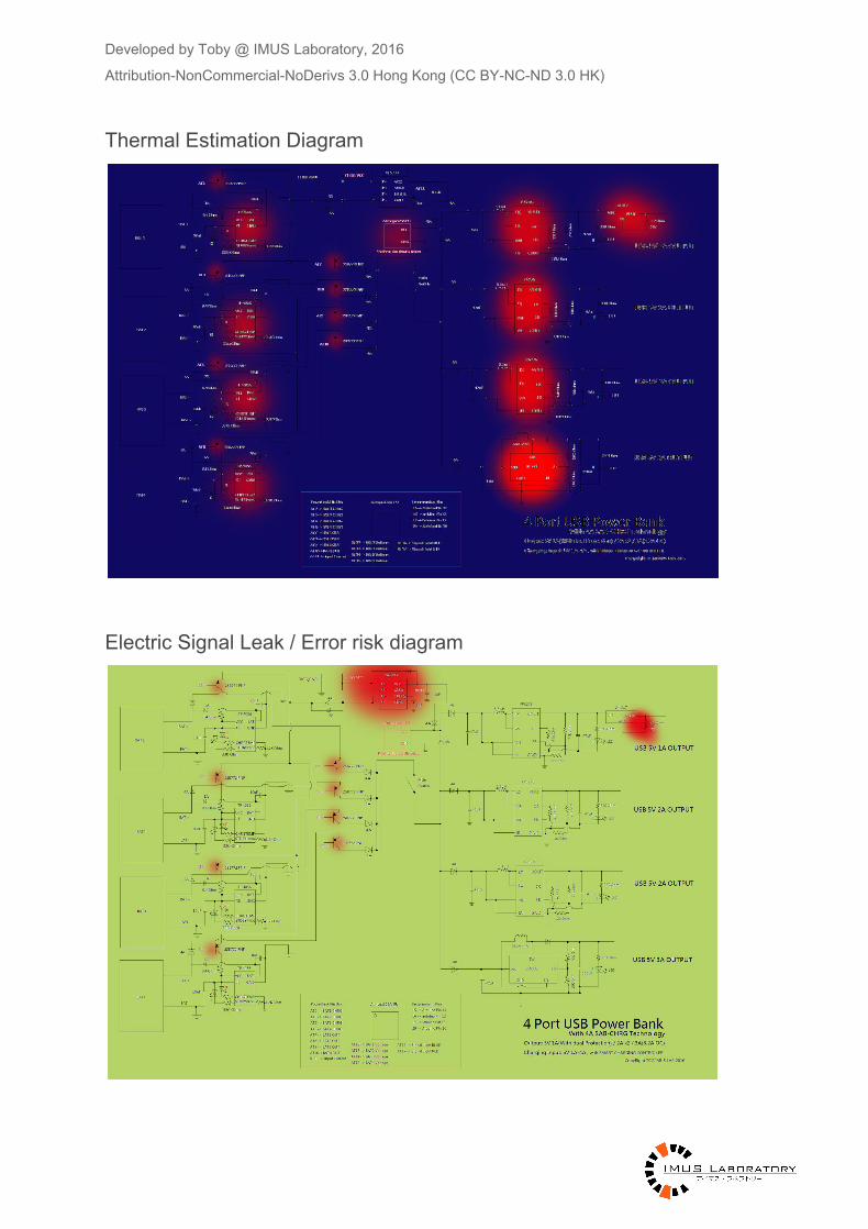
Thermal Estimation Diagram
Electric Signal Leak / Error risk diagram
Developed by Toby @ IMUS Laboratory, 2016
Attribution-NonCommercial-NoDerivs 3.0 Hong Kong (CC BY-NC-ND 3.0 HK)
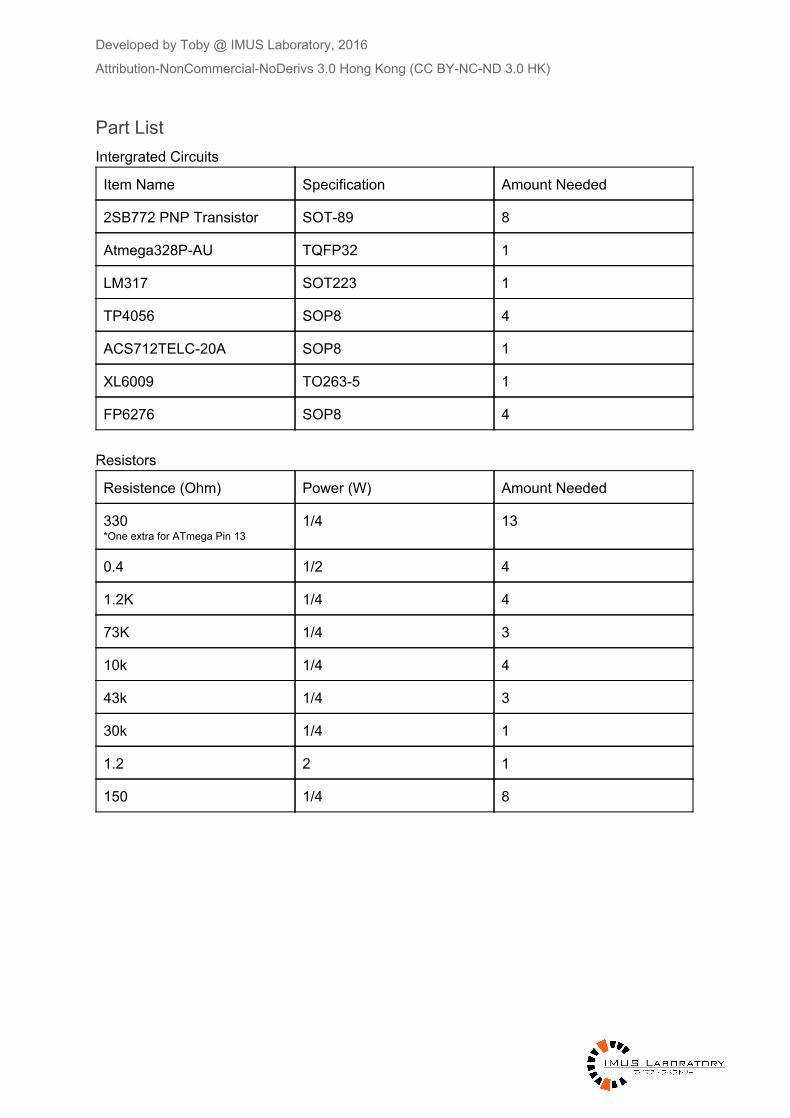
Part List Intergrated Circuits
Item Name Specification Amount Needed
2SB772 PNP Transistor SOT-89 8
Atmega328P-AU TQFP32 1
LM317 SOT223 1
TP4056 SOP8 4
ACS712TELC-20A SOP8 1
XL6009 TO263-5 1
FP6276 SOP8 4
Resistors
Resistence (Ohm) Power (W) Amount Needed
330 *One extra for ATmega Pin 13
1/4 13
0.4 1/2 4
1.2K 1/4 4
73K 1/4 3
10k 1/4 4
43k 1/4 3
30k 1/4 1
1.2 2 1
150 1/4 8
Developed by Toby @ IMUS Laboratory, 2016
Attribution-NonCommercial-NoDerivs 3.0 Hong Kong (CC BY-NC-ND 3.0 HK)
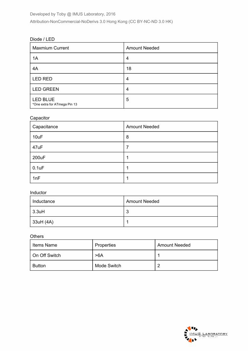
Diode / LED
Maxmium Current Amount Needed
1A 4
4A 18
LED RED 4
LED GREEN 4
LED BLUE *One extra for ATmega Pin 13
5
Capacitor
Capacitance Amount Needed
10uF 8
47uF 7
200uF 1
0.1uF 1
1nF 1
Inductor
Inductance Amount Needed
3.3uH 3
33uH (4A) 1
Others
Items Name Properties Amount Needed
On Off Switch >6A 1
Button Mode Switch 2
Developed by Toby @ IMUS Laboratory, 2016
Attribution-NonCommercial-NoDerivs 3.0 Hong Kong (CC BY-NC-ND 3.0 HK)
Modes The Power Bank comes in few different modes
Modes releated to Power Bank Charging
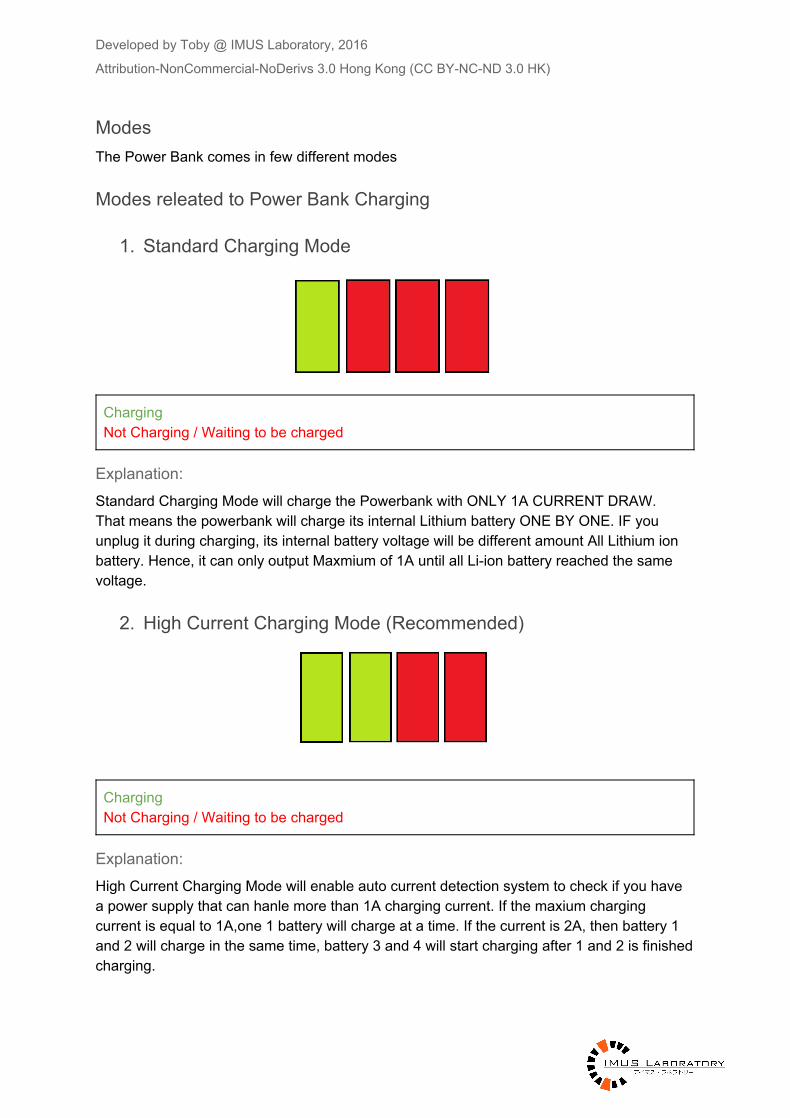
1. Standard Charging Mode
Charging Not Charging / Waiting to be charged
Explanation: Standard Charging Mode will charge the Powerbank with ONLY 1A CURRENT DRAW. That means the powerbank will charge its internal Lithium battery ONE BY ONE. IF you unplug it during charging, its internal battery voltage will be different amount All Lithium ion battery. Hence, it can only output Maxmium of 1A until all Li-ion battery reached the same voltage.
2. High Current Charging Mode (Recommended)
Charging Not Charging / Waiting to be charged
Explanation: High Current Charging Mode will enable auto current detection system to check if you have a power supply that can hanle more than 1A charging current. If the maxium charging current is equal to 1A,one 1 battery will charge at a time. If the current is 2A, then battery 1 and 2 will charge in the same time, battery 3 and 4 will start charging after 1 and 2 is finished charging.
Developed by Toby @ IMUS Laboratory, 2016
Attribution-NonCommercial-NoDerivs 3.0 Hong Kong (CC BY-NC-ND 3.0 HK)
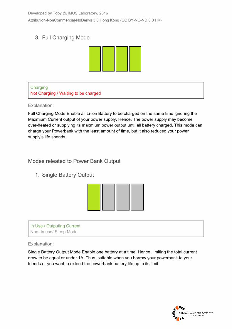
3. Full Charging Mode
Charging Not Charging / Waiting to be charged
Explanation: Full Charging Mode Enable all Li-ion Battery to be charged on the same time ignoring the Maxmium Current output of your power supply. Hence, The power supply may become over-heated or supplying its maxmium power output until all battery charged. This mode can charge your Powerbank with the least amount of time, but it also reduced your power supply’s life spends.
Modes releated to Power Bank Output
1. Single Battery Output
In Use / Outputing Current Non- in use/ Sleep Mode
Explanation: Single Battery Output Mode Enable one battery at a time. Hence, limiting the total current draw to be equal or under 1A. Thus, suitable when you borrow your powerbank to your friends or you want to extend the powerbank battery life up to its limit.
Developed by Toby @ IMUS Laboratory, 2016
Attribution-NonCommercial-NoDerivs 3.0 Hong Kong (CC BY-NC-ND 3.0 HK)
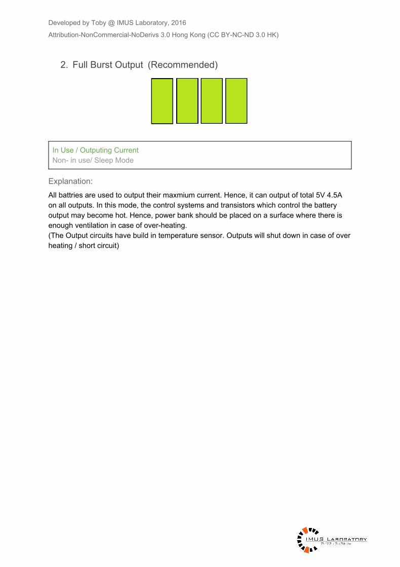
2. Full Burst Output (Recommended)
In Use / Outputing Current Non- in use/ Sleep Mode
Explanation: All battries are used to output their maxmium current. Hence, it can output of total 5V 4.5A on all outputs. In this mode, the control systems and transistors which control the battery output may become hot. Hence, power bank should be placed on a surface where there is enough ventilation in case of over-heating. (The Output circuits have build in temperature sensor. Outputs will shut down in case of over heating / short circuit)
Developed by Toby @ IMUS Laboratory, 2016
Attribution-NonCommercial-NoDerivs 3.0 Hong Kong (CC BY-NC-ND 3.0 HK)
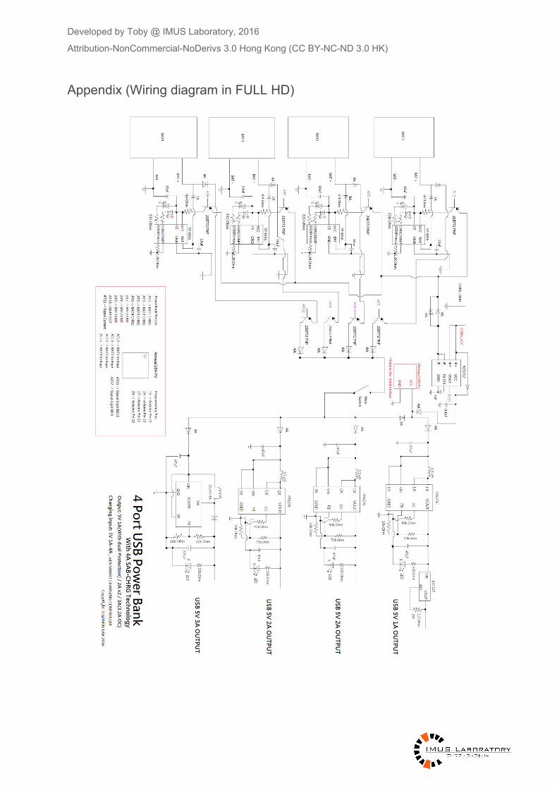
Appendix (Wiring diagram in FULL HD)
Developed by Toby @ IMUS Laboratory, 2016
Attribution-NonCommercial-NoDerivs 3.0 Hong Kong (CC BY-NC-ND 3.0 HK)
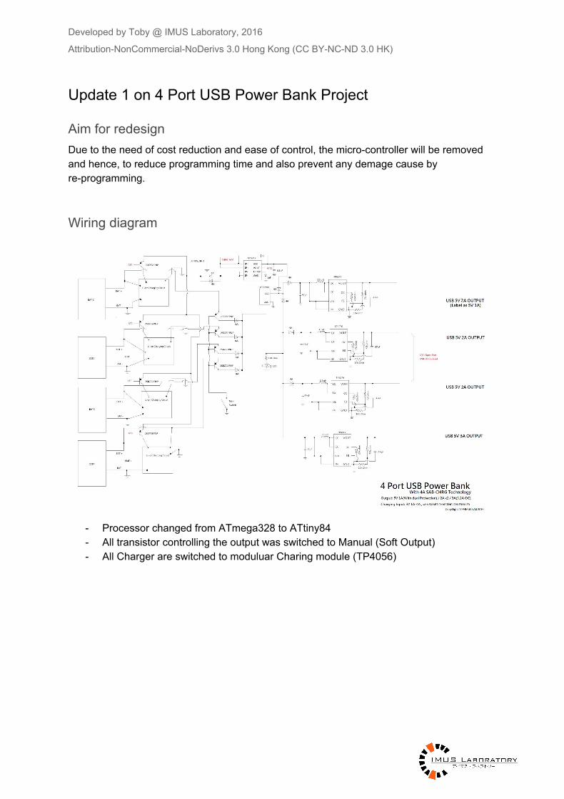
Update 1 on 4 Port USB Power Bank Project
Aim for redesign Due to the need of cost reduction and ease of control, the micro-controller will be removed and hence, to reduce programming time and also prevent any demage cause by re-programming.
Wiring diagram
- Processor changed from ATmega328 to ATtiny84 - All transistor controlling the output was switched to Manual (Soft Output) - All Charger are switched to moduluar Charing module (TP4056)
Developed by Toby @ IMUS Laboratory, 2016
Attribution-NonCommercial-NoDerivs 3.0 Hong Kong (CC BY-NC-ND 3.0 HK)
Update 2 on 8 Port USB Power Bank Project
Aim of complete redesign The old concept is too complicated to make or manufacture. We need a power bank that is so powerful and easy to make (i.e. PCB and SMT based). Hence, I added 4 more ports (In which they come from the same module of the 4 port usb power bank project on the original planning. The project is now renamed as “Eletochondrion” as it is a symbol of “Power House”.
Convertor Module (AKA Quad Port Voltage Step Up Module)
<Top View>
<Bottom View>
Board Information FP6276B x4 3.3uH Inductor x1 0.22, 47 uF Capacitor 73.2k, 32k , 10k, 330 Ohm Resistors 2A dioide (Optional and Experimental) x1 Dual Layer USB Port (Female) x2
** Two of the above modules will be used in ONE Power Bank ** Maximum Output Power of each port suppose to be 5V 2.0A (10W). When all port are drawing 2A, the system may lower the current for each port down to 1.5A due to safty and heating issue.
Developed by Toby @ IMUS Laboratory, 2016
Attribution-NonCommercial-NoDerivs 3.0 Hong Kong (CC BY-NC-ND 3.0 HK)
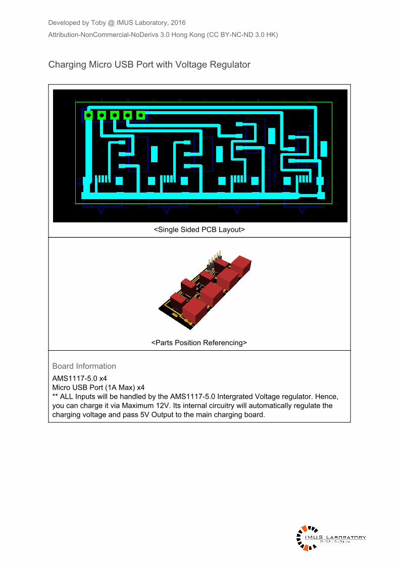
Charging Micro USB Port with Voltage Regulator
<Single Sided PCB Layout>
<Parts Position Referencing>
Board Information AMS1117-5.0 x4 Micro USB Port (1A Max) x4 ** ALL Inputs will be handled by the AMS1117-5.0 Intergrated Voltage regulator. Hence, you can charge it via Maximum 12V. Its internal circuitry will automatically regulate the charging voltage and pass 5V Output to the main charging board.
Developed by Toby @ IMUS Laboratory, 2016
Attribution-NonCommercial-NoDerivs 3.0 Hong Kong (CC BY-NC-ND 3.0 HK)
Minor Modifications One more PCB will be splited from the original 3 boards. Hence, there will be intotal 4 type of PCB inside the Power Bank. Here are the modification in details:
Original
Voltage Step Up Module x2 Charging Managment, LED display array, Main CHRG Port Module x1 Stand Alone Battery Charging Port Board With Voltage Regulator x1
New
Voltage Step Up Module x2 Charging Managment and LED display array x1 Stand Alone Battery Charging Port Board With Current limiting resistors x1 Universal Voltage & Current Input Regulator Port Board x1 (Input Voltage between 6 to 12v, Overall power = 20W (Or 5V 4A))
Developed by Toby @ IMUS Laboratory, 2016
Attribution-NonCommercial-NoDerivs 3.0 Hong Kong (CC BY-NC-ND 3.0 HK)
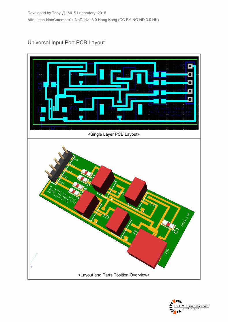
Universal Input Port PCB Layout
<Single Layer PCB Layout>
<Layout and Parts Position Overview>
Developed by Toby @ IMUS Laboratory, 2016
Attribution-NonCommercial-NoDerivs 3.0 Hong Kong (CC BY-NC-ND 3.0 HK)
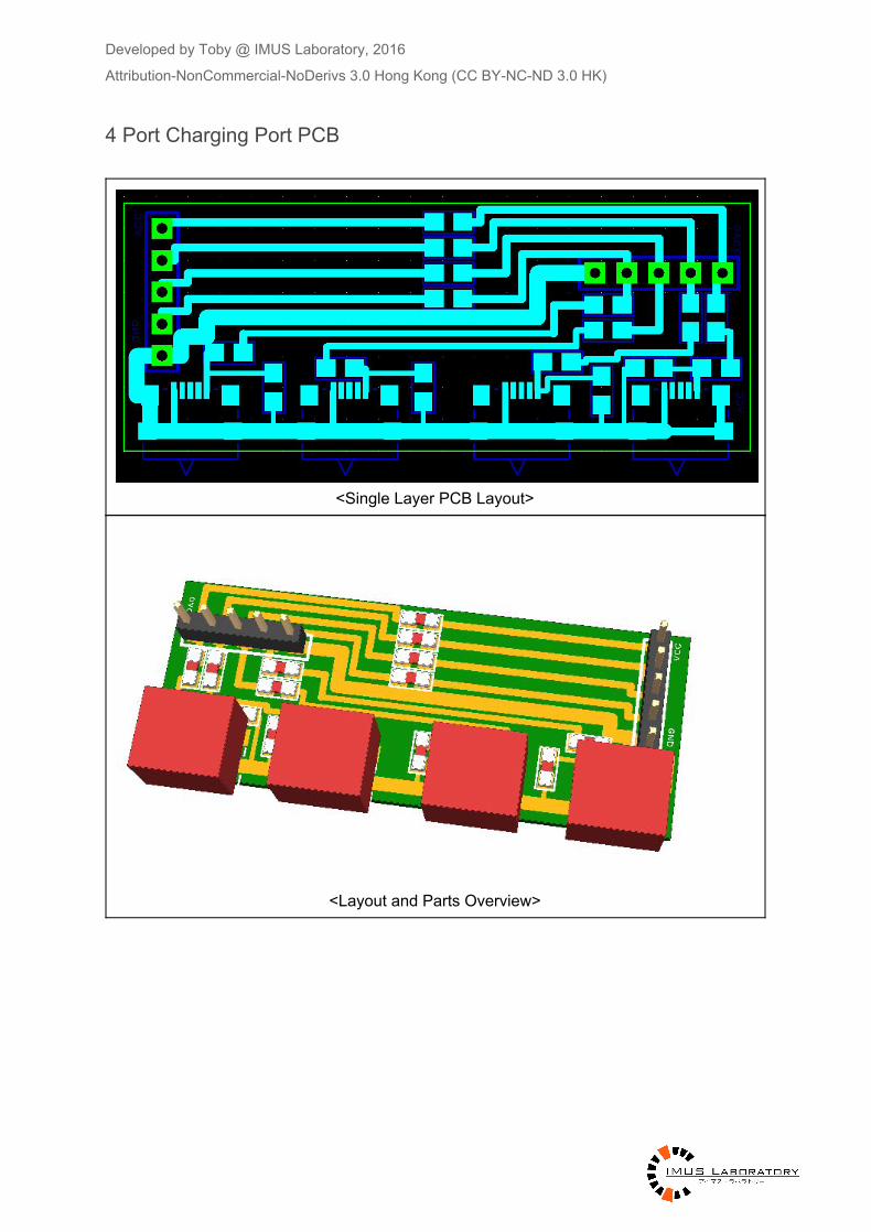
4 Port Charging Port PCB
<Single Layer PCB Layout>
<Layout and Parts Overview>
Developed by Toby @ IMUS Laboratory, 2016
Attribution-NonCommercial-NoDerivs 3.0 Hong Kong (CC BY-NC-ND 3.0 HK)
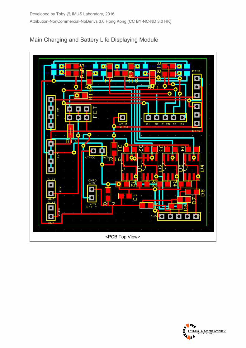
Main Charging and Battery Life Displaying Module
<PCB Top View>
Developed by Toby @ IMUS Laboratory, 2016
Attribution-NonCommercial-NoDerivs 3.0 Hong Kong (CC BY-NC-ND 3.0 HK)
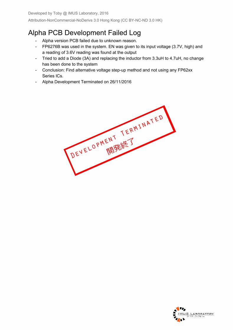
Alpha PCB Development Failed Log - Alpha version PCB failed due to unknown reason. - FP6276B was used in the system. EN was given to its input voltage (3.7V, high) and
a reading of 3.6V reading was found at the output - Tried to add a Diode (3A) and replacing the inductor from 3.3uH to 4.7uH, no change
has been done to the system - Conclusion: Find alternative voltage step-up method and not using any FP62xx
Series ICs. - Alpha Development Terminated on 26/11/2016
Developed by Toby @ IMUS Laboratory, 2016
Attribution-NonCommercial-NoDerivs 3.0 Hong Kong (CC BY-NC-ND 3.0 HK)
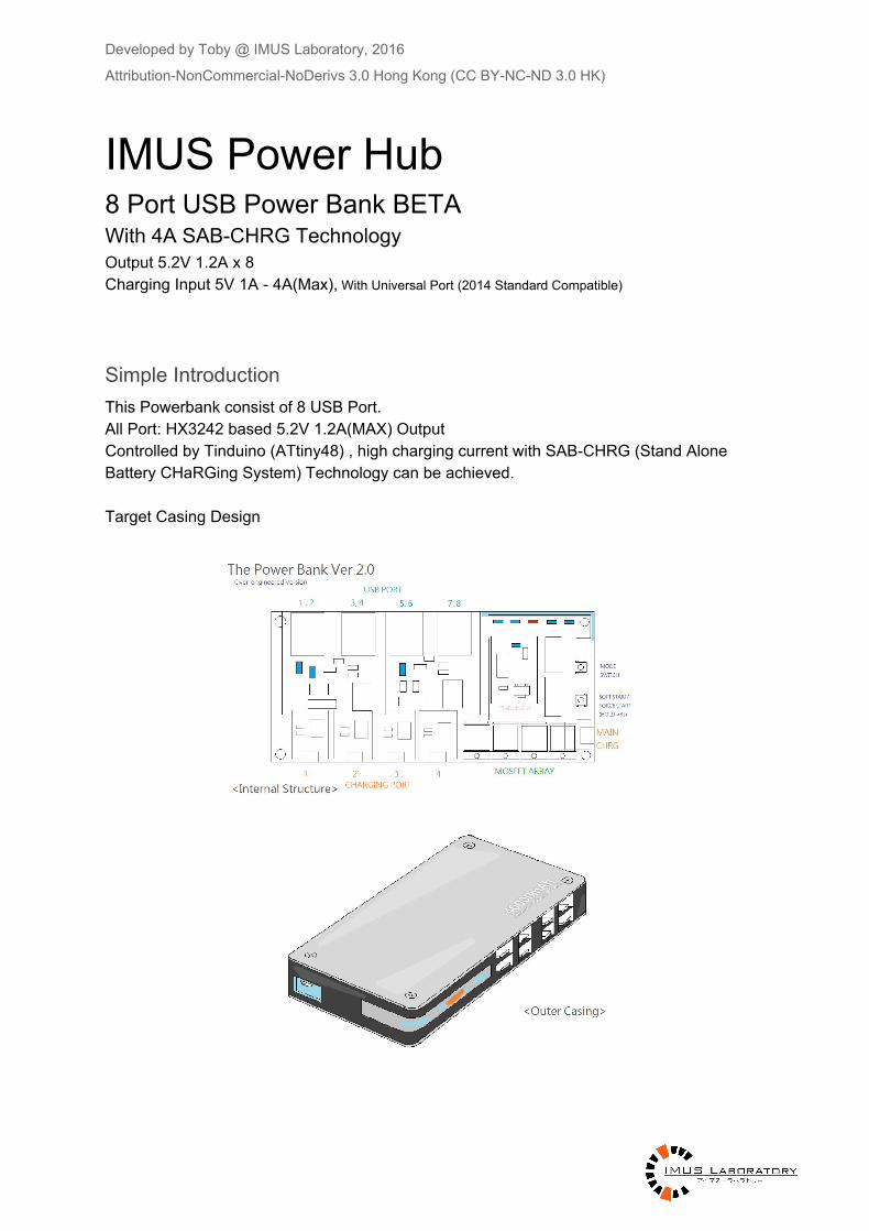
IMUS Power Hub 8 Port USB Power Bank BETA With 4A SAB-CHRG Technology Output 5.2V 1.2A x 8 Charging Input 5V 1A - 4A(Max), With Universal Port (2014 Standard Compatible)
Simple Introduction This Powerbank consist of 8 USB Port. All Port: HX3242 based 5.2V 1.2A(MAX) Output Controlled by Tinduino (ATtiny48) , high charging current with SAB-CHRG (Stand Alone Battery CHaRGing System) Technology can be achieved. Target Casing Design
Developed by Toby @ IMUS Laboratory, 2016
Attribution-NonCommercial-NoDerivs 3.0 Hong Kong (CC BY-NC-ND 3.0 HK)
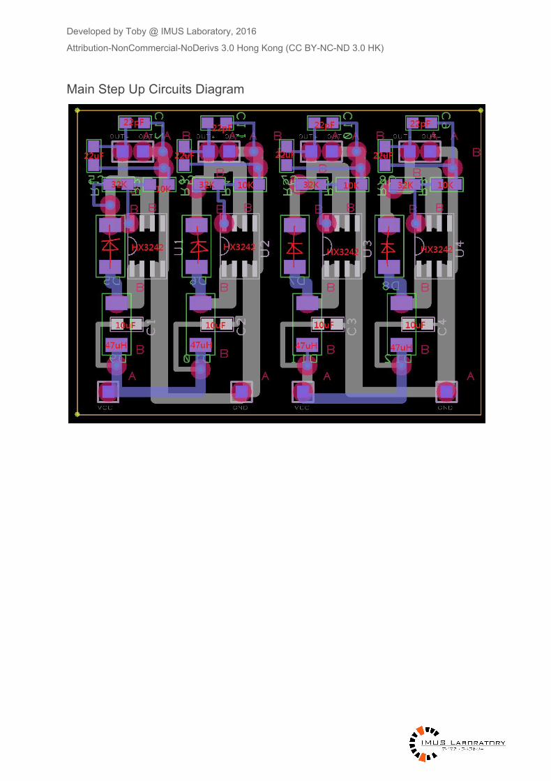
Main Step Up Circuits Diagram
Developed by Toby @ IMUS Laboratory, 2016
Attribution-NonCommercial-NoDerivs 3.0 Hong Kong (CC BY-NC-ND 3.0 HK)
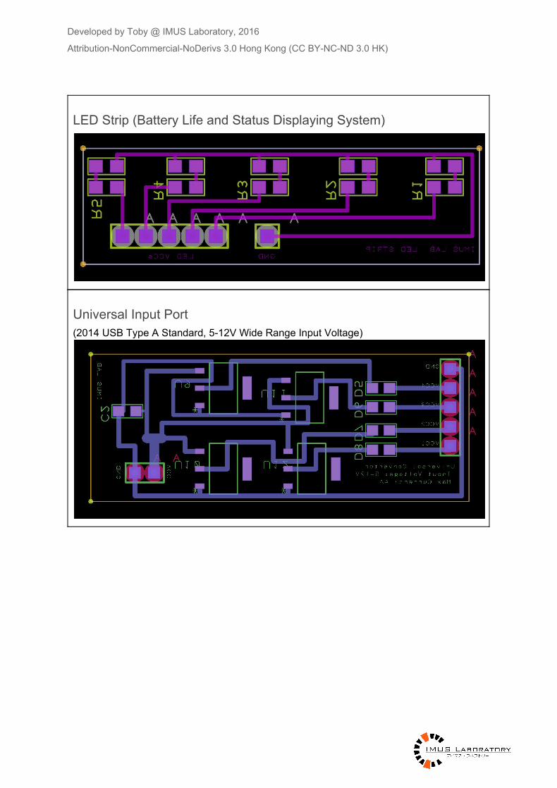
LED Strip (Battery Life and Status Displaying System)
Universal Input Port (2014 USB Type A Standard, 5-12V Wide Range Input Voltage)
Developed by Toby @ IMUS Laboratory, 2016
Attribution-NonCommercial-NoDerivs 3.0 Hong Kong (CC BY-NC-ND 3.0 HK)
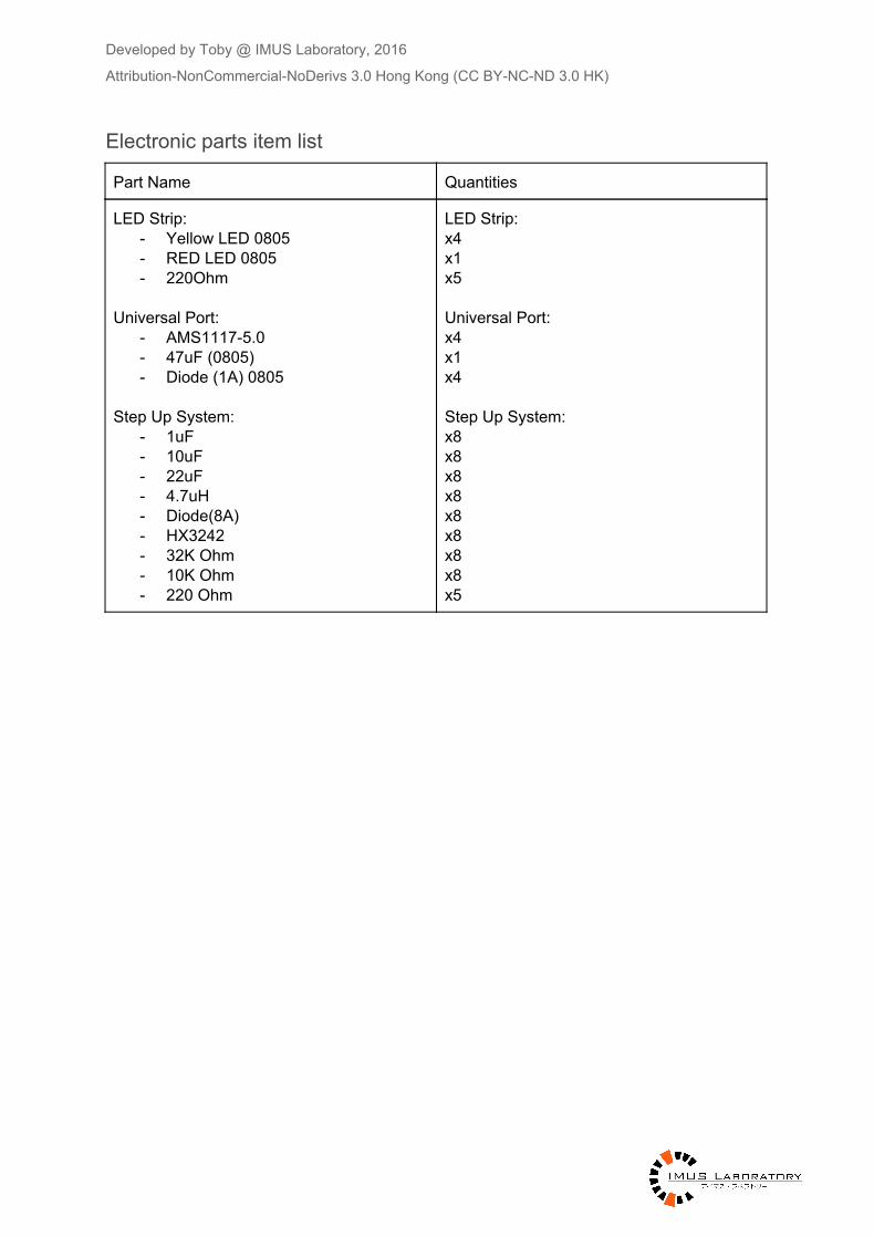
Electronic parts item list
Part Name Quantities
LED Strip: - Yellow LED 0805 - RED LED 0805 - 220Ohm
Attribution-NonCommercial-NoDerivs 3.0 Hong Kong (CC BY-NC-ND 3.0 HK)
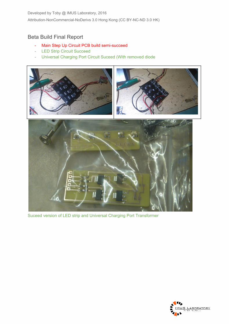
Beta Build Final Report - Main Step Up Circuit PCB build semi-succeed - LED Strip Circuit Succeed - Universal Charging Port Circuit Suceed (With removed diode
Suceed version of LED strip and Universal Charging Port Transformer
Developed by Toby @ IMUS Laboratory, 2016
Attribution-NonCommercial-NoDerivs 3.0 Hong Kong (CC BY-NC-ND 3.0 HK)
Failure Log on Main Step Up Circuit PCB 1. When there is no load, with 32K (3302) and 10K (106) have an output of 5.18V 2. When there is load (Sony Xperia, 15000mAh Thin Powerbank Rebuilt 1, 21000mAh
Camping Power Bank), the voltage dropped to 4.7V with 0.5A 3. Modifying the resistor to 8.2K and 32K, which have an output voltage of 5.8V. 5.4V
and 0.86A while with load. **Sony Xperia Cut off charging due to over voltage
4. Modifying the resistor to 8.0K (3.9K * 2) and 32K (28K reading on multimeter) gives 6.0V, charging load with 5.6V and 0.97A. **Sony Xperia cut off charging due to over voltage
5. Development of Beta Step Up PCB Terminated
Developed by Toby @ IMUS Laboratory, 2016
Attribution-NonCommercial-NoDerivs 3.0 Hong Kong (CC BY-NC-ND 3.0 HK)