DEVELOPMENT OF A HIGH POWER STABILIZED DIODE LASER SYSTEM by MATTHIAS FUCHS A THESIS Presented to the Department of Physics and the Graduate School of the University of Oregon in partial fulfillment of the requirements for the degree of Master of Science June 2006
Transcript
DEVELOPMENT OF A HIGH POWER STABILIZED DIODE LASER SYSTEM
by
MATTHIAS FUCHS
A THESIS
Presented to the Department of Physicsand the Graduate School of the University of Oregon
in partial fulfillment of the requirementsfor the degree ofMaster of Science
June 2006
ii
“DEVELOPMENT OF A HIGH POWER STABILIZED DIODE LASER SYSTEM,”
a thesis prepared by Matthias Fuchs in partial fulfillment of the requirements for the
Master of Science degree in the Department of Physics. This thesis has been approved
and accepted by:
Professor Daniel Steck, Chair of the Examining Committee
Date
Committee in charge: Professor Daniel Steck, ChairProfessor Michael RaymerProfessor Stehphen Gregory
Accepted by:
Vice Provost and Dean of the Graduate School
DEVELOPMENT OF A HIGH POWER STABILIZED DIODE LASER SYSTEM
Copyright June 2006
by
Matthias Fuchs
iv
An Abstract of the Thesis of
Matthias Fuchs for the degree of Master of Science
in the Department of Physics to be taken June 2006
Title: DEVELOPMENT OF A HIGH POWER STABILIZED DIODE
LASER SYSTEM
Approved:Professor Daniel Steck
This thesis describes the design and realization of a high power diode laser system.
The system consists of a single mode external cavity diode laser (ECDL) which is
injection locked into a free running laser diode. The beam of this low power master-
slave configuration is coupled into a high power tapered amplifier diode. The goal
of the laser system is to provide a dipole trap for ultra-cold Rubidium atoms. The
output power of the system is 1 W.
v
DEDICATION
This is for my parents and for Matthias Baar, who left us long before his time.
vi
ACKNOWLEDGEMENTS
Without all the help of my collegues and friends, I could never have successfully
finished the task that I’m describing in this thesis.
First of all I want to thank my adviser Dan Steck. He was always there when
I needed advice, whether it was on theoretical concepts, experimental procedures or
just a good idea to put drain pipe cleaner on food. He always took time to explain and
to discuss physics problems. He invented the long, long tradition of the weekly Friday
ice cream, which definetly contributed to the relaxed atmosphere in the lab. I also
want to thank my lab mates for helping me and providing a fun working environment.
Tao Li was a great help to me in explaining some optics setup procedures. It was
always fun and interesting to talk with him about Chinese culture and sports.
Libby Schoene added a female note to the lab and just by her presence made
being in the lab a nicer experience. I always enjoyed discussing both physics and
non-physics related subjects with her.
It was also a pleasure to bug Aaron Webster by any means possible. He is just the
man to have weird conversations with and to tell funny stories. Jeremy Thorn always
reminded me when it was “cookie time”. He helped me greatly in writing a program
that fetches data from the voltmeter. Otherwise, my measurements would have taken
about a Zillion years. Jeremy and Aaron were also responsible for introducing me to
some very instructive short movies about the Martians from Sesame Street.
vii
Finally, I cannot forget Peter Gaskell who was always very helpful when I had
problems with electronics or computers.
Overall, there is a very good working atmosphere in the Steck lab that made me
get up every morning and willingly go to work. I am very confident that this lab and
of course the people working in it have much potential and eventful, successful and
bright futures.
Without the people working in the machine shop I could also never have built
such a device. Kris, John and Jeff showed me how a lathe and a milling machine
work, and even managed to teach me how to machine precise parts. They were all a
big help when I needed suggestions on how to machine . . . basically anything.
I also want to thank Emelie. Without her, I probably would never have started
this project. I want to thank her for all her love and all the wonderful time that we
could spend together. She was there for me every day and helped me through the
dark days full of frustation, but she was also there to share my joy. The walks with
her often helped me to get my thoughts off of problems and to rejuvinate my mind
and eventually solve the problems with fresh ideas. She is constant source of joy. Her
endless will to bug me and her sense of humor infinitly brightened up my life.
Of course, I also want to thank my parents, my brother, and my friends back in
Germany. Although we were spatially very far separated, we were very close in spirit.
It is not an easy step to leave one’s home to live in a foreign country, but all my
friends and family supported me and helped me with my decision.
viii
And then I came to the US . . . and made more friends. They all helped me to
have a good time here and even made me stay longer than I originally planned. I can
definitely conclude that these two years in the US were among the best years of my
live.
ix
CURRICULUM VITA
NAME OF AUTHOR: Matthias Fuchs
PLACE OF BIRTH: Ellwangen, Germany
DATE OF BIRTH: August 6, 1980
GRADUATE AND UNDERGRADUATE SCHOOLS ATTENDED:
University of OregonUniversitat Stuttgart, Germany
DEGREES AWARDED:
Master of Science in Physics, 2006, University of OregonVordiplom in physics, 2003 Universitat Stuttgart
Figure PageI.1 Blue (left) and red detuned (right) Gaussian laser beam that repel and
attract atoms, respectively. . . . . . . . . . . . . . . . . . . . . . . . . . 3II.1 Gain curve of a laser with the modes of the resonator. . . . . . . . . . . 15II.2 p-n junction with an external potential U . . . . . . . . . . . . . . . . . . 18II.3 Cut through a p-i-n heterostructure energy diagram, size of electrons and
holes not to scale. . . . . . . . . . . . . . . . . . . . . . . . . . . . . . . . 20II.4 One dimensional energy diagram for electrons and holes. Ec is the energy
of the conduction band, Ev the energy of the valence band. An electroncombines with a hole and a photon of energy ~ω is emitted. . . . . . . . 21
II.5 Radiative transitions in semiconductors: a.) spontaneous emission, b.)stimulated emission and c.) stimulated absorption. . . . . . . . . . . . . 22
II.6 Energy diagram of a multi-quantum well surrounded by a confinementstructure. . . . . . . . . . . . . . . . . . . . . . . . . . . . . . . . . . . . 27
II.7 The peak emission wavelength of a diode laser. The dashed line representsthe change of the peak gain and the solid line the changes of the cavitylength and the refractive index. After [3]. . . . . . . . . . . . . . . . . . 29
II.8 Schematic drawing of a tapered amplifier. . . . . . . . . . . . . . . . . . 30II.9 Far-field intensity pattern of a tapered amplifier. . . . . . . . . . . . . . 34II.10 Picture of the tapered amplifier compared to a match. The golden colored
part is the c-mount of the diode. The real diode is the small blue dot ontop of the mount. It appears to be blue in this picture but it is black inreality. . . . . . . . . . . . . . . . . . . . . . . . . . . . . . . . . . . . . . 35
III.1 Picture of the optical setup. . . . . . . . . . . . . . . . . . . . . . . . . . 36III.2 Picture of the master laser. The path of the laser beam is indicated by
the red line. . . . . . . . . . . . . . . . . . . . . . . . . . . . . . . . . . . 37III.3 Picture of the Slave Laser. . . . . . . . . . . . . . . . . . . . . . . . . . . 41III.4 Schematic of the optical setup. . . . . . . . . . . . . . . . . . . . . . . . 42III.5 Tapered amplifier with the out-coupling optics to compensate for the astig-
matism. . . . . . . . . . . . . . . . . . . . . . . . . . . . . . . . . . . . . 48III.6 Sideview of the tapered amplifier housing. . . . . . . . . . . . . . . . . . 51III.7 Picture of the tapered amplifier housing. . . . . . . . . . . . . . . . . . . 53III.8 Schematic of the protection circuit. The diodes prevent the TA from
forward and backward transients, the ferrit bead and the capacitors forma low-pass filter. The ferrite beads (1) are Panasonic EXC-ELSA 35. . . 54
III.9 Schematic drawing of the tapered amplifier housing. . . . . . . . . . . . 55
xiii
IV.1 Horizontal beam profile of the amplified spontaneous emission at a currentof ITA = 0.75A, after the collimation and the cylindrical lens. . . . . . . 57
IV.2 Horizontal beam profile of the amplified spontaneous emission at a currentof ITA = 0.75A, after the collimation and the cylindrical lens. . . . . . . 58
IV.3 Low resolution ASE spectrum at ITA = 1.5A and 17.5 C. . . . . . . . . 59IV.4 Power of the input laser versus the amplified power for two amplifier cur-
rents: 1600 mA and 2000 mA. . . . . . . . . . . . . . . . . . . . . . . . . 60IV.5 Temperature dependence of the output power versus the driving current. 60IV.6 Output power versus current for two different seed powers of 8 mW and
13 mW. . . . . . . . . . . . . . . . . . . . . . . . . . . . . . . . . . . . . 61IV.7 Spectrum of the TA for a output power of 0.5 W. The solid curve is
optimized for the most absolute power, the dashed curve for the mostpower at 780 nm. The inlet shows the difference between both graphs.Note: the inlet has a linear y-axis. . . . . . . . . . . . . . . . . . . . . . 62
IV.8 Horizontal profile for a seeding laser power of Pseed = 8 mW and anamplifier power of PTA = 100 mW. . . . . . . . . . . . . . . . . . . . . . 64
IV.9 Vertical profile for a seeding laser power of Pseed = 8 mW and an amplifierpower of PTA = 100 mW. . . . . . . . . . . . . . . . . . . . . . . . . . . 65
IV.10Horizontal profile of the TA for the same input power of 8 mW and anoutput power of the tapered amplifer of 100 mW and 400 mW. . . . . . 65
IV.11Vertical profile of the TA for the same input power of 8 mW and an outputpower of the tapered amplifer of 100 mW and 400 mW. . . . . . . . . . 66
IV.12Horizontal beam profile for different input powers at the same outputpower of 100 mW. . . . . . . . . . . . . . . . . . . . . . . . . . . . . . . 67
IV.13Vertical beam profile for different input powers at the same output powerof 100 mW. . . . . . . . . . . . . . . . . . . . . . . . . . . . . . . . . . . 67
V.1 Picture of the tapered amplifier, emitting to the left, with the two colli-mation lenses. . . . . . . . . . . . . . . . . . . . . . . . . . . . . . . . . . 68
A.1 Drawing of the large copper block (A). . . . . . . . . . . . . . . . . . . . 70A.2 Drawing of the baseplate with water-cooling ability. . . . . . . . . . . . . 71
1
CHAPTER I
INTRODUCTION
In recent years, semiconductor diode lasers have shown improved reliability, power,
and wavelength coverage. With the ability to provide more power, diode lasers can
now compete with heavy and bulky gas and other solid-state lasers. They have become
increasingly common in industrial applications, since they are compact, easy to cool,
and have a power efficiency upwards of 50%. Another advantage of diode lasers is
that they can have a very high spatial beam quality, and their frequency can be very
easily and rapidly tuned by changing the injection current. Furthermore, with the
development of the semiconductor industry, they have also become less expensive.
Concerning the work in science, diode lasers have become one of the workhorses
for atomic physics. In order to confine ultra-cold rubidium atoms in a dipole trap,
powerful lasers with a wavelength in the vicinity of 780 nm are often used. Atoms are
scattered out of a dipole trap at a rate of Γsc ∼ I/∆2 with I being the intensity of
the laser beam and ∆ the detuning of the beam frequency from the atomic transition.
Therefore a far detuning is needed. However, since the potential of the trap has a
dependence of U ∼ I/∆, a high intensity beam is also necessary.
2
I.1. Dipole Trap
First, a brief overview of the dipole trap is given. For a more in-depth description,
refer to [1].
The dipole trap confines neutral atoms using the interaction of light with an atom.
Light is nothing more than an electromagnetic field that exerts a force on an electric
dipole moment. Since rubidium is a neutral atom, it possesses in the ground state
no permanent electric dipole moment. But the field of a laser induces a shift on the
energy states of an atom. This shift, known as the AC Stark shift or light shift, is a
change of potential energy of the atom. Therefore, if the potential is lowered by the
interaction with the light and the electromagnetic field of the laser is inhomogeneous
(has a gradient), the atom moves to the place with the lowest potential, which is the
spot with the highest field. Since the induced shift is not static but oscillatory, the
frequency of the laser light also has to be taken into account. If the light is below
the atomic resonance (red detuned), the energy of the ground state and therefore
the potential is lowered, resulting in an attractive force towards the highest intensity
of the field. On the other hand, if the light frequency is higher than the resonance
frequency (blue detuned), the ground state is raised, which means that the atom is
repelled by high intensities. This behavior can be understood by using the classical
Lorentz model of an atom. In this model the atom consists of a very heavy core
(compared to the electron) and an electron which is bound to the core via a spring
3
FIGURE I.1: Blue (left) and red detuned (right) Gaussian laser beam that repel andattract atoms, respectively.
representing the electromagnetic force. If this system is now driven by an external
oscillator (the optical field) with a frequency below the resonance frequency, the
system can “keep up” and stays in phase with the light field thus drawing the atom
into the region where the oscillator is the strongest. If the oscillator frequency exceeds
the resonance, the system can no longer follow and becomes out of phase, so that the
dipole moment opposes the light field and the atom is repelled by high intensities.
I.2. Quantum-Mechanical Description
A quantum-mechanical formulation is now presented to give an overview of the
mathematical description of the dipole trap.
The so-called “dressed-atom picture” describes the coupling of a two-level atom
4
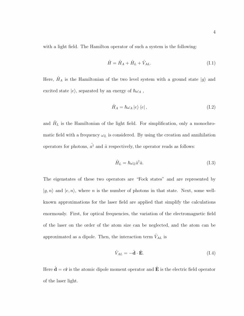
with a light field. The Hamilton operator of such a system is the following:
H = HA + HL + VAL. (I.1)
Here, HA is the Hamiltonian of the two level system with a ground state |g〉 and
excited state |e〉, separated by an energy of ~ωA ,
HA = ~ωA |e〉 〈e| , (I.2)
and HL is the Hamiltonian of the light field. For simplification, only a monochro-
matic field with a frequency ωL is considered. By using the creation and annihilation
operators for photons, a† and a respectively, the operator reads as follows:
HL = ~ωLa†a. (I.3)
The eigenstates of these two operators are “Fock states” and are represented by
|g, n〉 and |e, n〉, where n is the number of photons in that state. Next, some well-
known approximations for the laser field are applied that simplify the calculations
enormously. First, for optical frequencies, the variation of the electromagnetic field
of the laser on the order of the atom size can be neglected, and the atom can be
approximated as a dipole. Then, the interaction term VAL is
VAL = −d · E. (I.4)
Here d = er is the atomic dipole moment operator and E is the electric field operator
of the laser light.
5
The second approximation, known as the rotating wave approximation (RWA),
assumes |ωL − ωA| ωL + ωA and neglects the fast oscillating term (see [2]). For a
plane wave with an amplitude E0, the interaction term at a certain spatial position
(choose z = 0) becomes
VAL =~Ω
2(aeiωLt |e〉 〈g| + a†e−iωLt |e〉 〈g|), (I.5)
where Ω := −eE0 〈e| r |g〉 is the Rabi frequency. A transformation to a rotating frame
gets rid of the phase factors and the Hamiltonian becomes, using ∆L = ωL − ωA,
H = ~
−∆LΩ2
Ω2
0
. (I.6)
The eigenvalues of this Hamiltonian are:
Ee,g = −~∆L
2±
~
2
√
∆L2 + Ω2 (I.7)
In the limit of far detuning, |∆L| Ω, the energy shift can be expanded to first order
in Ω/∆L, yielding:
∆Eg =~Ω2
4∆L(I.8)
∆Ee = −~Ω2
4∆L. (I.9)
This is the Stark shift that induces the dipole moment, drawing the ground state atom
into high intensities for red detuning (∆L < 0) and repelling it from high intensities
for blue detuning (∆L > 0).
6
If an electrical field in the z direction is considered, the force acting on an atom is
F = −
⟨
∂VAL
∂z
⟩
, (I.10)
since this is the relevant term of the Hamiltonian that describes the interaction. The
result of this equation is [1]
F =~s
1 + s
(
−∆Lqr +1
2γqi
)
(I.11)
where s = I/[Is(1 + (2∆L/γ))] is the saturation parameter, Is = πhcγ/(3λ3) is the
saturation intensity, γ is the decay rate of the spontaneous emission and qr + iqi is
the logarithmic derivative of the complex function Ω. It is defined as ddz
ln[Ω(z)] =
(qr + iqi). For a travelling electro-magnetic wave, E = E0(ei(kz−wt) + cc.), the position
dependence is only in the phase and therefore qr = 0 and qi = k. For a standing
wave, E = E0 cos(kz)(e−iwt + cc.), qr = −k tan(kz) and qi = 0.
It can be seen that there are essentially two different forces acting on the atom.
The first is the spontaneous scattering force, which acts in the direction of laser
propagation
Fsp =~kγ
2Is
I
1 + I/Is + (2∆L/γ)2. (I.12)
It is related to the scattering rate Γsc in the following way:
Fsp = ~k · Γsc. (I.13)
The other force is the optical dipole force, which acts in the direction of the laser
7
intensity gradient,
Fdip =2~k sin 2kz
Is
I∆L
1 + 4I/Is cos2 kz + (2∆L/γ)2. (I.14)
By taking a closer look at Eqs. (I.12) and (I.14), it can be seen why the laser for
a dipole trap should be very powerful: The further the detuning ∆L of the laser,
the smaller the scattering rate, because it is proportional to I/∆2L. Since the dipole
potential is just proportional to I/∆L, a deep dipole trap can still be achieved by
using high laser intensities.
8
CHAPTER II
THEORY OF THE LASER
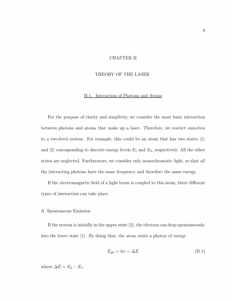
II.1. Interaction of Photons and Atoms
For the purpose of clarity and simplicity, we consider the most basic interaction
between photons and atoms that make up a laser. Therefore, we restrict ourselves
to a two-level system. For example, this could be an atom that has two states |1〉
and |2〉 corresponding to discrete energy levels E1 and E2, respectively. All the other
states are neglected. Furthermore, we consider only monochromatic light, so that all
the interacting photons have the same frequency and therefore the same energy.
If the electromagnetic field of a light beam is coupled to this atom, three different
types of interaction can take place.
A. Spontaneous Emission
If the system is initially in the upper state |2〉, the electron can drop spontaneously
into the lower state |1〉. By doing that, the atom emits a photon of energy
Eph = hν = ∆E (II.1)
where ∆E = E2 − E1.
9
This emission is random in direction, phase, and time, with the result that the
emitted light is incoherent.
The transition rate of this process is:
(
dn2
dt
)
spont. em.
= −γn2, (II.2)
where n2 is the population density of the state |2〉, γ is a the decay rate and the minus
sign comes from the fact that n2 is decreasing.
B. Absorption
Absorption occurs if a photon with resonance energy ∆E interacts with a system
that is in the state |1〉. The energy of the photon is absorbed with a certain probability,
and the system is raised into the upper state.
Since absorption depends on the light field as well as the population density n1 of
state |1〉, one can write the transition rate as:
(
dn1
dt
)
stim. abs.
= −B12u(ν)n1, (II.3)
with
u(ν) =8πhn3ν3
c3
1
exp( hνkBT
− 1)(II.4)
being the spectral energy density written in terms of Planck’s black-body radiation
formula of the stimulating photon field, B12 being the proportionality constant, and
the minus sign again indicating the decreasing of n1.
10
C. Stimulated Emission
The final interaction is the inverse process of absorption. It is again an emission,
but this time it is stimulated, meaning that the system is in the upper state when
a photon with the resonance frequency interacts with it. The photon stimulates the
system to drop into the lower state and emit another photon in the same mode as
the interacting photon. This means that the emitted photon has exactly the same
frequency, phase, direction of propagation, and polarization as the stimulating photon.
This process can be used to amplify an optical beam because it is a coherent radiation.
Light sources that produce light in this way are called LASERs (Light Amplification
by Stimulated Emission of Radiation). Many atoms in state |2〉 are needed to get a
reasonable amplification of the initial interacting light field. An ensemble of atoms
having a greater population density in the upper state than the lower state is called
“population inversion”.
Again, the transition rate depends on the spectral energy density u(ν) and the
population density n2,(
dn2
dt
)
stim. em.
= −B21u(ν)n2, (II.5)
with B21 being a proportionality constant.
II.2. Rate Equation
To describe the whole two-level system now, we must combine the three processes.
11
To this end, we follow the simple argument of Einstein who considered an ensemble of
atoms in thermal equilibrium in the presence of a light field of spectral energy density
u(ν).
Transitions from state |2〉 to state |1〉 comprise both spontaneous and stimulated
emission, so the total transition rate r21 is
r21 = γn2 + B21u(ν)n2 (II.6)
where γ and B21 are the Einstein coefficients of spontaneous and stimulated emission,
respectively.
The transition rate from the lower to the upper state is only comprised of absorp-
tion,
r12 = B12u(ν)n1 (II.7)
with B12 being the Einstein coefficient for stimulated absorption.
In thermal equilibrium both rates are equal, so that
γn2 + B21u(ν)n2 = B12u(ν)n1. (II.8)
Eq. (II.8) is known as the rate equation of a two level system. We will come back to
this equation later, when we will discuss it in the context of the diode laser.
II.3. Elements of a Laser
The laser is essentially an optical oscillator. Parts of the output of this optical
12
resonator are fed back with the correct phase into the input. In order to achieve this,
a laser usually consists of three elements.
The active medium is a medium with population inversion such that a light field
propagating through it will be amplified by stimulated emission.
The pump delivers energy to the active medium so that there can be a population
inversion. The pump can consist of a flash lamp, gas discharge or another laser. In
the case of a diode laser, the pump is very convenient, as it is just an electrical current
that places charge carriers in the active medium so that population inversion can be
achieved.
Finally, an optical resonator is required. This is usually accomplished with a
Fabry-Perot-Interferometer (FPI). Due to the boundary conditions of a FPI, only
certain modes that form a standing wave inside the cavity can be excited. The
condition for a standing wave is:
L = mλ0
2neff(II.9)
with λ0 being the vacuum wavelength, neff the effective refractive index of the cavity
and m = 1, 2, 3, . . . .
The resonator stores some of the radiation emitted by the active medium in a few
modes so that the number of photons in these modes is n 1. This increases the
probability of stimulated versus spontaneous emission. The resonator is also recycling
13
modes back into the active medium so that another cycle of stimulated emission is
started by photons in the same mode and the laser light stays unaltered. The result
is a light oscillator rather than a light amplifier.
For a semiconductor laser, the active layer also acts as the cavity. Using a coating
on the front and back facets, the required reflectivity can be achieved. Depending on
the index of refraction and the thickness of the layer, an antireflection coating can
be applied. The standard material for this is Al2O3, which also has the advantage
of being able to passivate and protect the extremely sensitive facets. By alternating
layers of Al2O3 and Si, a so-called Bragg reflector with a high reflection coefficient can
be created. For high power diode lasers, the back facet is usually highly reflective,
whereas the front facet is antireflection coated, so that the photon density inside
the cavity is reduced. This effectively eliminates destructive interference from back
reflection of the front facet and results in an increased output power.
II.4. The Principle of a Laser
Usually the active medium is surrounded by the resonator. One of the resonator’s
windows is partially transmitting so that the laser light can be extracted through it,
but there is still enough reflection to maintain an oscillating wave in the resonator.
Another crucial condition, of course, is that the pump provides enough power to
compensate for the emitted laser beam and other losses.
If the active medium is in a state of population inversion, and the interacting
14
optical field is strong enough to make stimulated emission the dominant process,
then an incoming photon of the right frequency will produce another photon emitted
in exactly the same mode. Now, both of those photons can stimulate two other atoms
to emit photons in the same mode, etc. This means that one incoming photon can
produce an avalanche of photons in the same mode, and therefore the intensity of the
electromagnetic wave traveling in the z-direction grows exponentially, neglecting gain
saturation effects:
I(ν, z) = I(ν, 0)eα(ν)z. (II.10)
When α(ν) < 0, this is known as Beer’s law of absorption.
Since the resonator only sustains frequencies that correspond to wavelengths form-
ing a standing wave in the resonator, only a few modes of the continuous gain spec-
trum are selected (Fig. II.1). Furthermore, only the modes where the resonator
spectral line intersects the gain curve above threshold are amplified.
II.5. The Diode Laser
Semiconductors
Due to the overlap of the atomic orbitals in a semiconductor, the electrons aren’t
located in discrete levels as in a single atom. Instead they form a continuous “band
structure.” The band structure consists of a conduction and a valence band, separated
by an energy gap Eg, which is typically 0.5 - 2.5 eV. The conduction band is filled with
15
wavelength
gain
threshold
FIGURE II.1: Gain curve of a laser with the modes of the resonator.
electrons and in an undoped material there are as many holes in the valence band
as electrons in the conduction band. Holes are “missing” electrons in the valence
band that can also move and therefore conduct current. Due to the continuous
band structure, the electrons in the conduction band and the holes in the valence
band can move nearly freely and can thus be approximately described as an electron
gas. Therefore, the electrons in thermal equilibrium in a semiconductor are Fermi-
distributed,
f(E, T ) =1
exp(E−EF
kBT) + 1
, (II.11)
where EF is the Fermi energy. For T = 0 K, f becomes a step function with the value
f = 1 for energies below the Fermi energy and f = 0 above EF , which means that all
electrons are in the valence band.
16
Doped Semiconductors
The properties of a semiconductor (where the atoms forming a semiconductor are
in group IV) can easily be changed by doping it with atoms of groups III and V. If a
semiconductor is doped with atoms of group V (P, AS,...), just 4 of the outer electrons
of the atom take part in the chemical bonding, and one electron is very weakly bonded
to the atom. The result is that the 5th electron has a very low ionization energy (≈
0.1 eV or smaller). These electrons sit on an energy level that is higher than the
energy of the conduction band and very close to the valence band. Therefore, the
Fermi energy of the so-called n-doped semiconductor rises to this level.
For p-doping, one puts some atoms from group III (B, In,...), having just 3 outer
electrons in the semiconductor, and instead of electrons with energies close to the
conduction band, one gets holes with energies close to the valence band and a lower
Fermi energy.
p-n Junction
If p- and n-doped semiconductors are brought into metallurgical contact, electrons
and holes will diffuse from areas of high concentration to areas with low concentration
due to thermal motion. Electrons go from the n to the p part, where they recombine
with the abundant holes, leaving behind positively charged atoms. On the other hand,
holes diffuse in the opposite direction and recombine with electrons leaving behind
negatively charged atoms. Therefore, the area in the middle of the p-n junction,
called the depletion layer, loses all its mobile charge carriers, and what remains are
17
just the fixed positive ions on the n side and the negative ions on the p side. As a
result, an electric field (and therefore a potential) is built up between the two sides.
In terms of the energy diagram, the p part has more negative charge, which raises
the Fermi energy and vice versa for the n part. Since both parts are in contact, the
Fermi levels align, producing a bend in the band structure(Fig. II.2).
If in addition an external potential is applied, the potential difference between
the two layers can be changed. We will just discuss the forward-biased case, where
a positive potential U is applied to the p side. In this case, electrons are sucked
away from the p-doped part into the source causing the Fermi level (and therefore
the band energy) to be lowered. The converse is true for the n-part, where electrons
are injected. As a result, the potential barrier decreases, and it is easier for charge
carriers to cross over.
The current depends on the voltage through the relationship [7]:
j = j0(eeU/KBT − 1), (II.12)
where j0 is the drift current.
This formula shows why this is also called a diode: for U > 0, we get an exponen-
tially increasing current, that saturates for higher voltages.
Due to the external potential, the semiconductor is no longer in an equilibrium
state. The Fermi energies of the valence and conduction bands, EFc and EFv, are
becoming misaligned. As a result of this misalignment, there are two different Fermi
levels in the depletion layer, which represent a state of equilibrium. To describe this
FIGURE II.4: One dimensional energy diagram for electrons and holes. Ec is theenergy of the conduction band, Ev the energy of the valence band. An electroncombines with a hole and a photon of energy ~ω is emitted.
states, it is necessary that the maximum and the minimum of the valence and the
conduction bands have the same wavenumber k. Such a structure is known as a direct
semiconductor.
Therefore, to describe the transitions of semiconductors for a fixed photon energy
~ω, it is correct to consider the two-level system with discrete energy levels as men-
tioned above. However, in a semiconductor, the transition rate depends not only on
the available charge carrier in one of the states but also on the missing charge carrier
in the other band. Hence, the transition rate for spontaneous emission has to be
FIGURE II.6: Energy diagram of a multi-quantum well surrounded by a confinementstructure.
direction and perpendicular to the growth direction of the semiconductor, and TM
(transverse magnetic) which is parallel to the growth direction.
To describe the polarization of a diode laser, we must consider a more detailed
model of the band structure, in which the valence band consists of three sub-bands.
The sub-bands are a result of the 4p state of the GaAs “molecule” in which the spin-
orbit coupling leads to the total angular momentum j = 3/2 and j = 1/2. Here,
we only consider the j = 3/2 states and refer to mj = 3/2 and mj = 1/2 as “heavy
holes” and “light holes”, respectively.
These two sub-bands are usually degenerate at the momentum state k = 0. But
for example in a strained quantum well device, as described above, the bands can
split up.
28
To find the probability for a radiative transition, the dipole moment matrix ele-
ment is calculated by
µif = 〈i| d |f〉 , (II.28)
where |i〉 is the initial (electron) state, |f〉 is the final (hole) state and d is the dipole
operator from Eq. (I.4). This becomes 〈i| ez |f〉 for TM polarization and 〈i| ex |f〉 for
TE polarization.
Plugging in the correct wave-functions and using the symmetry dependence of the
electronic, the heavy and the light hole states, we find that the TM dipole matrix
element only couples the electron to the light hole state [9]. Whereas the TE dipole
matrix element couples the electron to both the heavy and light hole states, depending
on the carrier momentum. However, for k ≈ 0 it couples mostly to the light holes.
So, the radiation may have a different polarization, depending on the strain of the
quantum well and therefore on the lasing frequency.
II.8. Current, Temperature and Frequency Dependence
The wavelength of the emitted laser light of a diode depends primarily on the
energy of the band gap Eg, but by manipulating the injection current and the tem-
perature of the diode, it can be changed within a bandwidth of up to 30 nm [19].
The wavelength of the light responds to temperature changes because the optical
path length of the cavity, the refractive index and the gain curve are temperature
dependent. However, the sensitivity to each of these effects is quite different. For
29
-20 -10 0 10 20 30 40 50 60 70
970
980
990
10000.2 nm/K
0.3 nm/K
Temperature (°C)
Wav
elen
gth
(nm
)
FIGURE II.7: The peak emission wavelength of a diode laser. The dashed linerepresents the change of the peak gain and the solid line the changes of the cavitylength and the refractive index. After [3].
an AlGaAs diode, the optical length of the cavity and the refractive index have a
combined effect on the wavelength of about 0.06-0.2 nm/K. The gain curve changes
by about +0.33 nm/K, due to the variation of the gap between the energy bands. This
makes the overall temperature-wavelength curve appear as a sloped staircase (Fig.
II.7). The discrete steps in the staircase are due to hops between different modes
of the resonator. The slope of the individual stairs originates from the continuously
changing cavity length, which changes the resonance frequency.
Changing the injection current has two effects on the laser diode. First, it changes
the temperature and second, it changes the carrier density in the active zone, which
in turn changes the refractive index. Since a higher current produces Joule heating,
this effect looks very much the same as the temperature-wavelength dependence. The
30
p-InGaAs
n-InGaAs
GaAs-substrate
GaAsP - Quantum well
active region
tapered gain region
p - contactantireflection
coatedantireflection
coated
x
y
FIGURE II.8: Schematic drawing of a tapered amplifier.
change of the refractive index is small and only matters for high-frequency modulation
of the current.
II.9. The Tapered Amplifier
In order to maintain a single spatial mode, the transverse dimensions of the wave-
guide of a conventional semiconductor laser have to be on the order of the wavelength.
This confinement limits the output power of the laser due to heating of the bulk
and the facets. On the other hand, devices with a much broader gain region, like
broad area lasers, can produce higher intensity light, but they oscillate in very high
order lateral modes. The tapered amplifier combines these two essential features. As
depicted in Fig. (V.1), it consists of two parts: a straight index-guided waveguide
section and a gain-guided tapered section. The beam of the master oscillator is
31
coupled into the small end and then expands laterally because of diffraction, filling
the tapered gain region of the device. The straight part is used as a modal filter
to excite only the fundamental transverse mode and it has the advantage that only
a low input power is needed to achieve sufficiently large energy densities. By just
using a small-sized straight guide, the laser could not reach such high powers. Those
high power densities would give rise to the nonlinear optical Kerr effect which would
change the refractive index depending on the light intensity. This would lead to a
self-focusing effect and destroy the material. The tapered section therefore makes
sure that the energy density is kept below the critical value, while still achieving high
output powers that maintain the single mode behavior. However, the beam shape is
still altered through undesired power-dependent changes of the charge carriers and
temperature induced refractive-index perturbations that decrease the beam quality
and brightness. A typical length of the tapered region is about 2-3 mm and the input
aperture of 5-10 µm expands to about 200 µm. Electrical contact is established by
metallizing the top and bottom layers. The front and back facets are anti reflection
coated (Rf ≈ 0.1%) to assure a low energy density in the cavity, a suppression the
laser’s eigenmodes and minimal reflection. Such reflection can lead to destructive
interference and irregular intensity fluctuations, which in turn can result in multi-
mode behavior.
To understand the tapered amplifier, a simple and descriptive model is presented.
The input beam is focused tightly enough into the input aperture, so that after the
32
waveguide, it diffracts with the angle of the taper and fills out the whole gain medium.
If the gain medium is long enough, the spontaneous emission is small compared to the
stimulated emission, initiated by the input beam. Since the gain region is pumped
by a spatially homogeneous current density, the gain along the propagation axis is
uniform. But since the gain varies with the inverse of the local optical power density,
it is not laterally uniform. This means that an incoming Gaussian beam experiences
a lower gain at the center than in the outer regions because it saturates first for
larger intensities. As a result, it approaches a more and more flat-hat distribution,
which is uniform over a certain area and zero outside. Due to pertubations from this
model such as carrier diffusion, non linear and thermal effects and non uniform carrier
injection, the intensity pattern will deviate from this model, but nevertheless, a good
understanding of the amplifier can be extracted from it.
Since the beam expands from the small waveguide and diffracts at the tapered
angle, the amplitude and phase will be uniform along the curved wavefronts extending
from the aperture, but not along the flat surface of the emitting facet. However, a
uniform phase along the surface (and therefore a diffraction-limited beam) can be
obtained to a high degree of approximation. After the beam is emitted from the
front facet, it obeys Snell’s law. For small angles, the diffraction angle is the angle
of the taper times the lateral modal index nl. For a taper angle of ≈ 6 this yields
a diffraction angle of about 20. Since the wavefronts are not perfectly planar but
curved, the beam emitted by the wide aperture seems to emanate from a point inside
33
the diode. This virtual source point is a distance of approximately L/nl behind the
output facet, where L is the length of the amplifier. On the other hand, the beam
profile perpendicular to the wide side of the facet is diffracted at the facet with an
angle of 30-40 . Thus, it can be seen that the beam is astigmatic, which means that
it has different focal points for the two perpendicular directions after it propagates
through a spherical lens.
To get the far-field distribution in the horizontal plane, an ideal cylindrical lens
is placed a focal length faway from the aperture. Therefore, the Fresnel integral for
the propagated field has to be solved:
E(x, y, z) ∝
+∞∫∫
−∞
E0(x′, y′)e−iΦ(x′,y′)e
−ik0
2z(x′2+y′2)ei(kxx′+kyy′)dx′dy′. (II.29)
here, k0 = ω0/c is the wavenumber, ω0 is the frequency of the light, E0(x′, y′) is
the electrical field at the aperture, Φ(x′, y′) is the phase induced by the cylindrical
lens and kx = k0xf
. The second term in the integral, the induced phase by the lens,
is chosen such that the product with the quadratic phase-curvature term, the third
term in the integral, is equal to unity. This means that the far-field intensity pattern
is the squared Fourier-transform of the field distribution at the output fact.
To calculate the far-field of the TA, the flat-hat distribution with a uniform phase
at the output facet is considered. Considering that the thin lens, by definition, just
affects the phase of the beam, one can calculate the the lateral power density as a
function of angle P (φ). This is nothing other than the squared Fourier transform of
34
0
0.1
0.2
0.3
0.4
0.5
0.6
0.7
0.8
0.9
1
−2 −1.5 −1 −0.5 0 0.5 1 1.5 2
Rel
ativ
eIn
tensi
ty
Angle φ (deg)
FIGURE II.9: Far-field intensity pattern of a tapered amplifier.
the flat-hat distribution [5]
P (φ) ∝sin2[Dπ sin(φ)/λ]
(πD sin(φ)/λ)2, (II.30)
with D being the width of the output facet, φ the far-field angle and λ the emit-
ted wavelength. From Eq. (II.30), we can see that approximatly 90% of the beam
intensity lies inside the central lobe of the far field pattern (Fig. II.9.)
The field at the output facet is in reality not flat-hat distributed. Deviations
from the ideal distribution lead to far-field patterns where the size of the central lobe
doesn’t change much, but the fraction of energy inside the lobe does. Therefore, an
analysis of the near-field can show degradations of the amplifier. Some reasons for
degradations are [5]: non-uniformities in the electrical and optical properties of the
35
FIGURE II.10: Picture of the tapered amplifier compared to a match. The goldencolored part is the c-mount of the diode. The real diode is the small blue dot on topof the mount. It appears to be blue in this picture but it is black in reality.
material, strains introduced by fabrication and packaging and heat sinking, strains
at the edges of the tapered region where the metal layers are deposited, non-linear
self-focusing effects, spatial hole burning effects and spatial fluctuations in the seeding
beam.
The amplifier diode is mounted upside down on a c-mount (Fig. II.10), which acts
as a heat sink and an electrical contact. The n-side is contacted by wire bonding.
36
CHAPTER III
THE EXPERIMENTAL SETUP
FIGURE III.1: Picture of the optical setup.
III.1. The “Lasers” s
The optical setup consists of three lasers. The master laser is injection-locked to
the slave laser, which in turn is coupled into the tapered amplifier.
37
FIGURE III.2: Picture of the master laser. The path of the laser beam is indicatedby the red line.
III.2. Pseudo-External-Cavity Laser or the “Master”
A common way to achieve a narrow linewidth single mode operation with diode
lasers is to use the reflection of an external grating as an extended cavity. The master
laser is built in a Littrow configuration, which means that the beam of a laser diode
with a low-reflectance front facet is collimated with a lens and then reflected by a
grating. The zeroth order of the reflection is coupled out as a single-mode beam,
and the first order is coupled back into the diode. Therefore, the frequency of the
reflected light depends strongly on the angle of the grating. Since the reflection of
the grating is stronger than the reflection of the front facet, the grating provides
38
frequency-selective feedback and acts as one of the mirrors of the extended cavity.
The other mirror is the back facet of the diode. The frequency of the laser can be
tuned by changing the current and the angle of the grating via a piezo stack. The
output beam has a linewidth < 5 MHz. In order to achieve a mode-hop-free operation,
the angle, the current and the temperature need to be adjusted. However, because of
the competition between the free-running modes of the diode and the extended-cavity
modes, the tuning range is not truly mode-hop free, yet scanning over the rubidium
spectrum is possible without mode hops. However, by locking the laser frequency to
an atomic absorption line, long-term stability can be obtained.
Single-mode lasing properties are highly preferable, since other modes also draw
power in multi-mode lasing operation, which results in higher overall power consump-
tion and less power in the desired mode. Furthermore, multi-mode operation has more
noise due to the competition between the different modes.
The master laser used in the lab is design from Mark Raizen’s group at the Uni-
versity of Texas, modified for 780 nm. It uses a commercially available laser diode
from Sharp (GH0781JA2C), with an output of 120 mW at 140 mA. The front facet
of this diode is not anti reflection coated, which makes the laser a pseudo-external-
cavity laser. The frequency is locked via a lock-in amplifier to a cross over line of the
saturated-absorption rubidium spectrum. The frequency of the diode can be modu-
lated and swept by applying a voltage to the piezo and changing the current. See [16]
for more detailed information.
39
III.3. Frequency Stabilizing the Master Laser
The master laser is passively frequency stabilized. This laser and another already
stabilized laser are coupled into a comparing cavity that is able to scan the frequency
range by moving one of the mirrors. By measuring the slope of the transmission curve
dIT/dλ, it can be seen whether or not the lasers are locked.
The reference laser is locked to a cross over of the rubidium spectrum. To get a
very precise lock, the beam is coupled into a Doppler-free absorption setup. Here,
the laser is splitted into a strong pump and a weaker probe beam. Both beams prop-
agate through a rubidium vapor cell, but in opposite directions at slightly different
angles. Since the velocities of the rubidium atoms in the cell are Maxwell-Boltzmann
distributed, the cell shows a Doppler-broadened absorption spectrum. Now, if the fre-
quency of the laser coincides with a transition frequency of the rubidium, the pump
laser excites atoms and their population is transfered to the upper state. Therefore,
the probe beam doesn’t get absorbed and if the frequency of the laser is scanned, the
“Lamb dip” can be seen in the absorption spectrum. This only happens at atomic
resonances because for other frequencies, the pump and the probe beam excite dif-
ferent Doppler-shifted atoms moving in opposite directions. For example, the laser
frequency is above the resonance frequency ωl = ω0(1 + vz
c) and the probe beam is
propagating in the direction of the positive z-axis. The pump beam is in resonance
with atoms moving towards it (i.e., atoms moving in the positive z-direction with vz).
40
On the other hand, the probe beam is in resonance with atoms moving in its direction
with −vz. That means that the pump beam excites atoms of a different velocity class
than the probe beam and therefore, the probe beam gets absorbed. Ergo, no dip can
be seen in the absorption curve.
The cross transition, mentioned above, can happen if two atomic transistions, ω1
and ω2 (ω1 < ω2), overlap within their Doppler width and have the same common
upper or lower level. If the laser frequency is tuned to (ω1 + ω2)/2, the pump beam
excites the ω1 transition of atoms moving toward the beam with the appropriate
velocity and the ω2 transition of atoms moving away with the appropriate velocity.
Since the probe beam also excites these transitions, it cannot be absorbed. In other
words, it would excite the ω1 transitions of atoms moving toward the beam, but the
probe beam has already excited the ω2 transition of these atoms (moving away from
the probe), and vice versa for the ω2 transition. Therefore, in addition to the Lamb
dips at ω1 and ω2 (for vz=0), another dip in the absorption spectrum can be observed,
the so-called cross-over dip in the middle of these frequencies. Usually, the cross-over
dips are stronger than the normal dips and therefore more suitable to lock the laser.
It is better to lock the laser to the center of the peak. To get a higher feedback, it
is locked to the zero crossing of the derivative. The error signal is fed back to the
grating and the injection current.
41
FIGURE III.3: Picture of the Slave Laser.
III.4. Slave Laser
The master-slave setup was chosen to ensure that the master laser alone does
not have enough power to saturate the amplifier. After an amplifier diode died with
no apparent reason, personal contact with Sacher Laser revealed that the power of
the seeding laser was chosen too high and the diode possibly died because of this
reason. The setup is kept, but the power of the slave laser is attenuated. Another
reason could be outlet surges since shortly after that two other laser diodes (from two
master lasers) died and a fuse of a laser current-driver blew.
In a master-slave setup, the master laser is injection-locked to a free running laser
42
optical
isolator (OI 1)
Fabry-Perot
anamorphic
prism pair (APP 1)
master
laser
collimation
lens (CL 1)
λ
2- plate (HWP 1)
HWP 2
polarizing beam splitter cube (PBC)
mirror
slave laser
OI 2
HWP 3
APP 2
CL 2
uncoatedwindow
HWP 4
CL 3 CL 4
tapered amplifier
cylindrical lens
OI 3 OI 4to fiber
APP 4
FIGURE III.4: Schematic of the optical setup.
in order to get the same (single) mode laser beam as the master, but with a higher
output power. The diode of the slave laser is the same as that of the master laser.
It is mounted in a simple temperature-stabilized housing. The output power of the
slave laser is 100 mW with the same narrow linewidth of < 5 MHz as the master
laser.
III.5. Optical Setup I
After collimating the master laser beam, it shows an elliptical profile, therefore it
is circularly shaped using a 2:1 anamorphic prism pair. These are a pair of prisms
positioned such that the beam propagating through them changes in one dimension.
The relative angles of the two prisms change the unidirectional magnification. An
43
optical isolator (OI 1, Conoptics 713A) with 40 dB isolation protects the laser from
back reflections. This is necessary because diode lasers are very sensitive to back-
reflected light. The appropriate polarization for the OI is achieved by using a half
wave plate. To control the power of the master laser beam, it propagates through
another half-wave plate and reflected from a polarizing beam-splitter cube. After
that, the beam is coupled into the optical isolator that protects the slave laser (OI 2,
also Conoptics 713A). The beam of the slave laser propagates through an identical
setup. After the beam exits through the output port of OI 2, the polarization is
rotated again to inject it into the tapered amplifier. As mentioned above, diode
lasers are very sensitive to the direction of the polarization.
III.6. Injection Locking the Master to the Slave Laser
Since the spectral gain of a diode laser is broad, a free running diode laser can be
described as a spectrally white source. The frequency of the spontaneous emission is
filtered by the Fabry-Perot resonator and above threshold the spectral linewidth of
the laser is related to the width of the resonator modes.
By contrast, an injection-locked diode works differently. A beam of high spectral
purity is coupled into the free running diode. Therefore, the initial photon source
that starts the avalanche effect originates from the broad spontaneous emission as
well as from the spectrally sharp injected beam. The stimulated emission is initiated
by the injected light and the charge carriers in this energy state are depleted. Thus,
44
the gain at that frequency initially decreases, but recovers due to carrier scattering
inside the energy band. These carriers can’t contribute to the amplification of the
other modes and they “lose” the competition against the frequency of the injected
beam. Therefore, the slave adopts the spectral purity of the master laser and the
output is a powerful beam with a narrow spectral resolution.
In order to injection lock the slave to the master laser, the beams of the two lasers
must spatially overlap so that the modes of both lasers can be matched. This is done
by coupling the beam of the master laser into the optical isolator of the slave laser (OI
2) using the appropriate polarization. Since the optical isolator has Glan polarizers
as polarization splitters, the angle of the rejected beam is not 90, but about 23
smaller. To check if the lasers are injection locked, the beam of the slave laser is
coupled into a Doppler-free saturated absorption setup. If the hyperfine transitions
of the rubidium vapor are observed, single-mode operation can be verified. Another
part of the beam is reflected into a Fabry-Perot cavity. The length of the cavity can
be changed by a piezo element and therefore, by ramping a voltage across the piezo,
a small frequency bandwidth can be scanned.
To get the slave laser diode close to the right frequency, the current and tem-
perature have to be adjusted. This is observed by fluorescence in a vapor cell. The
slave laser can only adopt the behavior of the master if it operates in the vicinity of
the correct frequency. In order to lock it, the current of the slave laser had to be
slightly adjusted after injecting the master laser. After the optical isolator is set up
45
for the slave laser, the injection of the master laser is done by using two mirrors. A
coarse alignment was achieved by rotating the input window of the optical isolator,
such that a small amount of the slave laser beam is coupled out through the rejection
window. The beams of the master and the slave laser can now be overlapped. If this
is done well enough, the slave laser should follow the frequency of the master laser.
After turning the isolator window back in the correct position, the frequency of the
master is swept. If the hyperfine structure is observed, single-mode behavior can be
verified. It is useful to have a look at the signal of the ramped Fabry-Perot cavity on
the oscilloscope. If the beams are not locked, the high intensity steady modes of the
slave laser and a small moving peak from the master laser should be observed. By
stopping the frequency sweep of master laser, two different peaks can be observed on
the oscilloscope. Changing the current of the slave laser changes the intensity of the
two peaks. More precisely, one peak becomes bigger and the other one smaller. This
procedure can be continued until locking is achieved. If the lasers are locked, the two
peaks of the different lasers collaps to one high intensity peak. To make sure that this
is the locked peak and not simply the slave laser peak, the frequency of the master
can be swept again to verify that the peak moves with the sweeping frequency of the
master.
To fine-tune the injection, the power of the master laser is lowered using a half-
wave plate and a polarizing beam-splitting cube for as long as the locked signal of the
FPI can be observed. If the laser becomes unlocked, the mirrors are readjusted until
46
the locked signal is observed again. This process is iteratively done until a low input
power (in our case 1.2 mW) is achieved. Once the laser is locked, the current of the
master or the slave laser can be changed over a wider range, or the input power can
be lowered while the slave laser remains locked. If the changes are too big and the
system loses lock and the easiest way is to go back to values that are known to lock
the slave laser.
III.7. Injecting the Slave Laser in the Tapered Amplifier
A standard procedure [4] was used to couple the beam of the slave laser into the
TA. First, the amplified spontaneous emission (ASE) of the free running amplifier is
collimated at the front and back facets. Two mirrors are used to spatially overlap the
ASE of the amplifier and the beam of the slave laser, so that it can be coupled into the
input facet of the amplifier. The collimation lenses are glued to a three dimensional
translation stage. After the correct position is found, they are glued to glass rods to
hold them stably in position. Now, single-mode amplified light from the slave laser
should be observed. For the fine tuning, the output power of the amplifier is observed
and maximized by moving the lens and the mirrors. The intensity depends strongly
on the position of the lens and especially on the distance to the diode. The lens was
glued to a post, which was rigidly mounted at a 90 angle and attached to another
post, which was in turn mounted on the translation stage. Even slight disturbances
such as blowing against the translation stage and leaning on the optical table changed
47
the output due to the long lever arm of the translation stages.
The input power of the driving laser should be chosen very carefuly. If it is
too high, the amplifier can degrade very fast, because the transition between the
waveguide and the tapered structure can be damaged. Since this part is located in
the middle of the diode, nothing can be observed from the outside. Therefore, the
diode should be operated with just the minimum seed intensity to saturate it. To
measure that intensity, a standard procedure is to run the tapered amplifier at 2000
mA, increasing the power of the master laser to the point where the amplified light
doesn’t show a linear slope anymore. With very good mode-matching, this power
should be anywhere from 5-7 mW and up to about 20 mW.
III.8. Optical Setup II
The output of the TA is collimated using the same lens as the input collimation
lens. However, the beam shows a high degree of astigmatism, which means, that it
has different focal lengths for the horizontal and the vertical directions. To correct for
this, a cylindrical lens is used. As shown in Fig. III.5, the cylindrical lens just affects
the beam parallel to the wide output facet. Back-reflections should be prevented in
any circumstances, because they can destroy the diode. Therefore, all optical elements
are slightly tilted. Two optical isolators (Conoptics 712 B) are used to prevent the
diode from any back-reflection in the later setup. These isolators were chosen because
they have a total isolation of 80 dB and are cheaper than the single unit with 60 dB
48
virtual source point
side view
top view
collimation lens
cylindrical lens
FIGURE III.5: Tapered amplifier with the out-coupling optics to compensate for theastigmatism.
isolation. About 85% of the total intensity is transmitted. After that, the beam is
reshaped by a 3:1 anamorphic prism to couple it into a single-mode optical fiber. For
a dipole trap, a high beam quality is necessary. The single-mode fiber acts as a spatial
and a spectral filter to purify the beam. The transmission for the ASE background
through the fiber is not very good, since it is spatially displaced from the center lobe.
Since the frequency of the dipole trap is detuned and any frequency residue of the
atomic resonance frequncy is harmful for the trap, a vapor cell is placed before the
fiber to absorb all resonant frequency components.
49
III.9. Handling of the Tapered Amplifier
Since the amplifier comes in an open heatsink package, there is no protection
for the laser chip. The bare facets are especially delicate. Therefore, one should be
careful in handling the tapered amplifier. The following section discusses some of the
most critical causes for the death of a diode, besides from obvious reasons such as
failing to operate it within the specifications.
The exposed laser facets must not be contaminated with any foreign material since
contaminations can cause immediate and permanent damage to the laser. Further-
more, the laser facets are sensitive to accumulation of dust. Since the laser acts as
optical tweezers, it sucks particles into regions with high intensities. Those particles
can burn on the facets, destroying the anti-reflection coating and therefore deterio-
rating the diode. This doesn’t happen very rapidly, but over several hundred hours
of operation. Therefore, an enclosure that prevents dust from coming close to the
diode should be used.
The diode should also be protected from current spikes and electrostatic dis-
charges. If the diode is exposed, it will not necessarily die immediately, but may
suffer minimal damage that can increase until the device stops working properly.
Therefore, current drivers should include protection circuits to prevent the diode
from experiencing transient currents, current spikes and reverse biases.
Back-reflections can also be very dangerous for the diode. They can degrade the
50
reflectivity of the facets and if a beam is reflected into the tapered area, it will focus
and lead to an exceedingly high power density and damage the laser. Thus the optics
should be slightly tilted.
Also, since the size of the chip is so small, a very large amount of heat in a small
space is produced and a good connection to an adequate heatsink is an absolute must.
For long operation times, the laser should be operated with a low temperature, since
the lifetime depends exponentially on temperature.
Another thing to avoid is operating the amplifier with high currents and without
the master laser coupled in over longer periodes of time. If this occurs, most of
the injected charge carriers will recombine in non-radiative processes, heating up the
diode. Operating it with the injected beam over a longer period of time is not harmful.
III.10. Design Considerations for the Housing of the TA
The tapered amplifier chip (Sacher Lasertechnik - TPA-0780-1000) comes in a
c-mount configuration. This assembly is then mounted to the copper block portion
of the laser housing. One of the main design considerations for the housing is the
high power of the TA. Since the TA also produces significant amount of heat and
the frequency of the laser diode is very sensitive to temperature, heat transfer and
control is a crucial feature. To keep the diode at the same temperature, the heat is
conducted away through a large oxygen-free high conductivity (OFHC) copper block,
in which the diode is mounted. Copper was chosen because it has low heat and
51
laser
diode
block Bcollimation
lens
block Abase plate with water-
cooling ability
window at
Brewster angle
Plexiglass
housing
FIGURE III.6: Sideview of the tapered amplifier housing.
electrical resistance. The latter feature is important, because the mount of the laser
diode acts as an anode and the driving current is conducted through the block. The
heat is transferred via two thermo-electrical coolers (TEC, Melcor CP 1.0-127-05L) to
an anodized aluminum block, which is the base of the entire housing. The baseplate
is built to be water-cooled which turned out to be not necessary. The copper block is
composed of three blocks bolted together. The diode is mounted to the largest block
(see Fig. III.6, block A), which consists of two halves. The first is a flat base with a
shallow channel milled (see the Appendix for drawings) through the middle, so that
the other two copper pieces (fig. III.6, block B and block C, behind block B), which
52
are mounted to it, sit on the smallest possible surface and are therefore the least
vertically tilted. The other half of this block is “v”-shaped. After the lens, attached
to a translation stage as mentioned above, has reached its final position, two glass
rods are slid between the lens and the “v” and the lens is glued down to those, which
in turn are glued down to the block. Because of the v-shape, the rods can be moved
up or down the v, which leads to a vertical degree of freedom for positioning the lens.
A thin wall in the middle of the block separating the two halves is machined to be
as flat and smooth as possible, then sanded and finished with 5 micron sandpaper
in order to provide a good contact surface. The c-mount of the tapered amplifier is
screwed to this wall and sits on a L-shaped bench, such that the actual chip is above
the top of the wall but in maximal thermal contact with the surrounding copper. The
top of the wall is cut at an angle in order to not clip the collimating beam.
The second piece (C) is also v-shaped and the output collimating lens is glued
to it. When the collimation lenses are in the right position, the output lens blocks
the access to the screw that bolts the diode to the wall. If the amplifier chip needs
to be replaced, the v-block and therefore the lens can be removed and the diode
can be removed. In order to get the new diode back in the right position, another
small copper piece is bolted to the wall of the large block, joining the c-mount. The
diode can simply be pressed against this piece and then tightened down. The third
piece B bolted to the large block serves this same purpose of getting the v-block
and therefore the output lens back into the correct position. The anode of the diode
53
FIGURE III.7: Picture of the tapered amplifier housing.
is connected to the c-mount, so that electrical contact is established via the copper
block. The cathode is connected by a lead bolted between two copper plates, which
are in turn connected to the current supply. In order to protect the amplifier from
the risk of being electrically damaged a protection circuit is put between the diode
and the current supply, close to the diode.
A laser diode at room temperature can operate in about a range ±30 K, but
the lifetime depends strongly on the temperature, so cooling down the diode can
noticeably enhance its lifetime. On the other hand, cooling down the diode to below
15C can result in water condensation inside the laser housing. Furthermore, the
diode should be in a dust free space. A polycarbonate housing with windows tilted at
54
10 kΩ
1 µF µF3.3TA
1N914
1N5711
ferrite bead1
FIGURE III.8: Schematic of the protection circuit. The diodes prevent the TA fromforward and backward transients, the ferrit bead and the capacitors form a low-passfilter. The ferrite beads (1) are Panasonic EXC-ELSA 35.
the Brewster angle keeps the laser dust-free and prevents ambient air from warming
up the copper block.
III.11. The Temperature Encounter
The temperature controller, like the current controller, is home-built. It was orig-
inally designed in Mark Raizen’s lab at Austin and modified for our lab. Its function
is to control the temperature of a master or a slave laser. The core of the board is the
proportional-integral (PI) controller WTC3243 from Wavelength Electronics. Since
the tapered amplifier uses much more current and has a higher power dissipation
than the other lasers, the board had to be altered. For high diode currents, the error
of the PI controller and the temperature of the diode kept increasing. Raising the
55
FIGURE III.9: Schematic drawing of the tapered amplifier housing.
TEC current limit at the PI-chip did not have an effect since the 5 V voltage of the
supply was not high enough to drive sufficient current through the cooler. Therefore,
the board was modified such that the chip could use a 15 V supply for the TEC
current. But now the chip drew more than 2 A even without being connected to the
TEC, in spite of the fact that the current was limited to 1.6 A. After desoldering
the chip and exchanging it with a new one, the controller obeyed the 1.6 A current
limit. However, for high laser powers, the TEC current would settle down and then
slowly rise again along with the PI error. This problem was solved and the system
stabilized by adding a second thermo-electric cooler. The problem with having only a
single cooler is, that it pumps the heat to the baseplate where it cannot be dissipated
quickly enough. Heat convects up to the cooled part again and raises the error which
56
raises the current, which in turn, heats up the TEC itself.
57
CHAPTER IV
Results
IV.1. Amplified Spontaneous Emisssion
If the diode is unseeded, it simply produces amplified spontaneous emission (ASE).
The current dependency is shown in Fig. IV.1. Since the facets are reflect a small
0
10
20
30
40
50
60
0.2 0.4 0.6 0.8 1 1.2 1.4 1.6 1.8
Outp
ut
Pow
er(m
W)
Current (A)
FIGURE IV.1: Horizontal beam profile of the amplified spontaneous emission at acurrent of ITA = 0.75A, after the collimation and the cylindrical lens.
amount, the diode acts as a laser diode showing a threshold followed by a linear
increase of power versus current. Fig. IV.2 shows a horizontal beam profile. The pro-
58
file was taken by scanning the power meter (Newport 1825-C with detector Newport
818-SL) with a 50 µm pinhole filter attached across the beam.
0
0.2
0.4
0.6
0.8
1
0 1 2 3 4 5 6 7 8 9 10
Rel
ativ
eIn
tensi
ty
Displacement (mm)
FIGURE IV.2: Horizontal beam profile of the amplified spontaneous emission at acurrent of ITA = 0.75A, after the collimation and the cylindrical lens.
In Fig. IV.3, the broad frequency spectrum of the ASE can be seen.
59
0
0.2
0.4
0.6
0.8
1
750 760 770 780 790 800
Rel
ativ
eIn
tensi
ty
Wavelength (nm)
FIGURE IV.3: Low resolution ASE spectrum at ITA = 1.5A and 17.5 C.
IV.2. Amplification of the Seed Beam
To determine the optimal seed power, the amplifier was operated at 2000 mA and
the power of the input beam was varied. The output power increased very fast and
quickly exceeded 1 W (Fig. IV.4). Another measurement with a current of 1600 mA
was taken to prevent the facets from too high power densities. This measurement
showed a saturation value of about 8 mW.
The current versus output power dependence for different temperatures is shown
in Fig. IV.5. It can be seen that the power increases with lower temperatures (about
1.5 % per 1 K temperature change). It can also be seen that the amplification an
8 mW seed power is about 125. The power dependence of the tapered amplifer for
60
750
800
850
900
950
1000
1050
1100
1150
4 6 8 10 12 14 16
Am
plified
Pow
er(m
W)
Injected Power (mW)
current 2000 mAcurrent 1500 mA
FIGURE IV.4: Power of the input laser versus the amplified power for two amplifiercurrents: 1600 mA and 2000 mA.
0
100
200
300
400
500
600
700
800
900
1000
0.2 0.4 0.6 0.8 1 1.2 1.4 1.6 1.8
Outp
ut
Pow
er(m
W)
Current (A)
16.3 C17.9 C18.9 C
FIGURE IV.5: Temperature dependence of the output power versus the drivingcurrent.
61
different seeding powers can be seen in Fig. IV.6. The ouput power increases only
slightly for currents above 8mW, since the amplifier is already saturated.
0
100
200
300
400
500
600
700
800
900
1000
0.2 0.4 0.6 0.8 1 1.2 1.4 1.6 1.8
Outp
ut
Pow
er(m
W)
Current (A)
Pinj=8 mWPinj=13 mW
FIGURE IV.6: Output power versus current for two different seed powers of 8 mWand 13 mW.
IV.3. Spectrum
A spectrum was taken with a SA Instruments H20 monochromator. But since
the input and output slits of the monochromator were missing, 100 µm pinholes were
mounted both on the input aperture and in front of the power meter. The power meter
was positioned directly after the output facet of the spectrometer. The drawback of
this setup is that a constant-intensity background disturbs the signal, because the
detection diode is not completely shielded against background light. Therefore, the
ASE background is very hard to separate from the surrounding light entering the
62
photodiode.
IV.4. Optimizing the Output of the TA
To optimize the output of the laser, the optics were adjusted to yield the highest
possible power and the spectrum was measured. Then the input optics were tweaked
until the maximal power at 780 nm was achieved and the spectrum was measured
again. Fig. IV.7 shows the two curves.
10
100
1000
10000
774 776 778 780 782 784 786 788
Inte
nsi
ty(a
rb.
unit
s)
Wavelength (nm)
abs. power optimizedfrequency optimized
−500
50100150200250300
776 778 780 782 784
FIGURE IV.7: Spectrum of the TA for a output power of 0.5 W. The solid curve isoptimized for the most absolute power, the dashed curve for the most power at 780nm. The inlet shows the difference between both graphs. Note: the inlet has a lineary-axis.
Since the peak of the output beam moves a very small spatial amount after the
input optics are adjusted, the absolute difference of the peaks and of the spectral
63
backgrounds is not very meaningful. But one can get rid of the intensity background
by taking the difference of the curves and obtain information about the improvement.
For the difference spectrum, the ratio of the ASE background to the peak intensity
is 18.6%. Therefore, the power in the peak can be slightly increased by maximizing
the intensity at the central frequency. This can also be seen in the ratios of the
ASE to peak intensity. The intensities were obtained by calculating the integral of
the spectral power densities. The lower boundary was obtained by subtracting the
lowest measured value from the data, approximating the background as a constant
offset. The upper boundary was obtained by dividing the integral by the number of
measurement points, getting an averaged spectral power density for both, the peak
and the ASE. For the absolute intensity-maximized beam this ratio is 2.7% − 11.4%
and for the beam, maximized at 779.9 nm, it is 3.6% − 10.5%. These values are in
agreement with [17], measuring 5.6% of the total intensity in the peak.
IV.5. Spatial Profile
The following section describes the spatial properties of the beam. The beam will
eventually be coupled into a single-mode fiber. Therefore, a Gaussian-like spatial dis-
tribution is desirable to get a high coupling efficiency. The spatial profile is measured
after the optical isolators, by measuring the power transmitted through a pinhole
translated across the beam. Fig. IV.8 shows the horizontal profile, a distribution
along the x-axis in Fig. V.1 compared to a fitted Gaussian function. One has to con-
64
sider that a phase-sensitive measurement is needed for a quantitative characterization
of the beam quality. The vertical profile is depicted in fig. (IV.9).
0
0.2
0.4
0.6
0.8
1
0 0.5 1 1.5 2 2.5 3 3.5 4
Rel
ativ
eIn
tensi
ty
Displacement (mm)
horizontal profileGaussian fit
FIGURE IV.8: Horizontal profile for a seeding laser power of Pseed = 8 mW and anamplifier power of PTA = 100 mW.
To observe the response of the beam for different parameters, the power of the TA
and the seed power has been changed. In Fig. IV.10 and Fig. IV.11, the power of the
amplifier has been changed, whereas the input power was the same. It can be seen
that the beam shape becomes slightly smaller for higher powers. This is expected
because for higher powers, more intensity is in the central lobe and the amplified
spontaneous emission, which is spatially displaced from the center becomes relatively
smaller.
In curves in Fig. IV.12 and Fig. IV.13 show the beam for the same amplifier
power but for a different seeding power. For the seeding power of Pseed = 13 mW,
65
0
0.2
0.4
0.6
0.8
1
0 0.5 1 1.5 2 2.5 3
Rel
ativ
eIn
tensi
ty
Displacement (mm)
vertical profileGaussian fit
FIGURE IV.9: Vertical profile for a seeding laser power of Pseed = 8 mW and anamplifier power of PTA = 100 mW.
0
0.2
0.4
0.6
0.8
1
0 0.5 1 1.5 2 2.5 3 3.5 4
Rel
ativ
eIn
tensi
ty
Displacement (mm)
P=100mWP=400mW
FIGURE IV.10: Horizontal profile of the TA for the same input power of 8 mW andan output power of the tapered amplifer of 100 mW and 400 mW.
66
0
0.2
0.4
0.6
0.8
1
0 0.5 1 1.5 2 2.5 3 3.5
Rel
ativ
eIn
tensi
ty
Displacement (mm)
P=100 mWP=400 mW
FIGURE IV.11: Vertical profile of the TA for the same input power of 8 mW and anoutput power of the tapered amplifer of 100 mW and 400 mW.
the horizontal beam profile becomes noticeably broader and less Gaussian-shaped.
67
0
0.2
0.4
0.6
0.8
1
0 1 2 3 4 5
Rel
ativ
eIn
tensi
ty
Displacement (mm)
Pseed=8 mWPseed=13 mW
FIGURE IV.12: Horizontal beam profile for different input powers at the same outputpower of 100 mW.
0
0.2
0.4
0.6
0.8
1
0 0.5 1 1.5 2 2.5 3 3.5
Rel
ativ
eIn
tensi
ty
Displacement (mm)
Pseed=8 mWPseed=13 mW
FIGURE IV.13: Vertical beam profile for different input powers at the same outputpower of 100 mW.
68
CHAPTER V
Conclusions
FIGURE V.1: Picture of the tapered amplifier, emitting to the left, with the twocollimation lenses.
This thesis describes the development and setup of a home-build high power sta-
bilized diode laser system. The system has the purpose of realizing a dipole trap fro
trappping ultracold rubidium atoms.
The system consists of the two major compontents: a master-slave laser setup
that produces a narrow output with a frequency deviation of < 5 MHz. This beam
is amplified by a tapered amplifier chip conserving a narrow spectrum. The output
power of the system is 1 W of single-mode laser light.
69
The spatial and spectral properties of the single mode output beam of the tapered
amplifier have been measured.
To further improve the beam quality, the beam will be coupled into a single mode
fiber, which acts as a spatial and a spectral filter. A coupling efficency of up to 60%
has been reported [14].
70
APPENDIX A
Technical Drawings
FIGURE A.1: Drawing of the large copper block (A).
71
FIGURE A.2: Drawing of the baseplate with water-cooling ability.
72
BIBLIOGRAPHY
[1] Harold J. Metcalf, Peter van der Straten, Laser Cooling and TrappingSpringer-Verlag, 1999.
[2] Rodney Loudon, The Quantum Theory of LightOxford University Press, 1983.
[3] R. Diehl (Ed.), High-Power Diode LasersSpringer-Verlag, 2000.
[4] Brian DeMarco, Quantum Behavior of an Atomic Fermi GasPh.D. Thesis, University of Colorado - Boulder, 2001.
[5] J.N. Walpole, Semiconductor amplifiers and lasers with tapered gain regionOpt. Quantum Electron, 28, 1996, 623-645.
[6] Carl E. Wieman, Leo Hollberg, Using diode lasers for atomic physicsRev. Sci. Instrum. 62 (l), January 1991.
[13] S. Sujecki, L. Borruel, J. Wykes, P. Moreno, B. Sumpf, P. Sewell,H. Wenzel, T. M. Benson, G. Erbert, I. Esquivias, E. C. Larkins,“Nonlinear Properties of Tapered Laser Cavities” IEEE J. Select. Topics Quant.Electr.,9, 3, 823 (2003).
73
[14] R. A. Nyman, G. Varoquaux, B. Villier, D. Sacchet, F. Moron, Y.LeCoq, A. Aspect, P. Bouyer, “Tapered-amplified AR-coated laser diodesfor Potassium and Rubidium atomic-physics experiments. ” Review of ScientificInstruments 77, 033105 (2006)
[15] Daniel A. Steck, “QUANTUM CHAOS, TRANSPORT, AND DECOHER-ENCE IN ATOM OPTICS” Ph.D. Thesis, University of Texas, Austin 2001.
[16] Bruce G. Klappauf, “EXPERIMENTAL STUDIES OF QUANTUM CHAOSWITH TRAPPED CESIUM” Ph.D. Thesis, University of Texas, Austin 1998.
[17] Dirk Voigt, “Evanescent-Wave Mirrors for Cold Atoms” Ph.D. Thesis, Uni-versiteit van Amsterdam 2000.
[18] J.-Ph. Bouyer, Ch. Breant , “Stability of an injection-locked DFB 1.5 µmsemiconductor laser ” J. Phys. III France 2 (1992) 1623-1644.