Page 1
DEVELOPMENT OF A HIGH YIELD FABRICATION PROCESS
FOR MEMS BASED RESONANT MASS SENSORS
FOR CELL DETECTION APPLICATIONS
A THESIS SUBMITTED TO
THE GRADUATE SCHOOL OF NATURAL AND APPLIED SCIENCES
OF
MIDDLE EAST TECHNICAL UNIVERSITY
BY
TAYLAN BERKİN TÖRAL
IN PARTIAL FULFILLMENT OF THE REQUIREMENTS
FOR
THE DEGREE OF MASTER OF SCIENCE
IN
MICRO AND NANOTECHNOLOGY
SEPTEMBER 2014
Page 3
Approval of the thesis:
DEVELOPMENT OF A HIGH YIELD FABRICATION PROCESS FOR
MEMS BASED RESONANT MASS SENSORS FOR CELL DETECTION
APPLICATIONS
submitted by TAYLAN BERKİN TÖRAL in partial fulfillment of the requirements
for the degree of Master of Science in Micro and Nanotechnology Department,
Middle East Technical University by,
Prof. Dr. Canan Özgen
Dean, Graduate School of Natural and Applied Sciences
Prof. Dr. Tayfun Akın
Head of Department, Micro and Nanotechnology, METU
Assoc. Prof. Dr. Haluk Külah
Supervisor, Electrical and Electronics Engineering Dept., METU
Examining Committee Members:
Prof. Dr. Tayfun Akın
Electrical and Electronics Engineering Dept., METU
Assoc. Prof. Dr. Haluk Külah
Electrical and Electronics Engineering Dept., METU
Asst. Prof. Dr. Kıvanç Azgın
Mechanical Engineering Dept., METU
Dr. Fatih Koçer
Electrical and Electronics Engineering Dept., METU
Dr. Said Emre Alper
MEMS Research and Application Center, METU
Date: 05.09.2014
Page 4
iv
I hereby declare that all information in this document has been obtained and
presented in accordance with academic rules and ethical conduct. I also declare
that, as required by these rules and conduct, I have fully cited and referenced
all material and results that are not original to this work.
Name, Lastname: Taylan Berkin TÖRAL
Signature:
Page 5
v
ABSTRACT
DEVELOPMENT OF A HIGH YIELD FABRICATION
PROCESS FOR MEMS BASED RESONANT MASS
SENSORS FOR CELL DETECTION APPLICATIONS
Töral, Taylan Berkin
M. S., Department of Micro and Nanotechnology
Supervisor: Assoc. Prof. Dr. Haluk Külah
September 2014, 132 pages
This thesis reports the development of a high yield fabrication flow for MEMS based
resonant mass sensors for cell detection applications. The basic design is a
gravimetric resonator for real-time electronic detection of captured cells through
bioactivation on gold coated active area which assures an antibody based cell capture
inside a biocompatible microfluidic channel. The proposed design is demonstrated to
have various advantages over its conventional counterparts. However, the yield of
the previous fabrication methods is too low. Thus, the primary objective of this thesis
is to increase the throughput efficiency of the fabrication process flow.
For this purpose, the resonator design layouts are improved without considerable
geometry modifications compared to the previous generation designs. The original
resonator devices make use of capacitive comb drive fingers with wide proof mass
area, and folded spring beam structure as anchor structures. Correspondingly, in this
thesis, the proposed design deviates only in the manner of dimensions in order to
Page 6
vi
increase the performance and endurance of the devices. Besides, the newly designed
resonators are spanning a wider margin with respect to the bioactive area on the
proof masses. The new designs differ from 44 x 16 µm2 to 248 x 128 µm2; and the
natural resonance of these resonators start from 220 kHz and vary up to 1.47 MHz.
Secondly, the fabrication method is remodeled with the aim of decreasing the
number of process steps and possibly simplifying every process step. In the new
fabrication flow, the improvement of process yield is achieved, after the destructive
process steps such as wet processes on suspended devices are eliminated. Many of
these wet process steps can be avoided; but still some of these destructive wet
processes, can only be replaced with analogous dry processes.
The major advantage of the design is the hydrophobic parylene coating in between
fingers and springs of the resonators which avoids fluid penetration and thus,
increases the resonators’ performance considerably inside liquid flow. The
hydrophobic parylene layer is required to be coated after the resonators are released
and then, the bioactivation field needs to be cleared properly. Therefore, a novel
method is developed for dry patterning which ensures the proper removal of the
parylene on top of gold bioactivation site for keeping the thin parylene layer only on
the fingers and anchors of the resonators.
Additionally, the previous generation fabrication flows are inspected, and advantages
and disadvantages of these designs are discussed by taking fabrication achievements,
design trade-offs, and yield considerations into account. The new fabrication method
is presented under the light of these facts. In this way, with a new fabrication
approach, the yield of the fabrication is fruitfully benefited that the working devices
are increased from 5% to 90%.
Keywords: Resonant mass sensor, MEMS, parylene, hydrophobic coating, yield
improvement, resonator, fabrication of suspended structures, cell detection.
Page 7
vii
ÖZ
HÜCRE ALGILAMA UYGULAMALARI İÇİN MEMS
TABANLI YÜKSEK RANDIMANLI REZONANT
KÜTLE SENSÖRÜ FABRİKASYON METODU
GELİŞTİRİLMESİ
Töral, Taylan Berkin
Yüksek Lisans, Mikro ve Nanoteknoloji Bölümü
Tez Yöneticisi: Doç. Dr. Haluk Külah
Eylül 2014, 132 sayfa
Bu tezde, MEMS teknolojisine dayanan ve hücre algılama uygulamalarında
kullanılacak biçimde tasarlanmış bir rezonant kütle algılayıcısı için yüksek verimli
bir üretim metodu sunulmuştur. Esas tasarım, antikor kullanılarak aktifleştirilmiş
altın yüzey üzerinde tutundurulan hücrelerin, biyo uyumlu bir kanalın içinde
yerleştirilmiş halde, gerçek zamanlı elektronik okuma devresi kullanılarak
algılanmasını sağlayan bir gravimetrik rezonatördür. Bu tasarımın, benzer amaçlı
ürünlere karşı önemli üstünlükleri daha önceki çalışmalarda ortaya konmuştur.
Ancak, bu tasarım önceki üretim yöntemleri ile üretildiğinde, ürün verimi çok düşük
sınırlarda kalmaktadır. Bu doğrultuda, çalışmanın temel amacı, fabrikasyon işlem
akışının genel üretim verimliliğini artırmaktır.
Bu hedefe yönelik olarak, önceki nesil tasarımlara göre köklü geometri değişiklikleri
yapılmaksızın rezonatör tasarımı iyileştirilmiştir. Orijinal rezonatör tasarımı,
kapasitif tarak parmakları ile sürülen, katlı yay tutucuları ile sabitlenen ve merkezde
Page 8
viii
geniş bir kütle alanına sahip bir yapıdır. Buna bağlı olarak, bu tezde önerilen yeni
tasarım, esas tasarıma göre sadece boyutsal olarak farklılık göstermektedir ve bu
sayede rezonatörlerin performansı ve dayanıklılığı artırılmıştır. Rezonatör kütle alanı
üzerinde oluşturulan biyo aktif alanlar, yeni tasarlanan rezonatörler için 44 x 16 µm2
ile 248 x 128 µm2 aralığında değişmektedir; ayrıca rezonatörlerin doğal rezonans
frekansları 220 kHz ve 1.47 MHz frekans değerleri aralığında farlılık göstermektedir.
İkincil olarak, üretim sürecindeki işlem aşamaları azaltılarak ve olabildiğince
basitleştirilerek, fabrikasyon metodu yeniden kurgulanmıştır. Yeni üretim sürecinde,
serbest askıda duran parçalar üzerinde yapılan ıslak işlemlerin ortadan kaldırılması
sonucunda gelişme sağlanmıştır. Bu tip ıslak işlemlerin bir kısmı doğrudan
elenebilir; ama bazılarının yerine sadece denk işlevde kuru işlemler geçirilmelidir.
Geliştirilen tasarımın en önemli atılımı, rezonatör parmakları arasına kaplanan
hidrofobik parilen katmanı ile parmakların arasına sıvı sızmasının önlenmesi ve
böylece sıvı akışı altında çalışma performansının açık biçimde artışının
sağlanmasıdır. Hidrofobik parilen katmanı, ancak rezonatör yapıları serbest hale
geldikten sonra kaplanabilir ve bu aşamadan sonra biyo aktif kütle alanının üst
yüzeyi tekrardan temizlenmelidir. Bu amaçla, bu aşamada kullanılan ıslak işlemin
yerine, yeni bir kuru aşındırma yöntemi önerilmiştir. Bu yöntem ile parilen rezonatör
parmakları ve tutucuları arasına kaplanırken, merkez kütle üzerindeki aktif altın
yüzeyinin açık kalması sağlanmaktadır.
Önceki nesil üretim metodları; üretim başarıları, kayıpları ve verimlilik esaslarında
artı ve eskilerine göre irdelenmiştir. Yeni önerilen fabrikasyon metodu, bu
tecrübelerin ışığında belirlenmiştir. Böylece yeni bir üretim yaklaşımıyla,
rezonatörlerin fabrikasyon verimi %5 seviyesinden %90 seviyelerine çıkartılmıştır.
Ayrıca, daha önce sunulan rezonatörlerle benzer veya daha iyi performans gösteren
cihazlar üretilmiştir ve bu rezonatörlerin sıvı içinde çalışma becerisi gösterilmiştir.
Anahtar Kelimeler: Rezonant kütle sensörü, MEMS, parilen, hidrofobik kaplama,
üretim verimliliği arttırımı, rezonatör, serbest askıda yapıların üretimi, hücre
algılama.
Page 9
ix
To my family,
to my grandmother,
and to my love...
Page 10
x
ACKNOWLEDGEMENTS
I would like to express my deep gratitude to my thesis advisor, Assoc. Prof. Dr.
Haluk Külah, for the support and guidance he gave me during my graduate study. I
would also like to thank Prof. Dr. Tayfun Akın for his contribution and support
during my thesis studies and the opportunity offered me by the METU MEMS
facility during my MS studies.
I am particularly grateful to my colleague Mustafa Kangül for his contributions to the
electronics interface part of the project and this thesis study, both in the design and
testing phases and also accompanying me in long cleanroom hours. I would also like
to thank Deniz Eroğlu and Ekrem Bayraktar for developing the earlier generation
process flows and fabrication of the first generation resonators.
My special thanks go to Mert Torunbalcı for his many helps during the fabrication
and staying in the cleanroom in prolonged off hours to help me finish my process
steps. I would also like to thank Dr. Said Emre Alper for his priceless contributions
during all the bottlenecks I encounter. I feel highly in debt to Orhan Akar for sharing
his deep knowledge on microfabrication and for his helps in the cleanroom.
I am especially thankful to all my colleagues in the BioMEMS and PowerMEMS
groups. I would also like to recognize all the past and present members of the METU
MEMS research group members, TAUB and TADB employees for their valuable
friendship and kind helps in and out of the cleanroom.
Finally, I am grateful to my parents, Esma Demet Şener and İlker Töral for their
precious support, enforcement and unconditional parenting through my life. Last but
not least, I thank my love, Beyza Avcı, for her passionate aid and comfort. I could
not have done it without them.
Page 11
xi
TABLE OF CONTENTS
ABSTRACT ............................................................................................................................. v
ÖZ .......................................................................................................................................... vii
ACKNOWLEDGEMENTS ..................................................................................................... x
TABLE OF CONTENTS ........................................................................................................ xi
LIST OF TABLES ................................................................................................................ xiii
LIST OF FIGURES .............................................................................................................. xiv
CHAPTERS ............................................................................................................................. 1
1 INTRODUCTION ........................................................................................................... 1
1.1 Introduction to BioMEMS ...................................................................................... 2
1.2 BioMEMS Methods for Cell Detection .................................................................. 4
1.3 Mechanical Detection ............................................................................................. 6
1.4 Gravimetric Detection for Cell Sensing ................................................................. 9
1.4.1 Controlling Damping ....................................................................................... 18
1.5 Research Objectives and Thesis Organization ..................................................... 20
2 THEORY & DESIGN ................................................................................................... 23
2.1 Gravimetric Detection .......................................................................................... 23
2.1.1 Damping Mechanisms ...................................................................................... 26
2.1.2 Resonator Damping Model .............................................................................. 28
2.2 Resonator Detection Capabilities ......................................................................... 32
2.3 Resonator Design .................................................................................................. 35
2.3.1 Folded Spring Beams ....................................................................................... 38
2.3.2 Hydrophobic Parylene Coating ........................................................................ 40
2.4 FEM Simulations .................................................................................................. 42
2.5 Design Determinations ......................................................................................... 44
2.6 Design and Simulation Summary ......................................................................... 49
Page 12
xii
3 FABRICATION ............................................................................................................ 51
3.1 Previous Generation Process Flows ...................................................................... 53
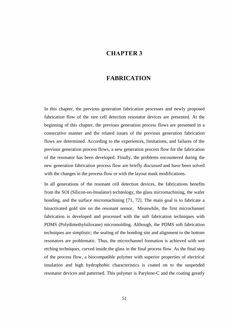
3.1.1 First Generation Process Flow .......................................................................... 55
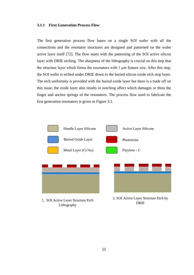
3.1.2 Second Generation Process Flow ..................................................................... 59
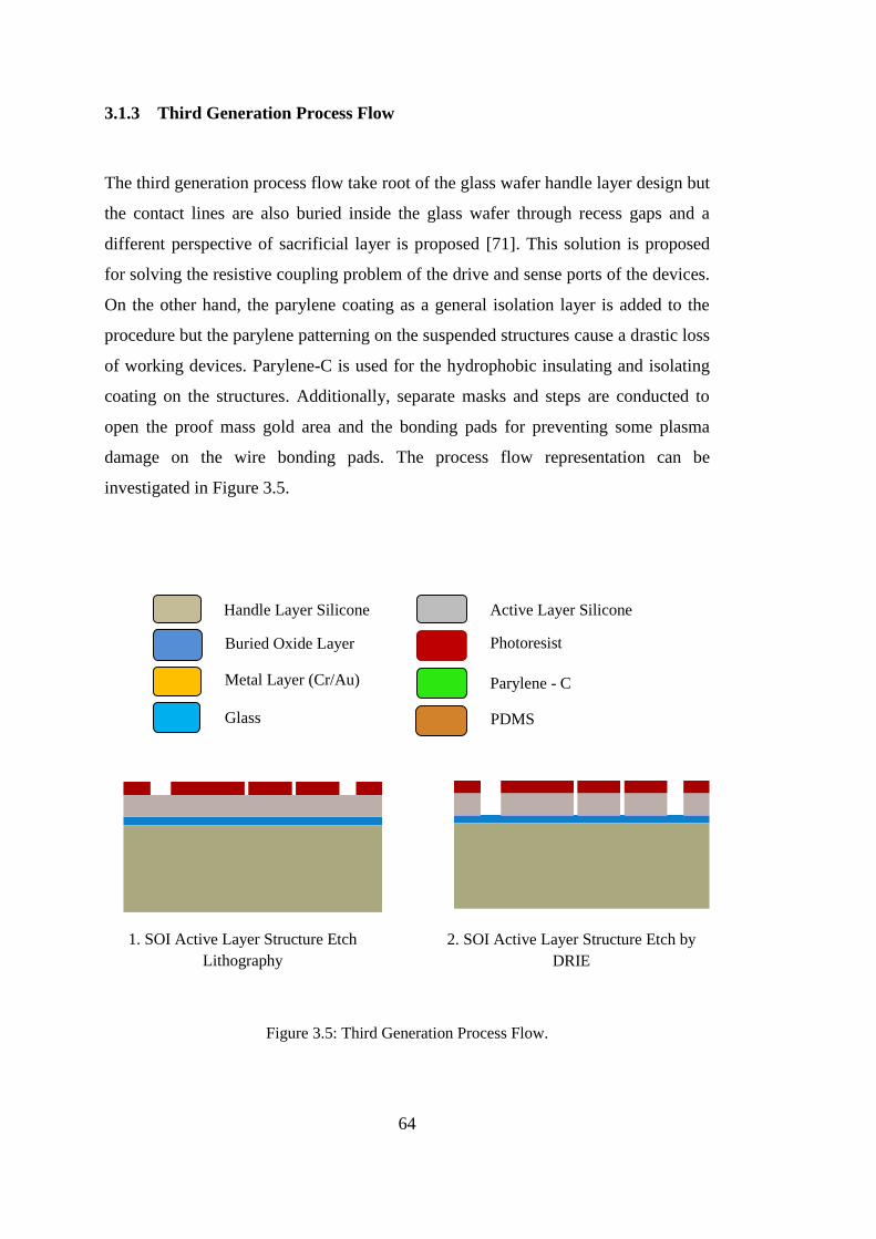
3.1.3 Third Generation Process Flow ........................................................................ 64
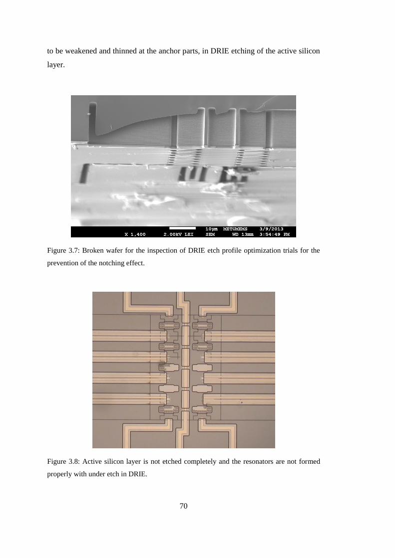
3.1.4 Problems with the Previous Generation Process Flows ........................................ 69
3.2 New (4th) Generation Process Flow ...................................................................... 77
3.3 General Remarks on the New (4th) Generation Process Flow ............................... 89
3.4 Fabrication Summary ............................................................................................ 92
4 EXPERIMENTAL RESULTS ...................................................................................... 95
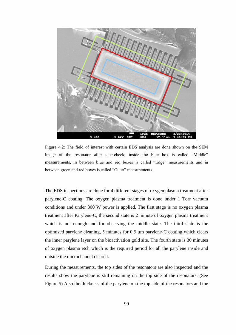
4.1 Parylene Cleaning Except on the Inner Bioactivation Gold Sites ......................... 95
4.2 Interface Circuit .................................................................................................. 103
4.3 Test Results ......................................................................................................... 106
4.4 Fabrication Yield ................................................................................................ 114
4.5 Fabrication Yield Results and Summary ............................................................ 115
5 CONCLUSION AND FUTURE WORK .................................................................... 119
REFERENCES ..................................................................................................................... 123
Page 13
xiii
LIST OF TABLES
TABLES
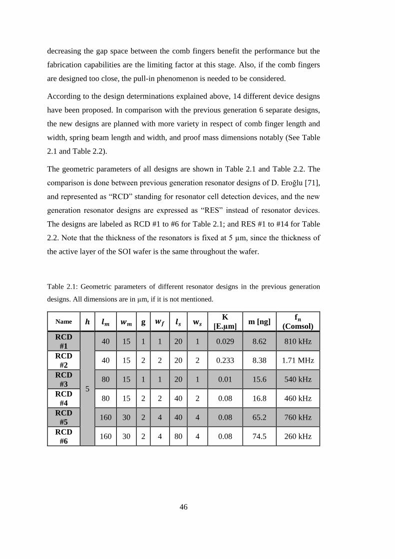
Table 2.1: Geometric parameters of different resonator designs in the previous
generation designs. All dimensions are in µm, if it is not mentioned. ....................... 46
Table 2.2: Geometric parameters of all resonator designs in the final generation (4th
generation) designs. All dimensions are in µm, if it is not mentioned. ..................... 48
Table 4.1: Average values for the percentage of the EDS analysis for 3 different
location intervals. The values are average of 5 measurements each for 6 dies (30
measurements).......................................................................................................... 100
Table 4.2: Comparison for the resonator controlling designs with the previous
generation fabrications ............................................................................................. 111
Page 14
xiv
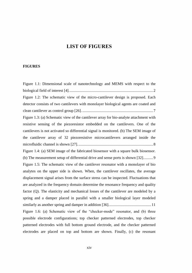
LIST OF FIGURES
FIGURES
Figure 1.1: Dimensional scale of nanotechnology and MEMS with respect to the
biological field of interest [4]. ...................................................................................... 2
Figure 1.2: The schematic view of the micro-cantilever design is proposed. Each
detector consists of two cantilevers with monolayer biological agents are coated and
clean cantilever as control group [26]. ......................................................................... 7
Figure 1.3: (a) Schematic view of the cantilever array for bio-analyte attachment with
resistive sensing of the piezoresistor embedded on the cantilevers. One of the
cantilevers is not activated so differential signal is monitored. (b) The SEM image of
the cantilever array of 32 piezoresistive microcantilevers arranged inside the
microfluidic channel is shown [27]. ............................................................................. 8
Figure 1.4: (a) SEM image of the fabricated biosensor with a square bulk biosensor.
(b) The measurement setup of differential drive and sense ports is shown [32]. ......... 9
Figure 1.5: The schematic view of the cantilever resonator with a monolayer of bio
analytes on the upper side is shown. When, the cantilever oscillates, the average
displacement signal arises from the surface stress can be inspected. Fluctuations that
are analyzed in the frequency domain determine the resonance frequency and quality
factor (Q). The elasticity and mechanical losses of the cantilever are modeled by a
spring and a damper placed in parallel with a smaller biological layer modeled
similarly as another spring and damper in addition [36]. ........................................... 11
Figure 1.6: (a) Schematic view of the “checker-mode” resonator, and (b) three
possible electrode configurations; top checker patterned electrodes, top checker
patterned electrodes with full bottom ground electrode, and the checker patterned
electrodes are placed on top and bottom are shown. Finally, (c) the resonant
Page 15
xv
frequency of checker-mode resonator after coating 12 PEMs bilayers are shown [38].
.................................................................................................................................... 12
Figure 1.7: (a) The probe geometry for the fine sensing, and (b) the optical image of
the probe is shown. The base length L, of the cantilever is made of p-doped silicon
and the L1 length is the ZnO active material coated with Ti/Au. (c) and (d) show the
natural resonance shift of the sensor before (blue) and after (red) the adsorption of
enzyme molecules [39]. ............................................................................................. 13
Figure 1.8: Schematic drawing of the principle of operation of a cantilever with
microchannel embedded inside. (a) Mass of flowing particles is measured using
resonance peak shifts over time under continuous flow of biomolecules, cells or
synthetic particles. (b) While bound and unbound molecules both increase the mass
of the channel, that bind to the channel wall accumulate inside the device. (c)
Another measurement of particles flow through the microchannel of the cantilever
without binding to the surface, and the detected signal changes with the position
along the channel [41]. ............................................................................................... 15
Figure 1.9: (A) Sensor schematic with the first mode of resonance is shown with the
mass sensitivity normalized to its maximum value. (B) SEM image showing sensor
array and (C) measurement setup are presented. (D) Finally, the frequency response
of the sensor with cell attachment (orange), and without (blue) cell attachment are
shown [44]. ................................................................................................................. 17
Figure 1.10: Schematic of the resonator and water droplet containing streptavidin
spotted on the center of biotin modified resonator far from the surrounding
electrodes. [46] ........................................................................................................... 17
Figure 1.11: (a) Schematic view of the U-shaped groove cantilever etched in a SiN
membrane, (b) cross sectional view of the trapping with the meniscus formation on
the bottom of the groove is shown. (c) The resonance spectrum measurements are
shown in air, and (d) after partial wetting under DI water is applied [48]. ................ 19
Figure 2.1: Schematic view of second order mass and loaded biological entity with
two parallel spring and damper systems. ................................................................... 24
Figure 2.2: The representations of microfluidic flows; (a) Couette flow, and (b)
Poiseuille flow [63]. ................................................................................................... 29
Page 16
xvi
Figure 2.3: Schematic view of the overlapping parallel comb finger capacitors is
shown. ........................................................................................................................ 32
Figure 2.4: Schematic view of (a) resonant mass sensor embedded into the
microchannel, and (b) 3-D representation of microfluidic channel and the
bioactivation functionalized on the proof mass gold active area. .............................. 36
Figure 2.5: Schematic view of double folded beam and finger geometries of the
resonator with design parameters are denoted. .......................................................... 38
Figure 2.6: The schematic cross sectional view of the resonator comb finger is shown
with Parylene-C is conformably coated on the suspended components. Thus, the
surface thermodynamic interfacial energy keeps the liquid without any penetration
[69]. ............................................................................................................................ 41
Figure 2.7: The quality factor improvement with parylene coating on the resonator
fingers is shown as a comparison with resonance characteristics of bioresonator in
air, after parylene coating and uncoated performance in water [69]. ......................... 42
Figure 2.8: Fundamental vibration mode of design RES#1 at 1.47 MHz. ................. 43
Figure 2.9: The buckling of the resonators are simulated for gravitational forces. The
maximum buckling displacement at the middle of the proof mass is measured to be
0.1 pm. ........................................................................................................................ 44
Figure 3.1: First Generation Process Flow. ................................................................ 56
Figure 3.2: Illustration of DRIE Notch Effect [74]. ................................................... 58
Figure 3.3: Second Generation Process Flow. ........................................................... 61
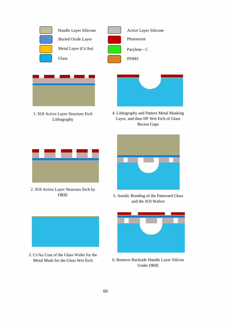
Figure 3.4: PDMS Microchannel Preparation for Second Generation Process Flow. 62
Figure 3.5: Third Generation Process Flow. .............................................................. 64
Figure 3.6: SEM image of the 3rd generation resonator device after DRIE structure is
etched. ........................................................................................................................ 67
Figure 3.7: Broken wafer for the inspection of DRIE etch profile optimization trials
for the prevention of the notching effect. ................................................................... 70
Figure 3.8: Active silicon layer is not etched completely and the resonators are not
formed properly with under etch in DRIE. ................................................................ 70
Figure 3.9: Remaining silicon residue after DRIE etch on the varying etch spaces
without optimization. These residues are the counter issue for the notching effect
which cause loss of the resonator finger and anchor structures. ................................ 71
Page 17
xvii
Figure 3.10: Proper etch on the corner sites of the anchor and fingers after
optimizations are done for the specific structure mask of the resonator features. ..... 71
Figure 3.11: After anodic bonding due to floating areas on the bond surface, high rate
of burning and sparking between fingers of the resonators and metal lines, resulting
in huge amount of loss of the contacts and resonators ............................................... 72
Figure 3.12: (a) Metal routing lines mask can be seen, the die level metal lines are
not connected so at the state of the anodic bonding, there are many floating pads
remaining on the active silicon layer of the SOI and this results in sparking during
the anodic bonding. (b) Metal routing lines mask can be observed for the 4th
generation flow, the die level metal lines are all connected in the new design. Also
there are no floating areas remaining. ........................................................................ 73
Figure 3.13: Rupture oxide regions above bond pads after backside DRIE. [71] ..... 74
Figure 3.14: After the lithography, photoresist penetrated the oxide layer through
microfractures marked with red throughout the wafer and again rupture the oxide
layer after the baking step. ......................................................................................... 75
Figure 3.15: Chromium is etched under long oxygen plasma steps for photoresist
strip and the bioactivation gold site on top of proof mass of the resonators are lifted
off. .............................................................................................................................. 76
Figure 3.16: BHF release wet etch undercut the bond sites glass and the weak spots
like gold connection areas are vulnerable for breakage. ............................................ 76
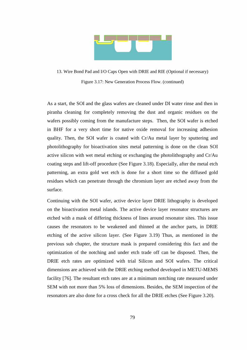
Figure 3.17: New Generation Process Flow. ............................................................. 77
Figure 3.18: Bioactivation metal patterned on clean SOI active layer silicon side. .. 80
Figure 3.19: SOI active layer structure DRIE etch lithography. ................................ 80
Figure 3.20: SEM inspection of SOI active layer structure DRIE etch on the test
resonator. .................................................................................................................... 81
Figure 3.21: Recess etch Cr/Au metal masking layer with Au and Cr layers are
etched. The resonator sites and the tips of the drive, sense and ground lines can be
seen. ............................................................................................................................ 82
Figure 3.22: Recess etch on the glass wafer with metal masking for pure HF wet etch
with 5 µm deepness after the Cr/Au metal masking layer is stripped. ....................... 82
Page 18
xviii
Figure 3.23: The general top view of the resonator mask steps for process flow 3rd
generation. The blue lines show the recess gaps and the metal lines that will be
carved inside the glass wafer. ..................................................................................... 83
Figure 3.24: Microchannel carved inside on the recess patterned glass wafer with 50
µm deep and not more than 170 µm wide. ................................................................. 84
Figure 3.25: Microchannel carved inside on the recess patterned glass wafer with
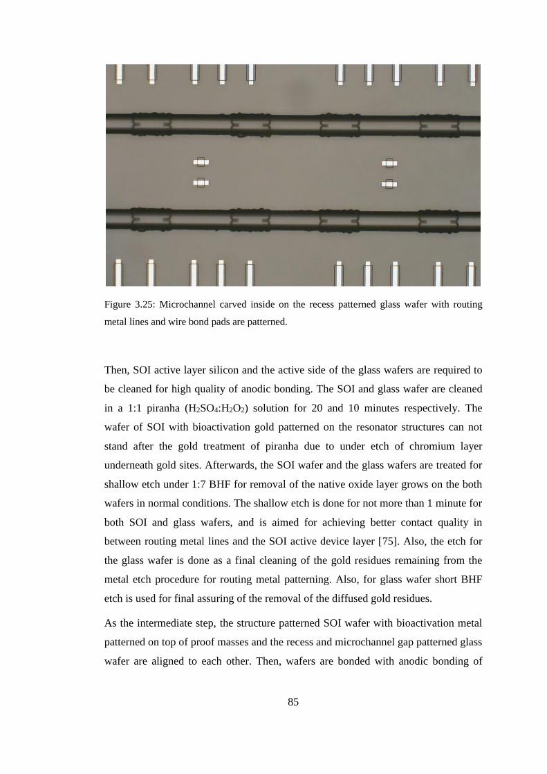
routing metal lines and wire bond pads are patterned. ............................................... 85
Figure 3.26: Resonator sites can be seen after anodic bonding. The microchannel is
carved inside the glass wafer and the bioactivation gold layers are appearing on the
resonators. Sparking is not occurring between fingers of the resonators and it does
not burn off the contact lines. ..................................................................................... 87
Figure 3.27: After the DRIE backside handle layer removal and BHF release are
done. The BHF over etch can be observed around pad contact areas. ....................... 88
Figure 3.28: Gold residues between the fingers and DRIE etch sites due to
penetration challenge of the metal wet etchants in between deep DRIE trenches. .... 90
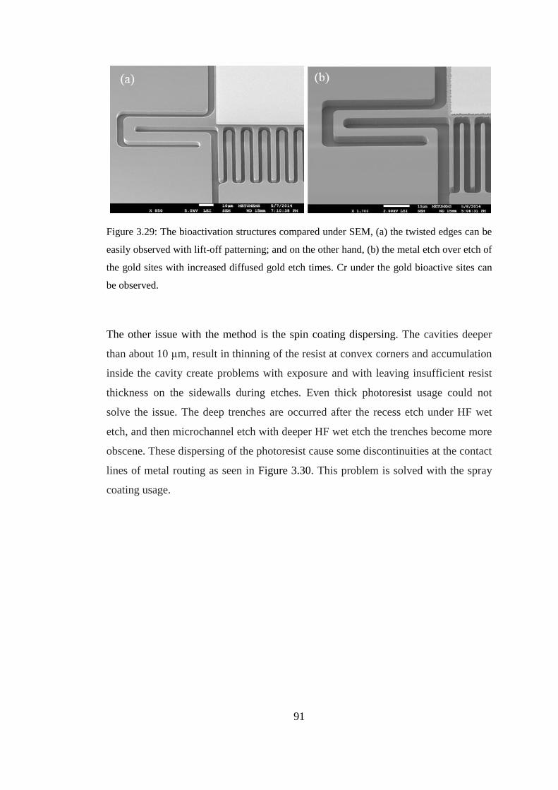
Figure 3.29: The bioactivation structures compared under SEM, (a) the twisted edges
can be easily observed with lift-off patterning; and on the other hand, (b) the metal
etch over etch of the gold sites with increased diffused gold etch times. Cr under the
gold bioactive sites can be observed. ......................................................................... 91
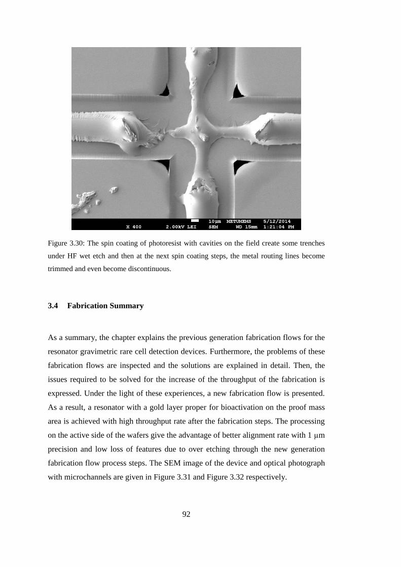
Figure 3.30: The spin coating of photoresist with cavities on the field create some
trenches under HF wet etch and then at the next spin coating steps, the metal routing
lines become trimmed and even become discontinuous. ........................................... 92
Figure 3.31: SEM image of resonant mass sensor device with bioactivation gold is
standing on the proof mass of 4th generation process flow. ....................................... 93
Figure 3.32: The photograph of resonant mass sensor device integrated with
microfluidic channel cap and electrical connections in the 4th generation process
flow. One of the input and output ports are mounted on the holes of the glass
microchannel with white epoxy. ................................................................................ 93
Figure 4.1: The view of the resonators can be observed after tape-check for
observing the inner parylene coating thickness. (a) Parylene is coated and after
oxygen plasma treatment the resonator finger side walls parylene coating still
Page 19
xix
remains in an aspect. (b) If the treatment increased the parylene layer becomes so
thin that the SEM blur created cause of the insulation of parylene disappears.......... 98
Figure 4.2: The field of interest with certain EDS analysis are done shown on the
SEM image of the resonator after tape-check; inside the blue box is called “Middle”
measurements, in between blue and red boxes is called “Edge” measurements and in
between green and red boxes is called “Outer” measurements. ................................. 99
Figure 4.3: The measurements for the thickness are not reliable but it gives
information about the average thickness distribution. (a) The measurement of
thickness of the parylene layer on the resonators from the top view before the oxygen
plasma treatment is around 0.45 µm, after the oxygen plasma treatment (b) resonator
coating thickness is dropped to 0.31 µm. ................................................................. 101
Figure 4.4: The resonator devices are shown under optical microcope, (a) after
parylene coating, (b) after parylene is etched with short oxygen plasma treatment. (c)
and (d) are the focused images for parylene coated and plasma treated devices
respectively. ............................................................................................................. 102
Figure 4.5: Resonator measurement setup is shown, with the network analyzer, DC
supplies, and the interface TIA circuit. The device is measured with the network
analyzer under probe station. The measured devices and the read-out circuit with TIA
interface integrated are identified in green circles. .................................................. 105
Figure 4.6: The magnitude and phase measurements of (a) the resonator without
coating and (b) with parylene coating are done for RES #7 device by direct
observation of network analyzer. The shift of natural frequency is observed from
572.8 kHz to 563.2 kHz after parylene coating. ...................................................... 107
Figure 4.7: The capillary flow test is done with injecting DI water with syringe from
one end of the microchannel and without any leakage water come out from the other
end of the microchannel ........................................................................................... 108
Figure 4.8: The mass of parylene can be observed with shift of resonance peak of the
gravimetric resonator sensor. The resonance frequency is shifted down from 229.3
kHz (green) to 221.5 kHz (red) and the quality factor is also decreased from 764.3 to
573.0. The resonator with parylene coating under fluid flow shows 221.6 kHz
resonance frequency and the quality factor drop to 198.4. ...................................... 109
Page 20
xx
Figure 4.9: The magnitude and phase components of the resonance characteristics of
RES #1 design with 44 x 16 µm2 proof mass area and with natural frequency of 806
kHz and quality factor of 289. .................................................................................. 112
Figure 4.10: The magnitude and phase components of the resonance characteristics
of RES #13 design with 248 x 128 µm2 proof mass area and with natural frequency
of 232 kHz and quality factor of 862. ...................................................................... 113
Figure 4.11: The wafer map with numerical representation of 64 dies with 14
different architectures of resonators are placed. ....................................................... 116
Page 21
1
CHAPTER 1
1 INTRODUCTION
The future of MEMS relies on the new efforts to develop micromachined
components for the governance of microfluidic systems are just beginning to bear
fruit. The biological opportunities on the MEMS field are expected as the driving
factor for next decade [1]. When the sizes of the biosensors shrink to the cell level,
the sensing of a living cell becomes the attracting field of interest where the rare cell
detection which is specialized for selective sensing, trapping, isolation and inspecting
the cell. The properties like mass, volume, density and deformability of living cell
are required to be precisely measured with the new tools in hand. The integration of
micropumps with microvalves and reservoirs to build new miniaturized biosensing
and delivery systems are under radar for research [2].
This thesis is specialized on a certain kind of rare cell detection with a gravimetric
resonator structure. Thus, the thesis will take a brief underline for the concept and
focus on the cell detection applications particularly the mass sensing of the living cell
in fluid environment.
In this chapter, BioMEMS is briefly explained, basically focusing on the cell
detection applications with different detection methods. The proposed sensor is a
gravimetric resonant biosensor, so the chapter is narrowed down to especially on
gravimetric detection techniques for cell detection applications. At the end, yield
tracking for MEMS fabrication process flows is also mentioned.
Page 22
2
1.1 Introduction to BioMEMS
Biomedical Microelectromechanical Systems (BioMEMS) is defined as “devices or
systems, constructed using techniques inspired from micro or nanoscale fabrication,
that are used for processing, delivery, manipulation, analysis, or construction of
biological and chemical entities” that Rashid Bashir famously stated [2].
Conventional commercial instruments for medical, biochemical, and genetic analysis
perform a broad range of analytical functions but are generally bulky. The general
aim to miniaturize all aspects of biochemical analysis is flourished with the concept
of micrototal analysis system (μTAS) or Lab on a Chip (LoC) system, which was
introduced in 1989 by Manz [3]. The terminology makes little difference; the basic
fact is the BioMEMS technology emerged from the requirement of achieving
micrometer level medical laboratories. The biological analytes under the interest of
biology and medicine; like cells, proteins or viruses, have micrometer or even
nanometer level sizes. Thus, the transducer of the sensor device should also be at
comparable sizes (See Figure 1.1).
Figure 1.1: Dimensional scale of nanotechnology and MEMS with respect to the biological
field of interest [4].
Page 23
3
The major advantage of MEMS technology is the opportunity of designing and
producing miniaturized systems. The shrinking of the sizes of operational devices is
permitting the systems to be fabricated with low die budget, mass produce capability
and lower power consumption. Likewise, these new micro level biodevices of
BioMEMS decrease the manufacturing costs, increase reproducibility, enhance
controllability, and also lower the sample size and the reagent use. The signal to
noise ratio and response time improves with these micro devices. The other
advantages are precise control of mixing, reaction rate, enhanced heat transfer,
discarding waste products, enabled point of care diagnosis, improved safety with
experiments and also possibility of embedded detection methods and high throughput
rate [5].
BioMEMS devices are analytical devices that integrate a biosensitive factor with a
physical or chemical transducer for selectively and quantitatively detect the
biological compounds in a specified environment. μTAS or LoC devices are used for
delivery, processing, analysis, or detection of biological molecules and species [1].
These devices are used to detect cells, microorganisms, viruses, proteins, DNA and
related nucleic acids, and small molecules of biochemical importance and interest.
The studies of BioMEMS can be separated into diagnostic and therapeutic devices
[6]. The diagnostic systems study the analysis, separation, and characterization of the
biological analytes [7], alternatively the therapeutic systems work on implantable
biocompatible devices for the living organisms like implants [8], neural interfaces
[9], and drug delivery systems [10].
Generally the BioMEMS devices are integrated with tubings and channels.
Microfluidics operation is critical in order of the biological and medical analysis
studies with examination samples in fluidic environments. The biocompatibility is
critical with the microchannel in tube material or coating; due to the interaction with
the biological elements in the fluid. PDMS (Polydimethylsiloxane) [11] and Parylene
[12] patterned structures are both biocompatible and they are best fit for the
microchannel fabrication of BioMEMS devices. Processing of BioMEMS devices
using polymeric devices and soft lithography is very attractive due to increased
Page 24
4
biocompatibility and easy fabrication, ability to integrate functional hydrogel
materials, and low cost and rapid prototyping methods available in polymer based
materials [13].
Cells consist of 70% water and the cell can not survive out of liquid environment for
an adequate time. Among these advantageous properties of BioMEMS, the sensing
and actuation of living cells under fluidic medium, mostly with water and blood is
the prominent field. The recent emerges of the techniques of the BioMEMS enables
us to detect under these targeted environments [14].
1.2 BioMEMS Methods for Cell Detection
The living cell detection is one of the most promising fields of BioMEMS which
includes; ability to detect a specific cell inside a population of cells, and ability to
deal with very small sized samples like even receptive biomolecules. These demands
can be only solved with high sensitivity, high accuracy, high selectivity, and high
throughput of cells under medium. Cellular analysis supports many fields including
drug discovery, diagnostics, cancer research, regenerative medicine, system and
synthetic biology, and renewable energy [1].
The implementation of microfluidic technologies in single cell analysis is one of the
most promising approaches that not only offers information rich, high throughput
screening but also enables the creation of innovative conditions that are impractical
or impossible by conventional means. The possibilities for distinguishing the
difference between individual cells and the benefits from miniaturization have led to
many discoveries both in traditional biopharmaceutical communities and in emerging
fields such as synthetic biology [3].
Physical applications of cell sorting and isolation are examined as the first elevation
for the BioMEMS cell analysis applications. These applications are mostly fluidic
setups with certain geometries and the separation of cells with respect to their
volume, mass and density can be easily implemented as LOC apparatuses. In this
way, size based capture and separation [15], identification and counting [16], with
Page 25
5
geometry manipulations under changing flow, and electrophoresis and
dielectrophoresis applications with the use of electrokinetic forces [17] are used for
cell detection and analysis [18].
Although, these kinds of applications of BioMEMS show a great promise for the
future with simple designs of biochips with microarray architectures; the transducer
based biosensor applications create the possibility of straight to the point sensing
[19]. The biosensor based devices stand on detection methods of BioMEMS which
can be narrowed down to four fields; electrical [20, 21], electrochemical [22, 23],
optical [24, 25], and mechanical detection [26, 27].
The electrical detection technique relies on the electrical impulse caused of current
change due to conductance, impedance and RF parameter manipulations with the
sensor. The method minimizes the sensing field and enables label free detection that
the direct interaction between analyzed medium and the sensor is possible. In this
way, the sensitive agent is directly attached to a transistor, a resistor of a MEMS
circuit that measures the electrical parameters of the sample [13]. The electrical
detection is similar to electrochemical detection without any chemical reactions
taking place in the medium. The effect of conductance or impedance change is
directly result from the change of the electrical characteristics of the analyte or in RF
case, the analyte is placed so that the magnetic effect causes a disturbance of the
permittivity or permeability.
The electrochemical sensors are very similar to the electrical sensing applications.
The only difference is a chemical reaction is occurring on the site of sensing. This
reaction causes a direct actuation for the biosensor in respect of current, voltage or
conductance. The electrochemical detection of BioMEMS application mostly sense
the redox reactions and changing ion concentration in the medium. The main
advantage of the electrochemical detection is simplicity and though cheap
applications for BioMEMS with label free detection. The electrical sensing without
any complex analysis tool decrease the response time and even real time sensing is
possible. On the other hand, the data analysis can be an issue with many chemical
reactions other than desired sensing entity occurs at the same time which causes data
Page 26
6
ambiguity. The solution is cross checking the data with other detection tools like
optical or mechanical detection equipments for calibration or optimization.
Optical detection mechanism makes use of change of optical entities like UV
absorption, luminescence, and reflectance [28]. Additionally, the interferometry is
applied to bio-analytes for detection applications with the use of refractive index
differentiations on the biosensitive thin film [29]. Many nowadays used monitoring
device for medical applications are based on the optical detection mechanisms so the
background of these applications is well defined and most of the BioMEMS optical
applications are miniaturized systems with similar working principles with the
original counterparts. Nonetheless, optical biosensors offer several advantages such
as sensitivity, flexibility, resistance to electrical noise and high stability. Actually, the
bulky structure of the optical sensing setup with extra observation tools required, the
area gives space for new novel designs.
In this thesis the proposed design is a gravimetric sensor so focus is on the
mechanical detection mechanisms for biosensor based rare cell detection
applications.
1.3 Mechanical Detection
The mechanical detection techniques rest ground on stress and mass detection
techniques. The cantilever structures are the main component for the widely used
mechanical detection applications for BioMEMS. The bending of the cantilever is
the transducing factor measured with the help of position detector like AFM or laser
or electrical means like piezoresistor established on the cantilever. Stress sensitivity
of the cantilever is inversely proportional to the spring constant while the overall
surface of the cantilever determines the number of molecules that can attach to the
surface to cause a resulting stress change. The change is measured with the
resonance characteristics of the design at this time [5]. Cantilever based systems are
capable of real-time, multiplexed detection of unlabeled disease markers in
extremely small volumes of samples. Nowadays fabrication techniques will allow the
integration of electronic readout and sample introduction into a single unit,
Page 27
7
decreasing the device size, detection time, and cost. Biosensor technologies based on
fabricated cantilever arrays involving multiple cantilevers, electronic processing, and
even local telemetry on a single chip have the potential of satisfying the need for
highly sensitive and selective multiple-target detection in very small samples.
The design of the cantilever array structure is a label free surface stress sensor with
two identical sensors with one of them is working as a reference detector [26]. The
other detector is coated with self-assembled monolayer of binding agents (See Figure
1.2). Also, the study examines the appropriate biocantilever with comparative study
of Si, AlN, SiN and PMMA (Polymethylmethacrylate); and found out that the higher
sensitivity and biocompatibility lead to PMMA is the suitable material for this
application. The system is also tested for self-assembly monolayer of yeast cells.
Figure 1.2: The schematic view of the micro-cantilever design is proposed. Each detector
consists of two cantilevers with monolayer biological agents are coated and clean cantilever
as control group [26].
Another study focuses on the instrumentation of the piezoresistors fabricated on
silicon micro cantilevers and measuring the bending of the cantilever array [27]. A
minimum detectable surface stress change of 2.6 mN/m is measured with
immobilization of single stranded thiol modified DNA oligonucleotides (See Figure
1.3). Also, it is demonstrated that analyze of two samples simultaneously by utilizing
Page 28
8
the laminar flow in the microfluidic channel system with controlled directionality is
possible.
The mechanical biosensors are also fabricated with different base materials like thin
membrane of PDMS with bi-membrane concept [30]. The study shows a low cost
design with easy fabrication steps for a large active functionalization area for
biological analyte binding and the bending of the PDMS is sensed by a capacitor
which one electrode is placed on the PDMS membrane and the other onto the base
substrate. The stress based sensors are further reviewed by the study of Sang et al.
[31] in detail with state of the art applications.
Figure 1.3: (a) Schematic view of the cantilever array for bio-analyte attachment with
resistive sensing of the piezoresistor embedded on the cantilevers. One of the cantilevers is
not activated so differential signal is monitored. (b) The SEM image of the cantilever array
of 32 piezoresistive microcantilevers arranged inside the microfluidic channel is shown [27].
The second portion of mechanical biosensors senses the mass of the analyte directly
with shift of the resonance characteristics of the resonator structure. In the study [32],
Heidari et al. present the a biosensor with a micromachined silicon squared plate that
is excited in the Lamé bulk acoustic resonant mode at a frequency of 37.8 MHz, and
with quality factor of 10,000 and the mass sensitivity of 400 Hz/pg (See Figure 1.4).
In another study by Liu et al. [33] the biosensor system includes two biosensing
techniques; resonant frequency measurements and electric cell substrate impedance
sensing (ECIS) on a single device. The double sensor system integrates the upper
Page 29
9
electrode of a quartz crystal microbalance (QCM) resonator and a active site as
working microelectrode for ECIS technique. The hybrid device is successfully used
for Bovine aortic endothelial live cells. This method can be implemented to water
toxicity detection apparatuses. Likewise, the study of Huang et al. [34] is based on
QCM resonators which are used as a maize chloratic mottle virus biosensor is
compared to the commercial enzyme linked immunosorbent assay (ELISA) test
methods. Moreover, in the study of Gruhl et al. [35], the surface acoustic wave
(SAW) biosensor is used for label free detection of Penicillin G in milk and the
system gives satisfactory results for commercial limits of European Commission.
Figure 1.4: (a) SEM image of the fabricated biosensor with a square bulk biosensor. (b) The
measurement setup of differential drive and sense ports is shown [32].
1.4 Gravimetric Detection for Cell Sensing
The gravimetric detection technique is one of the sub topics of mechanical detection
related with the mass detection. Briefly, the gravimetric detection technique depends
on the change of resonance frequency of an oscillating mass, when the resonator
mass changes. When extra mass is added on the oscillating structure, the natural
frequency of the resonator alters [36]. Actually, the damping coefficient and the
spring constant of the gravimetric resonator system also change when a mass is
added on the proof mass of the resonator. However, the change caused by this
loading can be considered negligible for most of the applications. The relationship
between the natural resonance frequency (f) and the resonator mass (m) is given in
Page 30
10
Equation (1.1), where k is the spring constant of the resonator. Also, the mass change
can be calculated from the relation between resonator shifted frequency (fl) and the
initial unloaded natural frequency (f0) as seen in Equation (1.2). The quality factor
(Q) of the resonance characteristic can be defined as in Equation (1.3). The basic
cantilever operation as a gravimetric sensor is explained in Figure 1.5.
As mentioned for mechanical detection applications, the gravimetric technique also
relies mostly on cantilever structures. However, other kinds of resonator structures
are starting to arouse interest for the past decade [37]. Generally, the operation
principle of the gravimetric sensor is that the resonator is driven at its resonance
frequency where the resonance dynamic response amplitude is at its peak. The
driving methods include piezoelectric actuators, magnetic forces, and light-induced
forces.
𝑓 =1
2𝜋√
𝑘
𝑚
(1.1)
∆𝑚 =k
4𝜋2 √1
𝑓𝑙2 −
1
𝑓02
(1.2)
𝑄 = √3f0
∆f
(1.3)
Page 31
11
Figure 1.5: The schematic view of the cantilever resonator with a monolayer of bio analytes
on the upper side is shown. When, the cantilever oscillates, the average displacement signal
arises from the surface stress can be inspected. Fluctuations that are analyzed in the
frequency domain determine the resonance frequency and quality factor (Q). The elasticity
and mechanical losses of the cantilever are modeled by a spring and a damper placed in
parallel with a smaller biological layer modeled similarly as another spring and damper in
addition [36].
The cell detection applications require high degree of sensitivity for perceiving very
low amount of mass changes. The gravimetric detection with high performance
resonator based designs show that detection of even one cell with high precision of
the mass amount quantitatively and selectively. Thus, the gravimetric detection
becomes the promising field of interest, and is successfully used for rare cell
detection among much different cell diversity.
The PZT based piezoelectric gravimetric biosensors have the high detection
performance for rare cell detection applications. In the study of Heidari et al. [38] a
AlN piezoelectric resonator with checker patterned electrode is fabricated for mass
Page 32
12
sensing applications (See Figure 1.6). Three different electrode architectures are
shown in the schematic differing for the placement of electrodes on the top side, both
sides, and the ground electrode addition to the backside. The device shows a mass
sensitivity of 175 µm2/ng and 18.7 ng/cm2 detection limit when polyelectrolyte
multilayer (PEM) polymer is coated on the resonator structures and then, the
resonance shift is monitored [38].
Figure 1.6: (a) Schematic view of the “checker-mode” resonator, and (b) three possible
electrode configurations; top checker patterned electrodes, top checker patterned electrodes
with full bottom ground electrode, and the checker patterned electrodes are placed on top and
bottom are shown. Finally, (c) the resonant frequency of checker-mode resonator after
coating 12 PEMs bilayers are shown [38].
Page 33
13
In another study, based on the Euler-Bernoulli Beam Theory, a PZT gravimetric
cantilever geometry is applied to very small mass sensing in the means of enzyme
molecules immobilized on the sensor surface [39]. The design geometry and the
sensitivity results are shown in Figure 1.7. Finally, a wireless magnetoelastic
gravimetric sensor is developed for sensing Salmonella cell cultures, which is a kind
of biological contamination for tomato [40]. The system can be used for level of
contamination on site and real time.
Figure 1.7: (a) The probe geometry for the fine sensing, and (b) the optical image of the
probe is shown. The base length L, of the cantilever is made of p-doped silicon and the L1
length is the ZnO active material coated with Ti/Au. (c) and (d) show the natural resonance
shift of the sensor before (blue) and after (red) the adsorption of enzyme molecules [39].
One of the leading studies in the field of gravimetric rare cell detection was
presented by Burg et al. [41]. The resonator cantilever structure includes the
microchannel inside the suspended structure. The working principle is that the
solution flows in the channel embedded hollow resonator and the cantilever can work
under vacuum environment for achieving high resonance quality factor. The group
Page 34
14
demonstrates that by using suspended microchannel resonators, even single
biological nanoparticles, bacterial cells and sub-monolayers of adsorbed proteins can
be identified inside DI water. The structure and the measurement procedure is
explained briefly in Figure 1.8. Also, resolution at the level of femtograms is
reported with less than 1 Hz measurement bandwidth. The working opportunity
under vacuum eliminate also the air damping issue, and it is shown that the viscous
fluid damping is negligible compared to inner dissipation of energy inside cantilever
microchannel. However, this method is not applicable for medium sized cells and
other particles, that the cells will be stuck inside the microchannel because of
crowdedness.
Another study by Poshtiban et al. [42], presents a microresonator array platform that
uses phage tail spike proteins as a recognition probe. This array is composed of one
thousand active beams in 13.5 mm2 area for high capture rate of bacteria cells. The
resonators have natural frequency at 1.095 ± 0.005 MHz and minimum mass
sensitivity of 52 fg. This device demonstrates the usage of these beams with specific
detection of the Campylobacter jejuni cells after immobilization of devices with
phage GST-Gp48 tail-spike proteins. On the other hand, the functionalized device
active areas do not show any sensitivity to Escherichia coli bacteria which confirms
the specificity of the detection [42].
Page 35
15
Figure 1.8: Schematic drawing of the principle of operation of a cantilever with
microchannel embedded inside. (a) Mass of flowing particles is measured using resonance
peak shifts over time under continuous flow of biomolecules, cells or synthetic particles. (b)
While bound and unbound molecules both increase the mass of the channel, that bind to the
channel wall accumulate inside the device. (c) Another measurement of particles flow
through the microchannel of the cantilever without binding to the surface, and the detected
signal changes with the position along the channel [41].
The final group of studies is well known application of droplet investigation
technique led by R. Bashir’s group [43-45]. In one of the first studies [43] the rare
cell mass detection by trapping and immobilizing the cell on cantilever based
resonator systems, and then, the observation is done under optical equipment. They
inject HeLa cells inside of a microfluidic channel and capture the cells on the
cantilevers using positive dielectrophoresis. Then, the immobilized cells are dried or
cultured at the site of the cantilever array in order to make the measurements.
Afterwards, standing on the same concept, cantilever is replaced with a MEMS based
mass sensor and the cell growth is monitored for more than 50 hours [44]. Analysis
shows that resonating platform designs demonstrate spatial non-uniformity of mass
sensitivity or error due to cell position to be less than 4% from the center to the edge
of the platform. The structure of the biosensor, measurement setup, and frequency
response is presented in Figure 1.9.
Page 36
16
One of the newest studies on this method is microdroplet evaporation process with
the mass changes during the evaporation of the dimethylsulphoxide and water [45].
By this way, the study validates the possibility of investigation of microscaled
physical processes and biological phenomena involving evaporation and mass
transport. However, these studies require Lorentz force actuation for resonator
sensing components and complex laser systems for observation. Therefore, the
system is not practical for usual medical detection.
In a similar study, the water droplet is put on the biotin functionalized resonator
device without leakage to the surrounding electrodes on the sides of the resonator as
shown in Figure 1.10. It is demonstrated that the capacitive detection of the biotin
and streptavidin binding with the mass sensitivity level is 87.76 µm2/ng in aqueous
environment [46]. Besides, the sensor surface immobilization of biotin molecules
took place directly on the silicon surface using APTES. The developed sensor can be
used to observe the interaction between biotin and streptavidin without the use of
labeling or molecular tags. Thus, the method is applicable for a variety of different
immunoassay tests.
Page 37
17
Figure 1.9: (A) Sensor schematic with the first mode of resonance is shown with the mass
sensitivity normalized to its maximum value. (B) SEM image showing sensor array and (C)
measurement setup are presented. (D) Finally, the frequency response of the sensor with cell
attachment (orange), and without (blue) cell attachment are shown [44].
Figure 1.10: Schematic of the resonator and water droplet containing streptavidin spotted on
the center of biotin modified resonator far from the surrounding electrodes. [46]
Page 38
18
1.4.1 Controlling Damping
The fluidic damping is the main obstacle for the resonator operation under fluidic
environment which degrades the performance even to the nullity level. Thus, before
closing the chapter, a literature survey for the techniques used for reducing the
damping effect is given.
In the study [47] by Joshi et al. the general approaches for lowering or even
eliminating different types of damping effects for the basic resonator applications are
summarized. As mentioned before, the major gravimetric sensing mechanisms utilize
cantilever based structures so most of the solutions are enhanced for cantilever
applications.
One of the state-of-art methods for prevention of damping under fluidic operation is
stated by Linden et al. [48], that the adaptation of the fluid interface with a meniscus
formation benefits the performance considerably. In the study, a U-shaped design is
etched in silicon nitride layer and the meniscus like membrane cantilever is working
as a trap for a certain volume of water droplet on the top of the U-shaped cantilever.
The schematic representation is shown in Figure 1.11 and the trapping or partial
wetting can be observed on top of the silicon nitride cantilever. The sensitivity in DI
water flow is measured to be 2.77 fg/Hz, and also the resonance characteristics are
shown in Figure 1.11.
Page 39
19
Figure 1.11: (a) Schematic view of the U-shaped groove cantilever etched in a SiN
membrane, (b) cross sectional view of the trapping with the meniscus formation on the
bottom of the groove is shown. (c) The resonance spectrum measurements are shown in air,
and (d) after partial wetting under DI water is applied [48].
In another study, a micro level drumhead like structure with a hole in the middle of
the design is presented for the degradation of squeeze film damping under fluidic
sensing environment for acoustic radiation [49]. For a narrow band of acoustic
frequencies the specific damping issue is solved with the design but it can not be
implemented to common practice of resonator geometries in fluidic applications.
Furthermore, Cranch et al. show that the low frequency (𝜔 ≤ 1𝑘𝐻𝑧) driven
cantilevers are less affected by damping in viscous fluid environments [50]. In
another study, the geometry of the cantilevers are manipulated differing from the
standard rectangular suspended design [51] and even the placement of the active sites
are examined for lowest optimized damping impact [52]. Besides, the advantages of
the laterally oscillating cantilevers are shown in fluid mediums with considerable
quality factor improvements and with lower limits of mass detection [53].
Page 40
20
1.5 Research Objectives and Thesis Outline
In this thesis, the development of a high yield fabrication method for the predesigned
gravimetric resonator sensor devices is shown. As the main advantage, the resonators
are capable of operating under fluidic flow inside biocompatible microfluidic
channels. The newly proposed fabrication flow takes the problems existing for the
previous generation cell detection resonator devices into account and by introducing
a new approach for the fabrication with the main aim of increasing the fabrication
yield considerably. The principal objectives of the thesis are listed below.
The fabrication process flow will be improved with easily workable process
steps and eliminating the wet processes applied on the suspended devices.
Moreover, the new fabrication flow considers improving each step one by
one, and so the total yield of the fabrication increases.
The strengthened folded spring anchors and design modifications is aimed to
decrease the breakage rate so the endurance of the resonators during
problematic fabrication steps is increased from start to end.
The resonators’ operationality is intended to be sustained under fluid flow.
Therefore, successful hydrophobic parylene coating between fingers and
anchors needed to be established. At the same time, the field of the
bioactivation gold needs to be cleared for functionalization protocol to
immobilize selectively the intended cells after the hydrophobic film coating.
Hence, the rare cell detection with the gravimetric resonators is achieved.
This issue is aimed to be solved with a novel parylene coating method.
Finally, the new process flow intends to solve the poor PDMS microchannel
architecture. The new fabrication method makes use of an anodic bonded
glass microchannel with high opportunity of controlling the alignment with
respect to the resonators. The anodic bonding process will seal the
microchannel with a negligible leakage. Lastly, the glass microchannel will
present better optical transparency compared to the PDMS microchannel
architectures.
Page 41
21
The thesis focuses on;
In chapter 2, the necessary theoretical background to analyze the operation of
micromechanical resonators is given. The characteristics of the MEMS actuators
with capacitive actuation and the microfluidics theory are explained. Next, the
theories behind the sensing mechanisms of a gravimetric sensor, movement of the
mechanical structure, folded spring beams, and damping issue on the structure are
given. Finally, the design parameters of the devices are optimized together with
COMSOL finite element analysis results.
Chapter 3 summarizes the fabrication process development of the resonators.
Previous fabrication process flows and the newly proposed process flows are
inspected. The advantages and disadvantages are presented with the solutions of the
issues. Implemented solutions to the previous generation fabrication flows are
summed up in the new generation fabrication process flow with a newly introduced
approach to fabrication. Finally, the problems encountered during the new process
flow are submitted with the solutions for the issues.
Chapter 4 starts with the novel method of parylene hydrophobic coating trials.
Afterwards, the experimentation and test results are presented. First, the experimental
setup and test environment is briefly introduced. Then, the results of various tests
such as resonance characterization with and without parylene coating are presented.
The results are compared with the previous generation cell detection studies of the
METU BioMEMS group.
As the closure, conclusions and future works are presented in Chapter 5.
Page 43
23
CHAPTER 2
2 THEORY & DESIGN
In this thesis, the proposed resonator structure is basically an electrostatic capacitive
comb drive resonator with folded spring beams. Thus, the study is narrowed down to
these operation principles of the comb drive resonator structures from now on.
Capacitive comb drives are used in many different applications in the literature
including charge sensors [54], microgrippers [55], gyroscopes [56] and
accelerometers [57].
In this chapter, an introduction for gravimetric detection is summarized. Then, the
theoretical background and the operation principles of the BioMEMS group
resonators are stated. Finally, the device characteristics and major trade-offs of the
design parameters are described, and through this examination the optimized limits
of parameters for the device are stated.
2.1 Gravimetric Detection
The gravimetric detection concept relies on the change of the natural frequency, of
the resonator, when the resonator mass changes. There is an inverse quadratic
relation between the resonance frequency of the system and the oscillating mass of
the resonator. Actually, the spring constant and the damping coefficient of the
resonator system changes but the transition remain at a negligible level for most
gravimetric sensing systems.
Page 44
24
The resonator sensor beam can be examined as a mass, damper and spring system as
represented in Figure 2.1, in this representation the biological load is also added as
an added smaller spring, damper and spring system installed in parallel with the main
mass, spring and spring system. Where kres and kbio represents the spring constants,
ηres and ηbio denotes the damping constants and mres and mbio represents the
resonating mass for resonator sensor and the biological analyte respectively. The
springs accumulate force and the dampers dissipate the force in the system [5].
Figure 2.1: Schematic view of second order mass and loaded biological entity with two
parallel spring and damper systems.
The following equation describes the second order behavior of this system;
𝑚�̈� + 𝜂�̇� + 𝑘𝑥 = 𝐹 (2.1),
where x identifies the proof mass displacement, F represents the applied force, m
stands for the system mass, η is the damping constant, and k is the spring constant.
The gravimetric resonator system is a linear and time-invariant system, so we can
Page 45
25
take the Laplace transform of the above equation to obtain the transfer function of
the system as applied in Equation (2.2) [58].
𝐻(𝑠) =1
𝑚𝑠2 + 𝜂𝑠 + 𝑘
(2.2)
Then, we can identify the natural frequency 𝜔𝑛 of the system as in Equation (2.3);
𝜔𝑛 = √𝑘
𝑚
(2.3)
The shift of the resonance frequency of the resonator (𝜔𝑑) from the natural
frequency (𝜔𝑛) is caused by the damping applied on the system [59] as in Equation
(2.4).
𝜔𝑑 = 𝜔𝑛√1 − 𝜉𝑑2
(2.4)
where 𝜉𝑑 is the damping ratio, and defined as in Equation (2.5).
𝜉𝑑 =𝜂
2√𝑚𝑘 (2.5)
If the damping ratio is higher than 1 (𝜉𝑑 > 1), from the Equation (2.4), the frequency
of oscillation will become complex [60]. In this case, the system is called to be over-
damped and the resonance peak will be degraded. If it is smaller than one (𝜉𝑑 < 1),
the system is called under-damped and the resonance oscillation frequency becomes
closer to the natural resonance frequency where the damping ratio gets even smaller.
If the damping ratio is equal to 1 (𝜉𝑑 = 1), then critical damping state occurs, and the
natural frequency asymptotically approach to zero.
Furthermore, in mass sensing applications, the parameter that indicates the resonator
performance is the quality factor; Q. For resonance applications, quality factor is the
parameter that indicates how much the system is under-damped. In other words, the
quality factor expresses the dissipation of energy due to damping from the total
stored energy of the resonating system. Therefore, resonance oscillations vanish in a
slower manner caused of damping when the quality factor increases. The general
Page 46
26
definition of the quality factor is defined as in Equation (2.6) by the means of energy
E and so Equation (2.7) is derived.
𝑄 = 2𝜋𝐸
∆𝐸
(2.6)
𝑄 =1
2𝜉𝑑√1 − 𝜉𝑑2
(2.7)
For this study, the damping ratio is much smaller than 1 (𝜉𝑑 ≪ 1). Thus, Equation
(2.7) can be simplified into Equation (2.8).
𝑄 ≅1
2𝜉𝑑=
√𝑘𝑚
𝜂
(2.8)
When Equation (2.8) is analyzed, 𝑄 is a parameter that can be calculated from the
resonance frequency spectrum measurement result in a very narrow frequency range.
Firstly, the resonant frequency 𝜔𝑛 is measured and then, the amplitude 𝐴𝑟 at the
resonance frequency is expressed. Then, the amplitude and frequency parameters
around the resonant frequency with -3 dB low amplitude margins 𝜔1 and 𝜔2 are
measured. Finally, the quality factor (𝑄) can be calculated by the reinterpretation of
Equation (1.3);
𝑄 = √3ω0
𝜔1 − 𝜔2 (2.9).
2.1.1 Damping Mechanisms
The quality factor of the gravimetric resonators is decreased mostly by the energy
dissipation of the damping effects of the resonator relation with the environment.
Broadly speaking, the damping mechanisms fall into two main categories; fluid and
structural damping. The fluid damping is divided into viscous and acoustic radiation
based damping and the structural damping is separated into thermo elastic damping
(TED) and anchor loss [61]. Thus, the lowest quality factor dominates the general
Page 47
27
quality factor of the resonator resonance characteristics. The quality factor relations
are given in Equations (2.10) to (2.12).
1
𝑄=
1
𝑄𝑓𝑙𝑢𝑖𝑑+
1
𝑄𝑠𝑡𝑟𝑢𝑐𝑡𝑢𝑟𝑎𝑙
(2.10)
1
𝑄𝑓𝑙𝑢𝑖𝑑=
1
𝑄𝑣𝑖𝑠𝑐𝑜𝑢𝑠+
1
𝑄𝑟𝑎𝑑𝑖𝑎𝑡𝑖𝑜𝑛
(2.11)
1
𝑄𝑠𝑡𝑟𝑢𝑐𝑡𝑢𝑟𝑎𝑙=
1
𝑄𝑇𝐸𝐷+
1
𝑄𝑎𝑛𝑐ℎ𝑜𝑟
(2.12)
A thin fluid layer like air is trapped in the gap between the MEMS moving structure
and the substrate. Then, the complex interaction between fluid and vibrating
suspended structure results in both damping and stiffening of the structure. When the
gap thickness is sufficiently small compared to the lateral dimensions of the
geometry, the squeeze film damping (SFD) dominates. SFD is affected by various
factors like geometry of the structure, oscillation frequency, packaging pressure,
thickness of the fluid film, and boundary conditions [61]. SFD dominates, often by
one or two orders of magnitude over the other damping mechanisms. The
optimization is done for SFD affect is done with a linearized form of the modified
Reynolds equation as mentioned by Pandey et al. in [62] represented in Equation
(2.13);
∇𝑇(ℎ03𝑓𝑐ℎ∇𝑇𝑃𝑓 − 6𝜇ℎ0𝜗𝑇) = 𝑗𝜔𝑙2𝜇(𝑃𝑓
ℎ0
𝑃𝑎+ ∆ℎ) (2.13)
where 𝑃𝑓 is the film pressure in the gap, 𝑓𝑐ℎ is the relative flow function, that stands
for inertial and rarefaction effects, ∆ℎ is the gap deformation (h - h0), and 𝜗𝑇 is the
tangential velocity of the structure moving above a fixed substrate. The tangential
operator ∇𝑇 refers to the fact that equation is solved on boundary conditions.
Page 48
28
2.1.2 Resonator Damping Model
The lateral motions of the proposed comb drive resonator overwhelming damping
components on the resonator are the slide film and squeeze film types. The
optimization for the parameters to prevent damping effect is difficult to model based
on approximations and limitations. For a start, MEMS design needs to be simulated
with a full flow simulation around the entire vibrating structure, at least to check
various assumptions underlying the SFD models. The first difficulty is that all
Navier-Stokes numerical solvers that we are aware of do not propose a harmonic
solver. The second difficulty is the high computational cost of 3D flow simulations
around complex MEMS structures [61].
At this point, we need to express the microfluidic based motion characteristics. The
microfluidics is based on motion of fluid inside a micrometer level channel and the
characteristics of these kinds of fluids become restricted to Newton’s motion
equations [63]. The general remarks for the microfluidic flow is that all fluid flow is
laminar rather than turbulent, surface tension becomes an important force, inertia
becomes less effective, and the apparent viscosity increases considerably.
The equation of motion for an incompressible fluid is expressed in Equation (2.14);
with the fluid density ρ is constant.
𝜕𝜌
𝜕𝑡= 0 (2.14)
If the velocity of the fluid is 𝜗, the divergence of unit mass in a unit area is equal to
the decrease in density per unit time as shown in Equation (2.15). Thus, we evaluate
the Equation (2.16).
∇(𝜌𝜗) = −𝜕𝜌
𝜕𝑡= 0 (2.15)
∇𝜗 = 0 (2.16)
Page 49
29
Then, with Newton’s law for forces acting on a unit volume of fluid, the force per
unit volume is written as Equation (2.17).
𝐹 = −∇𝜌 − 𝜌∇𝜙 + 𝐹𝑣𝑖𝑠 (2.17)
where −∇𝜌 is the pressure force per unit volume and −𝜌∇𝜙 is the force per unit
volume associated with the potential 𝜙 and Fvis is the viscous force.
The viscosity is defined for a Newtonian fluid is as in Equation (2.18) with surface
velocity is 𝜗 and separation of the channel is d;
𝐹𝑣𝑖𝑠 = 𝜇𝐴𝜗
𝑑 (2.18)
Thus, the more viscous the fluid is, the force required to drive is increased. By these
means, there are two types of fluid flows in microfluidic devices; Couette and
Poiseuille flows. The Couette flow is a steady viscous flow between parallel walls,
the velocity of the fluid varies linearly from zero at the stationary bottom boundary
up to velocity 𝜗 at the moving plate (See Figure 2.2a). The Poiseuille flow is a
pressure driven flow between stationary parallel plates of microfluidic channel. A
parabolic variation occurs for the pressure with the maximum velocity in the middle
of the microchannel and zero flow velocity at the walls (See Figure 2.2b).
Figure 2.2: The representations of microfluidic flows; (a) Couette flow, and (b) Poiseuille
flow [63].
Page 50
30
The relation between viscosity and inertia is denoted by Reynolds number (Re), for
the fluid flow. The Reynolds number is referred in Equation (2.20) with Finer and Fvis
stand for inertial and viscous forces acting on fluids. In the case of high Reynolds
numbers (Re > 2000) the inertial force dominates the viscous forces and the flow
becomes turbulent. For low Reynolds numbers (Re < 1) the viscous forces dominate
and the flow becomes laminar. In laminar flow conditions the mixing of fluids occurs
only by diffusion, which is slow compared to turbulent mixing.
𝐹𝑣𝑖𝑠 = 𝜇𝐴𝜗
𝑑 (2.18)
𝐹𝑖𝑛𝑒𝑟 = 𝑚𝑎 = 𝜌𝐴𝜗2 (2.19)
Re =𝐹𝑖𝑛𝑒𝑟
𝐹𝑣𝑖𝑠=
𝜌𝑑𝜗
𝜇 (2.20)
According to the previous definitions, for an indefinitely wide channel the Navier-
Stokes equation for fluid flow is interpreted as in Equation (2.21).
𝜕𝑣
𝜕𝑡+ 𝑣
𝜕𝑣
𝜕𝑥=
𝜇
𝜌
𝜕2𝑣
𝜕𝑧2 (2.21)
where ρ is the density of the fluid medium and μ is the dynamic viscosity of the fluid,
and v is the velocity of the plate in the x-direction. Assuming that the amplitude of
the vibration is small, the second term in the equation can be neglected [61].
Then, the simplified Couette damping model is used when the oscillation frequency
is relatively low and the effective decaying distance becomes relatively larger than
the gap between the resonator and the opposing surface in terms of distance [60].
This approach is valid for the sidewalls and the bottom plate of the resonator. Then
the expression for the damping force on that surface becomes as in Equation (2.22).
Page 51
31
𝐹𝑑𝑎𝑚𝑝𝑖𝑛𝑔 = 𝜇𝐴𝑝
𝑑𝑝
𝑑𝑥
𝑑𝑡= 𝜂𝐶𝑜𝑢𝑒𝑡𝑡𝑒
𝑑𝑥
𝑑𝑡 (2.22)
where 𝐴𝑝 is the effective surface area, 𝑑𝑝 is the distance between the opposing surfaces
and 𝜂𝐶𝑜𝑢𝑒𝑡𝑡𝑒 is the damping coefficient for the surfaces for Couette flow model as
mentioned above.
Assuming the gap thickness is larger than some extend (g > 10 µm) then Couette
model is not applicable and the more generalized Stokes model should be used
instead [61]. This is the case for the top surface of the resonator where the channel
thickness is relatively high. When the Stokes model is used, the damping expression
changes to Equation (2.23).
𝐹𝑑𝑎𝑚𝑝𝑖𝑛𝑔 = = 𝜇𝐴𝑝
𝛿
𝑑𝑥
𝑑𝑡= 𝜂𝑆𝑡𝑜𝑘𝑒𝑠
𝑑𝑥
𝑑𝑡 (2.23)
where 𝛿 is the effective decaying distance and it is denoted as in Equation (2.24).
𝛿 = √2𝜇
𝜌𝜔 (2.24)
The final component of the damping force which influences the resonator system is
the drag force. The drag force that affects the interfacing rectangular plates can be
expressed as in Equation (2.25).
𝐹𝑑𝑟𝑎𝑔 = 32
3𝜇𝑙
𝑑𝑥
𝑑𝑡= 𝜂𝑑𝑟𝑎𝑔
𝑑𝑥
𝑑𝑡 (2.25)
where l is the characteristic dimension of the plate which can be assumed as half the
width of the plate. The drag force increases when a biological analyte as assumed to
be a spherical cell is attached to the resonator proof mass. Then, the expression of the
drag force for the cell component becomes as in Equation (2.26).
𝐹𝑑𝑟𝑎𝑔 = 6𝜋𝜇𝑅𝑑𝑥
𝑑𝑡= 𝜂𝑑𝑟𝑎𝑔
𝑑𝑥
𝑑𝑡
(2.26)
where R is the radius of the attached particle or cell.
Page 52
32
The total damping force acting on the resonator proof mass can be calculated by
simply adding all these damping force components in Equations (2.22) to (2.26). If
we take into account that the resonator geometry parameters are relatively affect all
the damping effects with the operation dimensions of the microchannel.
2.2 Resonator Detection Capabilities
The basic detection principle of the proposed resonator device is expressed as a comb
drive resonator. The capacitive actuation of comb drive resonator capacitance varies
through a change in the overlap area between a set of interpenetrating comb fingers.
The two overlapping comb fingers are shown in Figure 2.3 with the defined
parameters in the schematic.
Figure 2.3: Schematic view of the overlapping parallel comb finger capacitors is shown.
Page 53
33
In the previous sub chapter the damping affect and the energy dissipation under air
damping and fluid damping are presented. If we take into consideration about these
issues, we can now parameterize the detection capabilities of the resonator device for
sensing in fluid. The mass added of the resonator is related with the natural
frequency of the resonator in aspect of Equation (2.3) mentioned here again.
𝜔𝑛 = √𝑘
𝑚
(2.3)
From the Equation (2.3) we understand that there is an inverse quadratic relation
between the mass of a resonant system and its natural resonance frequency. The
loaded mass (∆𝑚) can be extracted from this expression as in Equation (2.27).
∆𝑚 = 𝑘(1
𝜔12
−1
𝜔02
) (2.27)
If the loaded mass of the biological entity is at least one order of magnitude smaller
than the resonator which is valid for the design under consideration in this study; the
derivative of the resonance frequency simplifies to Equation (2.28).
|𝜕𝑓𝑛
𝜕𝑚| ≅
𝑓𝑛
2𝑚 (2.28)
Thus, to generate the minimum detectable load mass on a resonator, we need to
determine the minimum detectable frequency shift. Moreover, the minimum
detectable frequency shift expands if the noise contribution of the frequency
spectrum increases. There are mainly two noise sources that generate these
uncertainties for the resonator device; firstly, the thermal noise resulting from
random phonon motion of the structures, and secondly the electronic noise resulting
from interface circuit and experimental setup.
By using equipartition theorem and thermal energy and spectral noise calculations
the mean square frequency modulations due to thermal noise is calculated and given
in equation (2.29) [64].
Page 54
34
⟨(Δ𝑤)2⟩ =1
2𝜋∫
2𝐸𝜙
𝐸𝑜𝑠𝑐
(Δ𝜔)2𝑑(Δ𝜔)
∞
Δ𝜔
(2.29)
where Δ𝜔 is the frequency instability amount, 𝐸𝑜𝑠𝑐 is the oscillation energy, and 𝐸𝜙
is the phase noise energy.
After the integration and rearrangement of the Equation (2.29), the minimum
detectable force gradient and the minimum detectable frequency shift are found to be
as expressed with Equation (2.30) and Equation (2.31) respectively.
(∆𝐹)𝑚𝑖𝑛 = 2𝑘∆𝜔
𝜔0= √
4𝑘𝑘𝐵𝑇
𝜔0Q𝐵𝑊 (2.30)
(∆𝜔)𝑚𝑖𝑛 = 2
𝑥𝑜𝑠𝑐
√𝑘𝐵𝑇
𝑘Q𝜔0𝐵𝑊 (2.31)
where 𝑥𝑜𝑠𝑐 is the maximum amplitude of oscillation, 𝑘𝐵 is the Boltzmann constant, T
is the ambient temperature, and 𝐵𝑊 is the measurement bandwidth. Thus, the
minimum detectable mass load of a resonator can be extracted by simply dividing
Equation (2.31) and Equation (2.28), then we reach to expression given in Equation
(2.32) which gives the theoretical limit for the minimum detectable mass of a
resonant system.
(∆𝑚)𝑚𝑖𝑛 =4
𝑥𝑜𝑠𝑐
√𝑚𝜂𝑘𝐵𝑇
𝑘𝐵𝑊 (2.32)
Yet it only takes mechanical noise into account, and it is not applicable to practical
cases accurately. Even so, the equation gives clues for the factors contributing the
performance of the sensor, and we can decide on the revision of the parameters.
If we take the previous theoretical results into account, decreasing the mass and
damping effect for a resonator means the improvement of the overall performance.
Also, the mass can be decreased by geometry minimization so this will directly
decrease the mass of the resonator and decrease the damping on the mass.
Furthermore, if the geometry is reduced, trimmed anchors results in the spring
Page 55
35
constant increase or the increase of the stiffness and these manipulations improve the
minimum detectable mass limit.
On the other hand, there is a trade-off in this aspect that the spring constant increase
causes decrease in the oscillation amplitude, and degrades the minimum mass
resolution of the sensor. The reduction of the signal amplitude, result in reduction of
the sense port current signal. Moreover, this causes a major decay on the signal to
noise ratio characteristic of the whole sensor system. Unfortunately, the
minimization of the geometry with high stiffness produce less number of comb drive
fingers and the requirement of higher electrostatic force, which means increasing the
operation driving voltages for actuation. Last but not least, the possibility of the
attachment of biological analyte to the proof mass geometry is the basic sensing
mechanism of the resonator systems and the minimization of the proof mass area
geometry directly degrades the binding probability of these analytes.
2.3 Resonator Design
The proposed gravimetric comb drive sensor design of METU BioMEMS group is
represented in Figure 2.4. The sensor consists of symmetric drive and sense
stationary electrodes on the top and bottom of the resonator design represented in
green and purple colors respectively. The proof mass of the resonator structure is
anchored to the bulk substrate by four identical folded spring beams. Also, a
bioactivation functional gold coating on the proof mass surface which is represented
with yellow field is placed. The resonators are placed inside a glass microchannel
structure shown in Figure 2.4b with a three dimensional representation with
bioactivation antibodies are included.
The actuation of the resonator is derived with the applied AC signal to the drive
electrode and the sensing is measured with the sense electrode, and the proof mass is
biased from the substrate through the folded spring beams with DC potential. The
microchannel is aligned on the resonator for introduction of the biological analytes
like cells through a microfluidic system.
Page 56
36
The resonator dimensions and parameters are determined after close consideration of
the theoretical investigation presented in the previous sections. Many of these
parameters are affecting multiple characteristics of the resonator in other words,
there are many trade-off situations rising on the dimensions of the resonators.
Besides, there are some concerns that need to be dealt with certain solutions are
mentioned below.
Figure 2.4: Schematic view of (a) resonant mass sensor embedded into the microchannel,
and (b) 3-D representation of microfluidic channel and the bioactivation functionalized on
the proof mass gold active area.
The first approach for preventing the squeeze film damping effect of fluid flow is
aligning the resonators in laterally with the fluid flow gradient. The squeeze film
damping occurs on the vertical dimension and with lateral placement of the
resonator, the effect is eliminated. Therefore, the architecture of the resonator with
spring beam and proof mass geometries has to be restricted that the fundamental
oscillation motion of resonator is in lateral direction and other vibrational oscillation
modes can not ascend over the fundamental mode of oscillation.
The proof mass bioactivation site require to be lying inside the microchannel flow
pattern which limits the maximum dimensions for the proof mass geometries and
also from the microchannel point of view, the microchannel minimum width is
required to be equal or wider than the proof mass dimensions.
The depth of the microchannel is limited with the flow characteristics of the fluid
flowing on the resonator. The height of the channel is required to be larger than the
Page 57
37
size of the biological analyte as in this study, cells without any clinging. On the other
hand, if the microchannel is too broad, the immobilization of the cells on the
resonator proof mass becomes a problem.
There should be an adequate active area space on the resonator proof mass for bio
functionalization in order to immobilize the cells or other biological analytes of
interest. Additionally, the amplitude of the resonance sensing signal is higher for
larger resonator geometries and the natural frequency magnitude make ease for the
measurement constraints. On the other hand, the resonator quality factor highly
benefit from the minimization of the resonator geometry. Also, the minimum
detectable mass and the relative mass sensitivity become flourished with small
resonator geometries.
The height of the resonator is defined by the active layer of the SOI wafer in this
design which is chosen to be 5 µm for this study. The thickness of this active layer
needs to as thin as possible for decreasing the initial mass of the sensor for high
relative mass sensitivity. Still, the fabrication process performance limits the SOI
thickness purchased. The thickness of the resonators directly supports the endurance
of the resonators during fabrication and operation periods.
The critical dimensions of the resonators are shown in Figure 2.5. 𝑤𝑚 and 𝑙𝑚 denote
the width and length parameters of the resonator proof mass; and 𝑤𝑠 and 𝑙𝑠 are the
width and length of the spring beams. 𝑎𝑠 represents the aperture of the spring with
including gap and width of the folded spring beams. 𝑤𝑓 and 𝑔𝑓 are the width of the
capacitive comb fingers and the gap in between fingers of the comb geometry. The
thickness and the gap length are kept constant for fabrication demands. These
dimensions directly impact the capacitive gain of the system but the limitations of the
variables are mostly considered for implementing a properly working lateral
resonator structure.
The major concern of the geometry of the whole masking layer for the resonator
geometries lies on the application of hydrophobic coating for increased sensitivity
under fluid flow. The success of the hydrophobic coating is limited to 4 µm gap
space (with 5 µm device thickness) in between suspended structures for whole
geometry exposed to the fluid flow in microfluidic channel.
Page 58
38
Figure 2.5: Schematic view of double folded beam and finger geometries of the resonator
with design parameters are denoted.
2.3.1 Folded Spring Beams
The spring beams are kind of anchors that are coupled to bulky proof mass and fix
the proof mass to the mechanical ground or the substrate for MEMS suspended
devices. Different types of spring beam architectures are investigated for MEMS
Page 59
39
resonator designs in [65], as clamped beam, crab leg beam, folded beam and U-
shaped, fish hook, and serpentine beam models.
Based on our study purposes the double folded beam structure is chosen for its high
linearity, free of buckling problems, and the high stiffness value in the out-of-plane
direction. As derived in [66] the stiffness constant of the double folded spring
anchors in x, y, and z directions are given in Equations (2.33), (2.34), and (2.35)
respectively.
𝑘𝒙 = 2𝐸ℎ𝑤𝑠
3
𝑙𝑠3 (2.33)
𝑘𝒚 = 2𝐸ℎ𝑤𝑠
𝑙𝑠 (2.34)
𝑘𝒛 = 2𝐸ℎ3𝑤𝑠
𝑙𝑠3 (2.35)
The resonator anchor architecture supporting the proof mass is an important factor
but the other concern is the placement of the anchors along the proof mass sidewalls.
The primitive design is to connect the proof mass with two spring anchors to the
midpoints of the proof mass edges. However, this approach causes some issues.
Firstly, the structure becomes prone to oscillate under rotational modes as the
fundamental mode of vibration. Secondly, the uniformity of movement along the
resonator field is coerced, which is crucial for the high performance of the device. To
eliminate these issues, we choose four support beams or anchors with folded beam
structure on the vertices of the proof mass. When the resonator proof mass is
supported with four spring beams on its vertices, rotational vibration modes are
repressed to high frequencies far away. In order words, the unwanted rotational
vibrations are removed from the active working frequency range. Also, the
movement uniformity is sustained in acceptable range along the whole resonator
device components.
Page 60
40
2.3.2 Hydrophobic Parylene Coating
As mentioned before the Parylene is the leading type of the polymer family for its
conformable high coating uniformity, high compatibility with MEMS fabrication
techniques, relatively high working temperature, biocompatibility, and transparency
properties. The parylene surfaces are inert to many strong chemical treatments and
resistant to fungal and bacterial growth makes the polymer ideal for BioMEMS
applications [67].
The hydrophobic characteristic of the parylene thin film coating is a well-known
property of the Parylene-C polymer [68]. In this study, this hydrophobicity is used
for in fluid applications of BioMEMS with suspended MEMS structures for
prevention of penetration of liquid like resonators [69]. Parylene-C is conformably
coated on the suspended components, and thus, the surface thermodynamic
equilibrium takes place and the interfacial energy on the surface of thin film
Parylene-C prevents the liquid penetrating in between the suspended fingers of the
resonator (See Figure 2.6). The parylene-C layer is also a good insulating material
with conformal coverage which protects the cross talk between the liquid and the
silicon and gold layers. Consequently, the enhancement of the quality factor is
reported and the in fluid operation of the proposed design is validated [70]. The
quality factor improvement under fluid flow is shown in Figure 2.6. By this method,
the resonators possibly become functional under fluid flow. Thus, the feasibility of
suspended biosensors that can be directly implanted into microfluidic channels
arises, the resonance characteristics and the calculated quality factor results are
shown in Figure 2.7.
An opposing effect of the parylene layer coating is the increase in capacitances of the
comb drive actuators, since the effective permittivity of the capacitive gap is
increased with the insulating coating. The resultant permittivity level can be
calculated with the Equation (2.36).
휀𝑡𝑜𝑡𝑎𝑙 = [(𝑑 − 2𝑡𝑝)
휀0+
2𝑡𝑝
휀𝑝]
−1
(2.36)
Page 61
41
where 휀𝑡𝑜𝑡𝑎𝑙 is the effective permittivity of the capacitive gap, 𝑡𝑝 is the thickness of
the parylene layer, and 휀𝑝 is the relative permittivity of parylene.
As a result, the minimum thickness that Parylene-C can be coated conformably with
proper hydrophobic properties needs to be achieved. This value is experimentally
checked and the minimum thickness achieved with the CVD based Parylene-C
coating tool, we observe 0.4 µm thickness is the best fit for the expectations.
Figure 2.6: The schematic cross sectional view of the resonator comb finger is shown with
Parylene-C is conformably coated on the suspended components. Thus, the surface
thermodynamic interfacial energy keeps the liquid without any penetration [69].
Page 62
42
Figure 2.7: The quality factor improvement with parylene coating on the resonator fingers is
shown as a comparison with resonance characteristics of bioresonator in air, after parylene
coating and uncoated performance in water [69].
2.4 FEM Simulations
Finite element modeling (FEM) simulations are conducted with COMSOL
Multiphysics software, in order to verify the natural resonance frequencies of the
designed resonators. As mentioned in the previous sections, the fundamental
oscillating motion of the resonator that we are interested in is the lateral resonance
movement. The simulation results are investigated that the other modes like out of
plane oscillation or rotational motion should be far away from the fundamental
resonance frequency mode.
The fundamental lateral oscillation is shown in Figure 2.8 for RES #1 design, the
simulations are repeated for all 14 designs of the resonators and it is shown that the
fundamental vibration characteristics is the lateral oscillation for all of them as
expected.
Page 63
43
Figure 2.8: Fundamental vibration mode of design RES#1 at 1.47 MHz.
The finger displacement inside the resonator comb gaps is also calculated to be very
low considered with 1 µm mid-level for the pull-in effect. This shows that the
designs will be operational with proper fabrication without any distortions.
Another important issue on the resonator devices is the buckling effect with the new
designs that the proof mass and anchor parameters are changed and the possibility of
buckling have to be controlled. In Figure 2.9, the maximum buckling displacement of
the resonators with the gravitational forces is simulated; and the maximum
displacement is on the middle of the resonator proof mass and the value is around 0.1
picometers. Thus, it is also concluded that the effect of buckling under normal
operation of the resonators are suitable for aimed applications. However, the
buckling effect of the resonators and other components of the layout are also required
to be tested under fluid operation in practical applications. The tests are done and
shown in the test results chapter.
Page 64
44
Figure 2.9: The buckling of the resonators are simulated for gravitational forces. The
maximum buckling displacement at the middle of the proof mass is measured to be 0.1 pm.
2.5 Design Determinations
In order to improve the design, we need to optimize the parameters of the layout
geometry. For deciding which parameter to maximize or minimize, and also to
observe the effect of the manipulations with certain parameters, we define figure of
merit (FOM). For maximizing the theoretical minimum detectable mass of the
resonator, the following figure of merit can be defined as in Equation (2.37).
𝐹𝑂𝑀 =[휀𝑚휀0ℎ]3√𝑙𝑠
3𝑙𝑝 𝑉𝑑𝑐4
𝜂3𝑤𝑝3.5𝑔10.5𝑡𝑝
3 (2.37)
Unfortunately, the FOM expression takes only the mechanical noise of the resonator
into account, so the directions and critical parameters can be extruded from the
expression but the theoretical predictions has its limitations on the real applications.
Yet, the interface electronics and the external measurement setup should also be
taken into account during the revision of the design.
Bethinking these considerations and issues of the fabrication endurance leads us to a
requirement of a new design with certain manipulations. Firstly, the breakage
problems with the previous fabrication flows and with respect to the limitations of
the lithography tools, the resonator anchors are chosen not to be thinner than 2 µm.
The minimum feature size will be 2 µm for the new resonator designs.
Page 65
45
Secondly, the thick anchors increase the stiffness, and endurance, so the mass
resolution increases as the resonance frequency is increased. However, as the
resonance frequency increases, the readout circuit limitations become inevitable. The
limit of measurement is theoretically around 3 MHz with the chosen transimpedance
amplifier that we use for amplifying the signal out. However, getting close to this
limit of frequency the reading of the circuit fluctuates and signal to noise ratio
becomes worsen. The natural frequencies of the resonators are required to be
restricted under consideration of this measurable spectrum.
Thirdly, to guarantee that the devices will oscillate in lateral direction, the coefficient
of stiffness for the double folded spring beams in the z-direction should be high
enough. For this purpose, the beam dimensions are determined to maintain this
relation; 𝑙𝑠 > ℎ ≫ 𝑤𝑠. Resonator proof mass width, 𝑤𝑚 has to be chosen with
respect to the microchannel dimensions. Also, these dimension, 𝑤𝑚 and 𝑙𝑚 required
to be related for preventing arising of unwanted resonance oscillation motion modes.
Furthermore, the hydrophobic Parylene-C coating is useful for preventing the
penetration of water in between fingers and anchors if the gap thickness is at most 4
µm. The designs of the whole wafer level gaps are drawn with respect to the
limitation, even the gaps between spring beams and the separation of drive, sense and
proof mass ports are patterned with maximum of 4 µm apertures.
Also, the proof mass dimensions are considered for amplifying the capacitive sensing
signal by increasing the number of fingers as much as possible. The dimensions of
the proof mass geometries therefore enlarge in a little aspect.
Additionally, the thickness of the overall active layer silicon, h, is limited with SOI
specifications. The stress on the SOI wafer makes the fabrication process extremely
hard and possible cause of wafer level breakages. Additionally, even more important,
the current injected from the sense port is directly proportional with the thickness of
the active layer and decreasing the thickness considerably, will cause overwhelming
of the noise over the sensing current signal which will even end the functionality of
the device.
Finally, the gap spacing between resonator comb fingers, g, and comb finger width,
𝑤𝑚 should be as small as possible, to increase the injected current amount. Thus,
Page 66
46
decreasing the gap space between the comb fingers benefit the performance but the
fabrication capabilities are the limiting factor at this stage. Also, if the comb fingers
are designed too close, the pull-in phenomenon is needed to be considered.
According to the design determinations explained above, 14 different device designs
have been proposed. In comparison with the previous generation 6 separate designs,
the new designs are planned with more variety in respect of comb finger length and
width, spring beam length and width, and proof mass dimensions notably (See Table
2.1 and Table 2.2).
The geometric parameters of all designs are shown in Table 2.1 and Table 2.2. The
comparison is done between previous generation resonator designs of D. Eroğlu [71],
and represented as “RCD” standing for resonator cell detection devices, and the new
generation resonator designs are expressed as “RES” instead of resonator devices.
The designs are labeled as RCD #1 to #6 for Table 2.1; and RES #1 to #14 for Table
2.2. Note that the thickness of the resonators is fixed at 5 µm, since the thickness of
the active layer of the SOI wafer is the same throughout the wafer.
Table 2.1: Geometric parameters of different resonator designs in the previous generation
designs. All dimensions are in µm, if it is not mentioned.
Name 𝒉 𝒍𝒎 𝒘𝒎 𝐠 𝒘𝒇 𝒍𝒔 𝐰𝒔 K
[E.µm] m [ng]
𝐟𝒏
(Comsol)
RCD
#1
5
40 15 1 1 20 1 0.029 8.62 810 kHz
RCD
#2 40 15 2 2 20 2 0.233 8.38 1.71 MHz
RCD
#3 80 15 1 1 20 1 0.01 15.6 540 kHz
RCD
#4 80 15 2 2 40 2 0.08 16.8 460 kHz
RCD
#5 160 30 2 4 40 4 0.08 65.2 760 kHz
RCD
#6 160 30 2 4 80 4 0.08 74.5 260 kHz
Page 67
47
The designs vary in a range of resonance frequency and injected current values to
ensure that the readout circuit could be used successfully. The minimum feature size
considerations limit the performance of the resonators but the yield is increased
considerably and as a result, many of the resonators fabricated are standing after the
processes. The resonator dimensions are chosen to enable controlled comparison
between different designs with changing each dimension parameter one by one. For
example; with RES #8, RES #9, and RES #10, the length of the fingers (𝑙𝑓) is the
only parameter changed and the effect of the parameter can be inspected with these
resonator designs. The cross study devices are chosen as RCD #2, RCD #4, RCD #5
of previous design with RES #1, RES #4 and RES #10 of new design resonators.
These devices show a slight difference because of the proof mass dimension change.
Moreover, the designs of the wide field resonators are added to the list. The designs
of RES #11 and RES #12 have 164 µm x 64 µm proof mass active areas; and the
designs of RES #13 and RES #14 have 248 µm x 128 µm proof mass active areas.
These large field bioactive areas can increase the binding probability of the
antibodies of the functionalization procedure. Thus, the wide field resonators
increase the sensitivity in this manner. On the other hand, the mass of the resonator is
increased considerably so the mass sensitivity of these devices decreases if we
consider the minimum mass sensitivity relation in Equation (2.32).
For comparative reasons, the spring constants, K, and the mass of the resonator m are
also included in the tables. As mentioned above, the resonator mass inversely affects
the minimum detectable mass sensitivity. Besides, the spring constants are very
similar that the anchor and proof mass are chosen to be proportional due to
oscillation motion uniformity.
Page 68
48
Table 2.2: Geometric parameters of all resonator designs in the final generation (4th
generation) designs. All dimensions are in µm, if it is not mentioned.
Name 𝒉 𝒍𝒎 𝒘𝒎 𝐠 𝒍𝒇 𝐰𝒇 𝒍𝒔 𝐰𝒔 K
[E.µm] m [ng]
𝐟𝒏
(Comsol)
RES
#1
5
44 16 2 21 2 20 2 0.010 9.02 1.41 MHz
RES
#2 44 16 2 16 2 20 2 0.010 8.70 1.47 MHz
RES
#3 84 16 2 21 2 20 2 0.010 16.6 944 kHz
RES
#4 84 16 2 31 2 40 2 0.001 17.5 471 kHz
RES
#5 84 32 2 31 2 40 4 0.010 37.1 918 kHz
RES
#6 80 32 2 22 4 40 4 0.010 34.9 948 kHz
RES
#7 80 32 2 42 4 40 4
0.010 39.6 841 kHz
RES
#8 164 32 2 22 4 40 4
0.010 65.2 918 kHz
RES
#9 164 32 2 32 4 40 4
0.010 67.6 859 kHz
RES
#10 164 32 2 42 4 40 4
0.010 69.3 780 kHz
RES
#11 164 64 2 32 4 40 4
0.010 137 706 kHz
RES
#12 164 64 2 42 4 40 4
0.010 142 680 kHz
RES
#13 248 128 2 32 4 60 8
0.024 401 473 kHz
RES
#14 248 128 2 32 4 80 8
0.010 410 420 kHz
Page 69
49
2.6 Design and Simulation Summary
The theoretical background of the gravimetric resonator based rare cell detection
sensors is explained. Then, the design limitations and the critical parameters for the
design geometries are stated. By the support of FEM analysis of COMSOL
Multiphysics software the resonance characteristics and operation limitations are
simulated. Finally, the 14 different designs of the final generation are introduced.
The final resonator designs span a wide variety of resonator geometries for push
towards the limitations of the fabrication process flow. If the resonators survive after
the procedure they will give a wide range of test opportunity with controlled
parameter alternatives. The final design proof masses differ from 44 x 16 µm2 to 248
x 128 µm2, and the natural resonance frequencies span the resonance spectrum
starting from 220 kHz up to 1.47 MHz.
Page 71
51
CHAPTER 3
3 FABRICATION
In this chapter, the previous generation fabrication processes and newly proposed
fabrication flow of the rare cell detection resonator devices are presented. At the
beginning of this chapter, the previous generation process flows are presented in a
consecutive manner and the related issues of the previous generation fabrication
flows are determined. According to the experiences, limitations, and failures of the
previous generation process flows, a new generation process flow for the fabrication
of the resonator has been developed. Finally, the problems encountered during the
new generation fabrication process flow are briefly discussed and have been solved
with the changes in the process flow or with the layout mask modifications.
In all generations of the resonant cell detection devices, the fabrications benefits
from the SOI (Silicon-on-Insulator) technology, the glass micromachining, the wafer
bonding, and the surface micromachining [71, 72]. The main goal is to fabricate a
bioactivated gold site on the resonant sensor. Meanwhile, the first microchannel
fabrication is developed and processed with the soft fabrication techniques with
PDMS (Polydimethylsiloxane) micromolding. Although, the PDMS soft fabrication
techniques are simplistic; the sealing of the bonding site and alignment to the bottom
resonators are problematic. Thus, the microchannel formation is achieved with wet
etching techniques, curved inside the glass in the final process flow. As the final step
of the process flow, a biocompatible polymer with superior properties of electrical
insulation and high hydrophobic characteristics is coated on to the suspended
resonator devices and patterned. This polymer is Parylene-C and the coating greatly
Page 72
52
benefits the insulation and isolation of the resonant behavior with real time and in
fluid sensing.
The active layer silicon for the resonator fabrication is chosen to be as thin as
possible for decreasing the mass of the proof mass with bioactive site is formed onto.
The gravimetric sensor sensitivity can be maximized with smaller mass of the
resonator so the relativistic change on the resonant characteristics can be detected.
The first fabrication claim would be a Dissolved Wafer Silicon Micromachining
(DWSM) based process with a low cost starting wafer and fabricating the resonator
structure with a differing doping distribution on the silicon wafer. The thickness of
the silicon resonator device can be determined by this distribution. The structure can
be patterned by the Deep Reactive Ion Etching (DRIE) and the resonator can be
released by a wet etch with the use of differing etch characteristics of doped and
undoped silicon layers. Although, the DWSM process is advantageous with the low
price of fabrication; the wafer level uniformity of the DRIE patterning can be
problematic from the beginning. Also, the precision of the doping characteristics of
the systems will result in varying thicknesses of resonator devices which will cause
losing the reproducibility and equivalency of the processed devices.
Consequently, a 5 µm active layered SOI is preferred as the starting root wafer. The
SOI wafer oxide layer can be used as an etch stop layer for DRIE patterning and the
reproducibility and equivalency of the resonator structures can be achieved with this
specialized wafer. The buried oxide layer can also be used as a sacrificial layer for
releasing suspended devices like resonators. Also, nowadays MEMS top-down
mechanical or chemical micromachining techniques can not achieve uniform layer,
as required, down to 5 µm with grinding, lapping or polishing [73]. The SOI wafer
active layers can be manufactured down to 3 µm for 4” wafer but the uniformity of
the final grinding cause problems and a slight increase of the thickness to 5 µm
active layer benefits considerably both for final uniformity and the fabrication
constraints. In all generations, the 5 µm active layer silicon of SOI wafers with 2 µm
buried silicon oxide layer and a 350 µm silicon back handle layer are used
henceforth.
Page 73
53
The second main requirement for the gravimetric resonant sensors would be the
reliable signalization with the device layer and the control electronics with a low
noise and parasitic capacitance characteristics for the proper capacitive actuation of
the resonator based sensors. Different methods of intermediate insulating parylene
layer or suspension bridge like conduction of metal layers are tried throughout the
fabrication flow generations.
Parylene coating is the main insulating layer with the high conformal coating
possibility and the biocompatibility around the sensor. Also, parylene is benefited for
the hydrophobic characteristics and in fluid measurement of the resonators. Even so,
the parylene coating is the trickiest point of the gravimetric resonator cell detection
devices. The proper insulation should be done after the devices are released and then
parylene can penetrate in between the fingers and anchors of the resonators and also
insulate the microchannel for parasitic affects.
Finally, the microchannel formation with proper microfluidic characteristics is
crucial for the choice of the fabrication steps. The microchannel should be aligned to
the resonator structures with lowest possible contact area to the outer silicon
structures and gold contact lines for the signalization. In order of fluid flow, the
channel has to be sealed strongly for holding fluid under continuous flow. The
microchannel have to be wide and deep enough for cells to be flood without any
clogging affect; and contrarily the microchannel have to be low volumetric for
decreasing the required volume of examining fluid sample.
3.1 Previous Generation Process Flows
Originating from the first designs of BioMEMS group’s rare cell detection devices,
we are aiming to develop a gravimetric resonator based sensor with a high mass
sensitivity with a bioactive gold layer on top of the resonant sensor proof mass [71,
72]. Also, the sensor is advantageous with an insulating and hydrophobic coating of
Parylene-C. Through past years there were some generations of designs that we tried
to generate a design with attributes of biocompatibility, reproducibility, low cost, and
Page 74
54
high fabrication yield. There were three generations of designs proposed, fabricated
and investigated before. In light of the foregoing, the 4th generation design is
proposed and solved many problems occurring in the past processes. Still,
understanding the previous designs is beneficial for explaining the improvements and
advantages of the final generation of process flow proposed.
The first process flow base on a single SOI wafer with all the connections and
resonator structures are designed on the wafer itself. The second process flow makes
use of the anodic bonding technique and the handle layer is the glass wafer
underneath. So the handle layer of the SOI can be removed. The third generation
process flow take root of the glass wafer handle layer design but the contact lines are
also buried inside the glass wafer through recess gaps and a different perspective of
sacrificial layer is proposed. On the other hand, the parylene coating as a general
isolation layer is added to the procedure but the parylene patterning on the suspended
structures cause a drastic loss of working devices. There were some steps that the
process engineer could not actively control the efficiency of the result of the
procedure. Thus, the ultimate process goal become achieving some working devices
out of a whole wafer.
The 4th and the last generation process flow benefits from a more straight forward
point of view which gives the efficiency control to the production engineer. The flow
makes benefit of the anodic bonding and the glass handle layer approach and also the
parylene coating for the isolation and insulating the resonators from the flowing
fluid. Additionally, the microchannel is carved inside the glass wafer and the
resonator active sites are facing inside the glass wafer gaps.
Page 75
55
3.1.1 First Generation Process Flow
The first generation process flow bases on a single SOI wafer with all the
connections and the resonator structures are designed and patterned on the wafer
active layer itself [72]. The flow starts with the patterning of the SOI active silicon
layer with DRIE etching. The sharpness of the lithography is crucial on this step that
the structure layer which forms the resonators with 1 µm feature size. After this step,
the SOI wafer is etched under DRIE down to the buried silicon oxide etch stop layer.
The etch uniformity is provided with the buried oxide layer but there is a trade off on
this issue; the oxide layer also results in notching affect which damages or thins the
finger and anchor springs of the resonators. The process flow used to fabricate the
first generation resonators is given in Figure 3.1.
1. SOI Active Layer Structure Etch
Lithography
2. SOI Active Layer Structure Etch by
DRIE
Handle Layer Silicone
Buried Oxide Layer
Active Layer Silicone
Photoresist
Metal Layer (Cr/Au) Parylene - C
Page 76
56
3. Coat Parylene - C Polymer with
Parylene Coating System
4. Lithography and Pattern Parylene - C
with Reactive Ion Etching (RIE)
5. Cr/Au Metal Coating with Sputtering
and Pattern Metal with Wet Etch
6. Parylene- C Etch with Metal Masking
by RIE and Backside Lithography for
Release
7. Backside Handle Layer Etch by DRIE
8. BHF Release of the Resonators from
Both Sides of the Wafer
Figure 3.1: First Generation Process Flow.
After the structural layer is patterned by DRIE, a conformal coating of Parylene-C
polymer is done as an insulating layer before the metallization is done on to active
silicon layer of the SOI wafer. The Parylene-C is coated by PDS 2010 Parylene
Coating System which is basically a Low Pressure Chemical Vapor Deposition
System (LPCVD). Then, Parylene is patterned with a lithography process and dry
Page 77
57
etching under RIE system with masking layer of photoresist. Afterwards, Cr/Au
metal coating is done under Sputtering system. Chromium layer is coated as an
adhesion layer for conducting gold layer. Another choice could be titanium for the
adhesion layer but the cleaning procedure with the piranha (H2SO4:H2O2- 1:1)
solution and release procedure with buffered hydrofluoric acid (BHF, HF:NH4F -
1:7) etches away the titanium layer underneath. The metal layer is patterned with
lithography and wet metal etch technique. The metal layer is also used as a mask for
cleaning the Parylene-C remaining between resonator fingers and anchor sites under
RIE dry etching.
The remaining residues of parylene and metal between fingers hinder the release step
under BHF so the wafer handle layer is etched down to buried oxide layer with
backside aligned lithography. Under DRIE with photoresist masking, the resonator
sites are patterned. Then, etching the silicon oxide layer and so the release of the
resonators with BHF and drying steps under hot methanol drying method are done
consecutively. The backside etch of the handle layer is developed after it is observed
that the etch rate with only penetration through fingers and anchors are not enough
for BHF release. The release site optimizations have been the major setback for this
procedure. The release could not be done without increasing the BHF etch time
periods considerably and this create a high over etch rate under the anchor sites of
the resonators which even cause breakages.
The etch sites formed through the backside handle layer result in a different problem.
These holes prevent the vacuum holding of the wafer and further processes or
measurement probe setup applications become highly difficult or even impossible.
The DRIE notching effect is one of the major problems for this procedure. The
notching effect is the undesired over etch under the DRIE etched walls with ions
reflecting from insulating buried silicon dioxide layer of the SOI. These ions
continue to over etch the DRIE patterned structure after the active layer silicon is
etched. The notching effect is observed and inspected deeply in [74], and this effect
is shown in Figure 3.2. The DRIE passivation and etch cycles have to be optimized
for preventing this effect. Also, the varying gap spaces under DRIE etch fields create
the non-uniform etch rates and fast etched sites become more open to this problem.
Page 78
58
Figure 3.2: Illustration of DRIE Notch Effect [74].
Nevermore, the parylene coating brings up some final problems for the procedure.
There is an adhesion problem coming from the low adhesive characteristics between
gold and parylene. Parylene is easily peeling off during some wet procedures. Also,
parylene will not withstand temperatures higher than 95⁰C which is relatively low
temperature for the standard MEMS fabrication techniques. This limitation of the
parylene layer hinders the process engineer for some necessary over heating steps.
Therefore, the soft and hard baking steps are rearranged and the device parylene
layer hydrophobicity characteristics are protected.
Page 79
59
3.1.2 Second Generation Process Flow
The second generation process flow makes use of the anodic bonding technique and
the handle layer becomes the glass wafer underneath [72]. So this allows the handle
layer of the SOI to be removed and the structures are still remaining durable. The
new procedure is similar to the first generation SOI only process flow as the
formation of the resonators on the SOI wafer. The major difference is patterning a
glass wafer with recess gaps for the suspended resonators to move freely. The
process flow used to fabricate the second generation resonators is shown in Figure
3.3.
The process starts with the lithography and the patterning of the active silicon layer
of the SOI wafer. Then, separately, the glass wafer is coated with Cr/Au metal layer
for wet etch protection layer. Lithography for the metal etch is done and the metal
masking layer is patterned with wet metal etch chemicals. Afterwards, pure HF etch
is done for shaping the recess gaps which will be aligned under resonator sites.
As the intermediate step, the structure patterned SOI wafer and the recess gap
patterned glass wafer are aligned to each other and wafer bonded with anodic
bonding of glass to silicon. With the use of EVG 501 wafer bonder, the substrate
silicon is biased with 1000V, 1500 N piston force is applied on the glass and silicon
wafer pair, and 400⁰C of bonding temperature is applied on the substrates of the
wafers. Then, the backside handle layer is etched away with DRIE and with
patterning metal mask; the buried oxide layer is etched with RIE or BHF. The RIE
dry etch will be more confine for this step but there is a remaining residue of burned
photoresist which could not be removed. On the other hand, BHF wet etch of the
oxide layer is a cheaper way but with high undercut over etch trenches. Then
photoresist is stripped and Cr/Au metal is sputtered for metal routing metallization.
Metal coating is patterned and the metal connections are formed from the contact
sites of the structure to the wire bonding contact pads of the devices. Finally, the
buried oxide layer is wet etched under BHF solution for releasing the devices.
Page 80
60
1. SOI Active Layer Structure Etch
Lithography
2. SOI Active Layer Structure Etch by
DRIE
3. Cr/Au Coat of the Glass Wafer for the
Metal Mask for the Glass Wet Etch
4. Lithography and Pattern Metal Masking
Layer, and then HF Wet Etch of Glass
Recess Gaps
5. Anodic Bonding of the Patterned Glass
and the SOI Wafers
6. Remove Backside Handle Layer Silicon
Under DRIE
Handle Layer Silicone
Buried Oxide Layer
Active Layer Silicone
Photoresist
Metal Layer (Cr/Au) Parylene - C
Glass PDMS
Page 81
61
7. Metal Coat and Pattern Metal Mask
Layer and Pattern Buried Oxide Layer
with RIE or BHF
8. Metal Coat on Contact Opening and
Lithography for Metal Routing
9. Oxide Patterning and Release the Resonators under BHF
Figure 3.3: Second Generation Process Flow.
After this device fabrication, the microchannels are created separately with a
different soft lithography technique of PDMS micromolding. The process steps for
the fabrication of the microchannel on top of the resonator devices for the second
generation resonators are shown in Figure 3.4.
In this procedure, a prime silicon wafer is etched under DRIE for PDMS
micromolding. The PDMS (Polydimethylsiloxane) molding technique is a well
known and cheap technique for creating biocompatible microchannels. The silicon
wafer will be used as a master wafer for the molding patterns and this wafer can be
used repetitively after single DRIE etching. Then, widely known soft lithography
procedure starts with pouring PDMS on top of DRIE patterned silicon master wafer.
The PDMS will be degassed and cured on top of this master wafer. Then, the pattern
Page 82
62
will be mirrored on to the hardened PDMS mold structure. PDMS mold is then
peeled off from the silicon master and after oxygen plasma activation of the PDMS
mold, the microchannel is aligned and bonded under optical microscope.
1. Lithography for DRIE Patterning of the
Silicon Master Wafer
2. DRIE Etch of the Silicon Master Wafer
for PDMS Molding
3. Pour, Degas, and Cure the PDMS Mold
on to the Master Silicon Wafer
4. After Curing Peel Off PDMS Mold as a
Whole Wafer
Figure 3.4: PDMS Microchannel Preparation for Second Generation Process Flow.
Handle Layer Silicone
Buried Oxide Layer
Active Layer Silicone
Photoresist
Metal Layer (Cr/Au) Parylene - C
Glass PDMS
Page 83
63
5. Plasma Activate and Bond PDMS Mold on Resonator Devices in Die Level
Figure 3.4: PDMS Microchannel Preparation for Second Generation Process Flow.
(continued)
The second generation fabrication flow has some major problems which prevent the
resonators work properly. Also, the parylene-C coating is eliminated due to some
fabrication problems and low rate of remaining standing suspended structures. The
insulation and isolation coating of parylene-C does not exist; so in fluid applications
with these devices would be highly problematic with the capacitive and shorting
effects of the fluid conductivity. Additionally, the design is not benefiting from the
The first major problem is the resistive coupling of the metal lines between drive and
sense ports of the resonators. Moreover, the adhesion strength of the wire bonding
pads is not achieved to be low. Thus, the connection metal routing lines are not
working properly through the devices.
The oxide layer remaining under the bioactivation gold sites also etches and causing
the bioactivation areas to be lift-off after long BHF release etch. Thus, the
bioactivation of the gold could not be preserved. Nevertheless, primal resonance
characterization tests have been conducted with clean silicon resonators [72].
Page 84
64
3.1.3 Third Generation Process Flow
The third generation process flow take root of the glass wafer handle layer design but
the contact lines are also buried inside the glass wafer through recess gaps and a
different perspective of sacrificial layer is proposed [71]. This solution is proposed
for solving the resistive coupling problem of the drive and sense ports of the devices.
On the other hand, the parylene coating as a general isolation layer is added to the
procedure but the parylene patterning on the suspended structures cause a drastic loss
of working devices. Parylene-C is used for the hydrophobic insulating and isolating
coating on the structures. Additionally, separate masks and steps are conducted to
open the proof mass gold area and the bonding pads for preventing some plasma
damage on the wire bonding pads. The process flow representation can be
investigated in Figure 3.5.
1. SOI Active Layer Structure Etch
Lithography
2. SOI Active Layer Structure Etch by
DRIE
Figure 3.5: Third Generation Process Flow.
Handle Layer Silicone
Buried Oxide Layer
Active Layer Silicone
Photoresist
Metal Layer (Cr/Au) Parylene - C
Glass PDMS
Page 85
65
3. Metal Mask Coat and Lithography for
Recess Etch on Glass
4. Recess Gap Etch on Glass with Metal
Mask Under pure HF
5. Routing Metal Lines Coat and Pattern
Inside Recess Gaps
6. Anodic Bonding
7. Backside Handle Layer Removal in
DRIE
8. Buried Oxide Layer Etch on Resonators
with RIE
9. Bioactivation Metal Coat and Pattern
on the Proof Mass of the Resonators and
Pad Window Opening
10. Release the Resonators Under BHF,
Parylene-C Coat and Pattern on the
Bioactivation Metal
Page 86
66
11. Lithography for DRIE Patterning of
the Silicon Master Wafer
12. DRIE Etch of the Silicon Master
Wafer for PDMS Molding
13. Pour, Degas, and Cure the PDMS
Mold on to the Master Silicon Wafer
14. After Curing Peel Off PDMS Mold as
a Whole Wafer
15. Plasma Activate and Bond PDMS Mold on Resonator Devices in Die Level
Figure 3.5: Third Generation Process Flow. (continued)
Page 87
67
The process starts with a resonator structure formation with DRIE dry etching after
lithography of the structure patterns (See Figure 3.6). In parallel, the glass is etched
for the recess gaps with the usage of metal masking layer. Lithography for the metal
etch is done and the metal masking layer is patterned with wet metal etch.
Afterwards, pure HF etch is done for shaping the recess gaps which will be aligned
under resonator sites for obtaining resonator suspension. The issue for this step is HF
etch sites of the wafer level non-uniformity and lateral etch of HF under metal mask
layer (1:1.6 - deep through: sideway). The setup do not allow us to take out the wafer
in the same way, so this cause reproducibility problems.
Then, a new Cr/Au layer of the metal contact lines and pads are coated and patterned
inside this isolation recesses. During the glass recess etch, the recess gaps for the
metal contact lines are also etched and so the metal lines are buried inside the glass
wafer for preventing resistive coupling mentioned in the 2nd generation flow.
Figure 3.6: SEM image of the 3rd generation resonator device after DRIE structure is etched.
Page 88
68
At this point, the separate wafers of SOI and glass are patterned and ready for anodic
bonding. Piranha cleaning for the both SOI and glass wafers are done and
additionally, another very short BHF native oxide etch is done for SOI wafer. Right
after this native oxide etch, the anodic bonding alignment is done and without
delaying the bonding is performed at 350⁰C, 1200 V is applied to the wafers and a
piston force of 1500 N is used. No flags are put in between the wafers or another
method are used to be able to apply the bonding voltage to the SOI device layer [75].
Afterwards, the handle layer is removed with DRIE dry plasma etching and the most
problematic part of this flow starts. The thin and stressed oxide layer will be holding
the resonators during many wet and plasma processes after the handle layer removal.
This creates cracks throughout the wafer and will cause drastic loss of working
devices at the end. Then, the buried oxide layer is patterned and the bioactivation
sites will be etched with RIE for gold layer to be contact the resonator silicon layer
for preventing peel off like in the previous generation process flows. As mentioned,
next step is coating Cr/Au metal layer and with a lithography and wet metal etch, the
bioactivation metal sites are patterned on top of the proof mass of the resonators.
Then, another wet process of pad opening window lithography is done and the pad
windows are etched with consecutive steps of RIE for 2 µm buried silicon oxide etch
and DRIE for 5 µm active silicon etch. The process continues with the release of the
resonators with BHF wet etch and methanol drying steps.
As the final step, parylene-C is coated with parylene coating system and lithography
on suspended devices is done for parylene to be etched under RIE for cleaning the
gold on top of the bioactivation sites of the resonant sensors.
The thin parylene layer is to open the top field of the proof mass of the resonators,
for allowing cells to be captured on the gold layer. Another lithography with wet
processing is done and a final RIE is applied for etching the openings of the parylene
layer. The resonators are released at this step, so the processes required to be done
very carefully. Also, a thick spin coating of positive photoresist, SPR 220-7, is used
for this step for properly removing parylene under RIE before the removal of the
photoresist masking layer. The processing of this thick photoresist cause trouble and
Page 89
69
the soft baking of the devices are done by gradually increasing the temperature to
prevent breakages due to outgassing of the resist and inner microchannel air traps.
To sum up, for the 3rd generation fabrication flow, there are some steps that the
process engineer could not actively control the efficiency of success of the
throughput of the procedure. Thus, the ultimate process goal become achieving some
working devices out of a whole wafer.
3.1.4 Problems with the Previous Generation Process Flows
There are many setbacks for the 3rd generation process flow which hinder the general
performance of the biosensors. The first issue is the DRIE process time optimization
of the notching effect. There is a fluctuation of the etch rate of the system so the
procedure is lacking the inspection under SEM by which etch of the device can be
assured with proper quality. The trials for the DRIE etch time optimizations are
started from the beginning for the preparation of the 4th generation process
development. The devices are etched with DRIE in varying etch rates and periods
and the etch profile is deeply inspected. In Figure 3.7, dry etch of the bare silicon
wafer can be observed from a broken side on the anchors. The notching effect is a
major problem in the past but incomplete etch under DRIE can be also problematic at
the final step of the releasing the resonators. The Figure 3.8 shows the semi
developed resonators caused by this under etch issue. Under SEM inspection, the
Figure 3.9 indicates the remaining residue of the active silicon layer on top of silicon
dioxide layer. Actually, there is a trade-off that these residues are the counter issue
for the notching effect which cause loss of the resonator finger and anchor structures.
After the optimizations, both the notching and under etch issues are solved (See
Figure 3.10). The SEM inspection is also required to be added to the process flow as
a fundamental step for the next generation process flow.
Additionally, the active device layer resonator structures are processed with a mask
of differing thickness of lines around resonator sites. This issue prevent appropriate
results with the optimization of the DRIE etch rates and that will cause the resonators
Page 90
70
to be weakened and thinned at the anchor parts, in DRIE etching of the active silicon
layer.
Figure 3.7: Broken wafer for the inspection of DRIE etch profile optimization trials for the
prevention of the notching effect.
Figure 3.8: Active silicon layer is not etched completely and the resonators are not formed
properly with under etch in DRIE.
Page 91
71
Figure 3.9: Remaining silicon residue after DRIE etch on the varying etch spaces without
optimization. These residues are the counter issue for the notching effect which cause loss of
the resonator finger and anchor structures.
Figure 3.10: Proper etch on the corner sites of the anchor and fingers after optimizations are
done for the specific structure mask of the resonator features.
Page 92
72
The second issue for the 3rd generation fabrication flow is the anodic bonding
causing high rate of burning and sparking between fingers of the resonators and
metal lines, resulting in huge amount of loss of the contacts and resonator finger
damages as represented in Figure 3.11. This can be solved by connecting all wafer
level lines for whole wafer. (See Figure 3.12a for the previous generation metal mask
and Figure 3.12b for the new metal mask) The second issue is the pad line hindering
of the metal layer on the drive and sense electrode anodic bonding area, we need to
shorten the lines, so the area of bonding can be increased.
Figure 3.11: After anodic bonding due to floating areas on the bond surface, high rate of
burning and sparking between fingers of the resonators and metal lines, resulting in huge
amount of loss of the contacts and resonators
Page 93
73
Figure 3.12: (a) Metal routing lines mask can be seen, the die level metal lines are not
connected so at the state of the anodic bonding, there are many floating pads remaining on
the active silicon layer of the SOI and this results in sparking during the anodic bonding. (b)
Metal routing lines mask can be observed for the 4th generation flow, the die level metal
lines are all connected in the new design. Also there are no floating areas remaining.
Moreover, the ruptures of the oxide layer were observed especially in the bond pad
regions (See Figure 3.13). The main reason for these ruptures is the overheating at
the step of DRIE etch with only 2 µm stressed oxide layer is supporting the nearly
suspended structures. In order to solve this issue, modifications have been made in
the DRIE and glass recess masks. The arrangements of the layout solved the issue in
some extend, but the fact of the very weak and stressed layer of buried silicon
dioxide layer of the SOI continue to cause problems. Even so, the solution adds
another mask and an additional wet lithography process so the problem continues.
The stress on the oxide and many compulsive wet processes do not allow the solution
to work, so for the next generation process flow we need to consider a new point of
view for reaching and contacting the metal pads.
Page 94
74
Figure 3.13: Rupture oxide regions above bond pads after backside DRIE. [71]
After the backside handle layer removal with DRIE, a window is aimed to be opened
on the oxide layer on the proof mass. This is done under RIE dry etching. Another
problem related with the oxide layer emerged at this step. Throughout the wet
lithography processes the oxide cracks and the liquids penetrate from these cracks
and cause bubbling or wide ruptures on the photoresist and the oxide layers. As a
solution, an additional 200 nm oxide layer is deposited under PECVD with low
stressed mixed frequency recipe. This additional layer of oxide is aimed to fill the the
cracks and seals the microfractures in some aspect and increase the number of
functional devices. Although, the solution works slightly, it does not increase the
functional device number considerably (See Figure 3.14). On the other hand, the new
process mask set is drawn under consideration of this issue so the breakages do not
occur even if the additional oxide layer is not introduced.
Page 95
75
Figure 3.14: After the lithography, photoresist penetrated the oxide layer through
microfractures marked with red throughout the wafer and again rupture the oxide layer after
the baking step.
The final steps of BHF release and the parylene patterning are the last wet processes
which are the most catastrophic steps of all. The suspended resonators can not
withstand the effect of these consecutive steps. Most of the resonators are lost at
these steps. At the last steps, with suspended structures, the choice is always on the
side of dry process but the long oxygen plasma processes damage the chromium
adhesion layer underneath the bioactivation gold site, and BHF release step can
undercut the and leaving bare silicon. As seen in Figure 3.15, the gold on top of the
many proof masses are lifted off. On the other hand, the bond anchor sites of the
drive and sense ports are not proper for these applications. The ports can easily be
broken after BHF release etch and result in another loss of device (See Figure 3.16).
Page 96
76
Figure 3.15: Chromium is etched under long oxygen plasma steps for photoresist strip and
the bioactivation gold site on top of proof mass of the resonators are lifted off.
Figure 3.16: BHF release wet etch undercut the bond sites glass and the weak spots like gold
connection areas are vulnerable for breakage.
The major problem of this process is thinning the backside handle layer silicon at the
very beginning of the process. This causes cracks on the SiO2 and even breakages of
major parts. This restricts our opportunity of reproducing the process or stripping a
misalignment. Thus prevents the wet processes success. Even at the last step, we do
two processes of wet and photolithography with thick photoresist and at this stage the
pads and released layers are opened and fluid easily penetrate through the recess
lines.
The requirement of decreasing the number of wet processes after anodic bonding
imposes us to choose dry oxygen plasma instead of wet PR strip. However, the Cr
adhesion layer is slowly etched with a considerable under cut. As a result, at the final
Page 97
77
step of releasing in BHF, the bioactivation Cr/Au pads raptured. If we continue with
this process, we need to increase the chromium (Cr) thickness under gold pads. Also,
there is a trade-off between dry oxygen plasma being a dry process and the under-cut
etches of chromium adhesion under layer.
3.2 New (4th) Generation Process Flow
The 4th and the last generation process flow benefits from a more straight forward
point of view which gives the efficiency control to the production engineer. The flow
makes benefit of the anodic bonding and the glass handle layer approach and also the
parylene coating for the isolation and insulating the resonators from the flowing
fluid. Additionally, the microchannel is carved inside the glass wafer and the
resonator active sites are facing inside the glass wafer gaps. The new generation
process flow can be examined in Figure 3.17.
1. Bioactivation Metal Lithography and
Pattern on Clean SOI
2. SOI Active Layer Structure Etch
Lithography
Figure 3.17: New Generation Process Flow.
Handle Layer Silicone
Buried Oxide Layer
Active Layer Silicone
Photoresist
Metal Layer (Cr/Au) Parylene - C
Glass PDMS
Page 98
78
3. SOI Active Layer Structure Etch by
DRIE with Bioactivation Metals Appear
on Proof Masses of the Resonators
4. Metal Mask Coat and Lithography for
Recess Etch on Glass
5. Recess Gap Etch on Glass with Metal
Mask Under Pure HF
6. Microchannel Etch Inside the Glass
with Metal Mask Under Pure HF
7. Routing Metal Coat and Pattern inside
the Recess Gaps
8. Anodic Bonding
9. Silicon Backside Handle Removal with
DRIE
10. Release the Resonators by BHF and
Hot Methanol Dry
11. Parylene-C Coat and Pattern with
Oxygen Plasma
12. Parylene-C Pattern with Oxygen
Plasma
Page 99
79
13. Wire Bond Pad and I/O Caps Open with DRIE and RIE (Optional if necessary)
Figure 3.17: New Generation Process Flow. (continued)
As a start, the SOI and the glass wafers are cleaned under DI water rinse and then in
piranha cleaning for completely removing the dust and organic residues on the
wafers possibly coming from the manufacture steps. Then, the SOI wafer is etched
in BHF for a very short time for native oxide removal for increasing adhesion
quality. Then, the SOI wafer is coated with Cr/Au metal layer by sputtering and
photolithography for bioactivation sites metal patterning is done on the clean SOI
active silicon with wet metal etching or exchanging the photolithography and Cr/Au
coating steps and lift-off procedure (See Figure 3.18). Especially, after the metal etch
patterning, an extra gold wet etch is done for a short time so the diffused gold
residues which can penetrate through the chromium layer are etched away from the
surface.
Continuing with the SOI wafer, active device layer DRIE lithography is developed
on the bioactivation metal islands. The active device layer resonator structures are
etched with a mask of differing thickness of lines around resonator sites. This issue
causes the resonators to be weakened and thinned at the anchor parts, in DRIE
etching of the active silicon layer. (See Figure 3.19) Thus, as mentioned in the
previous sub chapter, the structure mask is prepared considering this fact and the
optimization of the notching and under etch trade off can be disposed. Then, the
DRIE etch rates are optimized with trial Silicon and SOI wafers. The critical
dimensions are achieved with the DRIE etching method developed in METU-MEMS
facility [76]. The resultant etch rates are at a minimum notching rate measured under
SEM with not more than 5% loss of dimensions. Besides, the SEM inspection of the
resonators are also done for a cross check for all the DRIE etches (See Figure 3.20).
Page 100
80
Figure 3.18: Bioactivation metal patterned on clean SOI active layer silicon side.
Figure 3.19: SOI active layer structure DRIE etch lithography.
Page 101
81
Figure 3.20: SEM inspection of SOI active layer structure DRIE etch on the test resonator.
Meanwhile, the glass wafer is etched in BHF for 1 minute for adhesion improvement
for the metal masking layer. Then, after dehydration and Cr/Au coating under
sputtering the recess etch metal masking layer is patterned with lithography of 3 µm
of SPR 220-3 photoresist. Afterwards, the photoresist is hard baked and remove the
residual photoresist in the trenches with descum procedure with oxygen plasma
under 1 Torr pressure, 150 W power for 3 minutes. After the metal etch procedure
for patterning the metal masking layer, the opening glass sites are etched with pure
HF for 5 µm recesses to be created (See Figure 3.21). During the etch of the glass for
uniformity, the etching medium is stirred continuously with a magnetic fish. At the
end, the Cr/Au metal masking layer is stripped and the recess gaps are appeared for
free movement of the resonating structures and preventing the shorting between
active silicon layer and the metal routing lines (See Figure 3.22).
Page 102
82
Figure 3.21: Recess etch Cr/Au metal masking layer with Au and Cr layers are etched. The
resonator sites and the tips of the drive, sense and ground lines can be seen.
Figure 3.22: Recess etch on the glass wafer with metal masking for pure HF wet etch with 5
µm deepness after the Cr/Au metal masking layer is stripped.
Page 103
83
In the past, the recess gaps are drawn without taking into account of wet pure HF
etch lateral expansion so the recess gaps are shorting the metal lines with some extra
lithography and etching contamination. The metal lines are crowded and differing
greatly with the longitude. The new mask set is prepared for recess gaps are
minimum 100 µm apart from other lines and so there is no possible of shorting. Also
in the final design, the recess lines are comparable in longitude and they are drawn in
a simpler manner. (See Figure 3.23)
Figure 3.23: The general top view of the resonator mask steps for process flow 3rd
generation. The blue lines show the recess gaps and the metal lines that will be carved inside
the glass wafer.
Proceeding, the glass metal masking layer is stripped off then, a new Cr/Au layer is
sputtered on the glass wafer for the aim of metal masking the microchannel pure HF
etch. The mask for the recess and microchannel sites does not correspond so we do
not need an extra thick photoresist for this step, we prefer to use spray coating of
S1813 with 4.5-5.0 µm thickness for the lithography of the metal masking layer. The
edges of the etch sites can not be covered with standard spin coating and this edges
become exposed to the wet metal etchant and so on the wet HF etchant for
microchannel which result in deep wells on the edges of the recess gaps. The spray
coating covers the waviness of these recess etch sites conformably and prevent the
Page 104
84
deep undesirable etch sites. After the metal etch, the microchannel is carved inside
the glass wafer with not more than 50 µm deepness on the original channel line and
not more than 60 µm lateral undercut widening and the total microchannel wideness
to be 170 µm (See Figure 3.24).
Afterwards, the metal mask layer is etched away again and the Cr/Au coating and
patterning is repeated for routing metal and wire bond pads to be fabricated (See
Figure 3.25). As in the previous step the lithography is done with spray coating due
to 50 µm deep topographic transitions on the wafer. In all these wet metal etch steps
the diffused gold penetrating through the chromium are etched with an extra gold
etch step is added at the end of the Cr/Au wet etches.
Figure 3.24: Microchannel carved inside on the recess patterned glass wafer with 50 µm
deep and not more than 170 µm wide.
Page 105
85
Figure 3.25: Microchannel carved inside on the recess patterned glass wafer with routing
metal lines and wire bond pads are patterned.
Then, SOI active layer silicon and the active side of the glass wafers are required to
be cleaned for high quality of anodic bonding. The SOI and glass wafer are cleaned
in a 1:1 piranha (H2SO4:H2O2) solution for 20 and 10 minutes respectively. The
wafer of SOI with bioactivation gold patterned on the resonator structures can not
stand after the gold treatment of piranha due to under etch of chromium layer
underneath gold sites. Afterwards, the SOI wafer and the glass wafers are treated for
shallow etch under 1:7 BHF for removal of the native oxide layer grows on the both
wafers in normal conditions. The shallow etch is done for not more than 1 minute for
both SOI and glass wafers, and is aimed for achieving better contact quality in
between routing metal lines and the SOI active device layer [75]. Also, the etch for
the glass wafer is done as a final cleaning of the gold residues remaining from the
metal etch procedure for routing metal patterning. Also, for glass wafer short BHF
etch is used for final assuring of the removal of the diffused gold residues.
As the intermediate step, the structure patterned SOI wafer with bioactivation metal
patterned on top of proof masses and the recess and microchannel gap patterned glass
wafer are aligned to each other. Then, wafers are bonded with anodic bonding of
Page 106
86
glass to silicon. EVG 501 wafer bonder system is used in this process and a bias
voltage of 1200V, piston force of 1500 N, and bonding temperature of 370oC is
applied on the wafers.
The anodic bonding cause high rate of burning and sparking between fingers of the
resonators and metal lines, resulting in huge amount of loss of the contacts and
resonators. This can be solved by leveling the voltage applied which can be done by
shorting all lines for whole wafer which is done in the last mask set. All lines that are
connected and they are prepared as to be separated with the dicing lines (See Figure
3.12). If we remember the previous preparation section of the final process flow, the
second issue about the anodic bonding is the pad line hindering of the metal layer on
the drive and sense electrode anodic bonding area, we have shorten the lines, so the
area of bonding can be increased. The final anodic bond is achieved to be strong and
can be observed in Figure 3.26.
The third issue is the graphite residues remaining after anodic bonding; an additional
step of piranha cleaning can be done afterwards but this does not clean all the
graphite residues and piranha cause residues at this stage so we do not prefer to use
it. Moreover, piranha cleaning before the bonding is crucial and it is necessary to
make sure of there are no residues remaining before anodic bonding. Otherwise, this
residues cause local breakages on the wafer. Also, the anodic bonding quality has
been increased by increasing the bond area achievable with updating the mask. On
the other hand, the bond strength is also increased with increasing bonding
temperature at the state of the anodic bonding to 370⁰C and better results are
observed.
Page 107
87
Figure 3.26: Resonator sites can be seen after anodic bonding. The microchannel is carved
inside the glass wafer and the bioactivation gold layers are appearing on the resonators.
Sparking is not occurring between fingers of the resonators and it does not burn off the
contact lines.
Then, the 350 µm thick backside handle layer is etched away with DRIE and then,
the buried oxide layer is etched with RIE or BHF (1:5) for releasing the resonator
sensors. The RIE dry etch will be more confine for this step but there is a remaining
residue of burned photoresist which could not be removed on the outer ring of the
wafers. After wet BHF release is done, the wafer is cleaned in water for a long time
for the remaining BHF is dissolved away from the microfluidic channels. Lastly, the
drying process is done in acetone, isopropyl alcohol (IPA), and methanol
respectively and finally dry at 70 ⁰C with methanol is vaporized on the surface. (See
Figure 3.27)
Page 108
88
Figure 3.27: After the DRIE backside handle layer removal and BHF release are done. The
BHF over etch can be observed around pad contact areas.
As the final step, after the device is released, a thin parylene layer is coated in
parylene deposition system. The resonators are coated with Parylene-C for a thin
layer around 0.5 µm with I/O holes are blocked by MicroSoup-95 solution which is
anti-adhesion agent for the parylene polymer and even after the solution is degassed
under vacuum of the parylene coating system, the parylene penetration is prevented
considerably. At the last step, the wafer is etched under no masking layer inside the
oxygen plasma for an optimized short period. Normally, this measure of thickness of
parylene-C etches in 30 minutes but the gold facing inside the microchannel etches
away in not more than 5 minutes. Higher time periods cause also loss of the in
between finger and anchor parylene coating layer. In fact, the SEM analysis shown in
the next sub chapter, indicate that the remaining parylene is around 0.4 µm ± 0.05
µm thickness of Parylene-C is remaining on the finger and anchor side walls. Thus,
the hydrophobic characteristic of the parylene coating will remain for in fluid
processes adequately.
There is only a final optional step of contact pad and input-output opening after the
parylene is deposited, is remaining. The wet processes after the release are decreased
Page 109
89
considerably, the I/O and pad opening step is also optional. I have prepared the SOI
patterns with mechanically breakable structures; this will cause the silicon active
layer to be peeled off after the BHF oxide release of the devices. The I/O pads are
peeling off really easily but the pad openings are not removed relatively. I have
another precaution for that issue, and all the pads have a 30 µm radii opening on the
corner for removing with probe tips which is working for the chips.
3.3 General Remarks on the New (4th) Generation Process Flow
For this process flow, the main advantage will be working on SOI and Glass wafers
independently and the anodic bonding, the handle layer removal, and the BHF
release steps will be done at the very last steps. It is possible to work only on these
suspended devices for I/O openings of the microfluidic channels. This result in much
more fine fixtures to be processed and also alignments can be done with around 1 µm
sensitivity.
The SOI DRIE patterning could be done in the first step. Unfortunately, the
photolithography is more challenging because of the topography form the patterning
of DRIE is greater. Also, the penetration of the commercial metal etchants present a
difficulty inside 2-4 µm wide and 5 µm deep etch sites; there is remaining metal non-
etched residue in between the fingers and anchors as seen in the SEM inspection of
these wafers. (See Figure 3.28) This problem is solved by switching the bioactivation
patterning step with the DRIE structure patterning step in the order of process flow.
The trials are done for both lift-off and metal etch procedures and the results are
fruitful for both the fabrication steps. The bioactivation lines can be fabricated by
both of the processes.
Page 110
90
Figure 3.28: Gold residues between the fingers and DRIE etch sites due to penetration
challenge of the metal wet etchants in between deep DRIE trenches.
The lift-off process is used for cross checking the proof mass resistive coupling
problem for the shorting observed after metal etch gold residues and the diffused
gold sites. The lift-off procedure hinders this problem with protective 3 µm SPR 220-
3 photoresist layer which does not let gold defuse into the silicon. Also, for the metal
etch patterning, an extra extended time for diffused gold etch is used with
considering the effect of deep undercut created under bioactivation gold sites. This
cause an extra 1-2 µm over-etch which will decrease the area of bioactivation field
for the small fields 3-4 µm from all sides. Besides, the minimum bioactivation gold
sites on proof mass fields (40 µm x 10 µm) can be protected with both methods (See
Figure 3.29).
Page 111
91
Figure 3.29: The bioactivation structures compared under SEM, (a) the twisted edges can be
easily observed with lift-off patterning; and on the other hand, (b) the metal etch over etch of
the gold sites with increased diffused gold etch times. Cr under the gold bioactive sites can
be observed.
The other issue with the method is the spin coating dispersing. The cavities deeper
than about 10 µm, result in thinning of the resist at convex corners and accumulation
inside the cavity create problems with exposure and with leaving insufficient resist
thickness on the sidewalls during etches. Even thick photoresist usage could not
solve the issue. The deep trenches are occurred after the recess etch under HF wet
etch, and then microchannel etch with deeper HF wet etch the trenches become more
obscene. These dispersing of the photoresist cause some discontinuities at the contact
lines of metal routing as seen in Figure 3.30. This problem is solved with the spray
coating usage.
Page 112
92
Figure 3.30: The spin coating of photoresist with cavities on the field create some trenches
under HF wet etch and then at the next spin coating steps, the metal routing lines become
trimmed and even become discontinuous.
3.4 Fabrication Summary
As a summary, the chapter explains the previous generation fabrication flows for the
resonator gravimetric rare cell detection devices. Furthermore, the problems of these
fabrication flows are inspected and the solutions are explained in detail. Then, the
issues required to be solved for the increase of the throughput of the fabrication is
expressed. Under the light of these experiences, a new fabrication flow is presented.
As a result, a resonator with a gold layer proper for bioactivation on the proof mass
area is achieved with high throughput rate after the fabrication steps. The processing
on the active side of the wafers give the advantage of better alignment rate with 1 µm
precision and low loss of features due to over etching through the new generation
fabrication flow process steps. The SEM image of the device and optical photograph
with microchannels are given in Figure 3.31 and Figure 3.32 respectively.
Page 113
93
Figure 3.31: SEM image of resonant mass sensor device with bioactivation gold is standing
on the proof mass of 4th generation process flow.
Figure 3.32: The photograph of resonant mass sensor device integrated with microfluidic
channel cap and electrical connections in the 4th generation process flow. One of the input
and output ports are mounted on the holes of the glass microchannel with white epoxy.
Page 115
95
CHAPTER 4
4 EXPERIMENTAL RESULTS
This chapter starts with the check-out tests for the novel method for Parylene-C
coating and patterning on the inner bioactivation gold sites with validation analysis
under SEM and EDS. Then, the chapter continues with the experimental results of
the cell detection resonators with the resonance spectrum and open loop analysis of
the resonance behaviors. The resonators are examined for device operation status
with and without parylene coating. Then, the analysis of the devices is done for in
fluid operations. This step is divided to fluidic leakage tests of parylene
hydrophobicity and electronic tests of the resonator devices under fluid flow. The
interface circuit for amplifying the signal is also given.
4.1 Parylene Cleaning Except on the Inner Bioactivation Gold Sites
The main aim for this novel process is the parylene cleaning on top of the
bioactivation layer. Also, the parylene deposition uniformity is problematic.
Therefore, close inspection under SEM (Scanning Electron Microscopy) and EDS
(Energy Dispersive X-Ray Spectroscopy) analysis are done for clarifying this
uncertainty.
The uniformity tests are done in a detailed manner for PDS 2010 Parylene
Deposition System. The results show not more than %10 deviations around the
aimed value of the parylene coating. The major issue for the new process flow of the
Page 116
96
resonator cell detection devices is the penetration of the parylene-C through 2-3 µm
gaps between fingers and the anchor sites.
The parylene layer is desired to be as thin as possible as explained in the design
chapter. Various coating trials and optimization of the thin coating process have been
made. Dimer amount and wafer position inside the coater is varied in these trials. As
a result, uniform coating for thickness values as low as 0.3 µm has been successfully
performed. On the other hand, the thickness of the parylene layer after this novel
method is thinned with oxygen plasma and due to avoiding possible uniformity
problems; we used a thicker coating of 0.5 µm for the starting thickness of coating.
The deposited parylene-C surface is hydrophobic, with a contact angle around 100-
110°. However, fluorine based plasma treatment with SF6 or CF4 can be used to
change the surface to be super hydrophobic up to contact angles of 130-155° as
mentioned in the study of Chen et al. [77].
The Cell Detection Resonator devices with parylene coating and removal from the
bioactivation sites are tested and optimized. The distribution of the parylene coating
is inspected and the EDS analysis are done for varying points of care from backside
and top side of the resonators. The resonators with bioactivation gold sites are
fabricated on the inner side of the proof mass and the walls of the fingers of the
resonators are aimed to be coated with parylene-C. The parylene-C coating will
hinder the penetration of the fluid which is flowed on the resonators through
microchannel structures. Meanwhile, the inner bioactivation sites are cleared from
parylene-C coating.
The trials are done with 0.5 µm parylene-C coating. The input and output openings
are opened after BHF release. This high rate of penetration of parylene can be
problematic. The procedure is developed taking into account that the penetration of a
polymer vapor is lower than the penetration of the oxygen plasma. This effect is
tested and approved. Besides, the process idea is not only depending on this fact; it is
also supported by another practical way of blockage; from I/O holes by MicroSoup-
95 (1:50 in DI) solution droplets which is the anti-adhesion agent for the parylene
polymer and even after the solution is degassed under vacuum of the parylene
Page 117
97
coating system, the parylene penetration is prevented considerably. Then, through the
vacuum process it degasses and so I/O holes are opened for the oxygen plasma
treatment process. Only coating will be occurred with penetrating parylene through
resonator fingers and anchor sites. Thus, the coating on the inner bioactivation gold
will be thinner than the outer proclaimed resonator top side and in between fingers.
This thin parylene coating will prevent the flowing fluid in between resonator fingers
or the separation parts of the resonators [69].
The thickness of the main parylene-C coating is as expected 0.5 µm on the top side
but it will decrease when the parylene penetrate in to the fingers and coat the inner
backside of the proof mass and also the glass microchannel inner walls. This
decrease, through 5 µm active silicon layer which is the thickness of the active
silicon of the SOI wafers we use. We observe the thickness of the SOI resonator
structures with SEM before. This penetration is observed and measured to be around
0.05-0.08 µm for the inner sides after the coating of 0.5 µm is coated from the top
side. The thickness of the coating of parylene becomes to be around 0.1-0.3 µm for
the in between fingers. In fact, our novel method makes use of this distribution on the
critical sides of parylene-C coating. The oxygen plasma treatment can be used for the
cleaning of this parylene layer [78]. The Figure 4.1 shows that the resonators can be
observed after tape-check for observing the inner parylene coating thickness.
Parylene is coated and after oxygen plasma treatment the resonator finger side walls
parylene coating still remains in an aspect. The blur effect is caused by the parylene
layer coated on the sidewalls of the resonator fingers. If the treatment increased the
parylene layer becomes so thin that the SEM blur created cause of the insulation of
parylene disappears.
Page 118
98
Figure 4.1: The view of the resonators can be observed after tape-check for observing the
inner parylene coating thickness. (a) Parylene is coated and after oxygen plasma treatment
the resonator finger side walls parylene coating still remains in an aspect. (b) If the treatment
increased the parylene layer becomes so thin that the SEM blur created cause of the
insulation of parylene disappears.
The aim of the trials are done for clearing the field of bioactive gold site on the inside
of the channel so even a small portion of parylene residue will prevent the
bioactivation field from the chemical functioning process.
Thus, EDS analysis is used for controlling the results of the oxygen plasma
treatment. The inspections are done in four differing plasma treatment states and one
without parylene coating state as the control group. The EDS analysis is done for
Carbon (C) and Chlorine (Cl) atoms of the parylene-C molecule, the remaining
Hydrogen atoms can not be observed under EDS analysis (See Figure 4.2). The field
of interest with certain EDS analysis are done shown on the SEM image of the
resonator after tape-check; inside the blue box is called “Middle” measurements, in
between blue and red boxes is called “Edge” measurements and in between green
and red boxes is called “Outer” measurements. The measurements are done in these
fields with the average of 5 different point measurements and for 6 different dies of
sampling.
Page 119
99
Figure 4.2: The field of interest with certain EDS analysis are done shown on the SEM
image of the resonator after tape-check; inside the blue box is called “Middle”
measurements, in between blue and red boxes is called “Edge” measurements and in
between green and red boxes is called “Outer” measurements.
The EDS inspections are done for 4 different stages of oxygen plasma treatment after
parylene-C coating. The oxygen plasma treatment is done under 1 Torr vacuum
conditions and under 300 W power is applied. The first stage is no oxygen plasma
treatment after Parylene-C, the second state is 2 minute of oxygen plasma treatment
which is not enough and for observing the middle state. The third state is the
optimized parylene cleaning, 5 minutes for 0.5 µm parylene-C coating which clears
the inner parylene layer on the bioactivation gold site. The fourth state is 30 minutes
of oxygen plasma etch which is the required period for all the parylene inside and
outside the microchannel cleared.
During the measurements, the top sides of the resonators are also inspected and the
results show the parylene is still remaining on the top side of the resonators. (See
Figure 5) Also the thickness of the parylene on the top side of the resonators and the
Page 120
100
thickness coated between fingers are critical for the applications. The coating aimed
for 0.4 µm for the Figure 6 and the thickness between fingers are measured to be
around 0.45 µm after coating. And after 5 minutes of oxygen plasma treatment which
is enough for removing the inner parylene coating.
Table 4.1: Average values for the percentage of the EDS analysis for 3 different location
intervals. The values are average of 5 measurements each for 6 dies (30 measurements)
Location
(Average of 5 point
measurement)
Oxygen Plasma
Treatment Time
(minutes)
Si (%) Au
(%)
C
(%)
Cl
(%)
Middle Field
No Parylene 5 95 0 0
No Plasma 3 52 36 9
2 min 6 65 24 5
5 min 4 96 0 0
30 min 5 95 0 0
Edge Field
No Parylene 99 0 0 0
No Plasma 22 45 27 6
2 min 34 51 12 3
5 min 35 58 6 1
30 min 99 0 0 0
Outer Field
No Parylene 99 0 0 0
No Plasma 83 0 10 7
2 min 89 0 8 5
5 min 93 0 5 2
30 min 99 0 0 0
Page 121
101
The results on the general average shown in the Table 4.1 and the general trend can
be observed as the 5 minutes of parylene etch is enough for clearing the backside
gold bioactivation layer on the proof mass. The middle of the proof mass gold is all
cleaned after the 5 minutes oxygen plasma treatment. This is the case for all the top
parylene is still remaining on the finger sites; the parylene is seemingly increased
through the edges and outer regions. The finger sites are cleared in some aspect but
the parylene is not completely removed.
The inspections under EDS are also checked under SEM imaging but the blurring
effect caused of the astigmatism problem due to non-conductive characteristics of
Parylene-C, prevent the inspection sharpness. The thickness of the parylene on the
fingers is hard to observe, so the measurements for the thickness are not reliable but
it gives information about the average thickness distribution. The measurement of
thickness of the parylene layer on the resonators from the top view before the oxygen
plasma treatment; the coating thickness is around 0.45 µm, after the oxygen plasma
treatment (See Figure 4.3a) the view of the resonator coating thickness can be
observed to drop to 0.31 µm. (See Figure 4.3b)
Figure 4.3: The measurements for the thickness are not reliable but it gives information
about the average thickness distribution. (a) The measurement of thickness of the parylene
layer on the resonators from the top view before the oxygen plasma treatment is around 0.45
µm, after the oxygen plasma treatment (b) resonator coating thickness is dropped to 0.31 µm.
Page 122
102
Thus, for completing the proof, the EDS and SEM observations show the polymer
remaining on the biocompatible microchannel, the final stage of the proof is the tests
of fluid flow. The system is also tested under pressurized fluid flow and we did not
observe any leakage. As a result, this novel method can be used for parylene coating
for creating a hydrophobic surface and this will hinder the penetration of the fluids
between the fingers. The optical view of the resonator are shown in Figure 4.4, after
the parylene coating and then removal of parylene on the bioactive sites with short
oxygen plasma treatment.
Figure 4.4: The resonator devices are shown under optical microcope, (a) after parylene
coating, (b) after parylene is etched with short oxygen plasma treatment. (c) and (d) are the
focused images for parylene coated and plasma treated devices respectively.
Page 123
103
4.2 Interface Circuit
As mentioned in Chapter 2, the general current output of the cell detection resonator
devices are too low. For conducting the tests, we need to implement the open loop
operation of the resonators with a certain level amplification for resonance spectrum
tests. The system is designed by Ekrem Bayraktar and Deniz Eroğlu for the previous
generation applications [71, 72].
As mentioned in the previous chapters, the sensitivity requirements are force the
designs of the resonator mass to be as small as possible which result in high natural
frequency and low gain signal output. In order to accomplish to see the resonance
characteristics of the devices, we need to amplify the injected nano ampere level
current form the resonators.
Indeed, at this stage current is required to be converted to voltage which can be done
with a transimpedance amplifier (TIA). The natural frequencies of the resonator
devices that we fabricate are in the range of 200 kHz to 1.5 MHz, and TIA circuit can
be optimized for the need of high frequency operation as in the resonator designs.
For improving the signal to noise performance, the current noise of the OPAMP
requires to be minimized and magnitude of the TIA feedback resistor needs to be
maximized. Accordingly, the commercial OPAMP, OPA 656 from Texas
Instruments, is chosen with the specifications of low current noise and wide
bandwidth operation spectrum. Besides, the feedback resistance for the TIA package
is chosen to be 1 MΩ which is highest possible resistor value for the intended
operational bandwidth. The parasitic capacitance and the feedback resistor with 1
MΩ resistance is connected in parallel of the TIA circuit, has a much smaller
impedance compared to the resonator input capacitance so higher bandwidth
operation can be achieved with TIA circuit systems.
Closed loop operation is also possible with this configuration. If we connect a
differentiator which adjusts the phase difference caused by the transimpedance
amplifier; and gain stages for raising the signal and a comparator stage at the end as a
Page 124
104
loop will operate in close loop. The study on this issue is not concluded yet, it is
remained for the future work.
Our main goal in this thesis is to test the newly fabricated resonators if they are in
operating condition or not. Thus, the open loop measurements of resonance
spectrums are applicable for our situation. Therefore, the measurements are done
only the TIA circuit with a capacitance is added in order to eliminate the stray.
The test setup for the resonance spectrum tests is shown in Figure 4.5. Each
resonator has three pads of access; drive, sense and proof mass. A network analyzer,
Agilent 5495A, gives an excitation AC signal of 15 dBm to the drive pad of the
resonator. The proof mass of the resonator is biased with DC input at the level of
100V. Then, the emerging output signal of the sense pad is amplified with the TIA
circuit. The TIA system is also kept operational with a DC supply of ±5V. The
converted voltage output of the TIA interface circuit is then fed to the network
analyzer.
The network analyzer sweeps the frequency and records the magnitude and phase
responses of the resonator for the frequency spectrum. The resultant data is exported
as the real and imaginary components of the polar coordinates of the resonance
frequency measurement. Thus, by individually calculating the difference between the
drive resonance spectrum and the stationary condition of the setup; the resonance
characteristic can be obtained by extruding the setup noise. The resulting resonance
peak has no more than 3 dB gain and it is impossible to use the values directly for
quality factor calculation. Keeping in the mind that the resonator die will have
capacitive crosstalk between fingers and fields of silicon on the resonator; the steady
state or 0V biased signal is vector subtracted from the result. Actually, the gain of the
circuit is around 118 dB which means that the resultant magnitude of the resonator is
118 dB lower than the measured value.
Page 125
105
Figure 4.5: Resonator measurement setup is shown, with the network analyzer, DC supplies,
and the interface TIA circuit. The device is measured with the network analyzer under probe
station. The measured devices and the read-out circuit with TIA interface integrated are
identified in green circles.
Page 126
106
4.3 Test Results
Under open loop operation the resonator devices are tested, and the natural frequency
and the quality factor of the devices are obtained. The designs of the resonators are
slightly changed and the variety of the resonator designs are increased for the
fabrication check points. The contribution of the design changes are summarized in
Chapter 2. Although, 14 different designs are drawn for defining the limitations of
the fabrication; 3 of them, Res #1, Res #4, and Res #10, are drawn for cross checking
the resonator characteristics with the previous generation fabrications. Uniformity,
linearity and mass detection abilities are reported for the gravimetric resonator design
of BioMEMS group.
The measurements are done with differentiation analysis of the frequency spectrums
of steady condition (zero applied bias) and operation mode (90-100 V bias applied)
of the resonators. The resonance characteristics of the resonators are extracted as
polar coordinates from the network analyzer and then, the magnitude and phase
components are subtracted separately. Since, we assume that the steady condition
noise caused from the setup and the circuitry, by these means, the contribution is
eliminated. The investigations of the quality factor are done after these extractions
completed.
The similar resonator designs show similar results with the previous generation
fabrication measurements. The results with and without parylene are similar that the
parylene coating shift the natural frequency of the resonator slightly with the increase
in the mass of the resonator. Even for Res #14 and Res #13 resonators (248 µm x 128
µm proof mass) which have the largest proof masses, and the lowest minimum mass
sensitivity; the mass of Parylene-C layer can be measured. In Figure 4.6, the shift of
resonance peak can be observed for Res #7 design, from 572.8 kHz to 563.2 kHz
after parylene coating.
Page 127
107
(a) (b)
Figure 4.6: The magnitude and phase measurements of (a) the resonator without coating and
(b) with parylene coating are done for RES #7 device by direct observation of network
analyzer. The shift of natural frequency is observed from 572.8 kHz to 563.2 kHz after
parylene coating.
After the proper parylene coating is achieved with the novel Parylene-C coating
method mentioned in the previous section; the in fluid trials are done for parylene
coated devices with the new novel method. The buckling and the microfluidic
channel operation under fluid flow are tested. As a start, the observation of
microchannel sealing is tested by injecting water and IPA through microchannels
carved inside the glass. The parylene coating which generates sufficient level of
hydrophobicity should prevent the leakage on the resonator fingers and anchors [69].
After the leakage tests, the results are as expected. The novel parylene coating
method that we proposed is working properly as required. In Figure 4.7, a simple test
is done with simple capillary flow. The fluid flow injected from the input hole, and
with capillary force the water come out of the output hole of the resonator die.
Page 128
108
Figure 4.7: The capillary flow test is done with injecting DI water with syringe from one end
of the microchannel and without any leakage water come out from the other end of the
microchannel
Afterwards, the electronic tests with fluid inside the microchannel which are
previously presented in previous generation studies have to be achieved, and we meet
the goal. Actually, we have encountered a wide range contamination of the gold
routing lines are shorted to the substrate active silicon that the operation of the
contact pads are hindered. The BHF can not be cleaned from the narrow gaps of 5
µm silicon active layer and this result in operational problem during the
measurements, we measure the system with directly contacting the silicon parts after
laser cutting the routing metal connections to the proof mass. In this way, the
measurements of the resonators including fluidic tests are successfully completed.
The resonance characteristics under fluidic operation are tested with and without
parylene coating. As expected the resonance characteristic of the resonator under
fluid without any hydrophobic coating can not withstand the fluidic damping. On the
other hand, the characteristics of the parylene coated resonators are shown in Figure
4.8. The green line shows the resonance magnitude of the resonator under air
damping, the red representation shows the resonance characteristics after parylene
coating, and the blue line shows represents the resonance under fluid operation with
parylene. The resonance natural frequency shift from 229.3 kHz to 221.5 kHz but the
quality factor is also decreased from 764.3 to 573.0. The resonance frequency of the
resonator with parylene coating is 221.6 kHz, and that is very close to the resonance
Page 129
109
characteristics of the resonator under air damping with parylene coating. This result
shows that the resonators are operational under fluid operation but the quality factor
of the in fluid operation degrades considerably to 198 compared to over 750 quality
factor levels of the resonators in air. However, the quality factor is improved
compared to the previous studies of previous generation observations which have
quality factors at the level of 50-70 inside fluidic environment [71]. The result
supports the claim that the novel method of parylene coating prevents the liquid
leakage in between gaps of fingers and anchors sufficiently.
Figure 4.8: The mass of parylene can be observed with shift of resonance peak of the
gravimetric resonator sensor. The resonance frequency is shifted down from 229.3 kHz
(green) to 221.5 kHz (red) and the quality factor is also decreased from 764.3 to 573.0. The
resonator with parylene coating under fluid flow shows 221.6 kHz resonance frequency and
the quality factor drop to 198.4.
Page 130
110
Also, the quality factor of many resonators benefit from the new fabrication flow.
The damage free and contamination free fabrication method results in reproducible
and reliable designed systems. The optimization of DRIE and so preventing notching
effect for finger fabrication, produce sharper finger geometries. Thus the amplitude
of the signal and the quality factor fruitfully benefit from these improvements. We
can find resonators with quality factor of 1000 or higher which the quality factor was
not increased above 750 in the previous generation fabrication flows. The
comparison is shown in
Table 4.2 for the control group of similar architecture resonators. The resonators of
the previous generation fabrication are stated as RCD and the new generation
resonator devices are denoted as RES code. Also, for finger placement efficiency the
proof masses of the new designs are changed slightly which causes a shift of the
simulated natural frequencies of the similar designs with the previous and new
generation fabrication flows. Firstly, the fabrication success for the smaller
resonators with high natural frequencies is very close to null for the previous
generation fabrication flow, many of them break during the fabrication. There is no
recorded measurement of the smallest proof mass designs with 40 µm x 15 µm proof
mass. On the other hand, the yield of small sized resonators is high for the new
fabrication flow and we achieve to measure the characteristics of the designs which
are presented in
Table 4.2.
As mentioned before, the designs are changed with a view to increase the fabrication
strength. Also, the proof mass areas are set for maximum number of finger placement
so the capacitive sensing signal increases slightly and the amplitude of the magnitude
of the resonators increases. The fabrication limits are tested for the smallest (44 µm x
16 µm proof mass) and the largest (248 µm x 128 µm proof mass) resonator designs.
Both designs show reliable results. The smallest proof mass (44 µm x 16 µm)
designs can be properly measured first time. Also, the Cr/Au layer is adhered
properly for bioactivation possibilities with no sticking problem (See Figure 4.9).
Since the read-out circuitry show worse signal to noise ratio at the higher frequencies
close to 1 MHz and the low capacitance values decrease the amplitude of the sensing
Page 131
111
signal; the resonance characteristics are weak but they are convincing for the
operation constraints.
Table 4.2: Comparison for the resonator controlling designs with the previous generation
fabrications
Resonator ID Proof Mass
(µm2) COMSOL (fn) Measured fn
Quality
Factor (Q)
RCD #2 (3rd
generation) 40 x 15 1.71 MHz - -
RES #1 44 x 16 1.41 MHz 806 kHz 289
RCD #4 (3rd
generation) 80 x 15 460 kHz 258 kHz 247
RES #4 84 x 16 471 kHz 232 kHz 660
RCD #5 (3rd
generation) 160 x 30 760 kHz 563 kHz 282
RES #10 164 x 32 780 kHz 537 kHz 1033
Page 132
112
Figure 4.9: The magnitude and phase components of the resonance characteristics of RES #1
design with 44 x 16 µm2 proof mass area and with natural frequency of 806 kHz and quality
factor of 289.
On the other hand, the fabrication limits are tested on the opposite side with the
largest resonators. The microfluidic channel embedded on top of the geometry and
the higher bending possibility make them vulnerable for the fluidic applications.
Moreover, the small minimum mass sensitivity could have caused eliminating the
clinical functionality for these resonators. However, the measurements show that
with the lowest resonance frequencies the devices show high durability for the fluidic
operations and the low natural frequencies make them suitable for measurements
with low signal to noise ratio. Therefore, the largest proof mass (248 x 128 µm2)
devices RES # 13 and RES #14 are used for start-up tests of the read-out circuitry
(See Figure 4.10).
Page 133
113
Figure 4.10: The magnitude and phase components of the resonance characteristics of RES
#13 design with 248 x 128 µm2 proof mass area and with natural frequency of 232 kHz and
quality factor of 862.
Secondly, the simulated resonators’ natural frequencies with COMSOL software
show an undeniable shift with the measured natural frequencies, which is highly
dependent on the simulation conditions and fabrication contamination of the
resonators. Also, the simulations are done for bare silicon resonator devices, without
any gold bioactivation coating. The effect of the Cr/Au coating is simulated in the
COMSOL software and for instance; RES # 14, the natural frequency is calculated to
be 420 kHz with bare silicon, if we introduce the Cr/Au (30 nm / 300 nm) layer to
the simulation, the simulation results shift to 276 kHz and the measured natural
frequency is around 229-233 kHz for this design. The final shift can be caused of
fabrication and contamination during measurements. The previous generation studies
lose many of the bioactivation gold sites up to the point of measurement so the
results show more consistency with the bare silicon simulations.
Page 134
114
4.4 Fabrication Yield Definition
Yield is defined as the number of working units coming out of a process divided by
the number of fabricated units going into that process over a specified period of time.
In this study, the final total yield can be defined as multiplication of each fabrication
step yield results [79]. High process yields are essential for the production of reliable
chips at a profit. Typically, the yield is defined for starting from fabrication level to
packaging level and even to the transportation and selling level. For this thesis, the
working devices for the yield are defined as the properly fabricated devices tested
with visual inspection for defects after fabrication; and then, the resonance
characteristics of the devices have to be in the range of expectation, under air
damping.
The wafer fabrication yield is commonly limited by the number of process steps,
wafer breakage and warping ratio, process variation, and process defects [79]. The
number of process step is inversely proportional with the wafer fabrication total yield
parameter because the each fabrication step is not perfect and contributes to the
problems of the fabrication flow. The most important issue is the handling of the
wafers during fabrication. The wafer breakage and contamination during process
periods are not a major issue with silicon based substrates but the wafer surfaces
must remain flat without any stress [80]. On the other hand, SOI wafers as used for
the fabrication of the resonator devices has high stress from the silicon dioxide
buried layer.
Other factors that cause a loss of yield can be defined as wafer diameter, die area,
circuit density, crystal defect density, and process cycle time. These factors required
to be as minimal as possible [80]. Besides, the wafer edge dies encounter many
process defects for the wafer level uniformities are not perfect for all fabrication
steps mentioned above. The fabrication yield in this thesis is mentioned after
assembly and the final tests of resonance.
Page 135
115
4.5 Fabrication Yield Results and Summary
As mentioned above, the yield in this thesis is considered as the final throughput
ratio after the fabrication and resonance tests. According to the yield inspection of
this study, the resonators are considered to be working if there is no major fabrication
damage controlled under SEM and optical microscope analysis, and then,
electronically they have to show a resonance peak with high quality factor (Q > 500)
after the parylene layer coating and patterning. After these inspections, if the
resonator holds these requirements, it is recorded for the resonator devices in wafer
level map. These results are inspected in this section.
The resonators are closely inspected for the frequency analysis for the deviation
characteristics depending on the fabrication diversity. Each die on the wafer
encounter different conditions through the etching and deposition steps so a deviation
is expected but the uniformity of the fabrication can be observed with this aspect.
The data show consistency with the previous generation design simulations and
measurement values. In fact, the resonators with same resonator dimensions deviate
in %1 range of the measured natural frequencies depending on the layout placement
on the wafer. For the previous generation results, there was a deviation in %5 range
around the natural frequency for the same coded resonators depending on the
location of the wafer placement.
This observation support the fabrication improvement, as seen on the SEM analysis
through the whole wafer the DRIE etching profiles and the Cr/Au bioactivation layer
uniformity are very similar. The yield percentage of the each process step is recorded
so the total yield of fabrication can be inspected. With the measurements, the die to
die mass variation through the wafer localizations is also proven similar. The non-
uniformity coming from the process steps are mostly take root from the deep wet HF
etches for recess gaps for metal routing lines and microfluidic channel fabrication.
However, this wet etches non-uniformity only causes 8% deviation of microchannel
dimensions at most. The SOI wafer correspondingly the resonators are not directly
subjected to the HF etch but the lateral widening of the channel affect the fluidic
flow sparingly.
Page 136
116
Moreover, the wet etch and photolithography capabilities of the METU-MEMS
facility is high and the process yield for each step is around 98% considering die
level loss for 4 inch wafer fabrication flow. Although, the yield is high, all the wet
etch and photolithography processes suffer from edge level process errors, so the
extreme cases of resonator designs with smallest and largest proof mass areas are
placed at the edge of the wafers. In Figure 4.11, the wafer map of the new generation
process is given, the highest rate of loss of the specific location are revealed to be die
location 27, 32, 33, and 38.
Figure 4.11: The wafer map with numerical representation of 64 dies with 14 different
architectures of resonators are placed.
Page 137
117
The gold bioactivation alignment and peeling off losses are observed to be confined
to a low rate of 6% for the first trials of fabrication with metal etch. Further
improvement is achieved with the lift-off technique and increasing the thickness of
the adhesion layer of chromium to 30 nm from 15 nm that the loss of bioactivation
fields are eliminated for most of the whole process wafers.
The other mainstream critical process steps are glass routing metallization that the
spray coating solution explained in Chapter 3 solved the loss completely. Besides,
the anodic bonding step needs further improvement, the stress of SOI wafers with
thin active layer as in our application are under very high level surface stress and the
anodic bonding process become the bottleneck for the wafer breakages [77]. Also,
the sparking effect is still burning around 5-10% of the resonators throughout the
whole wafer.
The final obstacle is the silicon backside handle layer removal and the BHF wet etch
release of buried silicon dioxide layer of SOI. The general fabrication level yield is
considerably high. Thus, it is validated that the wafer level uniformity of the
fabrication is satisfactory for the new fabrication flow. The previous generation (3rd
generation) fabrication process total fabrication level yield is around 5% or less but
with the new fabrication flow if we do not consider the anodic bonding breakages
caused by wafer stress specifications, the fabrication yield is high as 85-90%
calculated for the total of 16 wafer level processes.
Page 139
119
CHAPTER 5
5 CONCLUSION AND FUTURE WORK
In this thesis, a new fabrication process flow is presented for the gravimetric
resonator sensors used for cell detection applications. The resonator designs are
revised in geometry and evolved for the fabrication requirements. The results of the
yield improvements are ramped up considerably. It is obvious that after many
fabrication and design generations, the process performance reach to a certain level
of maturity and reproducibility.
As a summary, the research objectives achieved throughout this thesis study are as
follows:
The new approach for the fabrication process flow taking root from
improving each and only step; fruitfully increase the total yield of the
fabrication. Experience from the previous generation fabrication flows, the
yield which is not more than 5%, become as high as 90% for the low stressed
SOIs.
The novel method for hydrophobic conformal parylene coating other than the
bioactivation field on the proof mass increases the quality factor of the device
inside the fluids by preventing the fluid penetration in between the comb
fingers and spring beams. As well, the thin parylene layer is useful for
isolating the electronic circuit with the fluid environment. The accuracy and
Page 140
120
the reproducibility of the novel method is shown with detailed EDS and SEM
analysis and the in fluid tests prove that the method is operating as expected.
The destructive wet processes on the suspended devices are eliminated
completely with the new process flow. The requirement of the wet processes
on suspended structures is eliminated with the newly proposed novel parylene
patterning method.
The resonance spectrum measurements for characterization of the resonators
are performed in air and water environment. The advantage of the
hydrophobicity of the parylene-C layer is demonstrated under fluid flow. The
tests show that the devices are operational with relatively acceptable
performance attributions.
The amplification of the sensing signal beam for different designs with the
new fabrication is validated and even the fabrication boundaries of the
smallest and largest designs are successfully fabricated and tested in terms of
the resonance characteristics.
The new design of the resonators with strengthened folded spring anchors are
eliminated the breakages or the ruptures and so the endurance of the devices
increased considerably.
The encountered problems during the fabrication processes have been
accumulated the experiences and manipulations are done for the solutions on
both the mask layout and the fabrication process flow. The aimed device
attributes are achieved with proper patterning of parylene on top of the
bioactivation gold sites on the proof masses of the resonators. The
biocompatible parylene coated glass microchannel is also anodic bonded and
aligned on top of the device layer.
The sparking problem is decreased considerably with the new configuration
of the resonators and the shorting all the wafer level components to each
other. There is still a space for improvement but at this stage, the
enhancement is obvious.
The new fabrication method makes use of a glass microchannel which offer
high control on the alignment with respect to the resonators. Thus, precise
Page 141
121
control on the microchannel geometry provides a negligible leakage, and
better optical transparency compared to the PDMS microchannel
architectures.
Different approaches are used for metal patterning of the bioactivation gold
sites. The lift-off method is tried in comparison with the standard metal etch
procedure. Both methods have advantages relative to each other and none of
the procedures influence the yield considerably.
The SOI buried oxide stress has a dominant effect on the yield of the
fabrication. The stress results of different companies are tested during the
fabrication and it is concluded that low buckling of wafer with oxide stress is
required for the success of the fabrication process.
Finally, future work on this topic can be summarized as:
The contamination of the metal routing lines and pads with releasing under
BHF hinder the usage of active test setups with wire bonding. Some
procedures are tested for cleaning but none of them achieved the requirement
properly. Still, increasing the recess gaps on the routing metal lines at the
design level will most probably solve the problem.
The anodic bonding process step requires to be optimized further for the
proper reproducibility. Yet, the SOI wafer stress is highly affecting the
fabrication yield and required to be examined.
There is an opportunity of improvement for parylene layer hydrophobicity,
with double or triple coating and etching under plasma cycle repetitions for
higher coating uniformity. Also, addition of the fluorine based plasma
exposure during the oxygen plasma application can be beneficial with higher
hydrophobicity degrees.
The sparking damages of the resonators can still be improved. By the new
arrangements, the sparking effect is decreased but not eliminated completely.
The placement of the resonators with the drive and sense pads needs to be
revised.
Page 142
122
The yield can be increased further if a shadow masking and alignment
technique can be developed for the final parylene patterning step with the
previous generation fabrication flow is also another promising idea.
The crosstalk between the resonator drive, sense and proof mass electrodes
arise from the capacitive coupling. This problem will prevent the closed loop
operation capability of the resonators, so a new layout design is required to be
modeled by taking the resistive and capacitive crosstalk issues into account.
Experiments with different biological analytes like cancer cells, proteins,
complex organic molecules, and toxins needs to be performed with the new
resonator based devices under water environment. Then, we need to test the
functionality of the devices under buffering medium, human serum, and
finally whole blood environments.
Packaging of the resonators will be done with proper fluidic inlet and outlets
with production level approaches. This will benefit the general portability,
lower the cost of the fabrication, and open a way to the mass manufacturing
of these devices. At this stage, with closed and properly contacted systems by
wire bond pads, the signal to noise ratio will improve, and as a result, the
general sensor performance will boost considerably.
Page 143
123
REFERENCES
[1] S. S. Saliterman, “Fundamentals of BioMEMS and Medical Microdevices,”
The International Society of Optical Engineering SPIE Press, USA, 2006.
[2] R. Bashir, “BioMEMS: State-of-the-Art in Detection, Opportunities and
Prospects,” Advanced Drug Delivery Reviews, vol. 56, pp. 1565-1586, 2004.
[3] A. Manz, N. Graber, and H. M. Widmer, “Miniaturized Total Chemical
Analysis Systems: A Novel Concept for Chemical Sensing,” Sensors and
Actuators B, vol. B1, pp. 244–248, 1990.
[4] N. T. Nguyen, S. A. M. Shaegh, N. Kashaninejad, and D. T. Phan, “Design,
Fabrication and Characterization of Drug Delivery Systems Based on Lab-on-
a-Chip Technology,” Advanced Drug Delivery Reviews, vol. 65, no. 11-12,
pp. 1403-1419, 2013.
[5] N. Maluf and K. Williams, “An Introduction to Microelectromechanical
Systems Engineering,” Artech House Inc. Press, USA, 2nd edition, 2004.
[6] K. Menon, R. A. Joy, N. Sood, and R. K. Mittal, “The Applications of
BioMEMS in Diagnosis, Cell Biology and Therapy: A Review,”
BioNanoScience, vol. 3, no. 4, pp. 356-366, 2013.
[7] J. H. Wang, C. H. Wang, W. S. Ling, L. Jheng, S. W. Wang, and G. B. Lee,
“Integrated Microfluidic System for HIV Detection,” IEEE 25th Conference
on Micro Electro Mechanical Systems (MEMS), France, pp. 961-964, 2012.
[8] L. Beker, Ö. Zorlu, N. Göksu, and H. Külah, “Stimulating Auditory Nerve
with MEMS Harvesters for Fully Implantable and Self-Powered Cochlear
Implants,” Transducers & Eurosensors XXVII: The 17th International
Page 144
124
Conference on Solid-State Sensors, Actuators and Microsystems, Spain, pp.
1663-1666, 2013.
[9] S. H. Lee, J. H. Jung, Y. M. Chae, and J. Y. Kang, “Fabrication and
Characteristics of Implantable and Flexible Nerve Cuff Electrode for Neural
Interfaces,” 4th International IEEE Conference on Neural Engineering
(EMBS), Turkey, pp. 80-83, 2009.
[10] E. Nuxoll, “BioMEMS in Drug Delivery,” Advanced Drug Delivery Reviews,
vol. 65, no. 11-12, pp. 1611-1625, 2013.
[11] J. Zhou, A. V. Ellis, and N. H. Voelcker, “Recent Developments in PDMS
Surface Modification for Microfluidic Devices,” Electrophoresis, vol. 31, no.
1, pp. 2-16, 2010.
[12] W. C. Kuo, and C. W. Chen, “Fabrication Suspended High-Aspect-Ratio
Parylene Structures for Large Displacement Requirements,” International
Journal of Automation and Smart Technology, vol. 4, no. 2, pp. 105-112,
2014.
[13] S. Bhattacharya, J. Jang, L. Yang, D. Akın, R. Bashir, “BioMEMS and
Nanotechnology Based Approaches for Rapid Detection of Biological
Entities,” Journal of Rapid Methods and Automation in Microbiology, vol.
15, pp. 1-32, 2007.
[14] E. Lagally, “Microfluidics and Nanotechnology: Biosensing to the Single
Molecule Limit,” CRC Press, USA, 2014.
[15] S. C. Hur, A. J. Mac, and D. Di Carlo, “High Throughput Size Based Rare
Cell Enrichment Using Microscale Vortices,” Biomicrofluidics, vol. 5, pp.
22206-22216, 2011.
[16] Z. Mei, S. H. Cho, A. Zhang, J. Dai, T. F. Wu, and Y. H. Lo, “Counting
Leukocytes from Whole Blood Using a Lab-on-a-Chip Coulter Counter,”
Annual International Conference of the IEEE Engineering in Medicine and
Biology Society (EMBC), USA, pp. 6277-6280, 2012.
Page 145
125
[17] K. Khoshmanesh, S. Nahavandi, S. Baratchi, A. Mitchell and K. Kalantar-
zadeh, “Dielectrophoretic Platforms for Biomicrofluidic Systems,”
Biosensors and Bioelectronics, vol. 26, pp. 1800–1814, 2011.
[18] V. Lecault, A. K. White, A. Singhal, and C. L. Hansen, “Microfluidic Single
Cell Analysis: From Promise to Practice,” Current Opinion in Chemical
Biology, vol. 16, pp. 381-390, 2012.
[19] J. Chen, J. Li, and Y. Sun, “Microfluidic Approaches for Cancer Cell
Detection, Characterization, and Separation,” Lab on a Chip, vol. 12, pp.
1753-1767, 2012.
[20] T. S. Pui, Y. Chen, C. C. Wong, R. Nadipalli, R. Weerasekera, S. K. Arya, H.
Yu, and R. A. Rahman, “High Density CMOS Electrode Array for High
Throughput and Automated Cell Counting,” Sensors and Actuators B:
Chemical, vol. 181, pp. 842-849, 2013.
[21] C. L. Chang, S. I. Jalal, W. Huang, A. Mahmood, D. E. Matei, and C. A.
Savran, “High Throughput Immunomagnetic Cell Detection Using a
Microaperture Chip System,” IEEE Sensors Journal, vol. 14, no. 9, pp. 3008-
3013, 2014.
[22] N. M. Toriello, E. S. Douglas, N. Thaitrong, S. C. Hsiao, M. B. Francis, C. R.
Bertozzi, and R. A. Mathies, “Integrated Microfluidic Bioprocessor for
Single-Cell Gene Expression Analysis,” Proceedings of National Academy of
Sciences (PNAS), vol. 105, pp. 20173-20178, 2008.
[23] T. J. Chen, J. C. Chang, Y. C. Chang, and F. G. Tseng, “High Density
Monolayer Cells Self Assembly Chip for High Throughput Rare Cell
Detection,” IEEE 26th Conference on Micro Electro Mechanical Systems
(MEMS), China, pp. 923-926, 2013.
[24] F. Fernandez, O. G. Lopez, E. Tellechea, A. C. Asensio, J. F. Moran, and I.
Cornago, “Regenerable Plasmonic Biosensor Based on Gold Nanolines
Pattern and Common Laboratory Spectrophotometer,” IEEE Transactions on
Nanotechnology, vol. 13, no. 2, pp. 308-313, 2014.
Page 146
126
[25] J. Musayev, C. Altıner, Y. Adıgüzel, H. Külah, S. Eminoğlu, and T. Akın,
“Capturing and Detection of MCF-7 Breast Cancer Cells with a CMOS Image
Sensor,” Sensors and Actuators A: Physical, vol. 215, pp. 105-114, 2014.
[26] H. Feng, S. Sang, W. Zhang, G. Li, P. Li, J. Hu, S. Du, and X. Wei,
“Fundamental Study of Micro-Cantilever for More Sensitive Surface Stress
Based Biosensor,” Key Engineering Materials, vol. 562, pp. 334-338, 2013.
[27] A. Boisen, and T. Thundat, “Design and Fabrication of Cantilever Array
Biosensors,” Materials Today, vol. 12, no. 9, pp. 32-38, 2009.
[28] K. C. Cheung, and P. Renaud, “BioMEMS for Medicine: On Chip Cell
Characterization and Implantable Microelectrodes,” Solid State Electronics,
vol. 50, pp. 551-557, 2006.
[29] T. Sannomiya, T. E. Balmer, C. Hafner, M. Heuberger, and J. Voros, “Optical
Sensing and Determination of Complex Reflection Coefficients of Plasmonic
Structures Using Transmission Interferometric Plasmonic Sensor,” Review of
Scientific Instruments, vol. 81, pp. 53102-53111, 2010.
[30] W. Zhang, H. Feng, S. Sang, Q. Shi, J. Hu, and G. Li, “Structural
Optimization of the Micro Membrane for a Novel Surface Stress Based
Capacitive Biosensor,” Microelectronic Engineering, vol. 106, pp. 9-12,
2013.
[31] S. Sang, Y. Zhao, W. Zhang, P. Li, J. Hu, and G. Li, “Surface Stress Based
Biosensors,” Biosensors and Bioelectronics, vol. 51, pp. 124-135, 2014.
[32] A. Heidari, Y. J. Yoon, M. K. Park, W. T. Park, and J. T. M. Lin,
“Ultrasensitive Dielectric Filled Lame Mode Biomass Sensor,” IEEE 16th
International Solid-State Sensors, Actuators and Microsystems Conference
(TRANSDUCERS), China, pp. 2259-2262. 2011.
[33] F. Liu, A. N. Nordin, and I. Voiculescu, “Multiparametric MEMS Biosensor
for Cell Culture Monitoring,” IEEE Design, Test, Integration and Packaging
of MEMS/MOEMS (DTIP), Spain, pp. 1-5, 2013.
Page 147
127
[34] X. Huang, J. Xu, H. F. Ji, G. Li, and H. Chen, “Quartz Crystal Microbalance
Based Biosensor for Rapid and Sensitive Detection of Maize Chlorotic Mottle
Virus,” Analytical Methods, vol. 6, no. 13, pp. 4530-4536, 2014.
[35] F. J. Gruhl, and K. Lange, “Surface Acoustic Wave (SAW) Biosensor for
Rapid and Label Free Detection of Penicillin G in Milk,” Food Analytical
Methods, vol. 7, pp. 430-437, 2014.
[36] J. Tamayo, P. M. Kosaka, J. J. Ruz, A. S. Paulo, and M. Calleja, “Biosensors
Based on Nanomechanical Systems,” Chemical Society Reviews, vol. 42, pp.
1287-1311, 2013.
[37] A. Boisen, S. Dohn, S. S. Keller, S. Schmid, and M. Tenje, “Cantilever-Like
Micromechanical Sensors,” Reports on Progress in Physics, vol. 74, pp.
36101-36131, 2011.
[38] A. Heidari, Y. J. Yoon, M. Lee, L. Khine, M. K. Park, and J. M. L. Tsai, “A
Novel Checker Patterned AlN MEMS Resonator as Gravimetric Sensor,”
Sensors and Actuators A: Physical, vol. 189, pp. 298-306, 2013.
[39] S. Faegh, and N. Jalili, “Comprehensive Distributed Parameters Modeling
and Experimental Validation of Microcantilever Based Biosensors with an
Application to Ultrasmall Biological Species Detection,” Journal of
Micromechanics and Microengineering, vol. 23, pp. 25007-25019, 2013.
[40] Y. Chai, S. Horikawa, A. Simonian, D. Dyer, and B. A. Chin, “Wireless
Magnetoelastic Biosensors for the Detection of Salmonella on Fresh
Produce,” IEEE 7th International Conference on Sensing Technology, New
Zealand, 2013.
[41] T. P. Burg, M. Godin, S. M. Knudsen, W. Shen, G. Carlson, J. S. Foster, K.
Babcock, and S. R. Manalis, “Weighing of biomolecules, single cells and
single nanoparticles in fluid,” Nature, vol. 446, pp. 1066-1069, 2007.
[42] S. Poshtiban, A. Singh, G. Fitzpatrick, and S. Evoy, “Bacteriophage Tail
Spike Derivitized Microresonator Arrays for Specific Detection of Pathogenic
Bacteria,” Sensor and Actuators B: Chemical, vol. 181, pp. 410-416, 2013.
Page 148
128
[43] K. Park, J. Jang, D. Irimia, J. Sturgis, J. Lee, J. P. Robinson, M. Toner, and R.
Bashir, “Living Cantilever Arrays for Characterization of Mass of Single Live
Cells in Fluids,” Lab on a Chip, vol. 8, no. 7, pp. 1034-1041, 2008.
[44] K. Park, L. J. Millet, N. Kim, H. Li, X. Jin, G. Popescu, N. R. Aluru, K. J.
Hsia, and R. Bashir, “Measurement of Adherent Cell Mass and Growth,”
Proceedings of the National Academy of Sciences, vol. 107, no. 48, pp.
20691-20696, 2010.
[45] K. Park, N. Kim, D. T. Morisette, N. R. Aluru, and R. Bashir, “Resonant
MEMS Mass Sensors for Measurement of Microdroplet Evaporation,”
Journal of Microelectromechanical Systems, vol. 21, no. 3, pp. 702-711,
2012.
[46] A. Heidari, Y. J. Yoon, W. T. Park, P. C. Su, J. Miao, J. T. M. Lin, and M. K.
Park, “Biotin-Streptavidin Binding Interactions of Dielectric Filled Silicon
Bulk Acoustic Resonators for Smart Label Free Biochemical Sensor
Applications,” Sensors, vol. 14, no. 3, pp. 4585-4598, 2014.
[47] S. Joshi, S. Hung, and S. Vangallatore, “Design Strategies for Controlling
Damping in Micromechanical and Nanomechanical Resonators,” EPJ
Techniques and Instrumentation, vol. 1, no. 5, pp. 1-14, 2014.
[48] J. Linden, and E. Oesterschulze, “Improving the Quality Factor of Cantilevers
in Viscous Fluids by the Adaptation of Their Interface,” Applied Physics
Letters, vol. 100, p. 113511, 2012.
[49] S. D. Vishwakarma, A. K. Pandey, J. M. Parpia, D. R. Southworth, H. G.
Craighead, and R. Pratap, “Evaluation of Mode Dependent Fluid Damping in
a High Frequency Drumhead Microresonator,” Journal of
Microelectromechanical Systems, vol. 23, no. 2, pp. 334-346, 2014.
[50] G. A. Cranch, J. E. Lane, G. A. Miller, and J. W. Lou, “Low Frequency
Driven Oscillations of Cantilevers in Viscous Fluids at Very Low Reynolds
Number,” Journal of Applied Physics, vol. 113, pp. 194904-194914, 2013.
[51] G. Zhang, L. Zhao, Z. Jiang, S. Yang, Y. Zhao, E. Huang, R. Hebibul, X.
Wang, and Z. Liu, “Surface Stress Induced Deflection of a Microcantilever
Page 149
129
with Various Widths and Overall Microcantilever Sensitivity Enhancement
via Geometry Modification,” Journal of Physics D: Applied Physics, vol. 44,
p. 425402, 2011.
[52] G. Sosale, K. Das, L. Frechette, and S Vengallatore, “Controlling Damping
and Quality Factors of Silicon Microcantilevers by Selective Metallization,”
Journal of Micromechanics and Microengineering, vol. 21, p. 105010, 2011.
[53] R. Cox, F. Cosse, S. M. Heinrich, O. Brand, and I. Dufour, “Characteristics of
Laterally Vibrating Resonant Microcantilevers in Viscous Liquid Media,”
Journal of Applied Physics, vol. 111, p. 14907, 2012.
[54] J. Wooldridge, A. M. Piniella, M. Stewart, T. A. V. Shean, P. M. Weaver, and
M. G. Cain, “Vetical Comb Drive Actuator for the Measurement of
Piezoelectric Coefficients in Small Scale Systems,” Journal of
Micromechanics and Microengineering, vol. 23, no. 3, p. 35028, 2013.
[55] H. Chang, H. Zhao, F. Ye, G. Yuan, J. Xie, M. Kraft, and W. Yuan, “A
Rotary Comb Actuated Microgripper with a Large Displacement Range,”
Microsystem Technologies, vol. 20, no. 1, pp. 119-126, 2014.
[56] P. Singh, P. Gupta, P. Srivastava, and R. K. Chaudhary, “Design and
Modeling of MEMS Capacitive Gyroscope,” IEEE International Conference
on Energy Efficient Technologies for Sustainability (ICEETS), India, pp. 907-
911, 2013.
[57] L. Dong, Y. Pan, J. Lou, and J. Bao, “Study of the Influence of Fringe Edge
on MEMS Capacitive Accelerometers Self-Calibration,” Microsystem
Technologies, vol. 22, no. 3, pp. 1-8, 2014.
[58] N. Lobontiu, and E. Garcia, “Mechanics of Micro-Mechanical Systems,”
Kluwer Academic Publishers, USA, 2005.
[59] G. Li, and H. Hughes, “Review of Viscous Damping in Micro-Machined
Structures,” Proceedings of SPIE, vol. 4176, pp. 30-46, 2000.
[60] X. Zhang, and W. C. Tang, “Viscous Air Damping in Laterally Driven
Microresonators,” IEEE Workshop on Micro Electro Mechanical Systems
(MEMS), Japan, pp. 199-204, 1994.
Page 150
130
[61] M. Gologanu, C. G. Bostan, V. Avramescu, and O. Buiu, “Damping Effects
in MEMS Resonators,” IEEE International Semiconductor Conference
(CAS), Romania, pp. 67-76, 2012.
[62] A. K. Pandey, R. Pratap, and F. S. Chau, “Influence of Boundary Conditions
on the Dynamic Characteristics of Squeeze Films in MEMS Devices”,
Journal of Microelectronic Systems, vol. 16, no. 4, pp. 893–903, 2007.
[63] J. A. Kubby, “A Guide to Hands on MEMS Design and Prototyping,”
Cambridge University Press, UK, 2011.
[64] T. R. Albrecht, P. Grutter, D. Horne, and D. Rugar, “Frequency Modulation
Detection Using High-Q Cantilevers for Enhanced Force Microscope
Sensitivity,” Journal of Applied Physics, vol. 69, pp. 668-673, 1991.
[65] A. W. Chi, A. A. Azid, and B. Y. Majlis, “Formulation of Stiffness Constant
and Effective Mass for a Folded Beam,” Archives of Mechanics, vol. 62, no.
5, pp. 405-418, 2010.
[66] A. N. Radwan, R. S. Almikhlafi, and M. S. M. Soliman, “Performance
Comparison of Commonly Used MEMS Springs: Double-Folded, U-Shaped
and Fish Hook,” IEEE International Electronics, Communications and
Photonics Conference (SIECPC), Saudi Arabia, pp. 1-6, 2013.
[67] T. Y. Chang, V. G. Yadav, S. D. Leo, A. Mohedas, B. Rajalingam, C. L.
Chen, M. R. Dökmeci, and A. Khademhosseini, “Cell and Protein
Compatibility of Parylene-C Surfaces,” Langmuir, vol. 23, no. 23, pp. 11718-
11725, 2007.
[68] C. L. Chen, S. Jinno, H. Moller, B. Rajalingam, S. H. Chao, S. Selvarasah, A.
Khademhosseini, and M. R. Dökmeci, “Multilayer Parylene-C Stencils for
Dynamically Controlling Cell Interactions, IEEE 21th Conference on Micro
Electro Mechanical Systems (MEMS), USA, pp. 276–279, 2008.
[69] D. Eroğlu, and H. Külah, “Quality Factor Enhancement of Lateral
Microresonators in Liquid Media by Hydrophobic Coating,” Journal of
Microelectromechanical Systems, vol. 20, no. 5, pp. 1068-1070, 2011.
Page 151
131
[70] D. Eroğlu, E. Bayraktar, and H. Külah, “A Laterally Resonating Gravimetric
Sensor with Uniform Mass Sensitivity and High Linearity,” IEEE 16th Solid-
State Sensors, Actuators and Microsystems Conference (TRANSDUCERS),
China, pp. 2255-2258, 2011.
[71] D. Eroğlu, “Development of a Resonant Mass Sensor for MEMS Based Cell
Detection Applications,” M. Sc. Thesis for Electrical and Electronics
Engineering, Middle East Technical University, Turkey, 2012.
[72] E. Bayraktar, “Design and Implementation of a MEMS Based Gravimetric
Detector for Cytometry Applications,” M. Sc. Thesis for Electrical and
Electronics Engineering, Middle East Technical University, Turkey, 2010.
[73] V. Milanovic, “Multilevel Beam SOI MEMS Fabrication and Applications,”
Journal of Micromechanical Systems, vol. 13, no. 1, pp. 19-30, 2004.
[74] S. E. Alper, “MEMS Gyroscopes for Tactical Grade Inertial Measurement
Applications,” Doctor of Philosophy, The Graduate School of Natural and
Applied Sciences, Middle East Technical University, Turkey, 2005.
[75] M. M. Torunbalcı, “Wafer Level Vacuum Packaging of MEMS Sensors and
Resonators,” M. Sc. Thesis for Micro and Nanotechnology, Middle East
Technical University, Turkey, 2011.
[76] S. E. Alper, A. Aydemir, and T. Akın, “Stepped-Etching for Preserving
Critical Dimensions in through Wafer Deep Reactive Ion Etching of Thick
Silicon,” 15th IEEE International Conference on Solid-State Sensors,
Actuators and Microsystems, (TRANSDUCERS), USA, pp. 1110-1113, 2009.
[77] C. L. Chen, S. Jinno, H. Moller, B. Rajalingam, S. H. Chao, S. Selvarasah, A.
Khademhosseini, and M. R. Dökmeci, “Multilayer Parylene-C Stencils for
Dynamically Controlling Cell Interactions,” IEEE 21th Conference on Micro
Electro Mechanical Systems (MEMS), USA, pp. 276–279, 2008.
[78] E. Meng, P. Y. Li, Y. C. Tai, “Plasma Removal of Parylene C,” Journal of
Micromechanics and Microengineering, vol. 18, no. 4, pp. 1-13, 2008.
[79] P. V. Zant, “Microchip Fabrication: A Practical Guide to Semiconductor
Processing,” McGraw Hill Publishing Company, USA, 2nd edition, 1990.
Page 152
132
[80] G. S. May and C. J. Spanos, “Fundamentals of Semiconductor Manufacturing
and Process Control,” IEEE Wiley Interscience Press, USA, 2006.