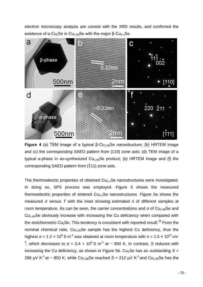
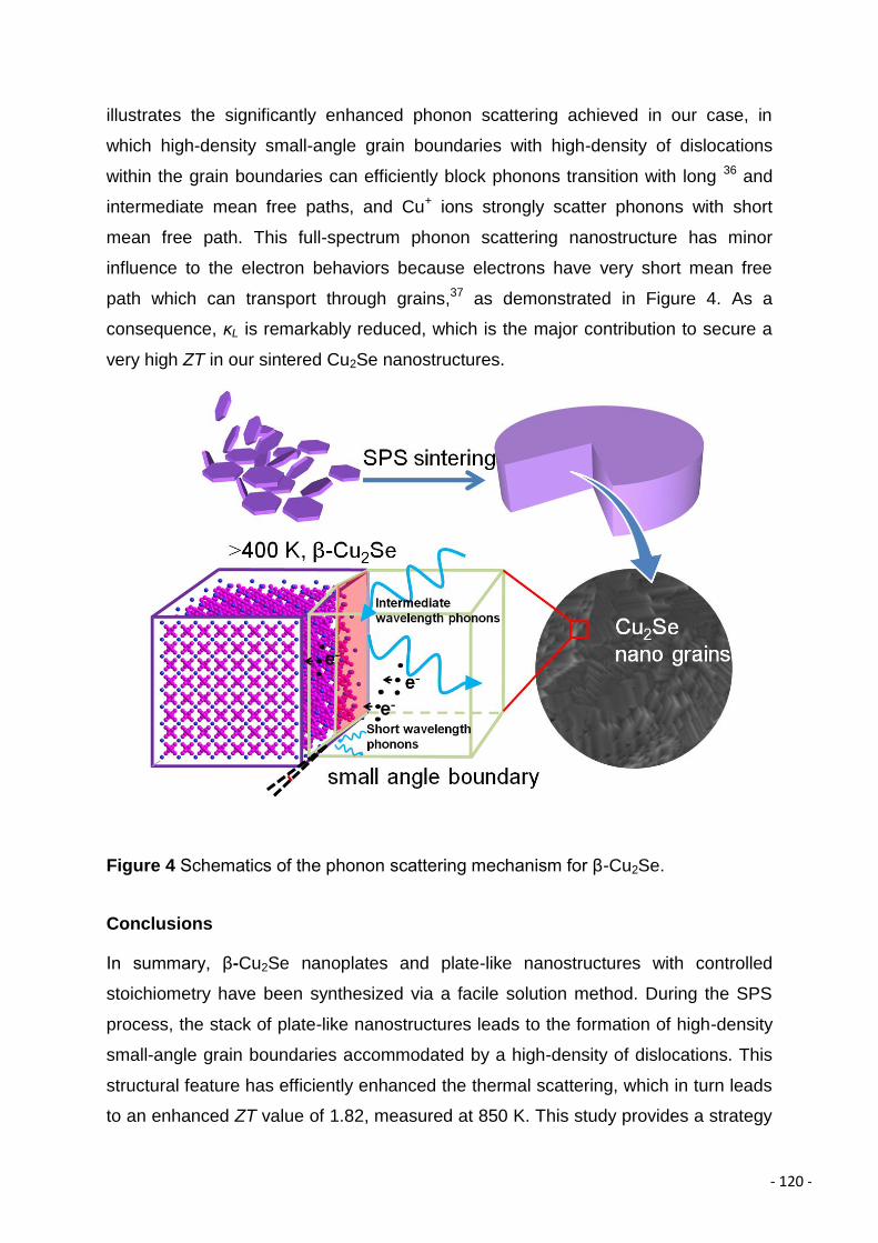
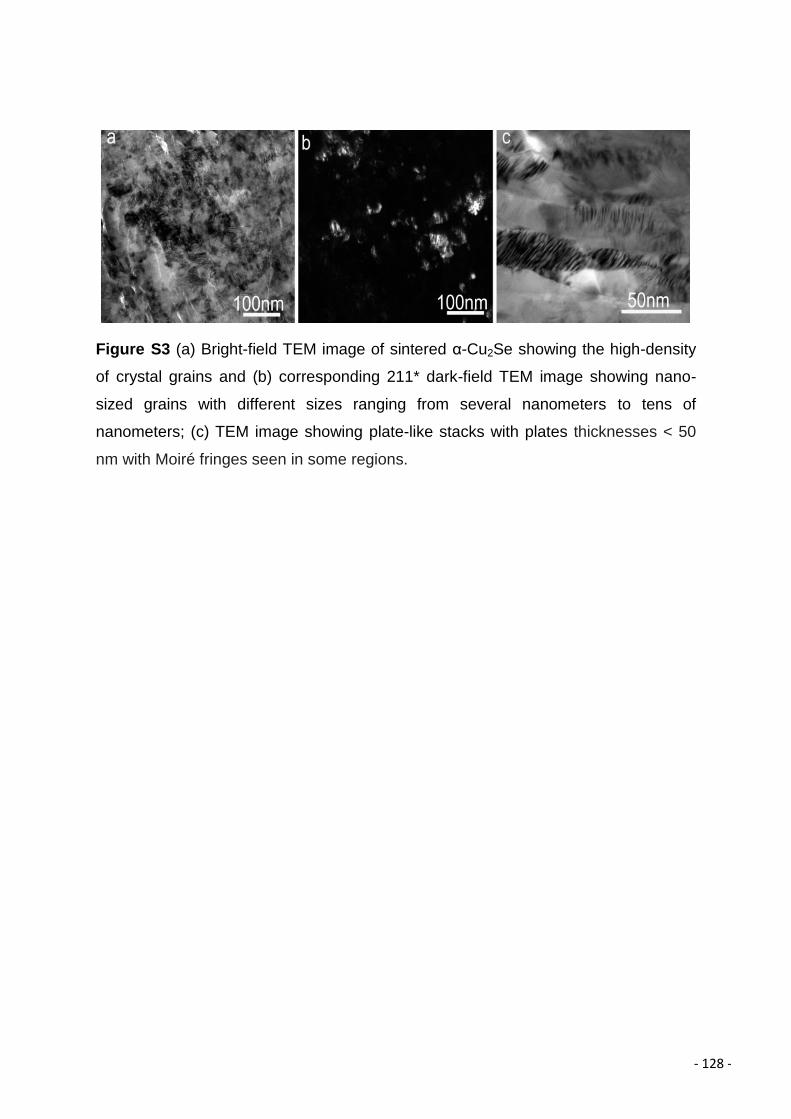
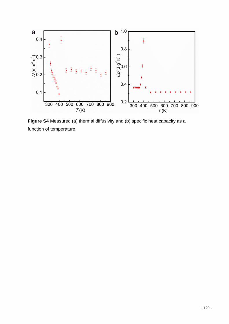
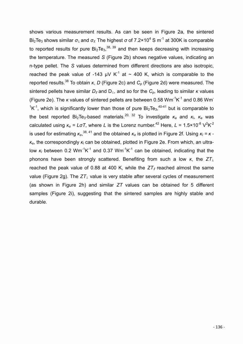
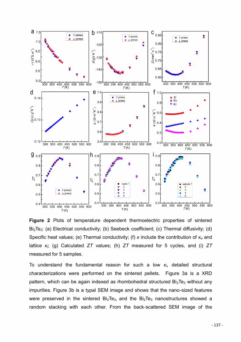
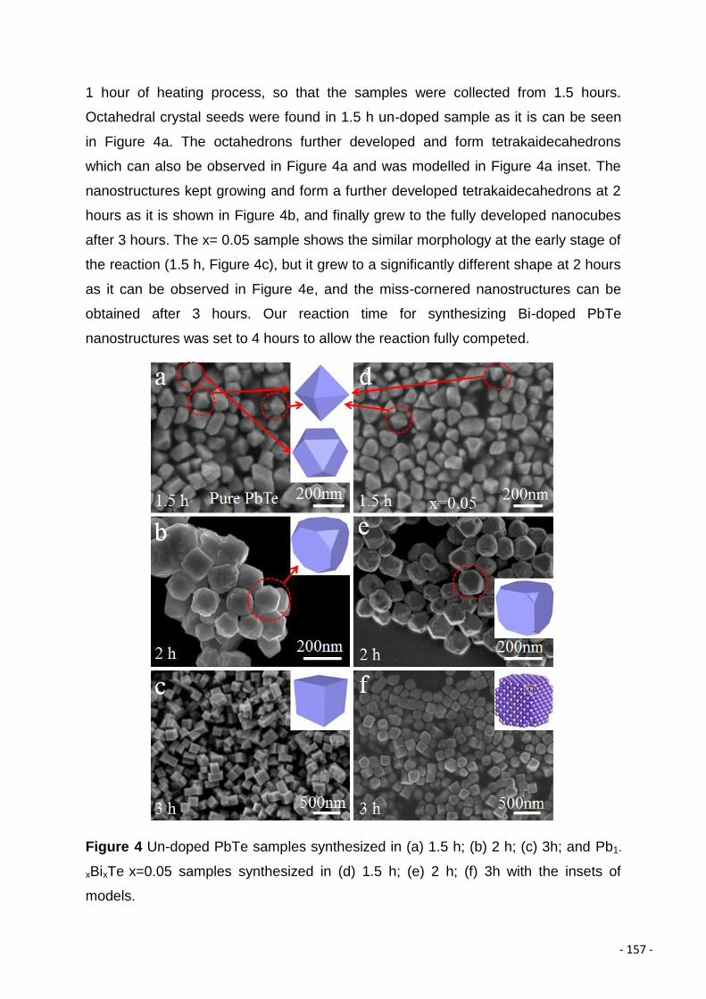
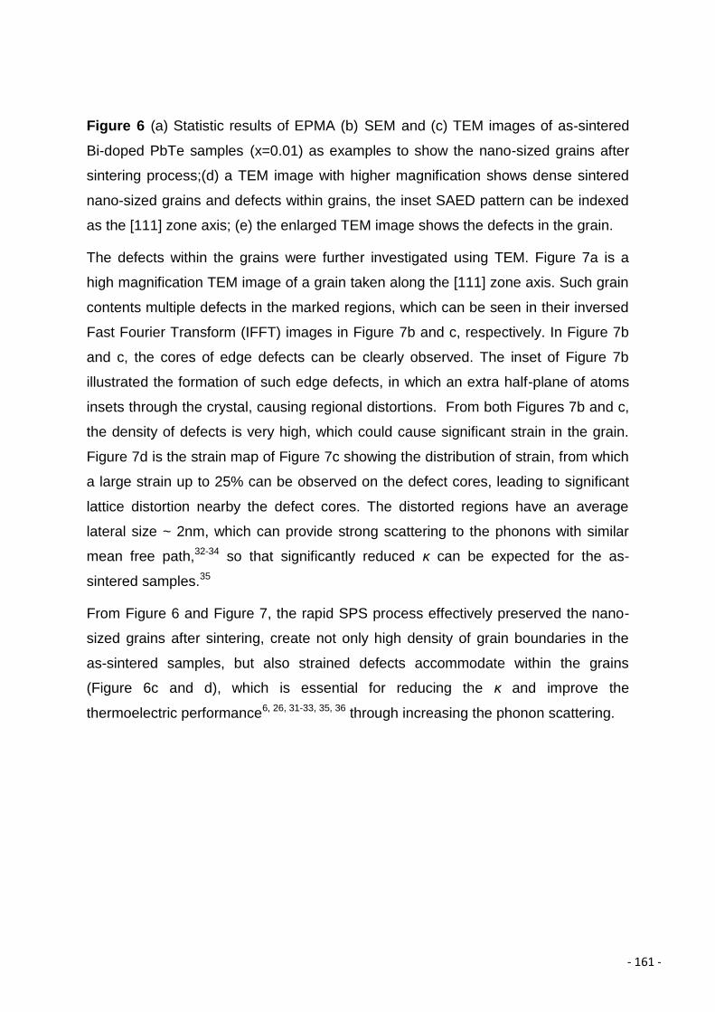
Page 1
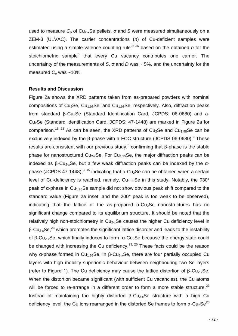
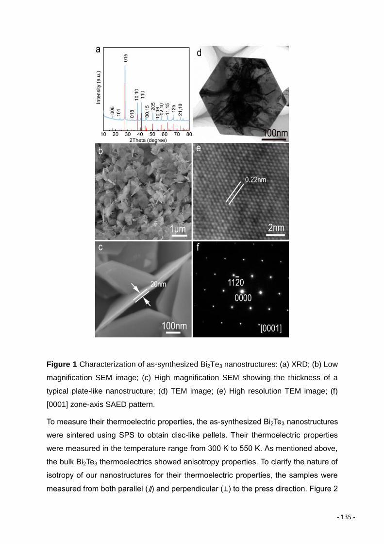
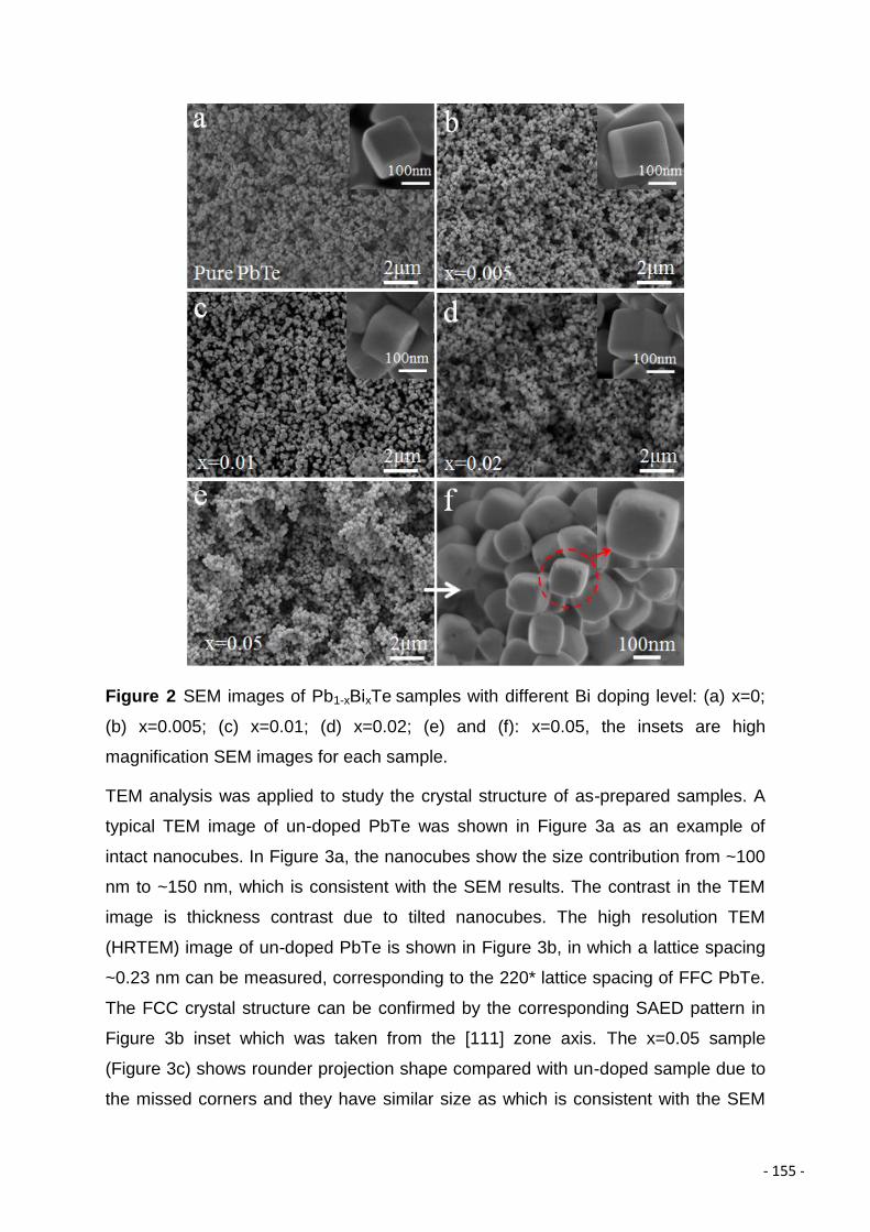
1
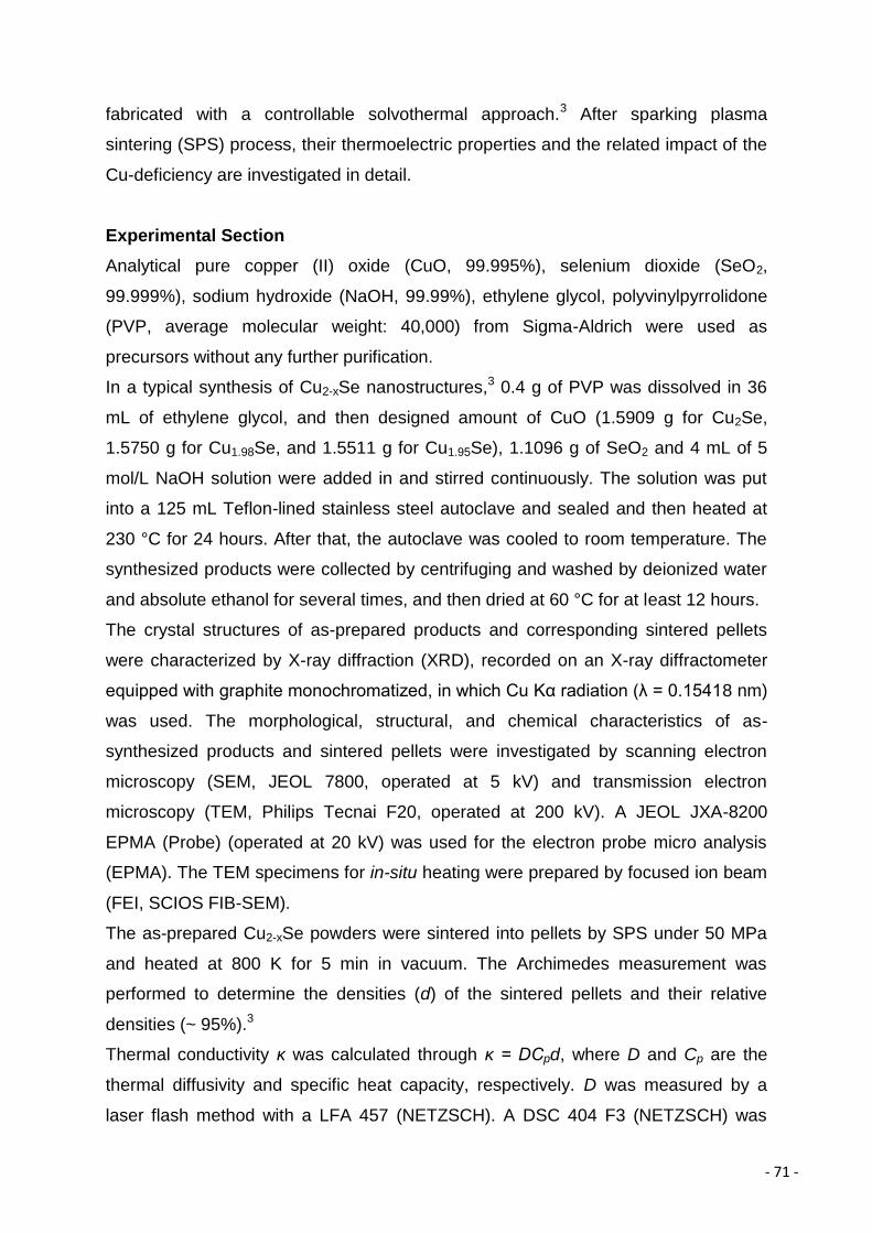
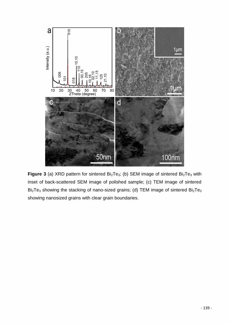
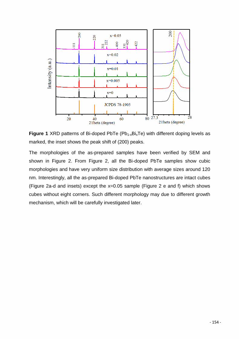
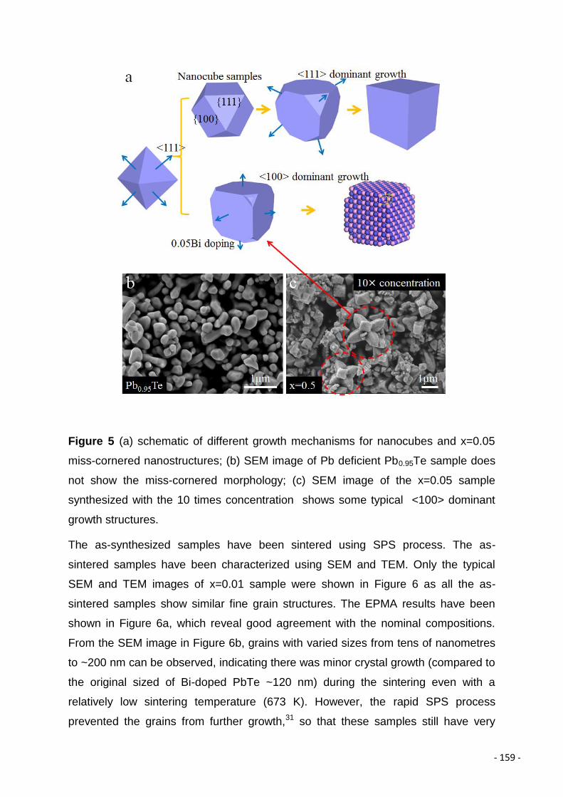
Development of High-efficiency Metal Chalcogenide
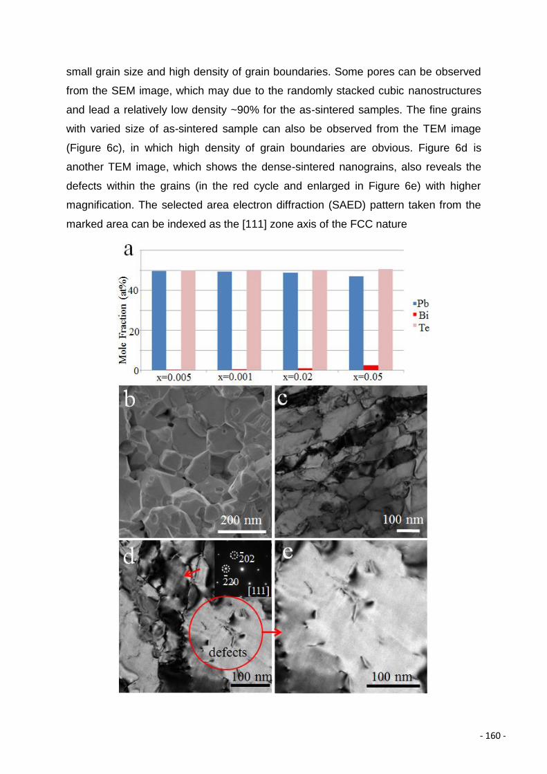
Thermoelectric Nanomaterials by Nanostructure Engineering
Lei Yang
Master of Philosophy in the Field of Nanotechnology
A thesis submitted for the degree of Doctor of Philosophy at
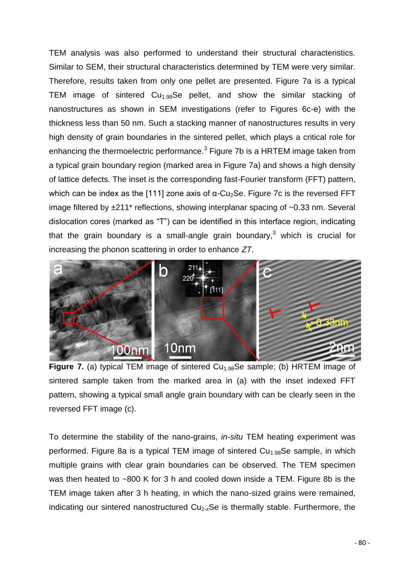
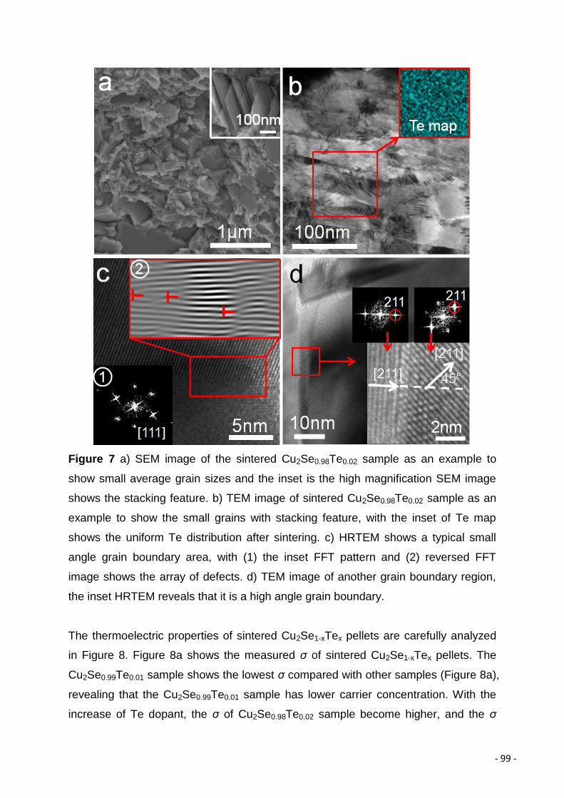
The University of Queensland in 2016
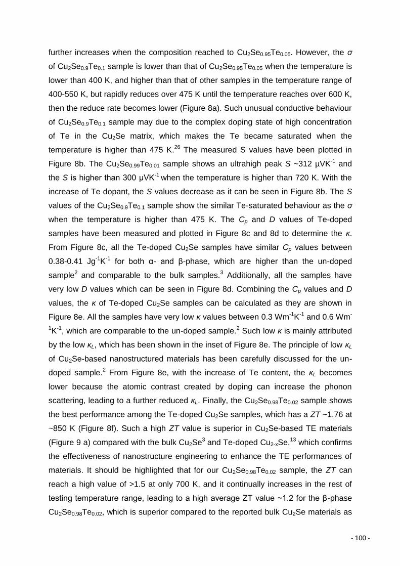
School of Mechanical and Mining Engineering
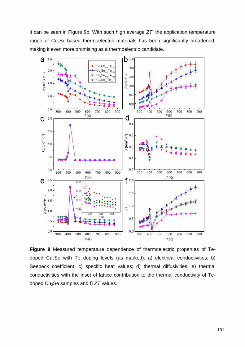
Page 2
2
Abstract
The development of high performance thermoelectric materials, which can
directly convert heat into electricity, is becoming an alternative to overcome
the global energy shortage. The efficiency of thermoelectric materials is
determined by the dimensionless figure-of-merit ZT=S2σT/κ, where S is the
Seebeck coefficient, σ is the electrical conductivity, T is the absolute
temperature, and κ is the thermal conductivity includes the contribution from
the electron (κe) and lattice (κL) components. High efficient thermoelectric
materials can be extensively applied as alternative energy sources in many
fields such as waste heat recycling, solid state power generation, and
refrigeration.
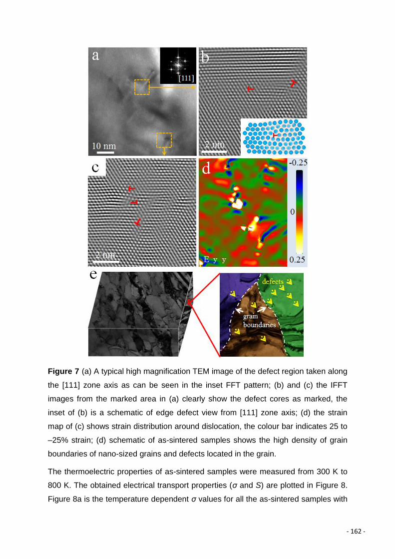
The challenge of developing high performance thermoelectric materials is how
to enhance the ZT value by optimizing the conflict and interdependent
parameters (S, σ and κ). Metal chalcogenides have been targeted in this
thesis because they intrinsically have good electrical transport properties
(high S and σ) and low κ. Among them, Bi2Te3, PbTe, and Cu2Se have the
highest ZT in room temperature, intermediate (500-800 K) and higher
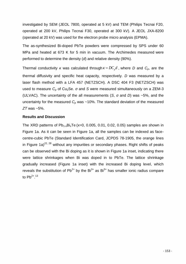
temperature (~1000 K) range, respectively. To further enhance their
thermoelectric performances, nanostructure engineering has been applied in
this thesis. Cu2Se, Bi2Te3 and PbTe nanomaterials have been synthesized via
facile and controllable solvothermal methods; their structures and
thermoelectric properties were extensively investigated.
Nanostructured β-phase Cu2Se materials were synthesized and sintered
using spark plasma sintering process. The nano-sized grains were preserved
after the sintering, leading to high density of small angle grain boundaries
accommodated by defects, which significantly reduced the κL of as-prepared
samples but did not affect the electrical transport properties, resulting an
outstanding ZT of 1.82 at around 850 K. Via a controlled synthesis approach,
Cu-deficient Cu2-xSe nanomaterials were obtained. The high degree of Cu
deficiency was found to trigger the phase transition from β- to α-phase,
leading to small amount of α-phase in the Cu1.95Se sample. The Cu deficiency
was proved to harm the thermoelectric performance of Cu2-xSe nanomaterials
via increasing the carrier concentration, and leading to a significantly reduced
Page 3
3
S. Tellurium was doped into Cu2Se nanomaterials to modify the electrical
transport properties. The effects of Te doping to the Cu2Se nanomaterials
were carefully studied, the Cu2Se0.99Te0.01 sample was found to have the
highest S among all the Te-doped samples and the ZT of Cu2Se0.98Te0.02 has
the highest peak ZT ~1.76.
The developed nanostructure engineering was approved to be effective on
Bi2Te3 and PbTe nanomaterials. Pure Bi2Te3 hexagonal nanoplates were
synthesized and sintered. High density of small angle grain boundaries
accommodated by defects were also found in the sintered Bi2Te3
nanomaterials, which significantly reduced the κ and resulted in an improved
ZT ~0.88 at 400 K. The Bi-doped PbTe nanocubes were obtained, and the
doping of Bi was confirmed via multiple technologies. The high density of
grain boundaries and the Bi dopant effectively reduced the κ. Also, the Bi
dopants improved the electrical transport properties of PbTe, finally leading to
enhanced ZT.
In this thesis, reliable, facile and controllable solvothermal methods were
developed to obtain metal chalcogenides-based nanomaterials. By applying
nanostructure engineering, the enhancement of thermoelectric performances
for metal chalcogenides-based nanomaterials has been achieved.
Page 4
4
Declaration by author
This thesis is composed of my original work, and contains no material
previously published or written by another person except where due reference
has been made in the text. I have clearly stated the contribution by others to
jointly-authored works that I have included in my thesis.
I have clearly stated the contribution of others to my thesis as a whole,
including statistical assistance, survey design, data analysis, significant
technical procedures, professional editorial advice, and any other original
research work used or reported in my thesis. The content of my thesis is the
result of work I have carried out since the commencement of my research
higher degree candidature and does not include a substantial part of work that
has been submitted to qualify for the award of any other degree or diploma in
any university or other tertiary institution. I have clearly stated which parts of
my thesis, if any, have been submitted to qualify for another award.
I acknowledge that an electronic copy of my thesis must be lodged with the
University Library and, subject to the policy and procedures of The University
of Queensland, the thesis be made available for research and study in
accordance with the Copyright Act 1968 unless a period of embargo has been
approved by the Dean of the Graduate School.
I acknowledge that copyright of all material contained in my thesis resides
with the copyright holder(s) of that material. Where appropriate I have
obtained copyright permission from the copyright holder to reproduce material
in this thesis.
Page 5
5
Publications during candidature
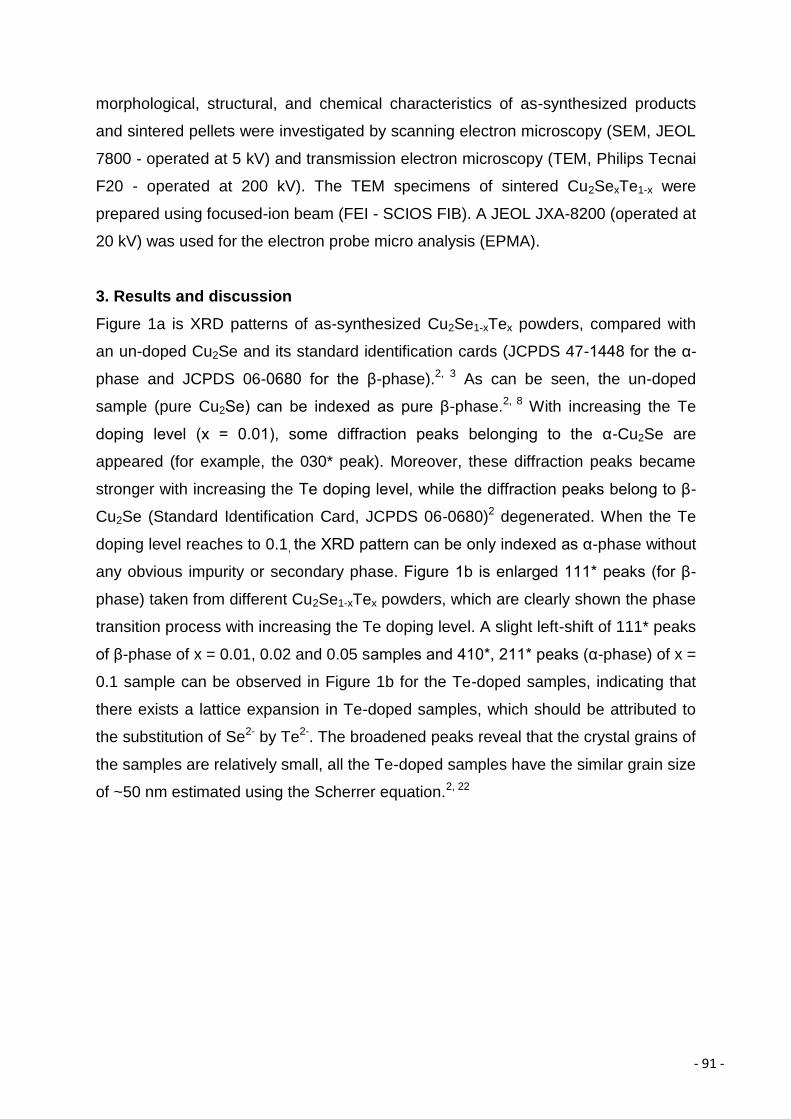
Peer-reviewed papers:
1. Yang, L.; Chen, Z. G.; Han, G.; Hong, M.; Huang, L.; Zou, J., Te-doped
Cu2Se nanoplates with high average thermoelectric figure of merit.
Journal of Materials Chemistry A, 2016, 4, 9213-9219.
2. Yang, L.; Chen, Z.-G.; Han, G.; Hong, M.; Zou, J., Impacts of Cu
deficiency on the thermoelectric properties of Cu2−XSe nanoplates.
Acta Materialia, 2016, 113, 140-146.
3. Yang, L.; Chen, Z.-G.; Nie, T.; Han, G.; Zhang, Z.; Hong, M.; Wang,
KL.; Zou, J., Co-doped Sb2Te3 Paramagnetic Nanoplates. Journal of
Materials Chemistry C, 2016, 4, 521-525.
4. Yang, L.; Chen, Z.-G.; Hong, M.; Han, G.; Zou, J., Enhanced
Thermoelectric Performance of Nanostructured Bi2Te3 through
Significant Phonon Scattering. ACS Applied Materials & Interfaces,
2015, 7, 23694-23699.
5. Yang, L.; Chen, Z.-G.; Han, G.; Hong, M.; Zou, Y.; Zou, J., High-
Performance Thermoelectric Cu2Se Nanoplates through Nanostructure
Engineering, Nano Energy, 2015, 16, 367-374.
6. Yang, L.; Chen, Z.-G.; Han, G.; Cheng, L.; Xu, H.; Zou, J., Trifold
Tellurium One-Dimensional Nanostructures and Their Formation
Mechanism. Crystal Growth & Design, 2013, 4796–4802.
7. Hong, M.; Chen, Z. G.; Yang, L.; Zou, J., Enhancing Thermoelectric
Performance of Bi2Te3-based Nanostructures through Rational
Structure Design. Nanoscale, 2016. DOI: 10.1039/C6NR00719H.
8. Hong, M.; Chen, Z. G.; Yang, L.; Zou, J., BixSb2−xTe3 nanoplates with
enhanced thermoelectric performance due to sufficiently decoupled
electronic transport properties and strong wide-frequency phonon
scatterings. Nano Energy, 2016, 20, 144-155.
9. Chen, Z.-G.; Zhang, C.; Zou, Y.; Zhang, E.; Yang, L.; Hong, M.; Xiu, F.;
Zou, J., Scalable Growth of High Mobility Dirac Semimetal Cd3As2
Microbelts. Nano Letters, 2015, 15, 5830−5834.
Page 6
6
10. Hong, M.; Chen, Z.-G.; Yang, L.; Han, G.; Zou, J., Enhanced
Thermoelectric Performance of Ultrathin Bi2Se3 Nanosheets through
Thickness Control. Advanced Electronic Materials, 2015, 1500025, 1-9.
11. Han, G.; Chen, Z.-G.; Ye, D.; Wang, B.; Yang, L.; Zou, Y.; Wang, L.;
Drennan, J.; Zou, J., In3Se4 and S-doped In3Se4 nano/micro-structures
as new anode materials for Li-ion batteries. The Journal of Materials
Chemistry A, 2015, 3, 7560–7567.
12. Chen, Z.-G.; Yang, L.; Ma, S.; Cheng, L.; Han, G.; Zhang, Z.-d.; Zou, J.,
Paramagnetic Cu-doped Bi2Te3 nanoplates. Applied Physics Letters,
2014, 104, 053105.
13. Han, G.; Chen, Z.-G.; Yang, L.; Hong, M.; Drennan, J.; Zou, J.,
Rational Design of Bi2Te3 Polycrystalline Whiskers for Thermoelectric
Applications. ACS Applied Materials & Interfaces, 2014, 7, 989-995.
14. Zou, Y.; Chen, Z.-G.; Huang, Y.; Yang, L.; Drennan, J.; Zou, J.,
Anisotropic Electrical Properties from Vapor–Solid–Solid Grown Bi2Se3
Nanoribbons and Nanowires. The Journal of Physical Chemistry C,
2014, 20620–20626.
15. Han, G.; Chen, Z. G.; Ye, D.; Yang, L.; Wang, L.; Drennan, J.; Zou, J.,
In-Doped Bi2Se3 Hierarchical Nanostructures as Anode Materials for Li-
Ion Batteries. The Journal of Materials Chemistry A, 2014, 7109-7116.
16. Liao, Z.-M.; Chen, Z.-G.; Lu, Z.-Y.; Xu, H.-Y.; Guo, Y.-N.; Sun, W.;
Zhang, Z.; Yang, L.; Chen, P.-P.; Lu, W.; Zou, J., Au impact on GaAs
epitaxial growth on GaAs (111)(B) substrates in molecular beam
epitaxy. Applied Physics Letters, 2013, 102 (6).
17. Han, G.; Chen, Z.-G.; Yang, L.; Cheng, L.; Jack, K.; Drennan, J.; Zou,
J., Thermal stability and oxidation of layer-structured rhombohedral
In3Se4 nanostructures. Applied Physics Letters, 2013, 103 (26).
18. Han, G.; Chen, Z.-G.; Yang, L.; Cheng, L.; Drennan, J.; Zou, J., Phase
Control and Formation Mechanism of New-Phase Layer-Structured
Rhombohedral In3Se4 Hierarchical Nanostructures. Crystal Growth &
Design, 2013, 5092–5099.
19. Han, G.; Chen, Z. G.; Sun, c.; Yang, L.; Cheng, L.; Li, Z.; Lu, W.; Gibbs,
Z. M.; Snyder, J.; Jack, K. S.; Drennan, J.; Zou, J., A New Crystal:
Page 7
7
Layer-Structured Rhombohedral In3Se4. Crystal Engineering
Communications, 2013, 393-398.
20. Cheng, L.; Chen, Z. G.; Yang, L.; Han, G.; Xu, H. Y.; Snyder, G. J.; Lu,
G. Q.; Zou, J., T-Shaped Bi2Te3–Te Heteronanojunctions: Epitaxial
Growth, Structural Modeling, and Thermoelectric Properties. The
Journal of Physical Chemistry C, 2013, 12458-12464.
21. Cheng, L.; Chen, Z. G.; Ma, S.; Zhang, Z. D.; Wang, Y.; Xu, H. Y.;
Yang, L.; Han, G.; Jack, K.; Lu, G. Q.; Zou, J., High Curie Temperature
Bi1.85Mn0.15Te3 Nanoplates. Journal of the American Chemical Society,
2012, 134 (46), 18920-18923.
22. Chen, Z. G.; Han, G.; Yang, L.; Cheng, L.; Zou, J., Nanostructured
thermoelectric materials: Current research and future challenge.
Progress in Natural Science: Materials International, 2012, 22 (6), 535-
549.
Conference Papers:
1. Liao, Z. M.; Xu, H. Y.; Sun, W.; Guo, Y. N.; Yang, L.; Chen, Z. G.;
Zou, J.; Lu, Z. Y.; Chen, P. P.; Lu, W., Effects of Au catalyst on GaAs
(111)B surface during annealing, on Optoelectronic and
Microelectronic Materials & Devices. COMMAD, 2012, 7-8.
Conference proceedings:
1. Yang, L., Chen, Z.G., Han, G., Cheng, L.N., Zou, j., Synthesis and
morphological modification of Te nanowires via a simple solvothermal
method. ACMM 22 / APMC 10 / ICONN 2012 Perth. 2012. (Oral
presentation)
2. Chen, Z.G., Yang, L., Han, G., Cheng, L.N., Zou, j., Development of
Thermoelectric Nanomaterials by a facile Solvothermal Method.
ACMM 22/ APMC 10 /ICONN 2012 Perth. 2012 (Oral presentation)
3. Han, G., Chen, Z.G., Yang, L., Cheng, L.N., Drennan, J., Zou, J., The
Solvothermal Synthesis of Indium Selenide Flowerlike Nanostructures.
ACMM 22/ APMC 10 /ICONN 2012 Perth. 2012. (Oral presentation)
4. Yang, L., Chen, Z.G., Han, G., Cheng, L.N., Zou, j., Understanding of
The Growth Mechanism of Tri-fold Tellurium Nanowires. UQ EAIT
Postgraduate Conference. Australia. 2012. (Oral presentation)
Page 8
8
5. Yang, L., Chen, Z.G., Han, G., Zou, j., Bi-doped PbTe Trifold
Nanostructures with improved thermoelectric performance. ICAMP8.
Gold Coast, Australia. 2014. (Oral presentation)
6. Yang, L., Chen, Z.G., Han, G., Zou, j., High-Performance
Thermoelectric Cu2Se Nanoplates through Nanostructure Engineering.
C-MRS. Guiyang, China. 2015. (Oral presentation)
7. Yang, L., Chen, Z.G., Zou, j., Nanostructure Engineering on Cu2Se-
based Thermoelectric Materials. The 35th International Conference &
The 1st Asian Conference on Thermoelectrics in Wuhan, China, 29th
May- 2nd June, 2016. (Oral presentation)
Page 9
9
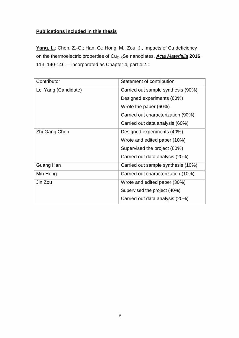
Publications included in this thesis
Yang, L.; Chen, Z.-G.; Han, G.; Hong, M.; Zou, J., Impacts of Cu deficiency
on the thermoelectric properties of Cu2−XSe nanoplates. Acta Materialia 2016,
113, 140-146. – incorporated as Chapter 4, part 4.2.1
Contributor Statement of contribution
Lei Yang (Candidate) Carried out sample synthesis (90%)
Designed experiments (60%)
Wrote the paper (60%)
Carried out characterization (90%)
Carried out data analysis (60%)
Zhi-Gang Chen Designed experiments (40%)
Wrote and edited paper (10%)
Supervised the project (60%)
Carried out data analysis (20%)
Guang Han Carried out sample synthesis (10%)
Min Hong Carried out characterization (10%)
Jin Zou Wrote and edited paper (30%)
Supervised the project (40%)
Carried out data analysis (20%)
Page 10
10
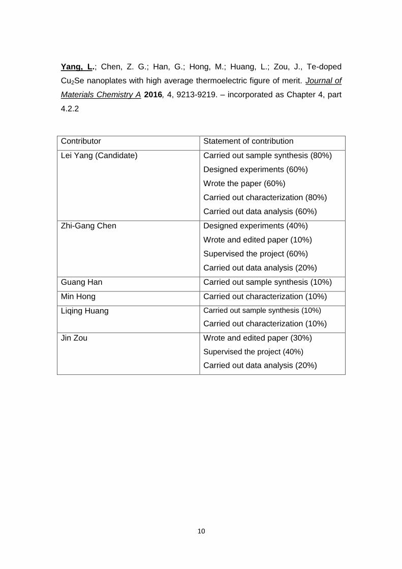
Yang, L.; Chen, Z. G.; Han, G.; Hong, M.; Huang, L.; Zou, J., Te-doped
Cu2Se nanoplates with high average thermoelectric figure of merit. Journal of
Materials Chemistry A 2016, 4, 9213-9219. – incorporated as Chapter 4, part
4.2.2
Contributor Statement of contribution
Lei Yang (Candidate) Carried out sample synthesis (80%)
Designed experiments (60%)
Wrote the paper (60%)
Carried out characterization (80%)
Carried out data analysis (60%)
Zhi-Gang Chen Designed experiments (40%)
Wrote and edited paper (10%)
Supervised the project (60%)
Carried out data analysis (20%)
Guang Han Carried out sample synthesis (10%)
Min Hong Carried out characterization (10%)
Liqing Huang Carried out sample synthesis (10%)
Carried out characterization (10%)
Jin Zou Wrote and edited paper (30%)
Supervised the project (40%)
Carried out data analysis (20%)
Page 11
11
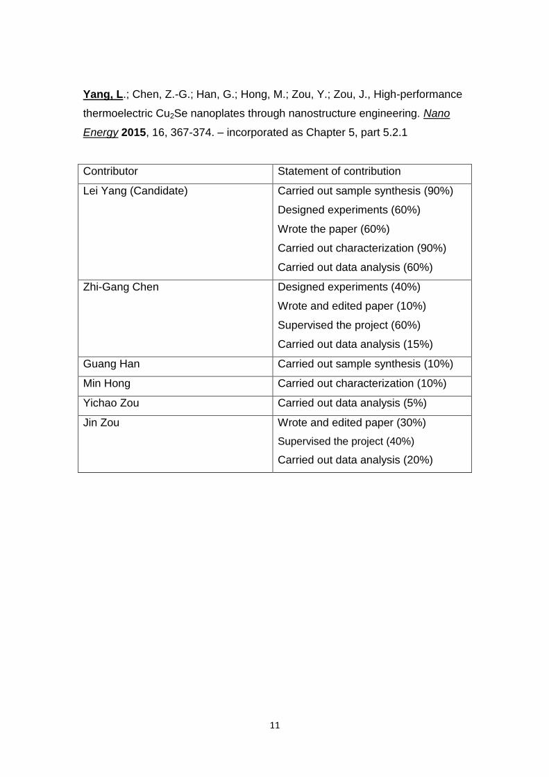
Yang, L.; Chen, Z.-G.; Han, G.; Hong, M.; Zou, Y.; Zou, J., High-performance
thermoelectric Cu2Se nanoplates through nanostructure engineering. Nano
Energy 2015, 16, 367-374. – incorporated as Chapter 5, part 5.2.1
Contributor Statement of contribution
Lei Yang (Candidate) Carried out sample synthesis (90%)
Designed experiments (60%)
Wrote the paper (60%)
Carried out characterization (90%)
Carried out data analysis (60%)
Zhi-Gang Chen Designed experiments (40%)
Wrote and edited paper (10%)
Supervised the project (60%)
Carried out data analysis (15%)
Guang Han Carried out sample synthesis (10%)
Min Hong Carried out characterization (10%)
Yichao Zou Carried out data analysis (5%)
Jin Zou Wrote and edited paper (30%)
Supervised the project (40%)
Carried out data analysis (20%)
Page 12
12
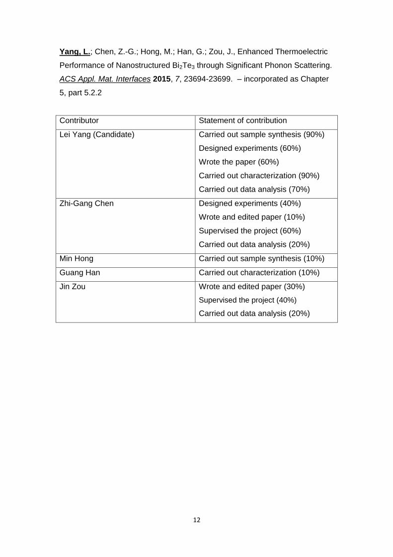
Yang, L.; Chen, Z.-G.; Hong, M.; Han, G.; Zou, J., Enhanced Thermoelectric
Performance of Nanostructured Bi2Te3 through Significant Phonon Scattering.
ACS Appl. Mat. Interfaces 2015, 7, 23694-23699. – incorporated as Chapter
5, part 5.2.2
Contributor Statement of contribution
Lei Yang (Candidate) Carried out sample synthesis (90%)
Designed experiments (60%)
Wrote the paper (60%)
Carried out characterization (90%)
Carried out data analysis (70%)
Zhi-Gang Chen Designed experiments (40%)
Wrote and edited paper (10%)
Supervised the project (60%)
Carried out data analysis (20%)
Min Hong Carried out sample synthesis (10%)
Guang Han Carried out characterization (10%)
Jin Zou Wrote and edited paper (30%)
Supervised the project (40%)
Carried out data analysis (20%)
Page 13
13
Contributions by others to the thesis
No contributions by others.
Statement of parts of the thesis submitted to qualify for the award of
another degree
None
Page 14
14
Acknowledgements
Firstly, I sincerely acknowledge my supervisors, Dr Zhi-Gang Chen and
Professor Jin Zou for their careful and kind guidance to me in every aspect of
my PhD study in the University of Queensland. I admire their impressing
excellence as scientific researchers: well-rounded and profound knowledge,
determination, great patience, passion and the seriousness. They devote
themselves to pursue and share the scientific truth, also help many students
like me to develop the experimental skills and the ability to accomplish
scientific research projects. They have spent huge effort to teach me how to
design experiments and write scientific papers. It is a great honour for me to
join this family-like group under their supervisions.
Also, I would like to thank my colleagues, Dr Yong Wang, Mrs Ya Wang, Dr
Yang Huang, Dr Jing Lin, Dr Yanan Guo, Dr Lina Cheng, Dr Hongyi (Justin)
Xu, Dr Guang Han, Dr Wen Sun, Dr Zhi Zhang, Dr Kun Zheng, Dr Lihua
Wang, Zhiming Liao, Min Hong, Yichao Zou, Mun Soo, Chen Zhou, Liqing
Huang, in our research group at The University of Queensland. Thank you
very much for sharing your knowledge and skills, providing great help and
support in both of my study and life in Brisbane.
I acknowledge all the staff of Centre for Microscopy and Microanalysis (CMM)
at the University of Queensland for their technical support. I have learned
many useful analysing skills from them. And I acknowledge the financial
support from the China Scholarship Council for providing my PhD stipend.
Last but not least, I want to give my great thanks to my family: my dad, my
mum, and my elder sister, my wife Zilin Zhang, and all my friends in China
and Australia. Their endless love and encouragement are always the great
power in my life.
Page 15
15
Keywords
Thermoelectric materials, high performance, metal chalcogenides,
nanostructure engineering, solvothermal synthesis.
Australian and New Zealand Standard Research Classifications
(ANZSRC)
ANZSRC code: 091205, Functional Materials, 50%
ANZSRC code: 100706, Nanofabrication, Growth and Self Assembly, 40%
ANZSRC code: 100712, Nanoscale Characterisation, 10%
Fields of Research (FoR) Classification
FoR code: 0912, Materials Engineering, 50%
FoR code: 1007, Nanotechnology, 50%
Page 17
i
Table of Contents Chapter 1: Introduction ........................................................................................... - 1 -
1.1 Background .................................................................................................... - 1 -
1.2 Objective and Scopes ..................................................................................... - 3 -
1.3 Thesis outline ................................................................................................. - 4 -
Chapter 2: Literature Review .................................................................................. - 6 -
2.1 Thermoelectric Effects .................................................................................... - 6 -
2.1.1 Seebeck Effect........................................................................................ - 7 -
2.1.2 Peltier Effect ........................................................................................... - 7 -
2.1.3 Thomson Effect....................................................................................... - 7 -
2.1.4 Thermoelectric Generation and Refrigeration and the Figure-of-Merit .... - 8 -
2.1.5 Effective Factors ................................................................................... - 10 -
2.2 Development of Thermoelectric Materials .............................................. - 12 -
2.2.1 Thermoelectric Alloys ........................................................................... - 13 -
2.2.2 Materials of Complex Structures ........................................................... - 14 -
2.2.3 Metal Chalcogenides Thermoelectric Materials .................................... - 15 -
2.3 Principles and Methodologies to Achieve High ZT ....................................... - 26 -
2.3.1 Optimize the Carrier Concentration ...................................................... - 26 -
2.3.2 Band Engineering ................................................................................. - 28 -
2.3.3 Nanostructure Engineering ................................................................... - 30 -
2.4 Unsolved Issues and Opportunities .............................................................. - 33 -
2.5 Summary ...................................................................................................... - 34 -
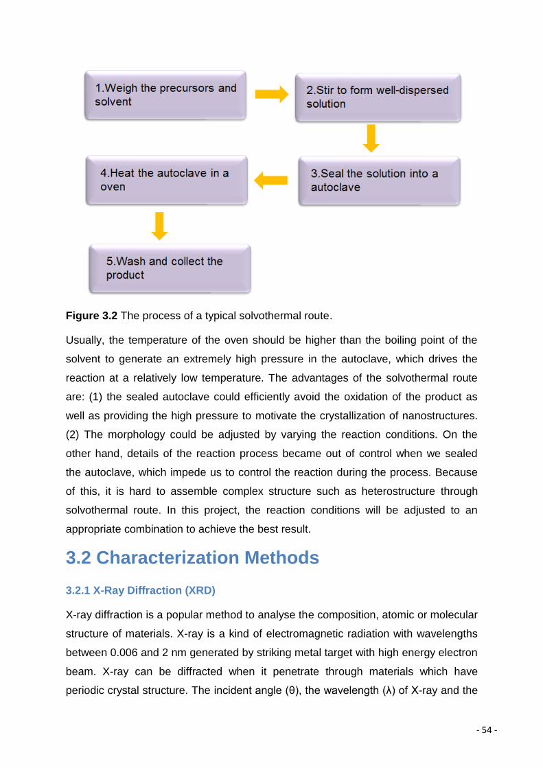
Chapter 3 Methodologies ........................................................................................................ - 51 -
3.1 Synthesis Methods ....................................................................................... - 51 -
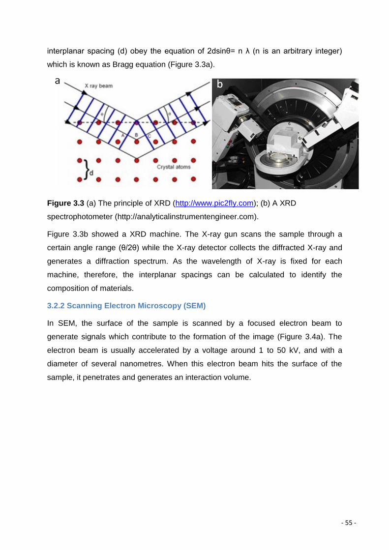
3.2 Characterization Methods ............................................................................. - 54 -
3.2.1 X-Ray Diffraction (XRD) ........................................................................ - 54 -
3.2.2 Scanning Electron Microscopy (SEM) .................................................. - 55 -
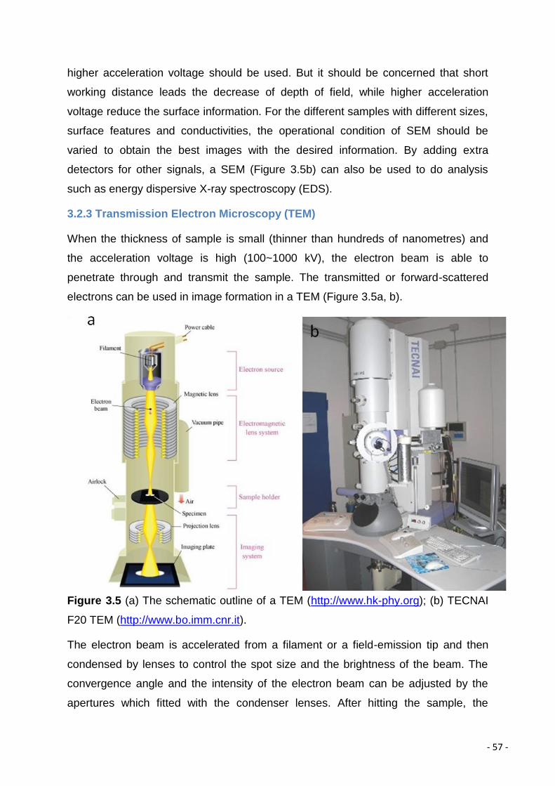
3.2.3 Transmission Electron Microscopy (TEM) ............................................ - 57 -
3.3 Thermoelectric Measurements ..................................................................... - 59 -
3.3.1 Thermal Properties ............................................................................... - 59 -
3.3.2 Seebeck Coefficient .............................................................................. - 60 -
3.3.3 Electrical properties .............................................................................. - 61 -
Page 18
ii
Chapter 4 Controllable Synthesis of Metal Chalcogenides Nanostructures and Their
Thermoelectric Performances ........................................................................... - 66 -
4.1 Introduction ................................................................................................... - 66 -
4.2 Manuscripts for Publication........................................................................... - 66 -
4.2.1 Effects of Cu Deficiency on the Thermoelectric Properties of Cu2-XSe
Nanostructures .............................................................................................. - 67 -
4.2.2 Te-induced Phase Transition of Cu2SexTe1-x Nanomaterials and Their
Thermoelectric Properties .............................................................................. - 87 -
Chapter 5 Enhanced Thermoelectric Performances of Metal Chalcogenides via
Nanostructure Engineering ................................................................ - 107 -
5.1 Introduction ................................................................................................. - 107 -
5.2 Journal Publications and Manuscript .......................................................... - 107 -
5.2.1 High-Performance Thermoelectric Cu 2Se Nanoplates through
Nanostructure Engineering .......................................................................... - 108 -
5.2.2 Enhanced Thermoelectric Performance of Nanostructured Bi2Te3 through
Significant Phonon Scattering ...................................................................... - 130 -
5.2.3 Manuscript .......................................................................................... - 149 -
Chapter 6 Conclusions and Recommendations ................................................. - 171 -
Page 19
- 1 -
List of Figures
Figure 1.1 Global energy supply (http://aleklett.wordpress.com).
Figure 1.2 ZT values of different materials as a function of temperature.
Figure 2.1 (a) Schematic diagram shows the thermoelectric process; (b) typical
thermoelectric module.
Figure 2.2 Efficiency of thermoelectric devices as a function of ΔT.
Figure 2.3 The relation between carrier concentration and the value of ZT.
Figure 2.4 Figure of merit (ZT) as a function of temperature for several high-
efficiency bulk thermoelectric materials
(http://chemgroups.northwestern.edu/kanatzidis/greatthermo.html).
Figure 2.5.(a-c) Crystal structure of CoSb3 revealing the large voids with rattlers, the
type-I clathrate Na8Si46, and β-Zn4Sb3; (d) ZT as a function of temperature for
skutterudites as thermoelectric materials; (e) Variable temperature ZT of clathrates,
and β-Zn4Sb3.
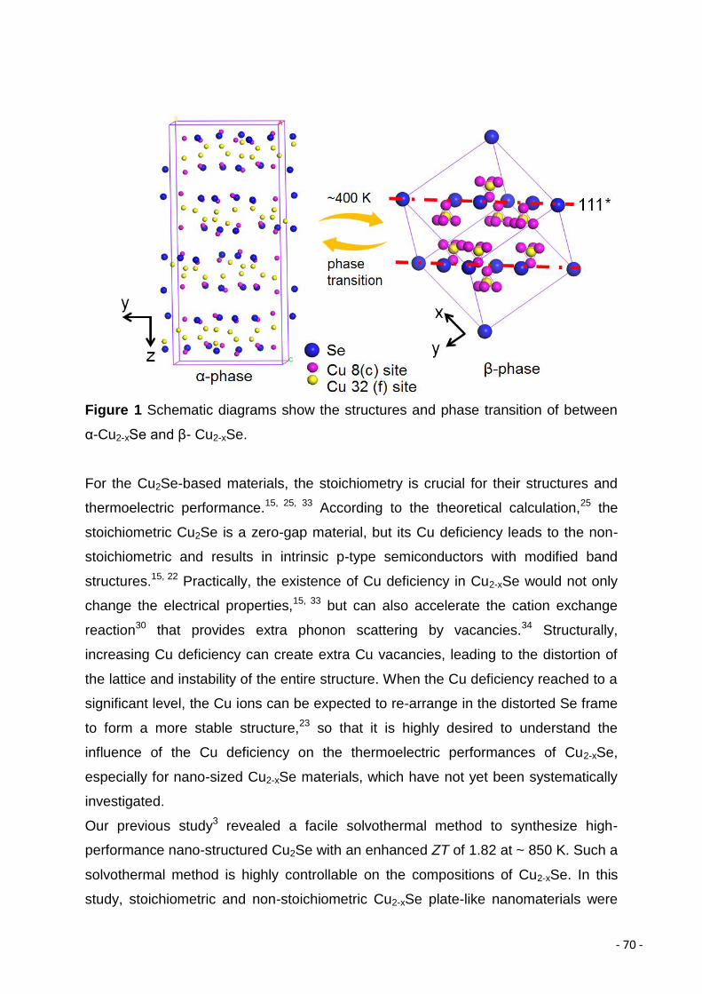
Figure 2.6 Schematics shows the structures and phase transition of Cu2-xSe
between α- and β-phase.
Figure 2.7 Rhombohedral crystal structure of Bi2Te3.
Figure 2.8 Valence band structure of PbTe1-xSex. (a) Brillouin zone showing the low
degeneracy hole pockets (orange) centred at the L point, and the high degeneracy
hole pockets (blue) along the Σ line. (b) Relative energy of the valence bands in
PbTe0.85Se0.15. At 500K the two valence bands converge, resulting in transport
contributions from both the L and Σ bands.
Figure 2.9 (a), (b) Experimental power factors as a function of Hall carrier
concentration; (c), (d) calculated power factors as a function of Hall carrier
concentration and (e), (f) calculated power factors as a function of reduced Fermi
level for Pb1-xLaxTe and PbIxTe1-x, respectively.
Figure 2.10 Schematic illustrates the resonant level on the electronic density of
states (DOS).
Figure 2.11 Schematic diagram of phonon scattering mechaism and electronic
transport within a thermalelectric material.
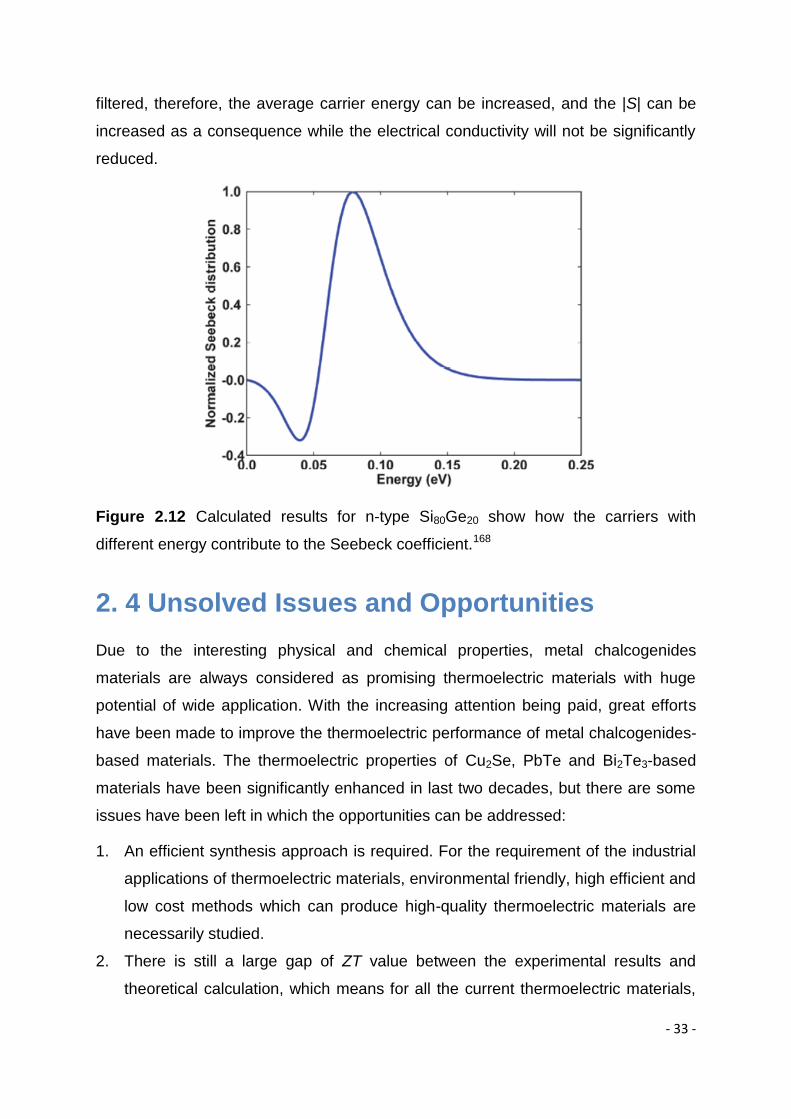
Figure 2.12 Calculated results for n-type Si80Ge20 show how the carriers with
different energy contribute to the Seebeck coefficient.
Page 20
- 2 -
Figure 3.1 An autoclave used in solvothermal synthesis.
Figure 3.2 The process of a typical solvothermal route.
Figure 3.3 (a) The principle of XRD (http://www.pic2fly.com); (b) A XRD
spectrophotometer (http://analyticalinstrumentengineer.com).
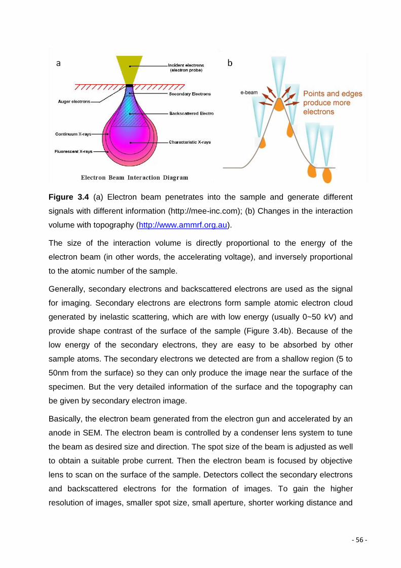
Figure 3.4 (a) Electron beam penetrates into the sample and generate different
signals with different information (http://mee-inc.com); (b) Changes in the interaction
volume with topography (http://www.ammrf.org.au).
Figure 3.5 (a) The schematic outline of a TEM (http://www.hk-phy.org); (b) TECNAI
F20 TEM (http://www.bo.imm.cnr.it).
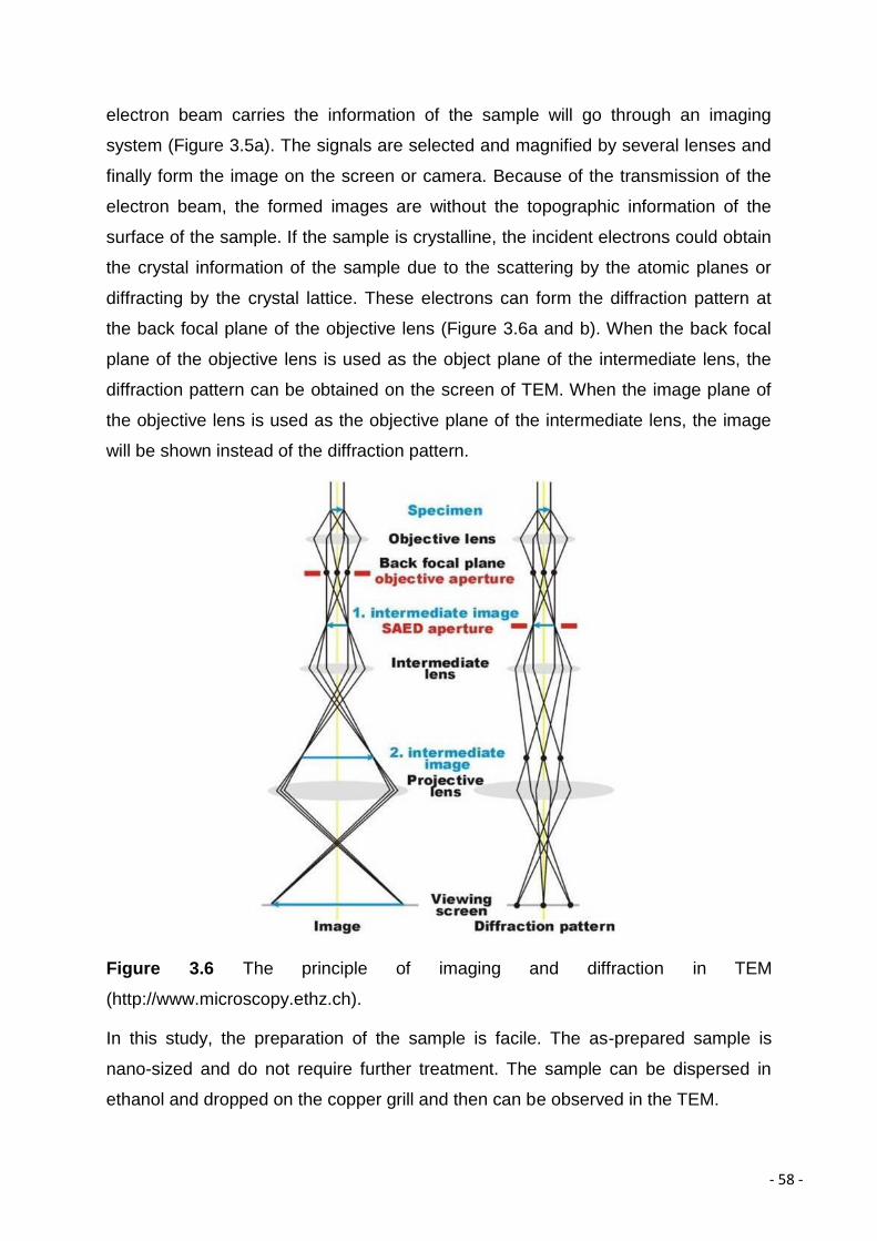
Figure 3.6 The principle of imaging and diffraction in TEM
(http://www.microscopy.ethz.ch).
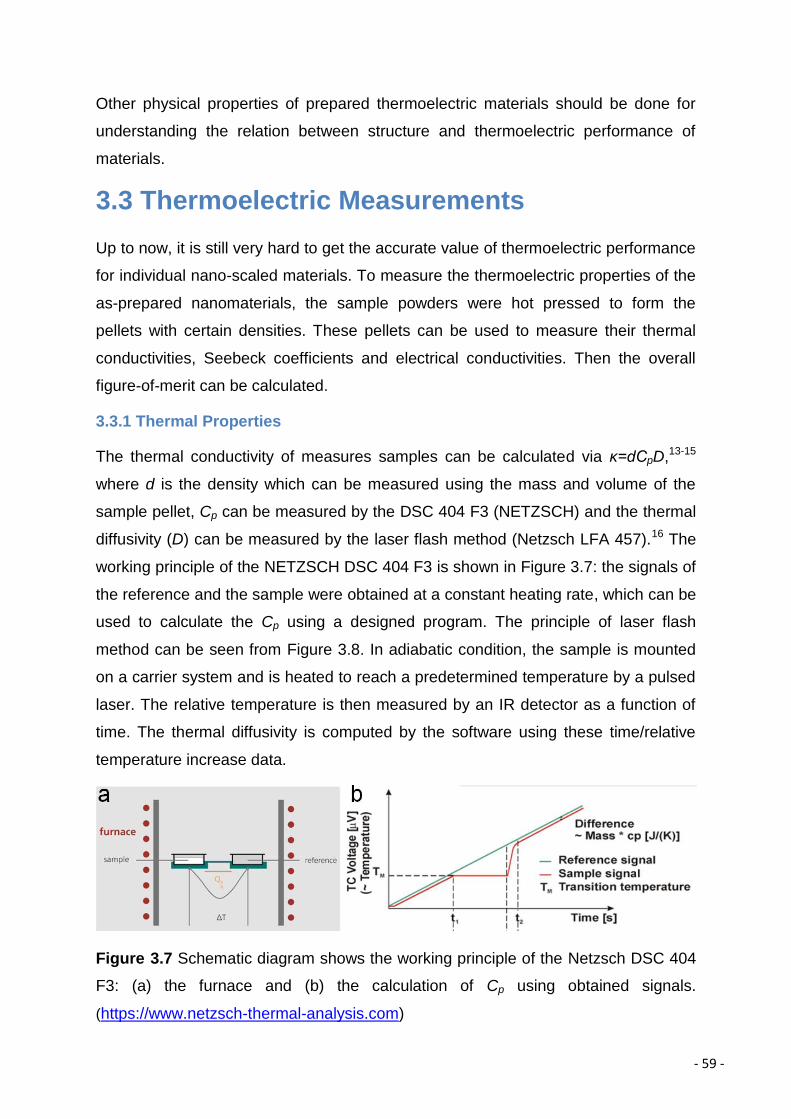
Figure 3.7 Schematic diagram shows the working principle of the Netzsch DSC 404
F3: (a) the furnace and (b) the calculation of Cp using obtained signals.
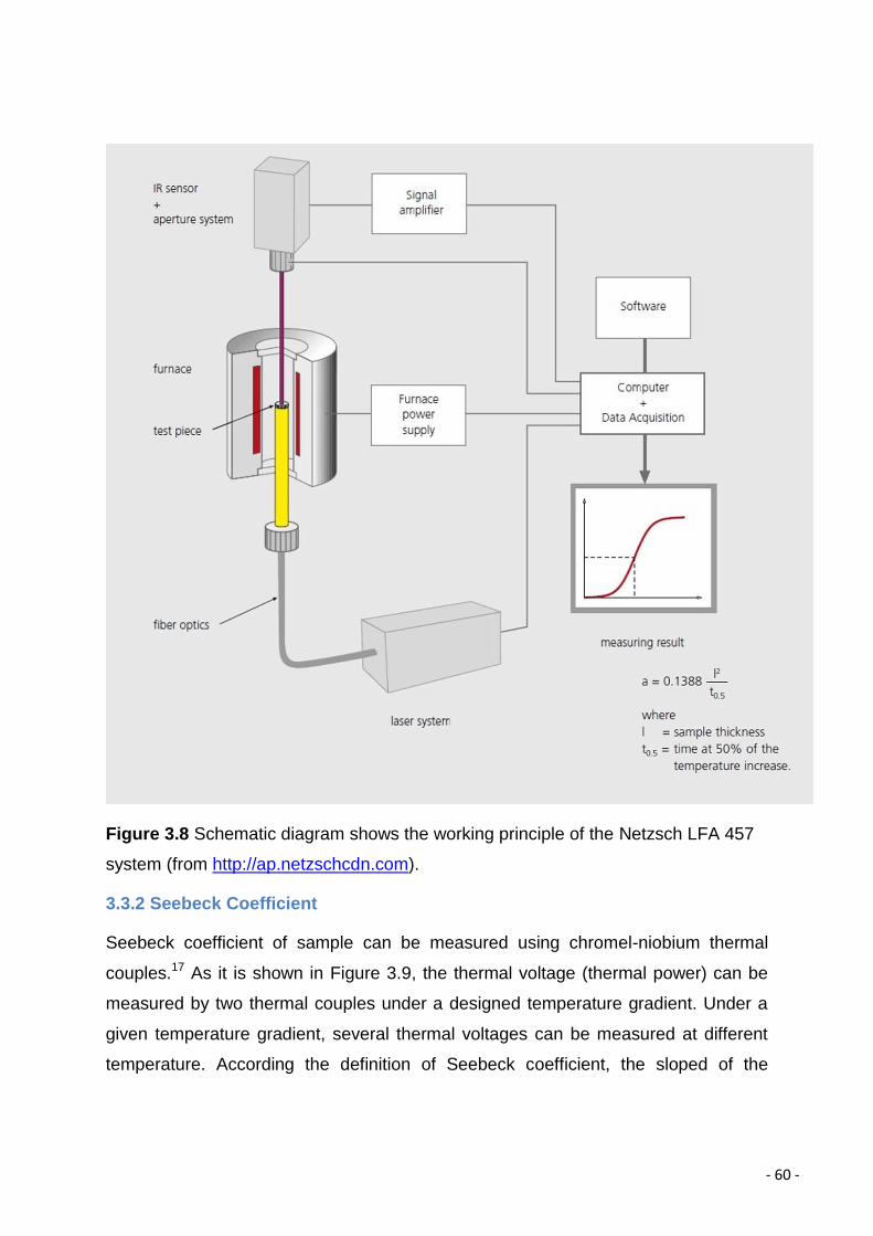
Figure 3.8 Schematic diagram shows the working principle of the Netzsch LFA 457
system (from http://ap.netzschcdn.com).
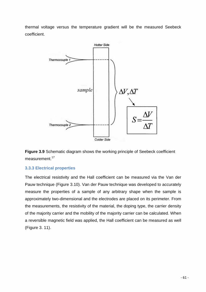
Figure 3.9 Schematic diagram shows the working principle of Seebeck coefficient
measurement.
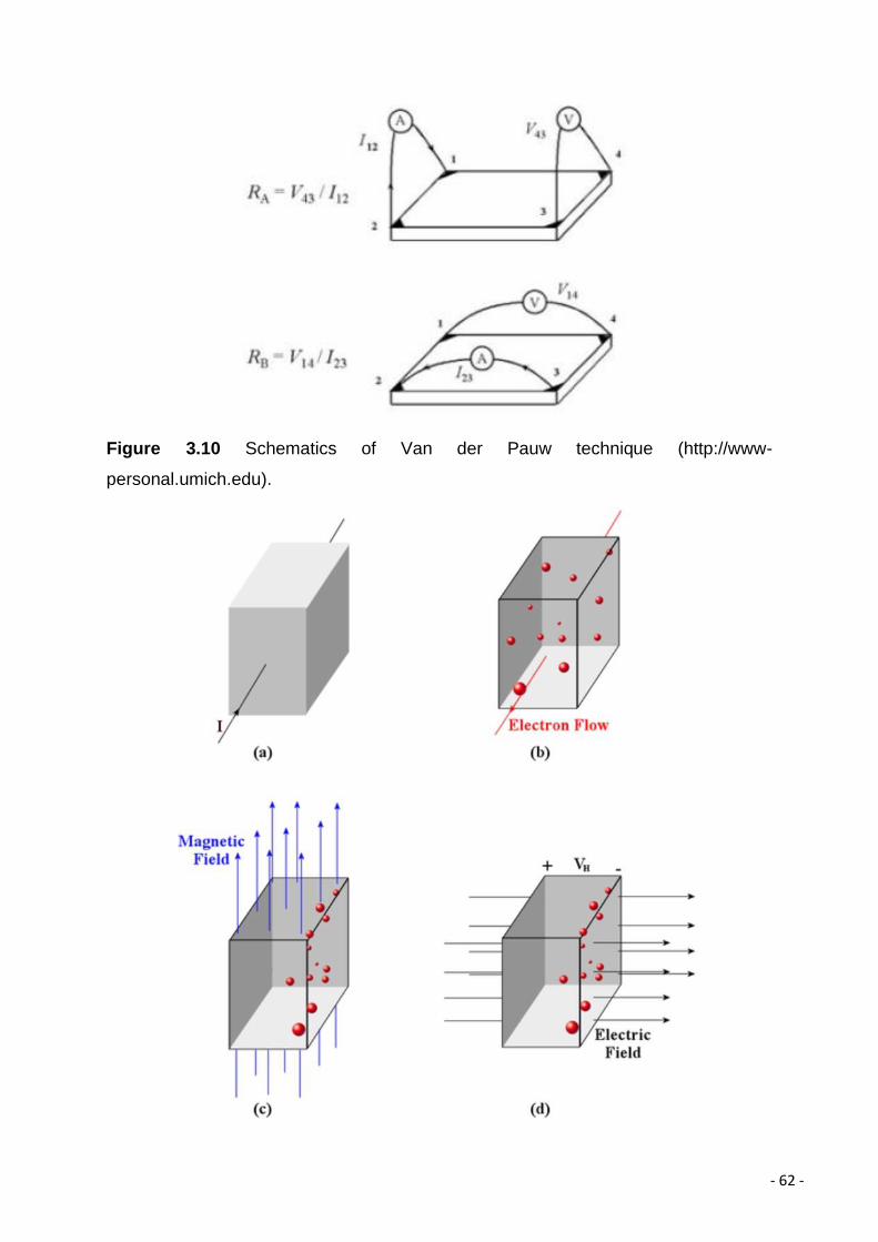
Figure 3.10 Schematics of Van der Pauw technique (http://www-
personal.umich.edu).
Figure 3.11 The measurement of Hall coefficient using Van der Pauw technique
under a reversible magnetic field
(http://en.wikipedia.org/wiki/File:Van_der_Pauw_Method_-_Hall_Effect.png).
Page 21
- 3 -
List of Tables
Table 1 Thermoelectric properties of advanced Bi2Te3-based materials
Table 2 Advanced thermoelectric materials in Pb-Te system
Table 3 Common synthesis methods of low dimensional materials
Page 22
- 4 -
List of Abbreviations RTGs: radioisotope thermoelectric generators
PGEC: phonon-glass/electron-crystal
FCC: face-center-cubic
COP: coefficient of performance
MS: melt spinning
HP: hot pressing
HEBM: high energy ball milling
SPS: spark plasma sintering
SP: solution phase method
MW: microwave synthesis
CC: cold compaction
NASA: the national aeronautics and space administration
MBE: molecular beam epitaxy
CVD: chemical vapour deposition
XRD: X-ray diffraction
SEM: scanning electron microscope
TEM: transmission electron microscope
EDS: energy dispersive X-ray spectroscopy
JCPDS: the joint committee on powder diffraction standards
HRTEM: high-resolution TEM
SAED: selected area electron diffraction
FFT: fast Fourier transform
EPMA: electron probe micro analysis
FIB: focused ion beam
XPS: X-ray photoelectron spectroscopy
Page 23
- 1 -
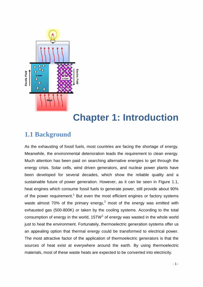
Chapter 1: Introduction
1.1 Background
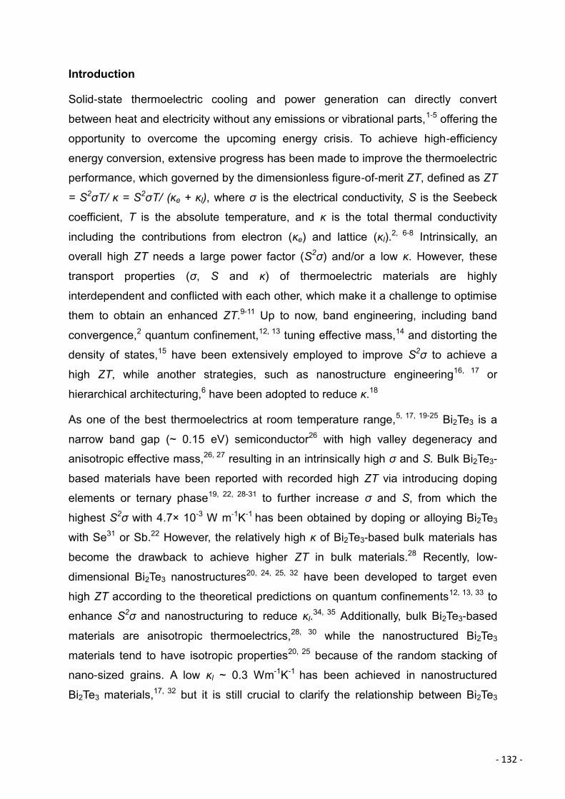
As the exhausting of fossil fuels, most countries are facing the shortage of energy.
Meanwhile, the environmental deterioration leads the requirement to clean energy.
Much attention has been paid on searching alternative energies to get through the
energy crisis. Solar cells, wind driven generators, and nuclear power plants have
been developed for several decades, which show the reliable quality and a
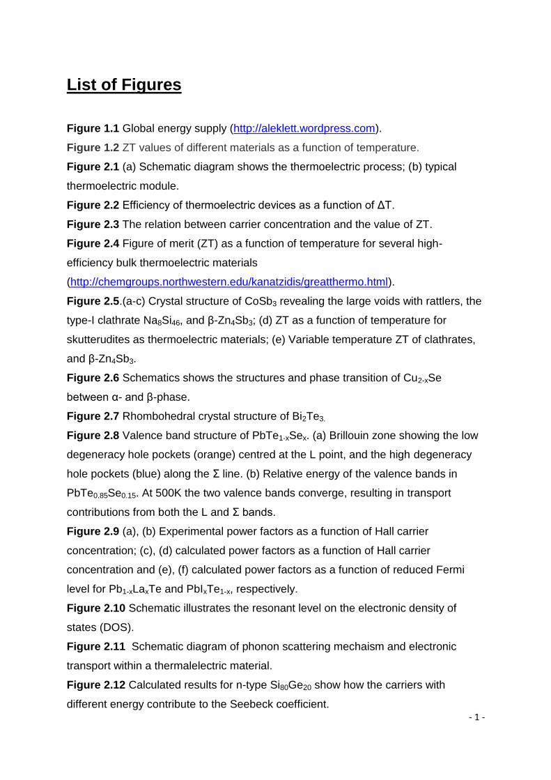
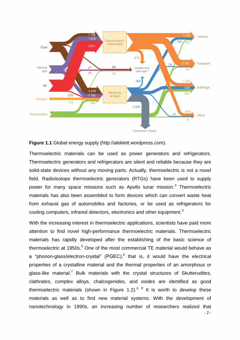
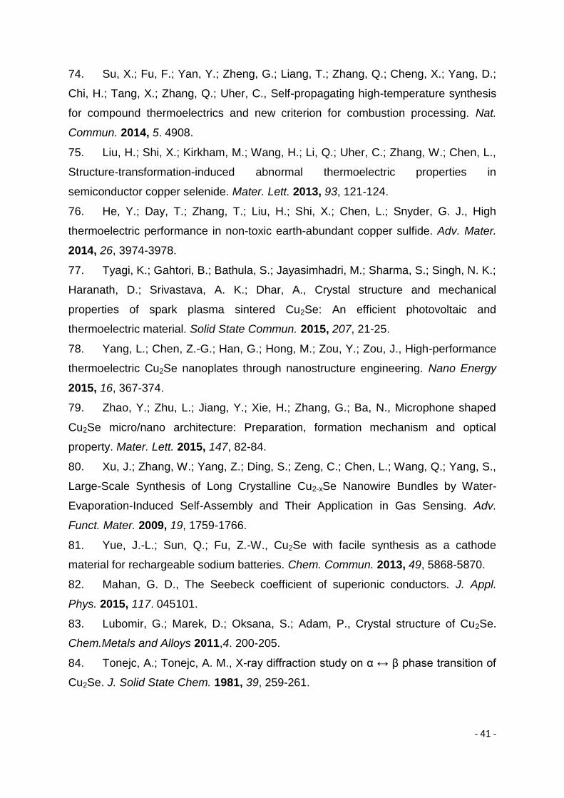
sustainable future of power generation. However, as it can be seen in Figure 1.1,
heat engines which consume fossil fuels to generate power, still provide about 90%
of the power requirement.1 But even the most efficient engines or factory systems
waste almost 70% of the primary energy,2 most of the energy was emitted with
exhausted gas (500-800K) or taken by the cooling systems. According to the total
consumption of energy in the world, 15TW1 of energy was wasted in the whole world
just to heat the environment. Fortunately, thermoelectric generation systems offer us
an appealing option that thermal energy could be transformed to electrical power.
The most attractive factor of the application of thermoelectric generators is that the
sources of heat exist at everywhere around the earth. By using thermoelectric
materials, most of these waste heats are expected to be converted into electricity.
Page 24
- 2 -
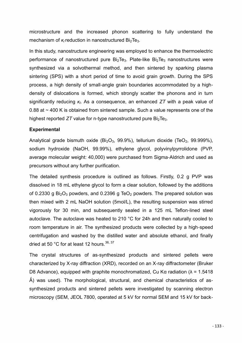
Figure 1.1 Global energy supply (http://aleklett.wordpress.com).
Thermoelectric materials can be used as power generators and refrigerators.
Thermoelectric generators and refrigerators are silent and reliable because they are
solid-state devices without any moving parts. Actually, thermoelectric is not a novel
field. Radioisotope thermoelectric generators (RTGs) have been used to supply
power for many space missions such as Apollo lunar mission.3 Thermoelectric
materials has also been assembled to form devices which can convert waste heat
from exhaust gas of automobiles and factories, or be used as refrigerators for
cooling computers, infrared detectors, electronics and other equipment.4
With the increasing interest in thermoelectric applications, scientists have paid more
attention to find novel high-performance thermoelectric materials. Thermoelectric
materials has rapidly developed after the establishing of the basic science of
thermoelectric at 1950s.5 One of the most commercial TE material would behave as
a “phonon-glass/electron-crystal” (PGEC),6 that is, it would have the electrical
properties of a crystalline material and the thermal properties of an amorphous or
glass-like material.7 Bulk materials with the crystal structures of Skutterudites,
clathrates, complex alloys, chalcogenides, and oxides are identified as good
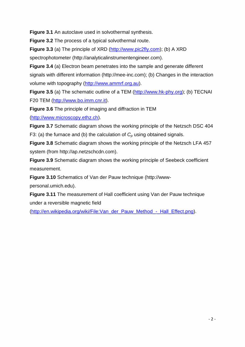
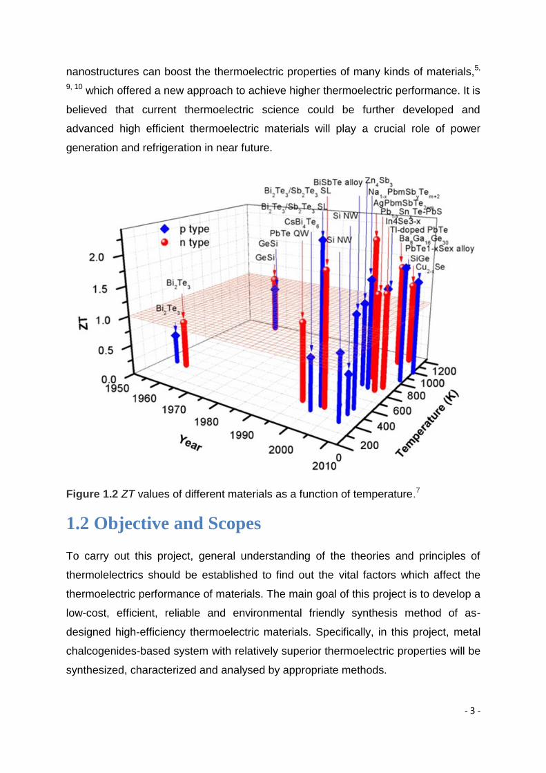
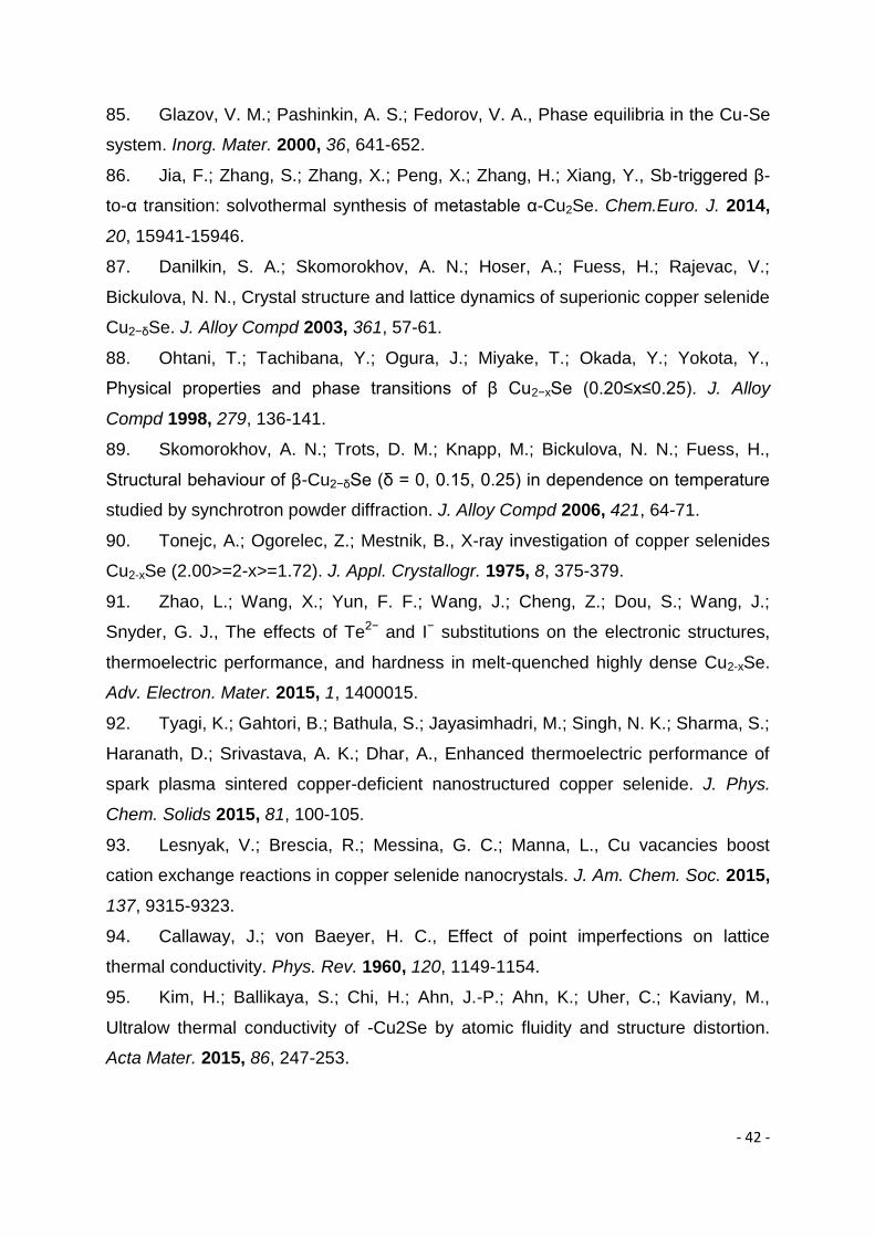
thermoelectric materials (shown in Figure 1.2).2, 8 It is worth to develop these
materials as well as to find new material systems. With the development of
nanotechnology in 1990s, an increasing number of researchers realized that
Page 25
- 3 -
nanostructures can boost the thermoelectric properties of many kinds of materials,5,
9, 10 which offered a new approach to achieve higher thermoelectric performance. It is
believed that current thermoelectric science could be further developed and
advanced high efficient thermoelectric materials will play a crucial role of power
generation and refrigeration in near future.
Figure 1.2 ZT values of different materials as a function of temperature.7
1.2 Objective and Scopes
To carry out this project, general understanding of the theories and principles of
thermolelectrics should be established to find out the vital factors which affect the
thermoelectric performance of materials. The main goal of this project is to develop a
low-cost, efficient, reliable and environmental friendly synthesis method of as-
designed high-efficiency thermoelectric materials. Specifically, in this project, metal
chalcogenides-based system with relatively superior thermoelectric properties will be
synthesized, characterized and analysed by appropriate methods.
Page 26
- 4 -
1.3 Thesis outline
To develop high performance metal chalcogenides-based thermoelectric
nanomaterials, Cu2Se, Bi2Te3 and PbTe-based nanomaterials have been
synthesized via facile and controllable solvothermal methods. The structures of the
as-prepared products were carefully investigated via advanced electron microscopy
and other methods. The products were then sintered and their thermoelectric
properties were analysed.
Chapter 1 is the introduction of this project.
Chapter 2 provides the literature review of previous studies about thermoelectric
materials. Some basic thermoelectric effects are introduced to help establishing the
understanding of effective factors for high performance thermoelectric materials. The
development of thermoelectric materials has been summarized. Then metal
chalcogenides thermoelectric candidates are focused due to their intrinsic high
thermoelectric performances and great potential on commercialization.
Chapter 3 introduces the relative experimental technologies used in this project.
Several popular synthesizing methods for nanomaterials were listed and compared
with each other. Solvothermal method is introduced in detail as the synthesis method
used in this project. Then some basic working principles of these experimental
technologies are introduced.
Chapter 4 demonstrates the controllable synthesis of metal chalcogenides
nanostructures and their thermoelectric performances. In this chapter, compositional
control of Cu2-xSe nanostructures and their thermoelectric properties, and phase
control of Cu2-xSe nanostructures triggered by Te-doping and their thermoelectric
properties have been carefully studied. This part includes two drafted manuscripts,
which have been submitted.
Chapter 5 focuses on enhanced thermoelectric performances of metal
chalcogenides via nanostructure engineering.
In the first part, nanostructure engineering was applied to enhance the thermoelectric
performance of Cu2Se nanomaterials. This part is included as the Nano Energy,
2015, 16, 367-374.
Page 27
- 5 -
The second part confirms the effectiveness of nanostructure engineering on Bi2Te3
nanomaterials. This part is included as ACS Applied Materials & Interfaces, 2015, 7
(42), 23694-23699.
The third part combines the doping and nanostructure engineering on PbTe,
carefully analysed the growth mechanism and the thermoelectric properties, which
has been drafted and ready to be submitted.
Chapter 6 gives the conclusion of this thesis with recommendations for future
development of thermoelectric materials.
Page 28
- 6 -
Chapter 2: Literature Review
In this chapter, fundamental thermoelectric effects and phenomena are presented to
address the basic factors which determine the thermoelectric performance of
materials. The conflict factors drawback the development of thermoelectric materials.
The approaches which can optimize the thermoelectric properties are then
demonstrated: to control the effective factors and choose appropriate materials
systems. Tellurium-based materials are focused due to their promising properties;
tellurium and lead telluride are studied in this project. The state-of-art researches
about tellurium-based materials are shown in this chapter.
2.1 Thermoelectric Effects
The conversion between temperature gradient and electricity was named as
thermoelectric effects. A series of theories have been developed by scientists to
describe and study thermoelectrics since the first thermoelectric effect was found by
Thomas Seebeck. The general principles of thermoelectrics are followed.
Page 29
- 7 -
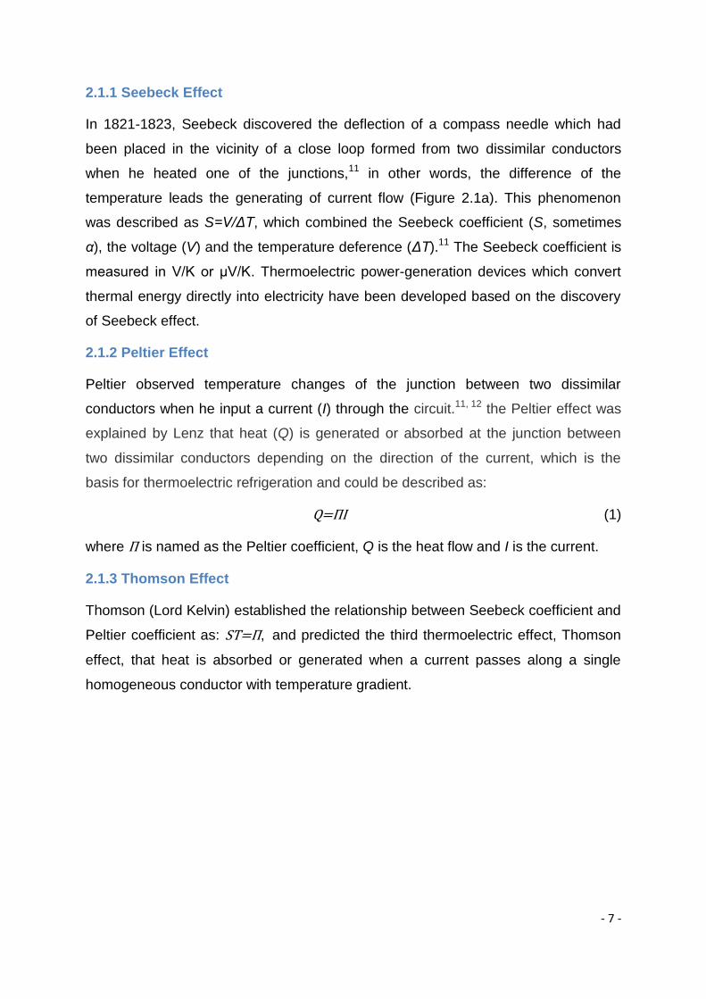
2.1.1 Seebeck Effect
In 1821-1823, Seebeck discovered the deflection of a compass needle which had
been placed in the vicinity of a close loop formed from two dissimilar conductors
when he heated one of the junctions,11 in other words, the difference of the
temperature leads the generating of current flow (Figure 2.1a). This phenomenon
was described as S=V/ΔT, which combined the Seebeck coefficient (S, sometimes
α), the voltage (V) and the temperature deference (ΔT).11 The Seebeck coefficient is
measured in V/K or μV/K. Thermoelectric power-generation devices which convert
thermal energy directly into electricity have been developed based on the discovery
of Seebeck effect.
2.1.2 Peltier Effect
Peltier observed temperature changes of the junction between two dissimilar
conductors when he input a current (I) through the circuit.11, 12 the Peltier effect was
explained by Lenz that heat (Q) is generated or absorbed at the junction between
two dissimilar conductors depending on the direction of the current, which is the
basis for thermoelectric refrigeration and could be described as:
Q=ΠI (1)
where Π is named as the Peltier coefficient, Q is the heat flow and I is the current.
2.1.3 Thomson Effect
Thomson (Lord Kelvin) established the relationship between Seebeck coefficient and
Peltier coefficient as: ST=Π, and predicted the third thermoelectric effect, Thomson
effect, that heat is absorbed or generated when a current passes along a single
homogeneous conductor with temperature gradient.
Page 30
- 8 -
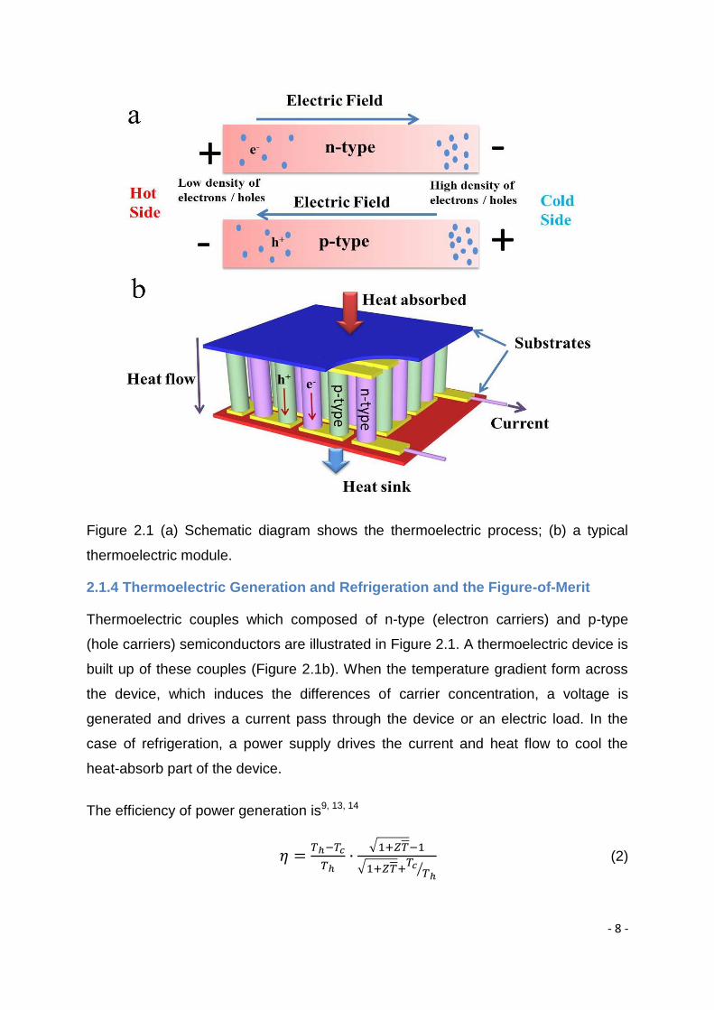
Figure 2.1 (a) Schematic diagram shows the thermoelectric process; (b) a typical
thermoelectric module.
2.1.4 Thermoelectric Generation and Refrigeration and the Figure-of-Merit
Thermoelectric couples which composed of n-type (electron carriers) and p-type
(hole carriers) semiconductors are illustrated in Figure 2.1. A thermoelectric device is
built up of these couples (Figure 2.1b). When the temperature gradient form across
the device, which induces the differences of carrier concentration, a voltage is
generated and drives a current pass through the device or an electric load. In the
case of refrigeration, a power supply drives the current and heat flow to cool the
heat-absorb part of the device.
The efficiency of power generation is9, 13, 14
=
√
√
⁄
(2)
Page 31
- 9 -
where is the average temperature of the hot-end temperature (Th) and the cold-
end temperature (Tc).
The coefficient of performance (COP) for a refrigeration mode is9, 15
=
√
⁄
√ (3)
To judge the thermoelectric performance, figure-of-merit can be defined:
= (4)
Where Z is the figure-of-merit, the unit of Z is 1/K. T is the absolute temperature, S is
the Seebeck coefficient, σ is the electrical conductivity and κ is the thermal
conductivity. S2σ is the electrical power factor.
From these equations above, it is clear that higher thermoelectric performance relate
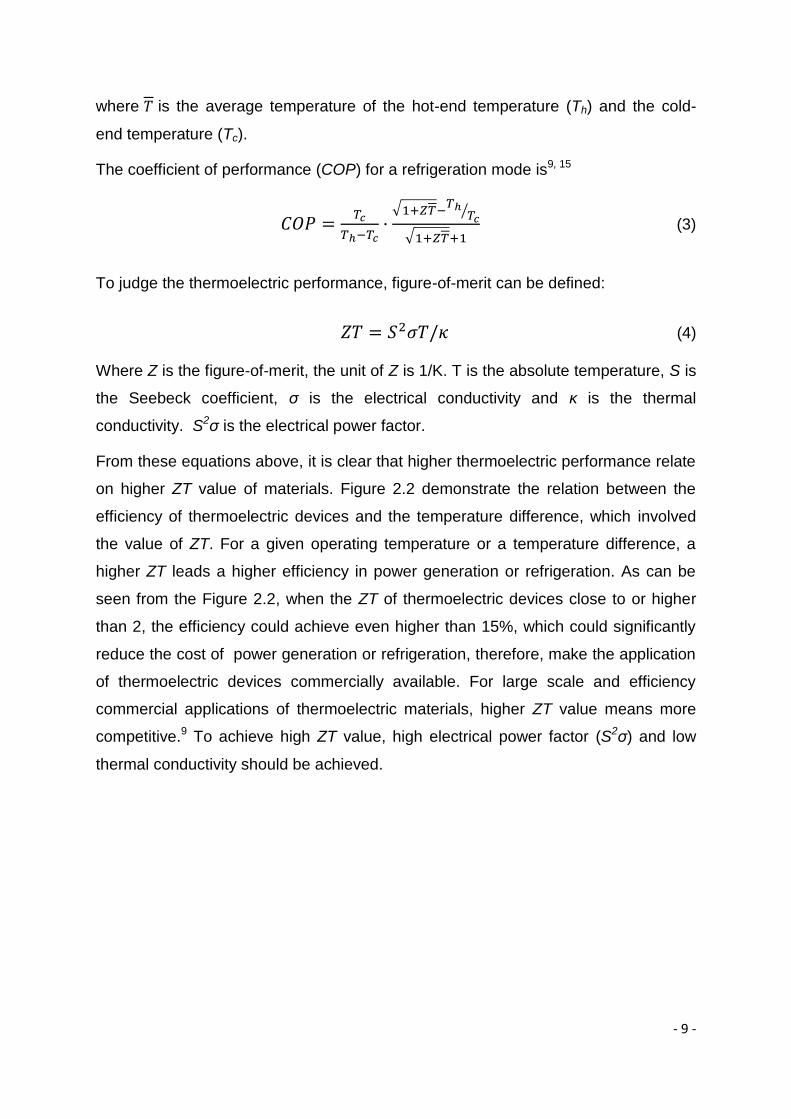
on higher ZT value of materials. Figure 2.2 demonstrate the relation between the
efficiency of thermoelectric devices and the temperature difference, which involved
the value of ZT. For a given operating temperature or a temperature difference, a
higher ZT leads a higher efficiency in power generation or refrigeration. As can be
seen from the Figure 2.2, when the ZT of thermoelectric devices close to or higher
than 2, the efficiency could achieve even higher than 15%, which could significantly
reduce the cost of power generation or refrigeration, therefore, make the application
of thermoelectric devices commercially available. For large scale and efficiency
commercial applications of thermoelectric materials, higher ZT value means more
competitive.9 To achieve high ZT value, high electrical power factor (S2σ) and low
thermal conductivity should be achieved.
Page 32
- 10 -
Figure 2.2 Efficiency of thermoelectric devices as a function of ΔT.7
2.1.5 Effective Factors
The principles of the achievement high figure-of-merit or high thermoelectric
performance are complicated. By analysing the thermoelectric principles, the
effective factors of thermoelectric properties can be targeted to efficiently optimize
the thermoelectric performance of materials. Basically, a material which has a high
thermoelectric performance should have an appropriate carrier concentration and a
low thermal conductivity. Tuning the carrier concentration and thermal conductivity
through various methods is an efficient way to adjust the thermoelectric properties of
materials.
2.1.5.1 Carrier Concentration
To a great extent, electrical power factor (S2σ) determines the thermal function of
materials. So we should ensure that high Seebeck coefficient and high electrical
conductivity could be achieved synchronously. Both Seebeck coefficient (S) and
electrical conductivity (σ) relate to the carrier concentration of materials.16
=
⁄ (5)
Page 33
- 11 -
= ⁄ = (6)
Where n is the carrier concentration of materials, is the effective mass of the
carrier, ρ is the electric resistivity, e is the electrical charge of an electron, and kB is
the Boltzmann constant and μ is the carrier mobility. Specifically, μ is the function of
E (the magnitude of the electric field applied to a material) and vd (the magnitude of
the electron drift velocity caused by the electric field). These equations show us that
lower carrier concentration leads lower electric conductivity but higher Seebeck
coefficient.
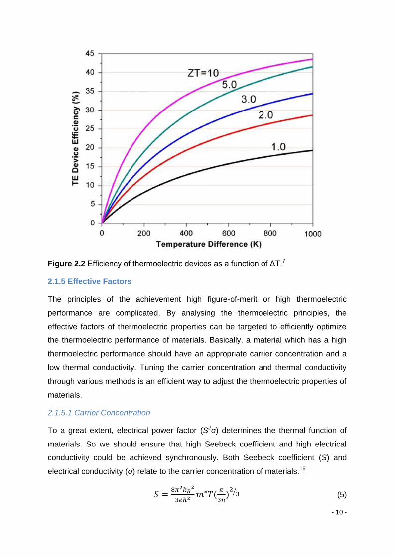
Figure 2.3 The relation between carrier concentration and the value of ZT.16
It is hard to achieve a high Seebeck coefficient with a high electrical conductivity due
to the complex connection of S, σ and n. Figure 2.3 shows that maximizing the ZT of
Bi2Te3 thermoelectric materials involves a compromise of the conflicting properties
(Seebeck coefficient, electronic conductivity and thermal conductivity). As the
thermal conductivity is also the function of carrier concentration, optimizing the
carrier concentration is crucial for maximizing the value of ZT. For an ideal
thermoelectric material which has been typically heavily doped, the carrier
concentration is between 1019 and 1021.
2.1.5.2 Thermal Conductivity
Thermal conductivity of materials comes from two sources16: electrons and holes
transporting heat (κe) and lattice thermal conductivity (κL):
Page 34
- 12 -
= (7)
= = (8)
where L is Lorenz factor, 2.4×10⁻⁸ J2K-2C-2 for free electrons. As the electronic
thermal conductivity is directly related to the electric conductivity, κe should be
maintained at a high level while the thermal conductivity should be reduced for
achieving higher figure-of-merit.
2.1.5.3 Achieve High ZT
Theoretically, thermoelectrics require materials with high electrical power factor (S2σ)
and low thermal conductivity; furthermore, high electronic properties and low lattice
thermal conductivity17 should be achieved. These kind of special materials are called
a phonon-glass electron-crystal.6 Many crystalline semiconductors are identified as
good thermoelectric materials.18-23 In recent years, high ZT (>1) was extensively
achieved in heavily doped semiconductors,8, 16, 24 superlattice structures24-27 as well
as nanostructures.1, 5, 10, 24
State-of-the-art high ZT materials have been achieved by the using of nano-
technology. Both nano-miniaturization and nanocomposites are proved as efficient
approaches for the enhancement of thermoelectric properties, which are suggested
to increase the Seebeck coefficient and decrease the lattice thermal conductivity due
to the quantum confinement and the strong scattering to phonons. The theory and
principle will be discussed in the part of 2.3.
2.2 Development of Thermoelectric Materials
Since the thermoelectric effects were discovered, a large number of materials have
already been tested as thermoelectric candidates. Bi-Sb alloy system,28-32 Bi-Te
system,31, 33-39 Pb-Te system,40-48 Si-Ge system,49-52 some complex oxides2, 53 and
complex minerals with phonon-glass electron-crystal structure such as
Skutterudites8, 54-56 were considered as good thermoelectric materials, their ZT
values were experimentally measured as shown in Figure 2.4.
Page 35
- 13 -
Figure 2.4 ZT as a function of temperature for several high-efficiency bulk
thermoelectric materials
(http://chemgroups.northwestern.edu/kanatzidis/greatthermo.html).
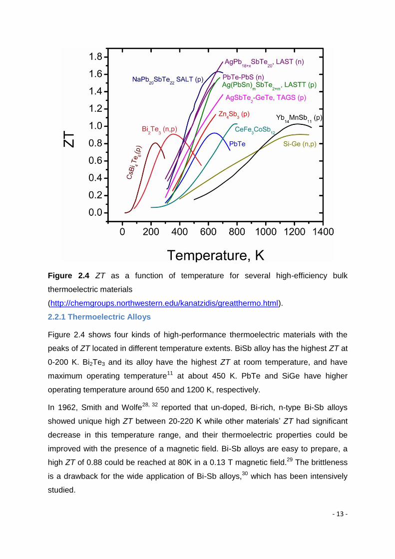
2.2.1 Thermoelectric Alloys
Figure 2.4 shows four kinds of high-performance thermoelectric materials with the
peaks of ZT located in different temperature extents. BiSb alloy has the highest ZT at
0-200 K. Bi2Te3 and its alloy have the highest ZT at room temperature, and have
maximum operating temperature11 at about 450 K. PbTe and SiGe have higher
operating temperature around 650 and 1200 K, respectively.
In 1962, Smith and Wolfe28, 32 reported that un-doped, Bi-rich, n-type Bi-Sb alloys
showed unique high ZT between 20-220 K while other materials’ ZT had significant
decrease in this temperature range, and their thermoelectric properties could be
improved with the presence of a magnetic field. Bi-Sb alloys are easy to prepare, a
high ZT of 0.88 could be reached at 80K in a 0.13 T magnetic field.29 The brittleness
is a drawback for the wide application of Bi-Sb alloys,30 which has been intensively
studied.
Page 36
- 14 -
Bi2Te3 is the best thermoelectric materials in the range of 300-500 K and had been
commercially applied in refrigeration devices for many years.57 Bi2Te3-based
thermoelectric materials can not only be used in room temperature but also can be
used for lower temperature applications by being doped. In 2000, Chung58 and co-
workers developed a new Bi-Te system material: CsBi4Te6 which achieved a
maximum ZT of ~0.8 at 225 K. This work pointed out a new approach to expand the
application temperature of thermoelectric materials. The new enhancement of bulk
materials’ thermoelectric properties could be expected.
The PbTe-based alloys have been extensively used for power generation, small-
scale cooling even power supplies for space exploration43, 59 due to their outstading
thermoelectric properties in middle temperature range. PbTe has a FCC crystal
structure with the band gap of ~0.32 eV at room temperature. PbTe could reach a ZT
of 0.8 near 550K, which could be significantly increased by doping or forming alloys
or soild solution. Poudeu60 and co-workers reported a ZT of 1.5 in Pb0.96Sb0.2Te10-
xSex system at 800K when x=7. In Poudeu’s another work,61 they also achieved very
high ZT in the system of Na1-xPbmSbyTem+2.
Si-Ge alloys are the best thermoelectric materials in high temperature arange (over
700 K), with a ZT of ~0.8 at around 1100 K (Figure 2.4). The thermoelectric
properties of Si-Ge alloys could be adjusted through changing the ratio of Si and Ge,
the conventional ratio is around Si80Ge20. Recntly, nanostructural SiGe62 has been
widely studied as well as bulk SiGe.
In additon, nowadays, the field of bulk thermoelectric materials are not limited on
these simple alloys or solid solution systems, more people have paid attention to
alloys with multiconponents, such as Ag-Sn-Sb-Te system63, (GeTe)(x)(AgSbTe2)(100-
x),64 Zn4Sb3/Bi0.5Sb1.5Te3
65 and complex oxides like La1−xSrxCoO366, NaCo2O4.
67
Hsu68 and co-workers achieved a ZT of 2.2 in AgPbmSbTe2+m , which showed us a
bright future of bulk thermoelectric materials. As high ZT of these materials have
been achieved in these materials, their extensive thermoelectric application in future
could be expected.
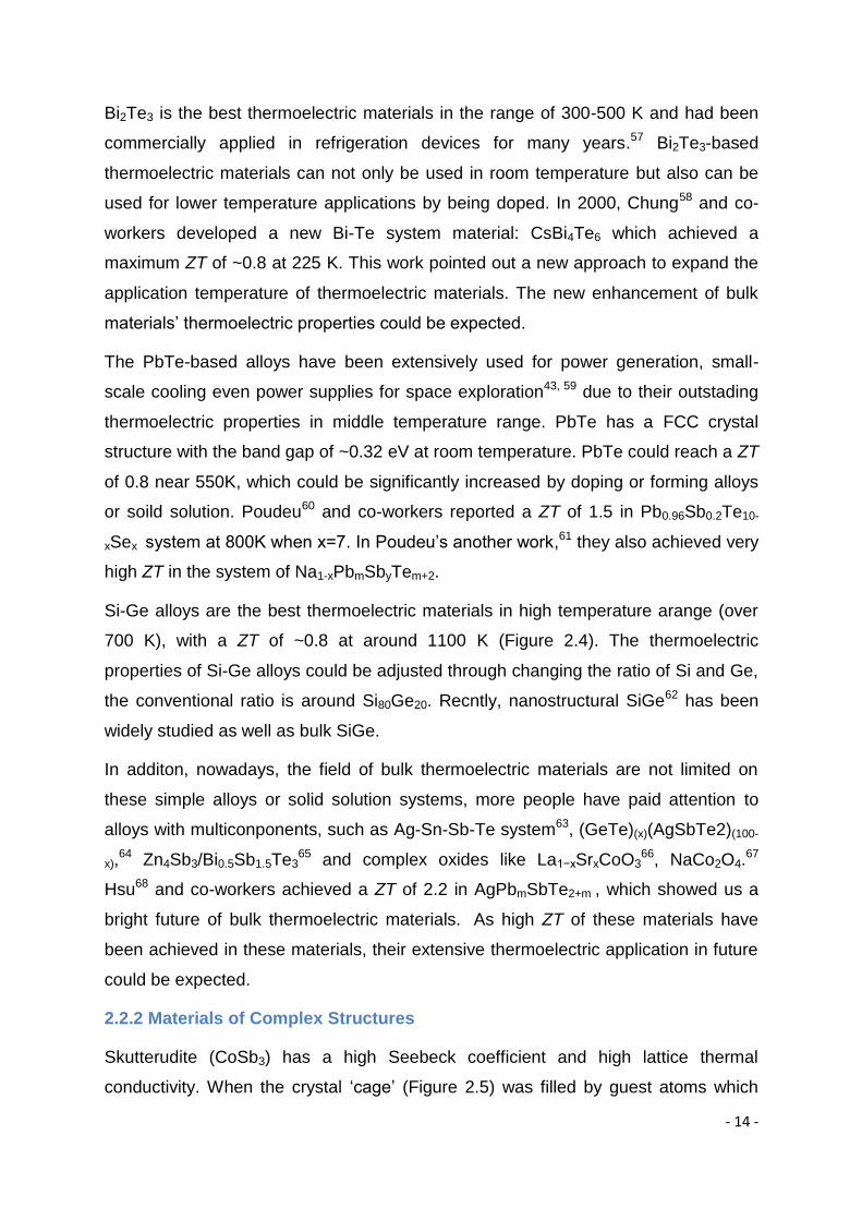
2.2.2 Materials of Complex Structures
Skutterudite (CoSb3) has a high Seebeck coefficient and high lattice thermal
conductivity. When the crystal ‘cage’ (Figure 2.5) was filled by guest atoms which
Page 37
- 15 -
could bring the thermal conductivity down due to their fremitus in lattice, the
thermoelectric properties will be significantly improved. Figure 2.5d shows that the
highest ZT value of Co4Sb12 is 0.2 at 500 K. The thermoelectric property of Co4Sb12
was boosted to a very high level (>1) in a larger temperature extent after it was
doped by some other elements.
There are two types of Clathrates (I and II), both of them have low thermal
conductivities and open framework which could incorporate large electropositive
atoms. The principle of improving the ZT of Clathrates is similar as in the case of
Skutterudites.
Figure 2.5.(a-c) Crystal structure of CoSb3 revealing the large voids with rattlers, the
type-I Clathrate Na8Si46, and β-Zn4Sb3; (d) ZT as a function of temperature for
skutterudites as thermoelectric materials; (e) Variable temperature ZT of Clathrates,
and β-Zn4Sb3.69
2.2.3 Metal Chalcogenides Thermoelectric Materials
Metal chalcogenides materials are considered as ideal thermoelectric materials
which have shown promising thermoelectric properties in a wide range of applying
temperature. Among them, the best-performed thermoelectric material in a broad
Page 38
- 16 -
temperature range, namely, copper selenide (800-1000 K), lead telluride (500-800 K)
and bismuth telluride (300-400 K) are extensively studied.
2.2.3.1 Cu2Se-based Thermoelectric Materials
Copper chalcogenides Cu2-xX (X= S, Se or Te) have been realized as a group of
promising thermoelectric materials due to their unique properties70-76 in last several
years, especially Cu2Se, which can be applied in photovoltaics,77 thermoelectrics,71,
78 photocatalyst,79 gas sensoring,80 electrode81 and superionic conductors.82
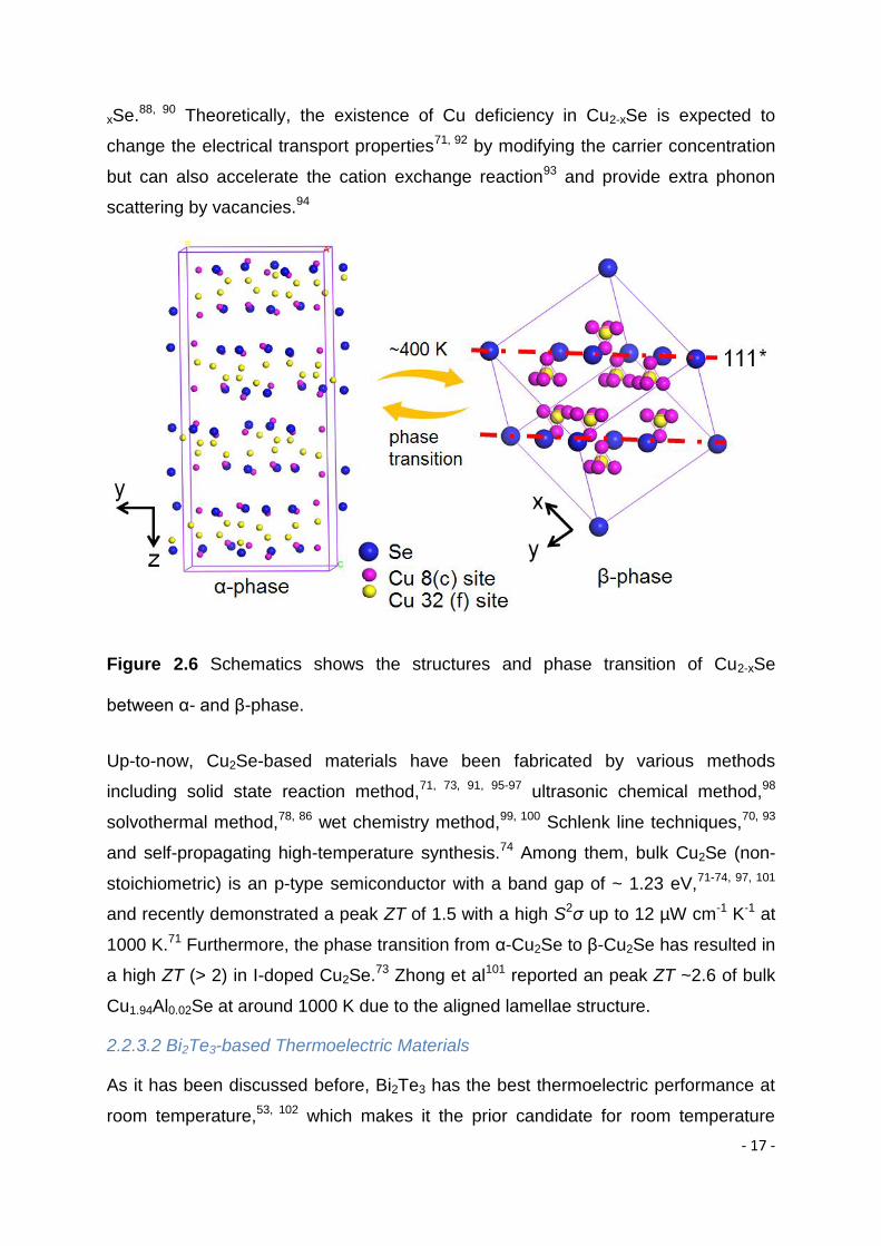
Generally, Cu2Se shows an α-phase when the temperature is lower than 400 K, it
has a monoclinic crystal structure with lattice parameters of a = 0.7138 nm, b =
1.238 nm, c = 2.739 nm, β = 94.308°, in which Cu ions are fixed in 12 positions
within the Se frame.83 When the temperature is increased and reaches to above 400
K, α-Cu2Se transfers to a β-phase with a lattice parameter a = 0.58 nm and the
space group ,71, 73, 84, 85 which can be demonstrated in Figure 2.6. Such a
phase transformation is reversible through cooling or heating processes. During the
phase transformation, Se ions formed a face-centre-cubic (FCC) frame and Cu+ ions
partially occupied86, 87 the 8(c) and 32(f) interstitial sites,86-90 these Cu+ ions are
highly mobile and exhibiting super-ionic liquid-like behaviour, which is crucial for its
intrinsically low κL because the phonons will be strongly scattered by such liquid-like
ions and finally lead to a high ZT of Cu2Se.71, 78
Interestingly, kinetically favoured β-Cu2Se was found as the preferred phase for
nanostructured Cu2Se product at room temperature rather than α-Cu2Se.78, 86 The
reason could be that the nanostructured Cu2Se has different surface energy state
compared with bulk materials.86 However, the phase transition from β- to α-phase
can be triggered by doping other elements such as Sb86 under certain condition. For
the Cu2Se-based materials, the stoichiometry is crucial for their structures and TE
performance.71, 91, 92 According to theoretical calculation,91 the stoichiometric Cu2Se
is a zero-gap material, significant Cu deficiency in β-Cu2-xSe can be allowed71, 90 to
form the non-stoichiometric Cu2-xSe (x=0-0.25)87 materials, which become intrinsic p-
type semiconductors with modified band structure. The existence of Cu deficiency
was found to affect the phase transition temperature88 and cause structural and
phase change87-90 of bulk Cu2-xSe compared to the stoichiometric Cu2Se. Low
temperature β-phase can be found in the composition range of 0.15≤x≤0.25 in Cu2-
3Fm m
Page 39
- 17 -
xSe.88, 90 Theoretically, the existence of Cu deficiency in Cu2-xSe is expected to
change the electrical transport properties71, 92 by modifying the carrier concentration
but can also accelerate the cation exchange reaction93 and provide extra phonon
scattering by vacancies.94
Figure 2.6 Schematics shows the structures and phase transition of Cu2-xSe
between α- and β-phase.
Up-to-now, Cu2Se-based materials have been fabricated by various methods
including solid state reaction method,71, 73, 91, 95-97 ultrasonic chemical method,98
solvothermal method,78, 86 wet chemistry method,99, 100 Schlenk line techniques,70, 93
and self-propagating high-temperature synthesis.74 Among them, bulk Cu2Se (non-
stoichiometric) is an p-type semiconductor with a band gap of ~ 1.23 eV,71-74, 97, 101
and recently demonstrated a peak ZT of 1.5 with a high S2σ up to 12 µW cm-1 K-1 at
1000 K.71 Furthermore, the phase transition from α-Cu2Se to β-Cu2Se has resulted in
a high ZT (> 2) in I-doped Cu2Se.73 Zhong et al101 reported an peak ZT ~2.6 of bulk
Cu1.94Al0.02Se at around 1000 K due to the aligned lamellae structure.
2.2.3.2 Bi2Te3-based Thermoelectric Materials
As it has been discussed before, Bi2Te3 has the best thermoelectric performance at
room temperature,53, 102 which makes it the prior candidate for room temperature
Page 40
- 18 -
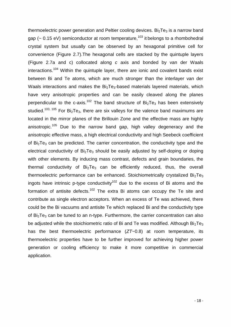
thermoelectric power generation and Peltier cooling devices. Bi2Te3 is a narrow band
gap (~ 0.15 eV) semiconductor at room temperature,103 it belongs to a rhombohedral
crystal system but usually can be observed by an hexagonal primitive cell for
convenience (Figure 2.7).The hexagonal cells are stacked by the quintuple layers
(Figure 2.7a and c) collocated along c axis and bonded by van der Waals
interactions.104 Within the quintuple layer, there are ionic and covalent bands exist
between Bi and Te atoms, which are much stronger than the interlayer van der
Waals interactions and makes the Bi2Te3-based materials layered materials, which
have very anisotropic properties and can be easily cleaved along the planes
perpendicular to the c-axis.102 The band structure of Bi2Te3 has been extensively
studied.103, 105 For Bi2Te3, there are six valleys for the valence band maximums are
located in the mirror planes of the Brillouin Zone and the effective mass are highly
anisotropic.105 Due to the narrow band gap, high valley degeneracy and the
anisotropic effective mass, a high electrical conductivity and high Seebeck coefficient
of Bi2Te3 can be predicted. The carrier concentration, the conductivity type and the
electrical conductivity of Bi2Te3 should be easily adjusted by self-doping or doping
with other elements. By inducing mass contrast, defects and grain boundaries, the
thermal conductivity of Bi2Te3 can be efficiently reduced, thus, the overall
thermoelectric performance can be enhanced. Stoichiometrically crystalized Bi2Te3
ingots have intrinsic p-type conductivity102 due to the excess of Bi atoms and the
formation of antisite defects.102 The extra Bi atoms can occupy the Te site and
contribute as single electron acceptors. When an excess of Te was achieved, there
could be the Bi vacuums and antisite Te which replaced Bi and the conductivity type
of Bi2Te3 can be tuned to an n-type. Furthermore, the carrier concentration can also
be adjusted while the stoichiometric ratio of Bi and Te was modified. Although Bi2Te3
has the best thermoelectric performance (ZT~0.8) at room temperature, its
thermoelectric properties have to be further improved for achieving higher power
generation or cooling efficiency to make it more competitive in commercial
application.
Page 41
- 19 -
Figure 2.7 Rhombohedral crystal structure of Bi2Te3.69
Different elements have been doped into Bi2Te3 crystal matrix to modify the
thermoelectric performance of Bi2Te3. In bulk materials, Sb and Se have been
successfully doped into Bi2Te3. A peak ZT of 1.4 has been achieved in p-type
(BiSb)2Te3 material at 373 K106 and a peak ZT of 1.56 has been obtained in
Bi0.52Sb1.48Te3 at 300 K.107 The highest ZT of (BiSb)2Te3 material had been reached
to as high as 1.8 at 316 K.108 In n-type bulk materials, a peak ZT of 1.04 was
observed in Bi2Te2.7Se0.3 at about 400 K and the ZT can be further increased to
about 1.1 by Cu doping.109, 110 The Seebeck Coefficients and the electrical
conductivities of those doped Bi2Te3-based materials have been obviously enhanced
while their thermal conductivities were significantly reduced. However, it is getting
harder to improve the thermoelectric performance of bulk Bi2Te3-based materials due
to the conflict relation between their thermoelectric properties. More and more
attention has been paid on nano-structured Bi2Te3 materials. Low-dimensional
Bi2Te3 materials have been intensively studied in recent years and many promising
Page 42
- 20 -
results have been achieved.111-115 The main approach for improving the
thermoelectric performance of Bi2Te3 still lies on the increase of its electrical
conductivity and Seebeck coefficient while decrease the thermal conductivity. The
obtained ZT values of Bi2Te3 nanomaterials are still lower than that of doped bulk
materials, but the enhancement of ZT compared with pure Bi2Te3 are encouraging,
and the ZT can be expected to achieve a higher level in the future.
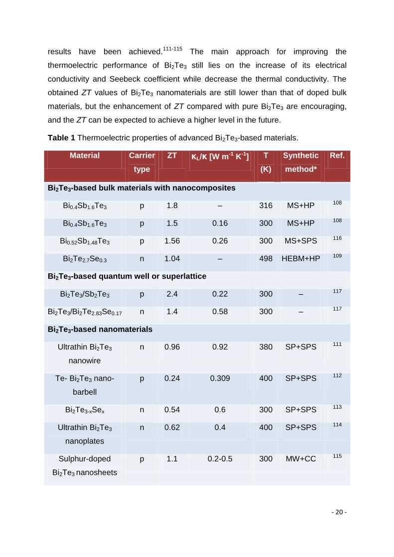
Table 1 Thermoelectric properties of advanced Bi2Te3-based materials.
Material Carrier
type
ZT κL/κ [W m-1 K-1] T
(K)
Synthetic
method*
Ref.
Bi2Te3-based bulk materials with nanocomposites
Bi0.4Sb1.6Te3 p 1.8 – 316 MS+HP 108
Bi0.4Sb1.6Te3 p 1.5 0.16 300 MS+HP 108
Bi0.52Sb1.48Te3 p 1.56 0.26 300 MS+SPS 116
Bi2Te2.7Se0.3 n 1.04 – 498 HEBM+HP 109
Bi2Te3-based quantum well or superlattice
Bi2Te3/Sb2Te3 p 2.4 0.22 300 – 117
Bi2Te3/Bi2Te2.83Se0.17 n 1.4 0.58 300 – 117
Bi2Te3-based nanomaterials
Ultrathin Bi2Te3
nanowire
n 0.96 0.92 380 SP+SPS 111
Te- Bi2Te3 nano-
barbell
p 0.24 0.309 400 SP+SPS 112
Bi2Te3-xSex n 0.54 0.6 300 SP+SPS 113
Ultrathin Bi2Te3
nanoplates
n 0.62 0.4 400 SP+SPS 114
Sulphur-doped
Bi2Te3 nanosheets
p 1.1 0.2-0.5 300 MW+CC 115
Page 43
- 21 -
*The abbreviations used in the column of the synthetic method represent the
following meanings: MS= melt spinning; HP= hot pressing; HEBM= high energy ball
milling; SPS= spark plasma sintering; SP= solution phase method; MW= microwave
synthesis; CC= cold compaction.
2.2.3.3 PbTe-based Thermoelectric Materials
PbTe is a well-known IV-VI semiconductor with a narrow band gap (~0.3 eV) at room
temperature and large average excitonic Bohr radius of ~46 nm.118, 119 The crystal
structure of PbTe is face-centre-cubic. Because of the narrow band gap and the
large Bohr radius, a strong quantum confinement could exist in a large size range
(depend on the Bohr radius). In addition, PbTe has a lot of good physical and
chemical properties. It has high melting point, low vapour pressure, good chemical
stability and high ZT.119, 120 Furthermore, lead telluride can be easily doped to form
both n-type and p-type semiconductors. The self-doping of PbTe could be achieved
by varying the stoichiometry of lead and tellurium to modify the semi-conductive
property. The band gap of PbTe can also be adjusted by doping or alloying with
other elements. For instance, the band gap of PbTe will be reduced if it is alloyed
with Sn, or be increased by alloying it with Eu.118
The history that PbTe was used as practical thermoelectric materials can be tracked
back to 1930s.121, 122 In 1960s, both p- and n-type PbTe were used to assemble the
RTG for powering the spacecraft launched by The National Aeronautics and Space
Administration (NASA).121 Although the concentration had been shifted to Si-Ge
thermoelectric materials duo to their higher working temperature (above 1000 K) for
several years, the interest of lead telluride-based materials has recently been
reinvigorated because of their stability and promising thermoelectric efficiency. In
NASA’s latest Mars rover mission, PbTe-based materials were again chosen for
power supply.122
Lead telluride is a kind of covalent intermetallic compound with intrinsic low thermal
conductivity and good electrical properties.123 The FCC PbTe can be easily doped to
obtain n-type or p-type PbTe-based semiconductors with the implement of optimizing
their carry concentration, even the mechanical strength enhancement could be
achieved124 by doping or alloying. Both p- and n-type PbTe show the highest ZT in
the intermediate temperature range (500-900K) in all candidates of thermoelectric
Page 44
- 22 -
materials,53 this operational temperature range is far below the melting point of PbTe
(1195 K).
The lightly doped p-type (by sodium) and n-type (by iodine) PbTe were
systematically studied and the peak ZT value of 0.7 for p-type and 0.8 for n-type
PbTe were found by Fritts123 in 1960. Limited by the approach of thermal conductivity
measurement, Fritts used the thermal conductivity measured at room temperature to
calculate the ZT values in the whole investigated temperature range. He realized that
the thermal conductivities were overestimated for high temperature and suggested
that the true ZT values should be higher.123 The reinvestigation of Na-doped PbTe
and I-doped PbTe had been done;125, 126 the laser flash method was introduced to
measure the thermal conductivity. The results showed the peak ZT value as 1.4
rather than 0.7 or 0.8. The doping level of PbTe was also proved could be further
optimized.
The outstanding thermoelectric performance of PbTe and PbTe-based materials
comes from the unique band structure of PbTe. With a high symmetry face-centre-
cubic crystal structure, convergence of many valleys can arise in PbTe.127 The high
valley degeneracy (Nv) lead a high Seebeck coefficient, thus, a high ZT.127
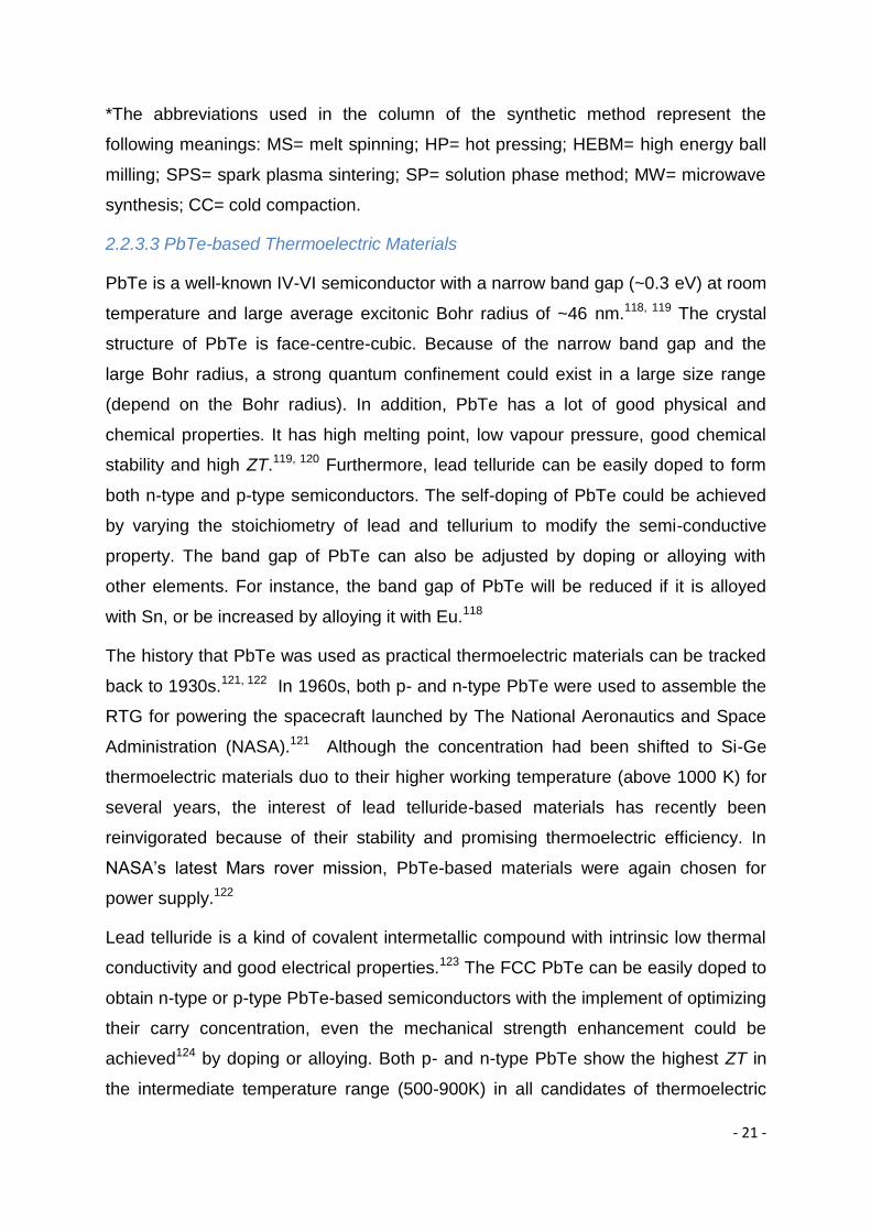
A two valence band model (Figure 2.8) of PbTe was suggested in 1960s.128, 129
When the band gap of PbTe was studied, it was found that ⁄ ( is the band
gap while T is the absolute temperature) was approximately zero at high temperature
range (above 450 K) while the ⁄ value was 4.1×10⁻⁴ eV/°K at low
temperature.128 This indicated that a principle valence band (L band, located at the L
point of the Brillouin zone) active at low temperature and a secondary valence band
(Σ band, located at the Σ point of the Brillouin zone) dominate at temperature higher
than 450 K.130 There is an energy separation of about 0.2 eV of these two valence
bands and the L band and Σ band were found to have valley degeneracies of 4 and
12, respectively.121, 127, 131 With the temperature increasing, the L band moves
converging with Σ band at about 450 K and providing an overall valley degeneracy of
16, which will greatly benefit to the thermoelectric performance of PbTe. When the L
band keeps moving below the Σ band, the dominating Σ band will still provide a
valley degeneracy of 12. The convergence temperature of these two valence band
Page 45
- 23 -
was found could be adjusted by alloying or doping PbTe with another elements such
as Se,127 to broaden the applying temperature range of PbTe-based materials.
Figure 2.8 Valence band structure of PbTe1-xSex. (a) Brillouin zone showing the low
degeneracy hole pockets (orange) centred at the L point, and the high degeneracy
hole pockets (blue) along the Σ line. (b) Relative energy of the valence bands in
PbTe0.85Se0.15. At 500K the two valence bands converge, resulting in transport
contributions from both the L and Σ bands.47
The intrinsic high valley degeneracy and tuneable band structure makes PbTe as an
ideal candidate of high performance thermoelectric materials. Extensive efforts have
been made to obtain PbTe-based thermoelectric materials with high ZT value. Table
1 shows several advanced thermoelectric materials based on PbTe, high ZT values
were achieved in these materials by various methods in a large temperature range
(room temperature to 800 K), which makes the PbTe-based materials more
competitive compared with other potential thermoelectric materials used in the
intermediate temperature range (500-900 K).
So far, most studies of the thermoelectric performance of PbTe-based materials
have been focused on bulk materials because bulk materials are easy to be
prepared and their properties can be accurately measured compared with low-
dimensional materials. However, the peak ZT value of bulk materials is very hard to
achieve 2 or greater due to the conflict electrical and thermal properties which
determined the thermoelectric performance. With the development nano-science,
both theoretical25 and experimental26 studies suggested that it is expected to achieve
Page 46
- 24 -
substantial ZT in low-dimensional materials. In last two decades, PbTe
nanomaterials have been paid much attention in synthesis and the improvement of
thermoelectric performance.
Up to now, various morphologies of PbTe such as nanospheres,132 nanowires,118, 133
nanosheets,134, 135 nanorods,136 nanoboxes,21 nanotubes,132, 137 nanoparticles,135, 138
hierarchical nanostructures139 and thicket-like119 nanostructures have been
fabricated by many methods. Molecular Beam Epitaxy (MBE),118 chemical vapour
deposition (CVD),140, 141 electrochemical deposition,119, 142 solvothermal or
hydrothermal43, 143, 144 methods are intensively used to prepare nanostructured PbTe
and its alloys or doped PbTe. Besides to form nanostructures such as quantum dots
to change the electronic density of states and reduce the lattice thermal conductivity
and increase the electrical power factor, one of other efficient approaches to
enhance the thermoelectric properties of lead telluride is to dope PbTe with some
other elements. The doping atoms can cause the distortion of not only the crystal
lattice but also the electronic density of states,46 which could also decrease the
thermal conductivity of the materials.
Solvothermal method has been identified as an efficient approach for synthesizing
PbTe with highly controllable processes. Well-crystallized lead telluride
nanostructures with variety of morphologies have been extensively fabricated and
reported and very high thermoelectric performances are expected to be achieved on
these PbTe nanostructures.
This project mainly concentrates on the understanding of experimental methodology,
the synthesis of nanostructured thermoelectric materials and to improve the
thermoelectric performance of PbTe-based nanomaterials. PbTe nanostructures
have been synthesized through a solvothermal route, and have been doped to
modify the carrier concentration and band structure. The samples have been
characterized by X-ray diffraction (XRD), scanning electron microscope (SEM) and
transmission electron microscope (TEM) to analyse their structures.
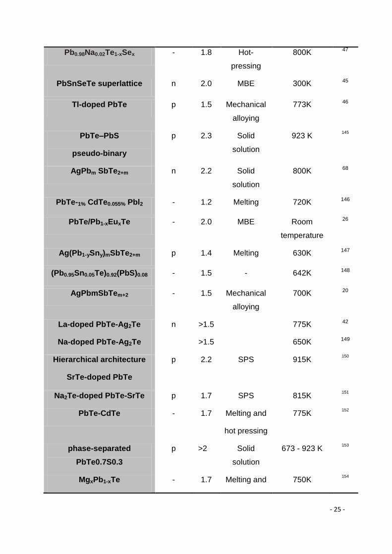
Table 2 Advanced thermoelectric materials in Pb-Te system
Materials Type of
carriers
ZT Synthesis
method
Temperature Ref.
Page 47
- 25 -
Pb0.98Na0.02Te1-xSex - 1.8 Hot-
pressing
800K 47
PbSnSeTe superlattice n 2.0 MBE 300K 45
Tl-doped PbTe p 1.5 Mechanical
alloying
773K 46
PbTe–PbS
pseudo-binary
p 2.3 Solid
solution
923 K 145
AgPbm SbTe2+m n 2.2 Solid
solution
800K 68
PbTe-1% CdTe0.055% Pbl2 - 1.2 Melting 720K 146
PbTe/Pb1-xEuxTe - 2.0 MBE Room
temperature
26
Ag(Pb1-ySny)mSbTe2+m p 1.4 Melting 630K 147
(Pb0.95Sn0.05Te)0.92(PbS)0.08 - 1.5 - 642K 148
AgPbmSbTem+2 - 1.5 Mechanical
alloying
700K 20
La-doped PbTe-Ag2Te n >1.5 775K 42
Na-doped PbTe-Ag2Te >1.5 650K 149
Hierarchical architecture
SrTe-doped PbTe
p 2.2 SPS 915K 150
Na2Te-doped PbTe-SrTe p 1.7 SPS 815K 151
PbTe-CdTe - 1.7 Melting and
hot pressing
775K 152
phase-separated
PbTe0.7S0.3
p >2 Solid
solution
673 - 923 K 153
MgxPb1-xTe - 1.7 Melting and 750K 154
Page 48
- 26 -
hot pressing
2.3 Principles and Methodologies to Achieve
High ZT
Based on the introduction of materials which intrinsically have high thermoelectric
performances, some necessary requirement for high performance thermoelectric
materials can be revealed: good σ, high S for electronic transport and low κ for
maintaining the temperature difference. Some other materials with such nature can
also be applied in thermoelectrics. However, pristine materials rarely achieve the ZT
above unity,7 which limits the application of thermoelectric materials and raises the
urgent demand to enhance their thermoelectric performances and implement the
commercialization.
2.3.1 Optimize the Carrier Concentration
The ideal thermoelectric materials could be described as ‘phonon-glass electron-
crystal’,155 which requires the κ as low as glass-like materials and the electrical
transport properties as good as crystalline materials.7 According to this principle,
several strategies can be applied to improve ZT of bulk materials, in which the most
effective approaches are to improve the electrical transport properties via optimizing
the carrier concentration and band engineering, which can decouple the σ and S,
therefore, achieve high power factor.
Among all the parameters which affect the thermoelectric performance of materials,
the S, σ and κe directly relate with n and are coupled by n as shown in equations (5),
(6) and (8), which makes controlling the carrier concentration a crucial strategy to
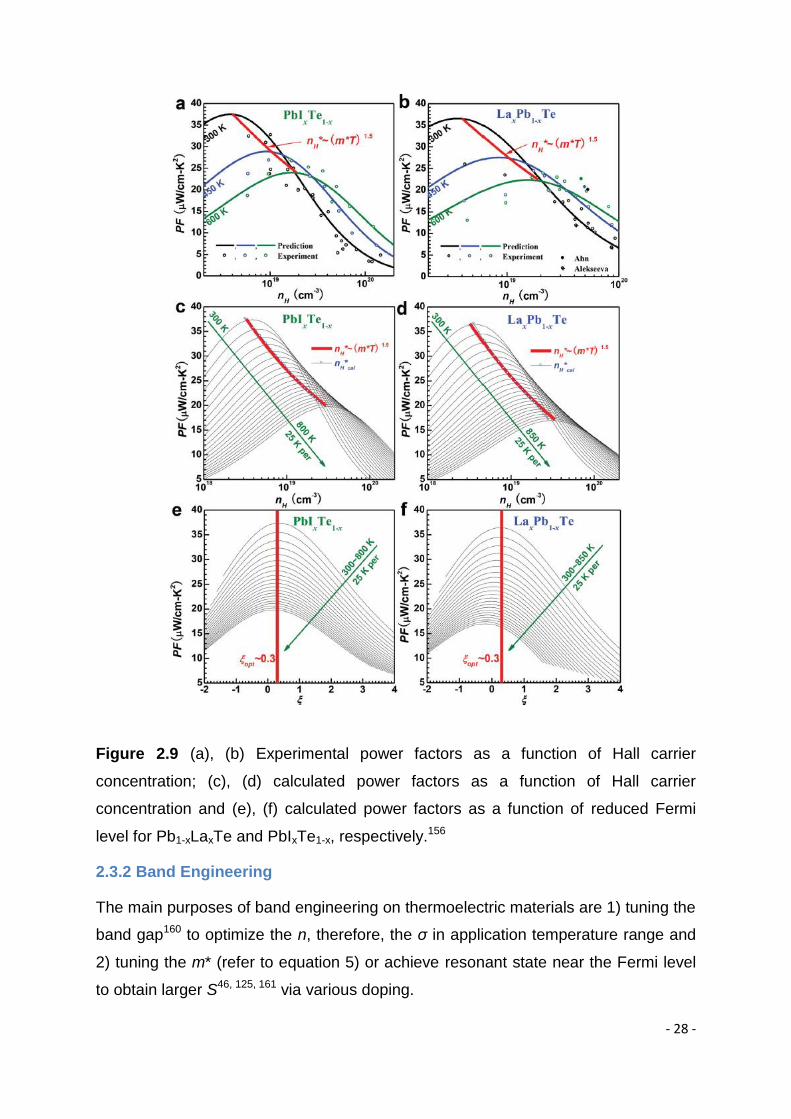
obtain high ZT. It is important to realize that the optimal carrier concentration (n*) is
strongly temperature dependent for most thermoelectric candidate as they are
semiconductors,156 so that the n* for different materials should greatly depend on
their application temperature.156 To provide a simplified prediction of the n*, the
relation n*~ (m*T)1.5 was suggested157 based on single band model and classic
statistics equations, where m* is the effective mass of carriers. According to this
Page 49
- 27 -
relation, thermoelectric materials applied in lower temperature range should have
lower n* compared to materials which can be applied in higher temperature range.
For example, Bi2Te3158 has n ~1019 at room temperature while Cu2Se has the room
temperature n over 1020.71 Also, band engineering on the m* was applied to stabilize
the n* in PbTe,159 showed a good agreement with this relation. Based on the study of
La- and I- doped PbTe, Pei et. al156 obtained a simple estimation for n* as n*=3.25(T
/ 300)2.25×1018 cm-3. As it can be seen in Figure 2.9, such prediction provided fairly
accurate results compared to the experimental results and the n*~ (m*T)1.5 relation
(Figure 2.9a-d). However, the La-doped PbTe showed different experimental and
calculated power factor compared to the I-doped PbTe even when they had the
same n, which is because that I-doping can only tune the position of Fermi energy of
PbTe while La-doping can change the m*.156 They also introduced the reduced
Fermi level (ξ) as a guide to achieve the optimized ZT (Figure 2.9e and f) when the
ξ=0.3.156 In fact, the doping of La into PbTe not only tuned the n but also modified
the band structure of PbTe, which can also be realized as band engineering.
Page 50
- 28 -
Figure 2.9 (a), (b) Experimental power factors as a function of Hall carrier
concentration; (c), (d) calculated power factors as a function of Hall carrier
concentration and (e), (f) calculated power factors as a function of reduced Fermi
level for Pb1-xLaxTe and PbIxTe1-x, respectively.156
2.3.2 Band Engineering
The main purposes of band engineering on thermoelectric materials are 1) tuning the
band gap160 to optimize the n, therefore, the σ in application temperature range and
2) tuning the m* (refer to equation 5) or achieve resonant state near the Fermi level
to obtain larger S46, 125, 161 via various doping.
Page 51
- 29 -
2.3.2.1 Tuning the Band Gap
For the thermoelectric materials which can be applied at intermediate or high
temperature, bipolar conductivity is one of the main reasons to limit the peak ZT.162,
163 With the increased temperature, minority carriers164 will be significantly increased
due to the thermal excitation, increasing the electrical thermal conductivity, therefore,
the total thermal conductivity. This finding inspired the strategy which reduces the
thermal excitation of minority carriers at high temperature via increase the band gap
of materials. According to the theoretical165-166 and experimental160, 163 studies, the
band structures if semiconductors can be efficiently tuned by doping with other
elements. For example, by doping with Ag167 or Cd,152 the band gap of PbTe can be
enlarged, so the carrier concentration of the as-doped PbTe were stabilized at high
temperature range, which lead to slower degradation of power factor152 so that a
high ZT can be achieved.
2.3.2.2 Tuning the m* and Resonant States
According to equation 5, for a given carrier concentration, a high m* will lead to a
high S. The principle of increase the m* via doping is that it can change the flatness
of bands, result in an increased band effective mass (mb*). However, the high
effective mass will reduce the carrier mobility,164 therefore, reduce the power factor,
so that the high S value does not always lead to a high overall ZT.156 In the example
in part 2.3.1, the La-doped PbTe has higher S due to heavier m* compared to the I-
doped PbTe with similar doping concentration, but the I-doped PbTe shows slightly
higher net power factor (Figure 2.9), which will lead to a higher ZT.156 As a
consequence, practically, to enhance the electrical transport properties of
thermoelectric materials, it is more important to obtain an optimized power factor
rather than only focus on the S or σ individually.
Resonant doping46 can also effectively increase the m*. In some situation, the
impurity energy level lies in the conduction or valance bands (depend on the n- or p-
type conductivity), which creates a “resonant” density of state due to a distortion on
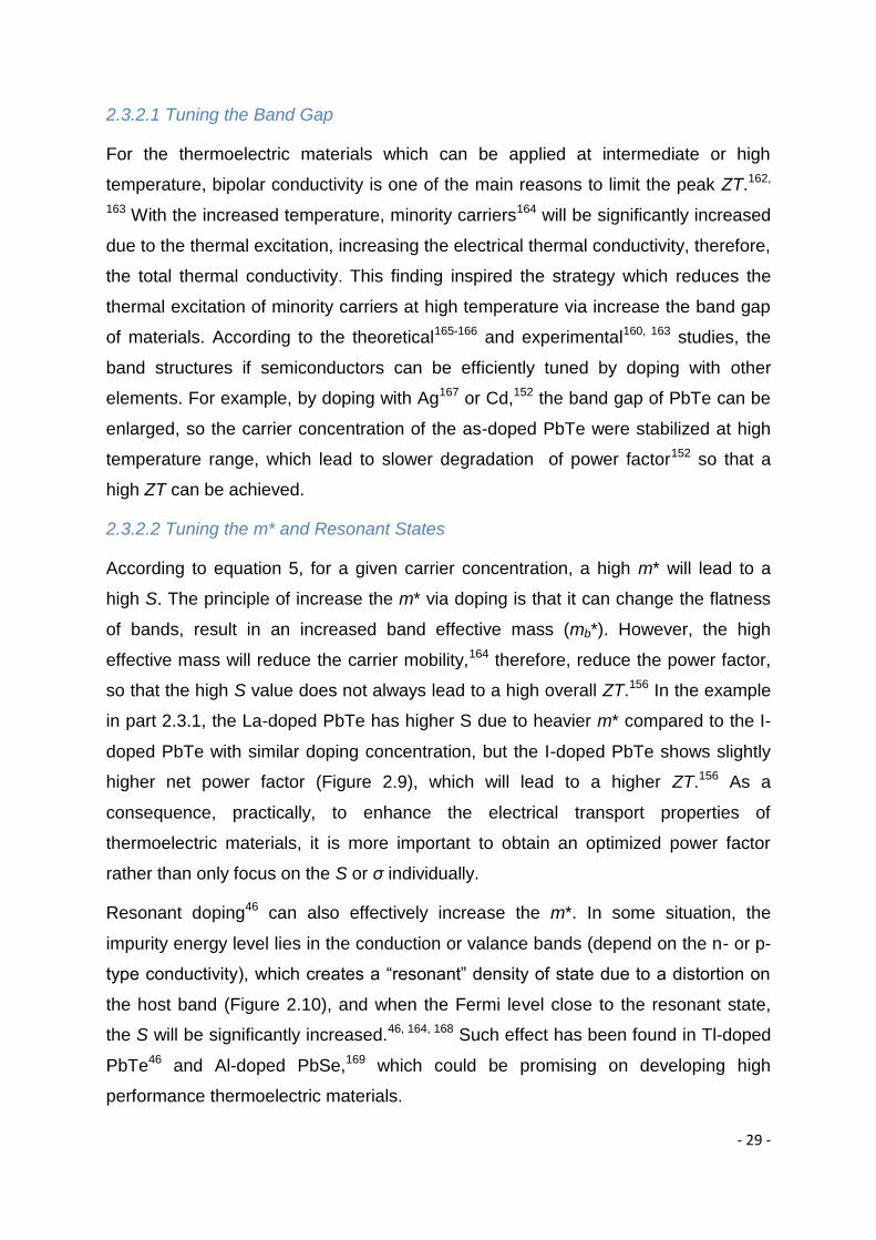
the host band (Figure 2.10), and when the Fermi level close to the resonant state,
the S will be significantly increased.46, 164, 168 Such effect has been found in Tl-doped
PbTe46 and Al-doped PbSe,169 which could be promising on developing high
performance thermoelectric materials.
Page 52
- 30 -
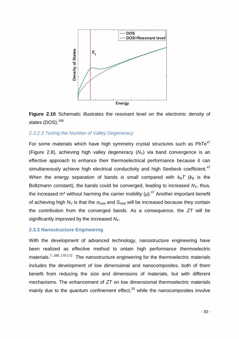
Figure 2.10 Schematic illustrates the resonant level on the electronic density of
states (DOS).168
2.3.2.3 Tuning the Number of Valley Degeneracy
For some materials which have high symmetry crystal structures such as PbTe47
(Figure 2.8), achieving high valley degeneracy (NV) via band convergence is an
effective approach to enhance their thermoelectrical performance because it can
simultaneously achieve high electrical conductivity and high Seebeck coefficient.47
When the energy separation of bands is small compared with kBT (kB is the
Boltzmann constant), the bands could be converged, leading to increased NV, thus,
the increased m* without harming the carrier mobility (μ).47 Another important benefit
of achieving high NV is that the σtotal and Stotal will be increased because they contain
the contribution from the converged bands. As a consequence, the ZT will be
significantly improved by the increased NV.
2.3.3 Nanostructure Engineering
With the development of advanced technology, nanostructure engineering have
been realized as effective method to ontain high performance thermoelectric
materials.7, 168, 170-172 The nanostructure engineering for the thermoelectric materials
includes the development of low dimensional and nanocomposites, both of them
benefit from reducing the size and dimensions of materials, but with different
mechanisms. The enhancement of ZT on low dimensiomal thermoelectric materials
mainly due to the quantum confinement effect,25 while the nanocomposites involve
Page 53
- 31 -
complex phonon scattering150 and low energy carrier filtering168 by the nano-scaled
substructures.
2.3.3.1 Low Dimensional Thermoelectric Materials
Nanostructures are defined as having one or more dimension between 1 and 100
nm.173 In 1993, Hicks and Dresselhaus25 suggested that low-dimensional or
nanocrystalline materials could achieve a high ZT due to the quantum size effect
which lead a higher density of states and a decreased lattice thermal conductivity
caused by the increase of phonon scattering.117, 174, 175 The dimensional decrease
causes the intensification of the quantum confinement as well as the decreasing
electron energy bands in nanostructure, which produce large Seebeck coefficient.
After that, a large number of theoretical calculations25, 17, 176, 177 and experimental
investigations26, 45, 178 have been done. High thermoelectric performance have been
extensively achieved in nanomaterials117 and a very high ZT are expected to be
obtained ultimately.
Remarkable enhancement of ZT of materials can be achieved through the
dimensionality decrease. In 2001, Venkatasubramanian117 reported the highest ZT
of ~2.4 in Bi2Te3/Sb2Te3 superlattice film, which boosted the thermoelectric property
compared to the bulk materials. Lin179 and Dresselhaus predicted that
heterostructure nanowires could have better thermoelectric performances than
superlattice films or conventional nanowires, which attract much attention to study
nanowires. However, the thermoelectric device based on this principle has not been
well-demonstrated yet.
2.3.3.2 Nanocomposites Thermoelectric Materials
Compared to nano-sized thermoelectric materials, nanocomposites174 materials are
easier to be fabricated and applied. Through appropriate procedures,150, 180-182 bulk
thermoelectric materials with nano-sized substructures can be synthesized. The
introduce of nanostructures into bulk materials will create high density of interfaces
(grain boundaries), lattice distortion and defects,172 which can significantly scatter
phonons which contribute to the lattice thermal conductivity, therefore, reduce the
thermal conductivity. Figure 2.11 shows the principle of how nanoparticles that
dispersed in bulk materials can scatter phonons with different wavelengths without
block the transport of electrons. The phonons with medium and long wavelength
Page 54
- 32 -
could be strongly scattered by the nano-sized grains, grain boundaries, while short
wavelength phonons can be scattered by the point defects (such as atomic defects).
Such strong scattering to the phonons can reduce the lattice thermal conductivity at
most 50% and lead to a 2-fold increase in ZT.183 Meanwhile, electrons which have
much shorter wavelength than phonon would not be scattered so strongly, which
means that the electric conductivity will not be significantly influenced by the
nanocomposites.
Figure 2.11 Schematic diagram of phonon scattering mechaism and electronic
transport within a thermalelectric material.177
Another advantage of nanocomposites materials is that the boundary between the
nano-participates and the host materials can filter lower-energy charge carriers due
to the existing of potential barrier.168 As it can be seen form equation 5, the S value
strongly related with the carrier behaviour. From figure 2.12, low-energy carriers
negatively contribute to the Seebeck coefficient, while the carriers have energy
between 0.05 and 0.1 eV contribute the most. When the carriers transport through
the boundary potential barrier between grains, lower-energy charge carriers will be
Page 55
- 33 -
filtered, therefore, the average carrier energy can be increased, and the |S| can be
increased as a consequence while the electrical conductivity will not be significantly
reduced.
Figure 2.12 Calculated results for n-type Si80Ge20 show how the carriers with
different energy contribute to the Seebeck coefficient.168
2. 4 Unsolved Issues and Opportunities
Due to the interesting physical and chemical properties, metal chalcogenides
materials are always considered as promising thermoelectric materials with huge
potential of wide application. With the increasing attention being paid, great efforts
have been made to improve the thermoelectric performance of metal chalcogenides-
based materials. The thermoelectric properties of Cu2Se, PbTe and Bi2Te3-based
materials have been significantly enhanced in last two decades, but there are some
issues have been left in which the opportunities can be addressed:
1. An efficient synthesis approach is required. For the requirement of the industrial
applications of thermoelectric materials, environmental friendly, high efficient and
low cost methods which can produce high-quality thermoelectric materials are
necessarily studied.
2. There is still a large gap of ZT value between the experimental results and
theoretical calculation, which means for all the current thermoelectric materials,
Page 56
- 34 -
improvement of ZT is possible. For example, the calculated value of Seebeck
coefficient of p-type Bi2Te3 is 313 µVK-1 at 300 K ,105 which is superior than any
existing experimental value. If the high Seebeck coefficient can be achieve while
the thermal conductivity of Bi2Te3 approaching its amorphous limit, the ZT could
reach a very high value.
3. The mechanism of improving the ZT of Cu2Se, PbTe and Bi2Te3-based
nanomaterials by nano engineering and doping can be further studied and
explained systemically.
The goal of this project is to understand thermoelectric materials from a scientific
view, establish my own systemic research to understand master the synthesis
methodology to obtain Cu2Se, PbTe and Bi2Te3-based nanomaterials, and improve
their thermoelectric performance via nanostructure engineering and doping.
2.5 Summary
This Chapter has generally introduced the background for the project, provided a
literature review on the thermoelectric effects, the development of thermoelectric
materials, and the development of some major metal chalcogenides thermoelectric
materials, namely, Cu2Se, Bi2Te3 and PbTe. Based on the detailed review, although
extensive studies have been done on metal chalcogenides-based thermoelectric
materials, there are still urgent desires to further improve their thermoelectric
performance and understand the mechanisms for commercializing applications.
Page 57
- 35 -
Reference:
1. Hochbaum, A. I.; Chen, R.; Delgado, R. D.; Liang, W.; Garnett, E. C.; Najarian,
M.; Majumdar, A.; Yang, P., Enhanced thermoelectric performance of rough silicon
nanowires. Nature 2008, 451, 163-168.
2. Koumoto, K.; Terasaki, I.; Funahashi, R., Complex oxide materials for
potential thermoelectric applications. Mrs. Bull. 2006, 31, 206-210.
3. Yang, J. H.; Caillat, T., Thermoelectric materials for space and automotive
power generation. Mrs. Bull. 2006, 31, 224-229.
4. Tritt, T. M.; Subramanian, M. A., Thermoelectric materials, phenomena, and
applications: A bird's eye view. Mrs. Bull. 2006, 31, 188-194.
5. Dresselhaus, M. S.; Chen, G.; Tang, M. Y.; Yang, R. G.; Lee, H.; Wang, D. Z.;
Ren, Z. F.; Fleurial, J. P.; Gogna, P., New directions for low-dimensional
thermoelectric materials. Adv. Mater. 2007, 19, 1043-1053.
6. Slack, G. A., CRCHandbook of Thermoelectrics. CRC: Boca Raton, 1995.
7. Chen, Z. G.; Han, G.; Yang, L.; Cheng, L.; Zou, J., Nanostructured
thermoelectric materials: Current research and future challenge. Prog. Nat. Sci. 2012,
22, 535-549.
8. Nolas, G. S.; Poon, J.; Kanatzidis, M., Recent developments in bulk
thermoelectric materials. Mrs. Bull. 2006, 31, 199-205.
9. Lan, Y. C.; Minnich, A. J.; Chen, G.; Ren, Z. F., Enhancement of
thermoelectric figure-of-merit by a bulk nanostructuring approach. Adv. Funct. Mater.
2010, 20, 357-376.
10. Rao, A. M.; Ji, X. H.; Tritt, T. M., Properties of nanostructured one-
dimensional and composite thermoelectric materials. Mrs. Bull. 2006, 31, 218-223.
11. Rowe, D. M. e., CRC Handbook of Thermoelectrics. CRC: Boca Raton,
1995.
12. Pollock, D. D., In Handbook of thermoelectrics, CRC Press LLC: 1995.
13. Goldsmid, H. J., In Handbook of Thermoelectrics, CRC Press LLC: 1995.
14. Deng, Y. G.; Liu, J., Recent advances in direct solar thermal power generation.
J. Renew. Sustain. Energy 2009, 1, 052701.
15. Rowe, D. M., Taylor & Francis Group: 2006.
Page 58
- 36 -
16. Cho, J. Y.; Lim, Y. S.; Choi, S. M.; Kim, K. H.; Seo, W. S.; Park, H. H.,
Thermoelectric properties of spark plasma-sintered In(4)Se(3)-In(4)Te(3). J. Electron.
Mater. 2011, 40, 1024-1028.
17. Wan, C. L.; Wang, Y. F.; Wang, N.; Norimatsu, W.; Kusunoki, M.; Koumoto, K.,
Development of novel thermoelectric materials by reduction of lattice thermal
conductivity. Sci. Technol. Adv. Mater. 2010, 11, 1-7.
18. Xie, Y.; Su, H. L.; Li, B.; Qian, Y. T., A direct solvothermal route to
nanocrystalline selenides at low temperature. Mater. Res. Bull. 2000, 35, 459-464.
19. Rhyee, J. S.; Lee, K. H.; Lee, S. M.; Cho, E.; Il Kim, S.; Lee, E.; Kwon, Y. S.;
Shim, J. H.; Kotliar, G., Peierls distortion as a route to high thermoelectric
performance in In4Se3-delta crystals. Nature 2009, 459, 965-968.
20. Zhou, M.; Li, J. F.; Kita, T., Nanostructured AgPbmSbTem+2 system bulk
materials with enhanced thermoelectric performance. J. Am. Chem. Soc. 2008, 130,
4527-4532.
21. Wang, W. Z.; Poudel, B.; Wang, D. Z.; Ren, Z. F., Synthesis of PbTe
nanoboxes using a solvothermal technique. Adv. Mater. 2005, 17, 2110-2114.
22. Bukala, M.; Sankowski, P.; Buczko, R.; Kacman, P., Crystal and electronic
structure of PbTe/CdTe nanostructures. Nanoscale Res. Lett. 2011, 6, 126.
23. Ruan, X. F.; Xiao, W. K., Preparation and thermoelectric properties of
SiO2/beta-Zn4Sb3 nanocomposite materials. J. Wuhan Univ. Technol. 2009, 24, 694-
697.
24. Yang, R. G.; Chen, G., Nanostructured thermoelectric materials: from
superlattices to nanocomposites. Materials Integration 2006. 18, 31–36.
25. Hicks, L. D.; Harman, T. C.; Dresselhaus, M. S., Use of quantum-well
superlattices to obtain a high figure of merit from nonconventional thermoelectric
materials. Appl. Phys. Lett. 1993, 63, 3230-3232.
26. Hicks, L. D.; Harman, T. C.; Sun, X.; Dresselhaus, M. S., Experimental study
of the effect of quantum-well structures on the thermoelectric figure of merit. Phys.
Rev. B 1996, 53, 10493-10496.
27. Bottner, H.; Chen, G.; Venkatasubramanian, R., Aspects of thin-film
superlattice thermoelectric materials, devices, and applications. Mrs Bull. 2006, 31,
211-217.
Page 59
- 37 -
28. Smith, G. E.; Wolfe, R., Themoelectric properties of bismuth-antimony alloys.
J. Appl. Phys. 1962, 33, 841-846.
29. Yim, W. M.; Amith, A., Bi-Sb alloys for mageto-thermoelectric and
thermomagnetic cooling. Solid State Electron. 1972, 15, 1141-1165.
30. Devaux, X.; Brochin, F.; Martin-Lopez, R.; Scherrer, H., Study of the
microstructure influence on the transport properties of Bi86.5Sb13.5 polycrystalline
alloy. J. Phys. Chem. Solids 2002, 63, 119-125.
31. Tritt, T. M., Thermoelectric materials - Holey and unholey semiconductors.
Science 1999, 283, 804-805.
32. Wolfe, R.; Smith, G. E., Effects of a magnetic field on the thermoelectric
properties of a bismuth-antimony alloy. Appl. Phys. Lett. 1962, 1, 5-7.
33. Zhao, L. D.; Zhang, B. P.; Li, J. F.; Zhou, M.; Liu, W. S., Preparation and
properties of Nano-SiC dispersed Bi2Te3 thermoelectric materials. Rare Metal Mat.
Eng. 2007, 36, 408-411.
34. Zhang, Y. H.; Zhu, T. J.; Tu, J. P.; Zhao, X. B., Flower-like nanostructure and
thermoelectric properties of hydrothermally synthesized La-containing Bi2Te3 based
alloys. Mater. Chem. Phys. 2007, 103, 484-488.
35. Zhao, Y.; Dyck, J. S.; Hernandez, B. M.; Burda, C., Improving thermoelectric
properties of chemically synthesized Bi2Te3-based nanocrystals by annealing. J.
Phys.Chem. C 2010, 114, 11607-11613.
36. Zhao, X. B.; Zhang, Y. H.; Ji, X. H., Solvothermal synthesis of nano-sized
LaxBi(2-x) Te3 thermoelectric powders. Inorg. Chem. Commun. 2004, 7, 386-388.
37. Zhao, X. B.; Ji, X. H.; Zhang, Y. H.; Zhu, T. J.; Tu, J. P.; Zhang, X. B., Bismuth
telluride nanotubes and the effects on the thermoelectric properties of nanotube-
containing nanocomposites. Appl. Phys. Lett. 2005, 86, 062111.
38. Menke, E. J.; Li, Q.; Penner, R. M., Bismuth telluride (Bi2Te3) nanowires
synthesized by cyclic electrodeposition/stripping coupled with step edge decoration.
Nano Lett. 2004, 4, 2009-2014.
39. Dresselhaus, M. S.; Lin, Y. M.; Rabin, O.; Dresselhaus, G., Bismuth
nanowires for thermoelectric applications. Microscale Therm. Eng. 2003, 7, 207-219.
40. Murphy, J. E.; Beard, M. C.; Norman, A. G.; Ahrenkiel, S. P.; Johnson, J. C.;
Yu, P. R.; Micic, O. I.; Ellingson, R. J.; Nozik, A. J., PbTe colloidal nanocrystals:
Page 60
- 38 -
Synthesis, characterization, and multiple exciton generation. J. Am. Chem. Soc.
2006, 128, 3241-3247.
41. Anderson, M. E.; Bharadwaya, S. S. N.; Schaak, R. E., Modified polyol
synthesis of bulk-scale nanostructured bismuth antimony telluride. J. Mater. Chem.
2010, 20, 8362-8367.
42. Pei, Y. Z.; Lensch-Falk, J.; Toberer, E. S.; Medlin, D. L.; Snyder, G. J., High
thermoelectric performance in pbte due to large nanoscale Ag2Te precipitates and
La doping. Adv. Funct. Mater. 2011, 21, 241-249.
43. Cui, J. L., Solvothermal route to the preparation of (PbTe)(1-x)(SnTe)(x) (x=0.5)
with nanocrystals. Mater. Lett. 2004, 58, 3222-3225.
44. Bozin, E. S.; Malliakas, C. D.; Souvatzis, P.; Proffen, T.; Spaldin, N. A.;
Kanatzidis, M. G.; Billinge, S. J. L., Entropically stabilized local dipole formation in
lead chalcogenides. Science 2010, 330, 1660-1663.
45. Harman, T. C.; Taylor, P. J.; Walsh, M. P.; LaForge, B. E., Quantum dot
superlattice thermoelectric materials and devices. Science 2002, 297, 2229-2232.
46. Heremans, J. P.; Jovovic, V.; Toberer, E. S.; Saramat, A.; Kurosaki, K.;
Charoenphakdee, A.; Yamanaka, S.; Snyder, G. J., Enhancement of thermoelectric
efficiency in PbTe by distortion of the electronic density of states. Science 2008, 321,
554-557.
47. Pei, Y. Z.; Shi, X. Y.; LaLonde, A.; Wang, H.; Chen, L. D.; Snyder, G. J.,
Convergence of electronic bands for high performance bulk thermoelectrics. Nature
2011, 473, 66-69.
48. Jiang, L.; Zhu, Y. J.; Cui, J. B., Nanostructures of metal tellurides (PbTe,
CdTe, CoTe2, Bi2Te3, and Cu7Te4) with various morphologies: a general
solvothermal synthesis and optical properties. Eur. J. Inorg. Chem. 2010, 3005-3011.
49. Bera, C.; Soulier, M.; Navone, C.; Roux, G.; Simon, J.; Volz, S.; Mingo, N.,
Thermoelectric properties of nanostructured Si1-xGex and potential for further
improvement. J. Appl. Phys. 2010, 108, 124306.
50. Gao, Y.; Marconnet, A. M.; Panzer, M. A.; LeBlanc, S.; Dogbe, S.; Ezzahri, Y.;
Shakouri, A.; Goodson, K. E., Nanostructured interfaces for thermoelectrics. J.
Electron. Mater. 2010, 39, 1456-1462.
Page 61
- 39 -
51. Mingo, N.; Hauser, D.; Kobayashi, N. P.; Plissonnier, M.; Shakouri, A.,
"Nanoparticle-in-alloy" approach to efficient thermoelectrics: silicides in SiGe. Nano
Lett. 2009, 9, 711-715.
52. Zhou, A. J.; Zhao, X. B.; Zhu, T. J.; Yang, S. H.; Dasgupta, T.; Stiewe, C.;
Hassdorf, R.; Mueller, E., Microstructure and thermoelectric properties of SiGe-
added higher manganese silicides. Mater. Chem. Phys. 2010, 124, 1001-1005.
53. Snyder, G. J.; Toberer, E. S., Complex thermoelectric materials. Nat. Mater.
2008, 7, 105-114.
54. Li, H.; Tang, X. F.; Su, X. L.; Zhang, Q. J., Preparation and thermoelectric
properties of high-performance Sb additional Yb0.2Co4Sb12+y bulk materials with
nanostructure. Appl. Phys. Lett. 2008, 92, 202114.
55. Li, H.; Tang, X. F.; Zhang, Q. J.; Uher, C., High performance InxCeyCo4Sb12
thermoelectric materials with in situ forming nanostructured InSb phase. Appl. Phys.
Lett. 2009, 94, 102114.
56. Mi, J. L.; Zhao, X. B.; Zhu, T. J.; Tu, J. P., Improved thermoelectric figure of
merit in n-type CoSb3 based nanocomposites. Appl. Phys. Lett. 2008, 92, 029905.
57. Yim, W. M.; Rosi, F. D., Compound tellurides and their alloys for Peltier
cooling-Review. Solid State Electron. 1972, 15, 1121-1140.
58. Chung, D. Y.; Hogan, T.; Brazis, P.; Rocci-Lane, M.; Kannewurf, C.; Bastea,
M.; Uher, C.; Kanatzidis, M. G., CsBi4Te6: A high-performance thermoelectric
material for low-temperature applications. Science 2000, 287, 1024-1027.
59. Walther, D. C.; Ahn, J., Advances and challenges in the development of
power-generation systems at small scales. Prog. Energ. Combust. 2011, 37, 583-
610.
60. Poudeu, P. F. P.; D'Angelo, J.; Kong, H. J.; Downey, A.; Short, J. L.; Pcionek,
R.; Hogan, T. P.; Uher, C.; Kanatzidis, M. G., Nanostructures versus solid solutions:
Low lattice thermal conductivity and enhanced thermoelectric figure of merit in
Pb9.6Sb0.2Te10-xSex bulk materials. J. Am. Chem. Soc. 2006, 128, 14347-14355.
61. Poudeu, P. F. R.; D'Angelo, J.; Downey, A. D.; Short, J. L.; Hogan, T. P.;
Kanatzidis, M. G., High thermoelectric figure of merit and nanostructuring in bulk p-
type Na1-xPbmSbyTem+2. Angew. Chem. Int. Edit. 2006, 45, 3835-3839.
62. Wu, Y. Y.; Fan, R.; Yang, P. D., Block-by-block growth of single-crystalline
Si/SiGe superlattice nanowires. Nano Lett. 2002, 2, 83-86.
Page 62
- 40 -
63. Wu, J.; Yang, J. Y.; Zhang, H.; Zhang, J. S.; Feng, S. L.; Liu, M.; Peng, J. Y.;
Zhu, W.; Zou, T., Fabrication of Ag-Sn-Sb-Te based thermoelectric materials by MA-
PAS and their properties. J. Alloy. Compd. 2010, 507, 167-171.
64. Yang, S. H.; Zhu, T. J.; Sun, T.; Zhang, S. N.; Zhao, X. B.; He, J.,
Nanostructures in high-performance (GeTe)(x)(AgSbTe2)(100-x) thermoelectric
materials. Nanotechnology 2008, 19, 245707.
65. Sun, J. H.; Qin, X. Y.; Xin, H. X.; Li, D.; Pan, L.; Song, C. J.; Zhang, J.; Sun, R.
R.; Wang, Q. Q.; Liu, Y. F., Synthesis and thermoelectric properties of
Zn4Sb3/Bi0.5Sb1.5Te3 bulk nanocomposites. J. Alloy. Compd. 2010, 500, 215-219.
66. Wang, Y.; Fan, H. J., Improved thermoelectric properties of La1−xSrxCoO3
nanowires. J. Phys. Chem. C 2010, 114, 13947-13953.
67. Terasaki, I.; Sasago, Y.; Uchinokura, K., Large thermoelectric power in
NaCo2O4 single crystals. Phys. Rev. B 1997, 56, 12685-12687.
68. Hsu, K. F.; Loo, S.; Guo, F.; Chen, W.; Dyck, J. S.; Uher, C.; Hogan, T.;
Polychroniadis, E. K.; Kanatzidis, M. G., Cubic AgPbmSbTe2+m: Bulk thermoelectric
materials with high figure of merit. Science 2004, 303, 818-821.
69. Han, G.; Chen, Z.-G.; Yang, L.; Hong, M.; Drennan, J.; Zou, J., Rational
design of Bi2Te3 polycrystalline whiskers for thermoelectric applications. ACS Appl.
Mat. Interfaces 2014, 7, 989-995.
70. Riha, S. C.; Johnson, D. C.; Prieto, A. L., Cu2Se nanoparticles with tunable
electronic properties due to a controlled solid-state phase transition driven by copper
oxidation and cationic conduction. J. Am. Chem. Soc. 2010, 133, 1383-1390.
71. Liu, H.; Shi, X.; Xu, F.; Zhang, L.; Zhang, W.; Chen, L.; Li, Q.; Uher, C.; Day,
T.; Snyder, G. J., Copper ion liquid-like thermoelectrics. Nat. Mater. 2012, 11, 422-
425.
72. Brown, D. R.; Day, T.; Borup, K. A.; Christensen, S.; Iversen, B. B.; Snyder, G.
J., Phase transition enhanced thermoelectric figure-of-merit in copper chalcogenides.
APL Mater. 2013, 1, 052107.
73. Liu, H.; Yuan, X.; Lu, P.; Shi, X.; Xu, F.; He, Y.; Tang, Y.; Bai, S.; Zhang, W.;
Chen, L.; Lin, Y.; Shi, L.; Lin, H.; Gao, X.; Zhang, X.; Chi, H.; Uher, C., Ultrahigh
thermoelectric performance by electron and phonon critical scattering in Cu2Se1-xIx.
Adv. Mater. 2013, 25, 6607-6612.
Page 63
- 41 -
74. Su, X.; Fu, F.; Yan, Y.; Zheng, G.; Liang, T.; Zhang, Q.; Cheng, X.; Yang, D.;
Chi, H.; Tang, X.; Zhang, Q.; Uher, C., Self-propagating high-temperature synthesis
for compound thermoelectrics and new criterion for combustion processing. Nat.
Commun. 2014, 5. 4908.
75. Liu, H.; Shi, X.; Kirkham, M.; Wang, H.; Li, Q.; Uher, C.; Zhang, W.; Chen, L.,
Structure-transformation-induced abnormal thermoelectric properties in
semiconductor copper selenide. Mater. Lett. 2013, 93, 121-124.
76. He, Y.; Day, T.; Zhang, T.; Liu, H.; Shi, X.; Chen, L.; Snyder, G. J., High
thermoelectric performance in non-toxic earth-abundant copper sulfide. Adv. Mater.
2014, 26, 3974-3978.
77. Tyagi, K.; Gahtori, B.; Bathula, S.; Jayasimhadri, M.; Sharma, S.; Singh, N. K.;
Haranath, D.; Srivastava, A. K.; Dhar, A., Crystal structure and mechanical
properties of spark plasma sintered Cu2Se: An efficient photovoltaic and
thermoelectric material. Solid State Commun. 2015, 207, 21-25.
78. Yang, L.; Chen, Z.-G.; Han, G.; Hong, M.; Zou, Y.; Zou, J., High-performance
thermoelectric Cu2Se nanoplates through nanostructure engineering. Nano Energy
2015, 16, 367-374.
79. Zhao, Y.; Zhu, L.; Jiang, Y.; Xie, H.; Zhang, G.; Ba, N., Microphone shaped
Cu2Se micro/nano architecture: Preparation, formation mechanism and optical
property. Mater. Lett. 2015, 147, 82-84.
80. Xu, J.; Zhang, W.; Yang, Z.; Ding, S.; Zeng, C.; Chen, L.; Wang, Q.; Yang, S.,
Large-Scale Synthesis of Long Crystalline Cu2-xSe Nanowire Bundles by Water-
Evaporation-Induced Self-Assembly and Their Application in Gas Sensing. Adv.
Funct. Mater. 2009, 19, 1759-1766.
81. Yue, J.-L.; Sun, Q.; Fu, Z.-W., Cu2Se with facile synthesis as a cathode
material for rechargeable sodium batteries. Chem. Commun. 2013, 49, 5868-5870.
82. Mahan, G. D., The Seebeck coefficient of superionic conductors. J. Appl.
Phys. 2015, 117. 045101.
83. Lubomir, G.; Marek, D.; Oksana, S.; Adam, P., Crystal structure of Cu2Se.
Chem.Metals and Alloys 2011,4. 200-205.
84. Tonejc, A.; Tonejc, A. M., X-ray diffraction study on α ↔ β phase transition of
Cu2Se. J. Solid State Chem. 1981, 39, 259-261.
Page 64
- 42 -
85. Glazov, V. M.; Pashinkin, A. S.; Fedorov, V. A., Phase equilibria in the Cu-Se
system. Inorg. Mater. 2000, 36, 641-652.
86. Jia, F.; Zhang, S.; Zhang, X.; Peng, X.; Zhang, H.; Xiang, Y., Sb-triggered β-
to-α transition: solvothermal synthesis of metastable α-Cu2Se. Chem.Euro. J. 2014,
20, 15941-15946.
87. Danilkin, S. A.; Skomorokhov, A. N.; Hoser, A.; Fuess, H.; Rajevac, V.;
Bickulova, N. N., Crystal structure and lattice dynamics of superionic copper selenide
Cu2−δSe. J. Alloy Compd 2003, 361, 57-61.
88. Ohtani, T.; Tachibana, Y.; Ogura, J.; Miyake, T.; Okada, Y.; Yokota, Y.,
Physical properties and phase transitions of β Cu2−xSe (0.20≤x≤0.25). J. Alloy
Compd 1998, 279, 136-141.
89. Skomorokhov, A. N.; Trots, D. M.; Knapp, M.; Bickulova, N. N.; Fuess, H.,
Structural behaviour of β-Cu2−δSe (δ = 0, 0.15, 0.25) in dependence on temperature
studied by synchrotron powder diffraction. J. Alloy Compd 2006, 421, 64-71.
90. Tonejc, A.; Ogorelec, Z.; Mestnik, B., X-ray investigation of copper selenides
Cu2-xSe (2.00>=2-x>=1.72). J. Appl. Crystallogr. 1975, 8, 375-379.
91. Zhao, L.; Wang, X.; Yun, F. F.; Wang, J.; Cheng, Z.; Dou, S.; Wang, J.;
Snyder, G. J., The effects of Te2− and I− substitutions on the electronic structures,
thermoelectric performance, and hardness in melt-quenched highly dense Cu2-xSe.
Adv. Electron. Mater. 2015, 1, 1400015.
92. Tyagi, K.; Gahtori, B.; Bathula, S.; Jayasimhadri, M.; Singh, N. K.; Sharma, S.;
Haranath, D.; Srivastava, A. K.; Dhar, A., Enhanced thermoelectric performance of
spark plasma sintered copper-deficient nanostructured copper selenide. J. Phys.
Chem. Solids 2015, 81, 100-105.
93. Lesnyak, V.; Brescia, R.; Messina, G. C.; Manna, L., Cu vacancies boost
cation exchange reactions in copper selenide nanocrystals. J. Am. Chem. Soc. 2015,
137, 9315-9323.
94. Callaway, J.; von Baeyer, H. C., Effect of point imperfections on lattice
thermal conductivity. Phys. Rev. 1960, 120, 1149-1154.
95. Kim, H.; Ballikaya, S.; Chi, H.; Ahn, J.-P.; Ahn, K.; Uher, C.; Kaviany, M.,
Ultralow thermal conductivity of -Cu2Se by atomic fluidity and structure distortion.
Acta Mater. 2015, 86, 247-253.
Page 65
- 43 -
96. Kim, J. H.; Oh, S.; Sohn, W. H.; Rhyee, J.-S.; Park, S.-D.; Kang, H.; Ahn, D.,
Thermoelectric, thermodynamic, and structural properties in Cu(1.94)A(0.02)Se (A = Al,
Ga, and In) polycrystalline compounds. Acta Mater. 2015, 100, 32-38.
97. Ballikaya, S.; Chi, H.; Salvador, J. R.; Uher, C., Thermoelectric properties of
Ag-doped Cu2Se and Cu2Te. J. Mater. Chem. A 2013, 1, 12478-12484.
98. Hu, H.; Ge, X.; Deng, C.; Sun, M.; Xuan, H.; Zhang, K., Copper Selenide
(CuSe and Cu2Se) nanocrystals: controllable synthesis through a facile ultrasonic
chemical route. Asian J. Chem. 2013, 25, 5516-5518.
99. Liu, S.; Zhang, Z.; Bao, J.; Lan, Y.; Tu, W.; Han, M.; Dai, Z., Controllable
synthesis of tetragonal and cubic phase Cu2Se nanowires assembled by small
nanocubes and their electrocatalytic performance for oxygen reduction reaction. J.
Phys.Chem. C 2013, 117, 15164-15173.
100. Li, D.; Qin, X. Y.; Liu, Y. F.; Song, C. J.; Wang, L.; Zhang, J.; Xin, H. X.; Guo,
G. L.; Zou, T. H.; Sun, G. L.; Ren, B. J.; Zhu, X. G., Chemical synthesis of
nanostructured Cu2Se with high thermoelectric performance. Rsc Adv. 2014, 4,
8638-8644.
101. Zhong, B.; Zhang, Y.; Li, W.; Chen, Z.; Cui, J.; Li, W.; Xie, Y.; Hao, Q.; He, Q.,
High superionic conduction arising from aligned large lamellae and large figure of
merit in bulk Cu1.94Al0.02Se. Appl. Phys. Lett. 2014, 105.
102. Scherrer, S.; Scherrer, H., Thermoelectrics Handbook, CRC Press: 2005;
pp 27-1-27-19.
103. Greenawa.Dl; Harbeke, G., Band structure of bismuth telluride bismuth
selenide and their respective alloys. J. Phys. Chem. Solids 1965, 26, 1585-1604.
104. Sootsman, J. R.; Chung, D. Y.; Kanatzidis, M. G., New and old concepts in
thermoelectric materials. Angew. Chem. Int. Edit. 2009, 48, 8616-8639.
105. Mishra, S. K.; Satpathy, S.; Jepsen, O., Electronic structure and
thermoelectric properties of bismuth telluride and bismuth selenide. J. Phys-condens
Mat. 1997, 9, 461-470.
106. Poudel, B.; Hao, Q.; Ma, Y.; Lan, Y. C.; Minnich, A.; Yu, B.; Yan, X.; Wang, D.
Z.; Muto, A.; Vashaee, D.; Chen, X. Y.; Liu, J. M.; Dresselhaus, M. S.; Chen, G.; Ren,
Z., High-thermoelectric performance of nanostructured bismuth antimony telluride
bulk alloys. Science 2008, 320, 634-638.
Page 66
- 44 -
107. Xie, W.; Tang, X.; Yan, Y.; Zhang, Q.; Tritt, T. M., High thermoelectric
performance BiSbTe alloy with unique low-dimensional structure. J. Appl. Phys.
2009, 105.
108. Fan, S.; Zhao, J.; Guo, J.; Yan, Q.; Ma, J.; Hng, H. H., p-type Bi0.4Sb1.6Te3
nanocomposites with enhanced figure of merit. Appl. Phys. Lett. 2010, 96, 182104.
109. Yan, X.; Poudel, B.; Ma, Y.; Liu, W. S.; Joshi, G.; Wang, H.; Lan, Y.; Wang, D.;
Chen, G.; Ren, Z. F., Experimental studies on anisotropic thermoelectric properties
and structures of n-type Bi2Te2.7Se0.3. Nano Lett. 2010, 10, 3373-3378.
110. Liu, W.-S.; Zhang, Q.; Lan, Y.; Chen, S.; Yan, X.; Zhang, Q.; Wang, H.; Wang,
D.; Chen, G.; Ren, Z., Thermoelectric property studies on Cu-doped n-type
CuxBi2Te2.7Se0.3 nanocomposites. Adv. Energy Mater. 2011, 1, 577-587.
111. Zhang, G.; Kirk, B.; Jauregui, L. A.; Yang, H.; Xu, X.; Chen, Y. P.; Wu, Y.,
Rational synthesis of ultrathin n-Type Bi2Te3 nanowires with enhanced
thermoelectric properties. Nano Lett. 2012, 12, 56-60.
112. Zhang, G.; Fang, H.; Yang, H.; Jauregui, L. A.; Chen, Y. P.; Wu, Y., Design
principle of telluride-based nanowire heterostructures for potential thermoelectric
applications. Nano Letters 2012, 12, 3627-3633.
113. Soni, A.; Zhao, Y. Y.; Yu, L. G.; Aik, M. K. K.; Dresselhaus, M. S.; Xiong, Q.
H., Enhanced thermoelectric properties of solution grown Bi2Te3-xSex nanoplatelet
composites. Nano Lett. 2012, 12, 1203-1209.
114. Son, J. S.; Choi, M. K.; Han, M. K.; Park, K.; Kim, J. Y.; Lim, S. J.; Oh, M.;
Kuk, Y.; Park, C.; Kim, S. J.; Hyeon, T., n-Type nanostructured thermoelectric
materials prepared from chemically synthesized ultrathin Bi2Te3 nanoplates. Nano
Lett. 2012, 12, 640-647.
115. Mehta, R. J.; Zhang, Y. L.; Karthik, C.; Singh, B.; Siegel, R. W.; Borca-Tasciuc,
T.; Ramanath, G., A new class of doped nanobulk high-figure-of-merit
thermoelectrics by scalable bottom-up assembly. Nat. Mater. 2012, 11, 233-240.
116. Xie, W.; Tang, X.; Yan, Y.; Zhang, Q.; Tritt, T. M., Unique nanostructures and
enhanced thermoelectric performance of melt-spun BiSbTe alloys. Appl. Phys. Lett.
2009, 94, 102111.
117. Venkatasubramanian, R.; Siivola, E.; Colpitts, T.; O'Quinn, B., Thin-film
thermoelectric devices with high room-temperature figures of merit. Nature 2001,
413, 597-602.
Page 67
- 45 -
118. Dziawa, P.; Sadowski, J.; Dluzewski, P.; Lusakowska, E.; Domukhovski, V.;
Taliashvili, B.; Wojciechowski, T.; Baczewski, L. T.; Bukala, M.; Galicka, M.; Buczko,
R.; Kacman, P.; Story, T., Defect free PbTe nanowires grown by molecular beam
epitaxy on GaAs(111)B substrates. Cryst. Growth Des. 2010, 10, 109-113.
119. Ni, Y. H.; Zhang, Y. M.; Hong, J. M., Thicket-like PbTe microstructures built up
of plentiful nanoflakes: a facile preparation, characterization and influencing factors.
Crystengcomm 2011, 13, 1910-1915.
120. DiSalvo, F. J., Thermoelectric cooling and power generation. Science 1999,
285, 703-706.
121. Pei, Y.; Wang, H.; Snyder, G. J., Band engineering of thermoelectric materials.
Adv. Mater. 2012, 24, 6125-35.
122. LaLonde, A. D.; Pei, Y.; Wang, H.; Snyder, G. J., Lead telluride alloy
thermoelectrics. Mater. Today 2011, 14, 526-532.
123. Fritts, R. W., Thermoelectric Materials and Devices. Reinhold Publishing
Corporation: New York, 1960.
124. Zhang, Q.; Wang, H.; Zhang, Q.; Liu, W.; Yu, B.; Wang, H.; Wang, D.; Ni, G.;
Chen, G.; Ren, Z., Effect of silicon and sodium on thermoelectric properties of
thallium-doped lead telluride-based materials. Nano Lett. 2012, 12, 2324-2330.
125. Pei, Y.; LaLonde, A.; Iwanaga, S.; Snyder, G. J., High thermoelectric figure of
merit in heavy hole dominated PbTe. Energy Environ. Sci. 2011, 4, 2085-2089.
126. LaLonde, A. D.; Pei, Y.; Snyder, G. J., Reevaluation of PbTe(1-x)I(x) as high
performance n-type thermoelectric material. Energy Environ. Sci. 2011, 4, 2090-
2096.
127. Pei, Y.; Shi, X.; LaLonde, A.; Wang, H.; Chen, L.; Snyder, G. J., Convergence
of electronic bands for high performance bulk thermoelectrics. Nature 2011, 473, 66-
69.
128. Tauber, R. N.; Machonis, A. A.; Cadoff, I. B., Thermal and Optical Energy
Gaps in PbTe. J. Appl. Phys. 1966, 37, 4855-4860.
129. Sitter, H.; Lischka, K.; Heinrich, H., Structure of the second valence band in
PbTe. Phys. Rev. B 1977, 16, 680-687.
130. Bilc, D.; Mahanti, S. D.; Quarez, E.; Hsu, K.-F.; Pcionek, R.; Kanatzidis, M. G.,
Resonant states in the electronic structure of the high performance thermoelectrics
Page 68
- 46 -
AgPbmSbTe2+m: the role of Ag-Sb microstructures. Phys. Revi. Lett. 2004, 93,
146403.
131. Nimtz, G.; Schlicht, B., Narrow-gap lead salts. Springer Tracts in Modern
Phys. 1983, 98, 1-117.
132. Zou, G. F.; Liu, Z. P.; Wang, D. B.; Jiang, C. L.; Qian, Y. T., Selected-control
solvothermal synthesis of nanoscale hollow spheres and single-crystal tubes of PbTe.
Eur. J. Inorg. Chem. 2004, 4521-4524.
133. Roh, J. W.; Jang, S. Y.; Kang, J.; Lee, S.; Noh, J. S.; Kim, W.; Park, J.; Lee,
W., Size-dependent thermal conductivity of individual single-crystalline PbTe
nanowires. Appl. Phys. Lett. 2010, 96, 103101.
134. Chen, X.; Zhu, T. J.; Zhao, X. B., Controllable synthesis of PbTe nanosheets
via an alkaline hydrothermal method. Inec: 2010 3rd International Nanoelectronics
Conference, Vols 1 and 2 2010, 1179-1180.
135. Zhu, T. J.; Chen, X.; Meng, X. Y.; Zhao, X. B.; He, J., Anisotropic growth of
cubic PbTe nanoparticles to nanosheets: controlled synthesis and growth
mechanisms. Crys.Growth Des. 2010, 10, 3727-3731.
136. Qiu, X. F.; Lou, Y. B.; Samia, A. C. S.; Devadoss, A.; Burgess, J. D.; Dayal, S.;
Burda, C., PbTe nanorods by sonoelectrochemistry. Angew. Chem. Int. Edit. 2005,
44, 5855-5857.
137. Wang, Y. Y.; Cai, K. F.; Yao, X., Facile Fabrication and thermoelectric
properties of PbTe-modified poly(3,4-ethylenedioxythiophene) nanotubes. ACS Appl.
Mat. Interfaces 2011, 3, 1163-1166.
138. Lv, W. Z.; Weng, W. J., Synthesis and characterization of PbTe nanoparticles
under ultrasonic/microwave co-irradiation. 2009 Asia-Pacific Power and Energy
Engineering Conference (Appeec), Vols 1-7 2009, 645-647.
139. Jin, R. C.; Chen, G.; Wang, Q.; Pei, J. A.; Sun, J. X.; Wang, Y., PbTe
hierarchical nanostructures: solvothermal synthesis, growth mechanism and their
electrical conductivities. Crystengcomm 2011, 13, 2106-2113.
140. Zhang, B.; He, J.; Tritt, T. M., Size-selective high-yield growth of lead telluride
(PbTe) nanocrystals using a chemical vapor deposition technique. Appl. Phys. Lett.
2006, 88, 043119.
141. Zhang, B.; Gothard, N.; He, J.; Thompson, D.; Tritt, T. M., Size-selective and
high-yield nanocrystal growth of PbTe compounds using a chemical vapor deposition
Page 69
- 47 -
technique. Materials and Technologies for Direct Thermal-to-Electric Energy
Conversion 2006, 886, 169-174.
142. Zong, Z. C.; Zhang, M. Z.; Lu, H. L.; Xu, D.; Wang, S. M.; Tian, H. F.; Liu, C.;
Guo, H. M.; Gao, H. J.; Zou, G. T., Synthesis of PbTe/Pb quasi-one-dimensional
nanostructure material arrays by electrodeposition. Appl. Phys. Lett. 2010, 96,
143113.
143. Ni, Y. H.; Qiu, B.; Hong, J. M.; Zhang, L.; Wei, X. W., Hydrothermal synthesis,
characterization, and influence factors of PbTe nanocrystals. Mater. Res. Bull. 2008,
43, 2668-2676.
144. Wan, B. Y.; Hu, C. G.; Feng, B.; Xi, Y.; He, X. S., Synthesis and
thermoelectric properties of PbTe nanorods and microcubes. Mater. Sci. Eng. B-Adv.
2009, 163, 57-61.
145. Wu, D.; Zhao, L.-D.; Tong, X.; Li, W.; Wu, L.; Tan, Q.; Pei, Y.; Huang, L.; Li,
J.-F.; Zhu, Y.; Kanatzidis, M. G.; He, J., Superior thermoelectric performance in
PbTe-PbS pseudo-binary: extremely low thermal conductivity and modulated carrier
concentration. Energy Environ. Sci. 2015, 8, 2056-2068.
146. Ahn, K.; Han, M. K.; He, J. Q.; Androulakis, J.; Ballikaya, S.; Uher, C.; Dravid,
V. P.; Kanatzidis, M. G., Exploring resonance levels and nanostructuring in the
PbTe-CdTe system and enhancement of the thermoelectric figure of merit. J. Am.
Chem. Soc. 2010, 132, 5227-5235.
147. Androulakis, J.; Hsu, K. F.; Pcionek, R.; Kong, H.; Uher, C.; Dangelo, J. J.;
Downey, A.; Hogan, T.; Kanatzidis, M. G., Nanostructuring and high thermoelectric
efficiency in p-type Ag(Pb1-ySny)(m)SbTe2+m. Adv. Mater. 2006, 18, 1170-1173.
148. Androulakis, J.; Lin, C. H.; Kong, H. J.; Uher, C.; Wu, C. I.; Hogan, T.; Cook, B.
A.; Caillat, T.; Paraskevopoulos, K. M.; Kanatzidis, M. G., Spinodal decomposition
and nucleation and growth as a means to bulk nanostructured thermoelectrics:
Enhanced performance in Pb1-xSnxTe-PbS. J. Am. Chem. Soc. 2007, 129, 9780-
9788.
149. Pei, Y.; Heinz, N. A.; LaLonde, A.; Snyder, G. J., Combination of large
nanostructures and complex band structure for high performance thermoelectric lead
telluride. Energy Environ. Sci. 2011, 4, 3640-3645.
Page 70
- 48 -
150. Biswas, K.; He, J.; Blum, I. D.; Wu, C.-I.; Hogan, T. P.; Seidman, D. N.; Dravid,
V. P.; Kanatzidis, M. G., High-performance bulk thermoelectrics with all-scale
hierarchical architectures. Nature 2012, 489, 414-8.
151. Biswas, K.; He, J.; Zhang, Q.; Wang, G.; Uher, C.; Dravid, V. P.; Kanatzidis,
M. G., Strained endotaxial nanostructures with high thermoelectric figure of merit.
Nat. Chem. 2011, 3, 160-166.
152. Pei, Y.; LaLonde, A. D.; Heinz, N. A.; Snyder, G. J., High thermoelectric figure
of merit in PbTe alloys demonstrated in PbTe-CdTe. Adv. Energy Mater. 2012, 2,
670-675.
153. Wu, H. J.; Zhao, L. D.; Zheng, F. S.; Wu, D.; Pei, Y. L.; Tong, X.; Kanatzidis,
M. G.; He, J. Q., Broad temperature plateau for thermoelectric figure of merit ZT > 2
in phase-separated PbTe0.7S0.3. Nat. Commun. 2014, 5.
154. Pei, Y.; LaLonde, A. D.; Heinz, N. A.; Shi, X.; Iwanaga, S.; Wang, H.; Chen, L.;
Snyder, G. J., Stabilizing the optimal carrier concentration for high thermoelectric
efficiency. Adv. Mater. 2011, 23, 5674-5678.
155. Slack, G. A., CRC Handbook of Thermoelectrics. 1995; pp 407-440.
156. Pei, Y.; Gibbs, Z. M.; Gloskovskii, A.; Balke, B.; Zeier, W. G.; Snyder, G. J.,
Optimum carrier concentration in n-Type PbTe thermoelectrics. Adv. Energy Mater.
2014, 4, 486-486.
157. Ioffe, A. F., Semiconductor thermoelements, and Thermoelectric cooling.
Infosearch, ltd.: 1957.
158. Goncalves, L. M.; Couto, C.; Alpuim, P.; Rolo, A. G.; Völklein, F.; Correia, J.
H., Optimization of thermoelectric properties on Bi2Te3 thin films deposited by
thermal co-evaporation. Thin Solid Films 2010, 518, 2816-2821.
159. Chasapis, T. C.; Lee, Y.; Hatzikraniotis, E.; Paraskevopoulos, K. M.; Chi, H.;
Uher, C.; Kanatzidis, M. G., Understanding the role and interplay of heavy-hole and
light-hole valence bands in the thermoelectric properties of PbSe. Phys. Rev. B
2015, 91, 085207.
160. Pei, Y. Z.; Heinz, N. A.; Snyder, G. J., Alloying to increase the band gap for
improving thermoelectric properties of Ag2Te. J. Mater. Chem. 2011, 21, 18256-
18260.
161. Pei, Y.; LaLonde, A. D.; Wang, H.; Snyder, G. J., Low effective mass leading
to high thermoelectric performance. Energy Environ. Sci. 2012, 5, 7963-7969.
Page 71
- 49 -
162. Bahk, J.-H.; Shakouri, A., Enhancing the thermoelectric figure of merit through
the reduction of bipolar thermal conductivity with heterostructure barriers. Appl. Phys.
Lett. 2014, 105.
163. Zhao, L. D.; Wu, H. J.; Hao, S. Q.; Wu, C. I.; Zhou, X. Y.; Biswas, K.; He, J. Q.;
Hogan, T. P.; Uher, C.; Wolverton, C.; Dravid, V. P.; Kanatzidis, M. G., All-scale
hierarchical thermoelectrics: MgTe in PbTe facilitates valence band convergence
and suppresses bipolar thermal transport for high performance. Energy Environ. Sci.
2013, 6, 3346-3355.
164. Pei, Y.; Wang, H.; Snyder, G. J., Band engineering of thermoelectric materials.
Adv. Mater. 2012, 24, 6125-35.
165. Boukhris, N.; Meradji, H.; Ghemid, S.; Drablia, S.; Hassan, F. E., Ab initio
study of the structural, electronic and thermodynamic properties of PbSe1-xSx,
PbSe1-xTex and PbS1-xTex ternary alloys. Phys. Scripta 2011, 83.
166. Hoang, K.; Mahanti, S. D.; Kanatzidis, M. G., Impurity clustering and impurity-
induced bands in PbTe-, SnTe-, and GeTe-based bulk thermoelectrics. Phys. Rev. B
2010, 81.
167. Pei, Y.; May, A. F.; Snyder, G. J., Self-tuning the carrier concentration of
PbTe/Ag2Te composites with excess Ag for high thermoelectric performance. Adv.
Energy Mater. 2011, 1, 291-296.
168. Minnich, A. J.; Dresselhaus, M. S.; Ren, Z. F.; Chen, G., Bulk nanostructured
thermoelectric materials: current research and future prospects. Energy Environ Sci
2009, 2, 466-479.
169. Zhang, Q.; Wang, H.; Liu, W.; Wang, H.; Yu, B.; Zhang, Q.; Tian, Z.; Ni, G.;
Lee, S.; Esfarjani, K.; Chen, G.; Ren, Z., Enhancement of thermoelectric figure-of-
merit by resonant states of aluminium doping in lead selenide. Energy Environ. Sci.
2012, 5, 5246-5251.
170. Boukai, A. I.; Bunimovich, Y.; Tahir-Kheli, J.; Yu, J.-K.; Goddard, W. A., III;
Heath, J. R., Silicon nanowires as efficient thermoelectric materials. Nature 2008,
451, 168-171.
171. Heremans, J. P.; Dresselhaus, M. S.; Bell, L. E.; Morelli, D. T., When
thermoelectrics reached the nanoscale. Nat. Nano. 2013, 8, 471-473.
172. Kim, W.; Wang, R.; Majumdar, A., Nanostructuring expands thermal limits.
Nano Today 2007, 2, 40-47.
Page 72
- 50 -
173. Xia, Y. N.; Yang, P. D.; Sun, Y. G.; Wu, Y. Y.; Mayers, B.; Gates, B.; Yin, Y.
D.; Kim, F.; Yan, Y. Q., One-dimensional nanostructures: Synthesis, characterization,
and applications. Adv. Mater. 2003, 15, 353-389.
174. Fan, X. A.; Yang, J. Y.; Xie, Z.; Li, K.; Zhu, W.; Duan, X. K.; Xiao, C. J.; Zhang,
Q. Q., Bi2Te3 hexagonal nanoplates and thermoelectric properties of n-type Bi2Te3
nanocomposites. J. Phys. D Appl. Phys. 2007, 40, 5975-5979.
175. Lu, W. G.; Ding, Y.; Chen, Y. X.; Wang, Z. L.; Fang, J. Y., Bismuth telluride
hexagonal nanoplatelets and their two-step epitaxial growth. J. Am. Chem. Soc.
2005, 127, 10112-10116.
176. Pichanusakorn, P.; Bandaru, P., Nanostructured thermoelectrics. Mat. Sci.
Eng. R 2010, 67, 19-63.
177. Vineis, C. J.; Shakouri, A.; Majumdar, A.; Kanatzidis, M. G., Nanostructured
thermoelectrics: big efficiency gains from small features. Adv. Mater. 2010, 22, 3970-
3980.
178. Grabecki, G.; Wrobel, J.; Zagrajek, P.; Fronc, K.; Aleszkiewcz, M.; Dietl, T.;
Papis, E.; Kaminska, E.; Piotrowska, A.; Springholz, G.; Bauer, G., Quantum
nanostructures of paraelectric PbTe. Physica E 2006, 35, 332-337.
179. Lin, Y. M.; Dresselhaus, M. S., Thermoelectric properties of superlattice
nanowires. Phys. Rev. B 2003, 68, 075304.
180. Yang, L.; Chen, Z.-G.; Hong, M.; Han, G.; Zou, J., Enhanced thermoelectric
performance of nanostructured Bi2Te3 through significant phonon scattering. ACS
Appl. Mat. Interfaces 2015, 7, 23694-23699.
181. Chen, Z.-G.; Yang, L.; Ma, S.; Cheng, L.; Han, G.; Zhang, Z.-d.; Zou, J.,
Paramagnetic Cu-doped Bi2Te3 nanoplates. Appl. Phys. Lett. 2014, 104, 053105.
182. Cheng, L.; Chen, Z. G.; Yang, L.; Han, G.; Xu, H. Y.; Snyder, G. J.; Lu, G. Q.;
Zou, J., T-Shaped Bi2Te3–Te heteronanojunctions: epitaxial growth, structural
modeling, and thermoelectric properties. J. Phys. Chem. C 2013, 117, 12458-12464.
183. Kim, W.; Zide, J.; Gossard, A.; Klenov, D.; Stemmer, S.; Shakouri, A.;
Majumdar, A., Thermal conductivity reduction and thermoelectric figure of merit
increase by embedding nanoparticles in crystalline semiconductors. Phys. Rev. Lett.
2006, 96. 045901.
Page 73
- 51 -
Chapter 3 Methodologies
In this project, solvothermal method is used to synthesize nanostructured tellurium-
based materials which are the characterized by using Scanning Electron Microscopy
(SEM), Transmission Electron Microscopy (TEM) and X-ray diffraction (XRD) to
investigate the morphologies, crystal structures, chemical composites of synthesized
materials. The thermoelectric properties were measured by using laser flash method,
chromel-niobium thermal couples and the Van der Pauw technique.
3.1 Synthesis Methods
In the extensively research of PbTe and Bi2Te3 nanostructures, various synthesis
methods have been used to prepare nanostructural products. Each method has its
advantages and disadvantages, which is showed in table 3. Compared with other
methods, solvothermal method showed its unique merits. Solvothermal method is
facile, commercially available and does not require any complicated technique and
exacting terms. Solvothermal method showed its controllability and stability in
previous works, in which nanostructures of materials were extensively synthesized
with various morphologies. In this project, solvothermal method will be focused.
Page 74
- 52 -
Figure 3.1 An autoclave used in solvothermal synthesis.
Solvothermal synthesis is similar to the hydrothermal method, where the chemical
reaction takes place in solution rather than in aqueous and sealed in a stainless steel
autoclave (Figure 3.1). By heating the autoclave up to a certain temperature, huge
pressure can be generated to facilitate the reaction allows the growth of nano-sized
crystals. The shape, size, crystallinity of products can be adjust by varying the
experimental parameters including reaction temperature, reaction time, solvent
constituents, surfactants, and reactant types.
In a typical solvothermal route (Figure 3.2), reactants are weighed and dissolved into
specific solvent, which followed the designed stoichiometric and quality. The mixture
is stirred for several minutes or hours to form a well-disperse solution. The solution is
transferred to a Teflon-lined stainless steel autoclave and sealed. Then the
autoclave is put into an oven to be heated at certain temperature for a certain time.
After heating, the autoclave is taken out and cooled to room temperature naturally.
The product is collected and washed by centrifugation and dried for further use.
Table 3 Common synthesis methods of low dimensional materials.
Synthesis
methods
Advantages Disadvantages
Molecular Beam
Epitaxy1, 2
Stain-free
Defect-free
Highly controllable growth
Very expensive
Grow very slow
Page 75
- 53 -
Form special structures
(superlattice)
Electrochemical
deposition3-5
3-D growth
Controllable process
Toxic electrolytes
High requirement for
substitutes
Sol-gel6 Cheap and low temperature
process
High purity of product
Controllable size and
chemical composition
Expensive
High requirement for
precursors
Time-consuming
Not stable during heating
and drying
Solvothermal7, 8/
Hydrathermal9-12
Cheap and low temperature
process
Controllable size,
crystallization and
morphology
Relatively efficient
Relatively environmental
friendly
Many experimental
variables
Page 76
- 54 -
Figure 3.2 The process of a typical solvothermal route.
Usually, the temperature of the oven should be higher than the boiling point of the
solvent to generate an extremely high pressure in the autoclave, which drives the
reaction at a relatively low temperature. The advantages of the solvothermal route
are: (1) the sealed autoclave could efficiently avoid the oxidation of the product as
well as providing the high pressure to motivate the crystallization of nanostructures.
(2) The morphology could be adjusted by varying the reaction conditions. On the
other hand, details of the reaction process became out of control when we sealed
the autoclave, which impede us to control the reaction during the process. Because
of this, it is hard to assemble complex structure such as heterostructure through
solvothermal route. In this project, the reaction conditions will be adjusted to an
appropriate combination to achieve the best result.
3.2 Characterization Methods
3.2.1 X-Ray Diffraction (XRD)
X-ray diffraction is a popular method to analyse the composition, atomic or molecular
structure of materials. X-ray is a kind of electromagnetic radiation with wavelengths
between 0.006 and 2 nm generated by striking metal target with high energy electron
beam. X-ray can be diffracted when it penetrate through materials which have
periodic crystal structure. The incident angle (θ), the wavelength (λ) of X-ray and the
Page 77
- 55 -
interplanar spacing (d) obey the equation of 2dsinθ= n λ (n is an arbitrary integer)
which is known as Bragg equation (Figure 3.3a).
Figure 3.3 (a) The principle of XRD (http://www.pic2fly.com); (b) A XRD
spectrophotometer (http://analyticalinstrumentengineer.com).
Figure 3.3b showed a XRD machine. The X-ray gun scans the sample through a
certain angle range (θ/2θ) while the X-ray detector collects the diffracted X-ray and
generates a diffraction spectrum. As the wavelength of X-ray is fixed for each
machine, therefore, the interplanar spacings can be calculated to identify the
composition of materials.
3.2.2 Scanning Electron Microscopy (SEM)
In SEM, the surface of the sample is scanned by a focused electron beam to
generate signals which contribute to the formation of the image (Figure 3.4a). The
electron beam is usually accelerated by a voltage around 1 to 50 kV, and with a
diameter of several nanometres. When this electron beam hits the surface of the
sample, it penetrates and generates an interaction volume.
Page 78
- 56 -
Figure 3.4 (a) Electron beam penetrates into the sample and generate different
signals with different information (http://mee-inc.com); (b) Changes in the interaction
volume with topography (http://www.ammrf.org.au).
The size of the interaction volume is directly proportional to the energy of the
electron beam (in other words, the accelerating voltage), and inversely proportional
to the atomic number of the sample.
Generally, secondary electrons and backscattered electrons are used as the signal
for imaging. Secondary electrons are electrons form sample atomic electron cloud
generated by inelastic scattering, which are with low energy (usually 0~50 kV) and
provide shape contrast of the surface of the sample (Figure 3.4b). Because of the
low energy of the secondary electrons, they are easy to be absorbed by other
sample atoms. The secondary electrons we detected are from a shallow region (5 to
50nm from the surface) so they can only produce the image near the surface of the
specimen. But the very detailed information of the surface and the topography can
be given by secondary electron image.
Basically, the electron beam generated from the electron gun and accelerated by an
anode in SEM. The electron beam is controlled by a condenser lens system to tune
the beam as desired size and direction. The spot size of the beam is adjusted as well
to obtain a suitable probe current. Then the electron beam is focused by objective
lens to scan on the surface of the sample. Detectors collect the secondary electrons
and backscattered electrons for the formation of images. To gain the higher
resolution of images, smaller spot size, small aperture, shorter working distance and
Page 79
- 57 -
higher acceleration voltage should be used. But it should be concerned that short
working distance leads the decrease of depth of field, while higher acceleration
voltage reduce the surface information. For the different samples with different sizes,
surface features and conductivities, the operational condition of SEM should be
varied to obtain the best images with the desired information. By adding extra
detectors for other signals, a SEM (Figure 3.5b) can also be used to do analysis
such as energy dispersive X-ray spectroscopy (EDS).
3.2.3 Transmission Electron Microscopy (TEM)
When the thickness of sample is small (thinner than hundreds of nanometres) and
the acceleration voltage is high (100~1000 kV), the electron beam is able to
penetrate through and transmit the sample. The transmitted or forward-scattered
electrons can be used in image formation in a TEM (Figure 3.5a, b).
Figure 3.5 (a) The schematic outline of a TEM (http://www.hk-phy.org); (b) TECNAI
F20 TEM (http://www.bo.imm.cnr.it).
The electron beam is accelerated from a filament or a field-emission tip and then
condensed by lenses to control the spot size and the brightness of the beam. The
convergence angle and the intensity of the electron beam can be adjusted by the
apertures which fitted with the condenser lenses. After hitting the sample, the
Page 80
- 58 -
electron beam carries the information of the sample will go through an imaging
system (Figure 3.5a). The signals are selected and magnified by several lenses and
finally form the image on the screen or camera. Because of the transmission of the
electron beam, the formed images are without the topographic information of the
surface of the sample. If the sample is crystalline, the incident electrons could obtain
the crystal information of the sample due to the scattering by the atomic planes or
diffracting by the crystal lattice. These electrons can form the diffraction pattern at
the back focal plane of the objective lens (Figure 3.6a and b). When the back focal
plane of the objective lens is used as the object plane of the intermediate lens, the
diffraction pattern can be obtained on the screen of TEM. When the image plane of
the objective lens is used as the objective plane of the intermediate lens, the image
will be shown instead of the diffraction pattern.
Figure 3.6 The principle of imaging and diffraction in TEM
(http://www.microscopy.ethz.ch).
In this study, the preparation of the sample is facile. The as-prepared sample is
nano-sized and do not require further treatment. The sample can be dispersed in
ethanol and dropped on the copper grill and then can be observed in the TEM.
Page 81
- 59 -
Other physical properties of prepared thermoelectric materials should be done for
understanding the relation between structure and thermoelectric performance of
materials.
3.3 Thermoelectric Measurements
Up to now, it is still very hard to get the accurate value of thermoelectric performance
for individual nano-scaled materials. To measure the thermoelectric properties of the
as-prepared nanomaterials, the sample powders were hot pressed to form the
pellets with certain densities. These pellets can be used to measure their thermal
conductivities, Seebeck coefficients and electrical conductivities. Then the overall
figure-of-merit can be calculated.
3.3.1 Thermal Properties
The thermal conductivity of measures samples can be calculated via κ=dCpD,13-15
where d is the density which can be measured using the mass and volume of the
sample pellet, Cp can be measured by the DSC 404 F3 (NETZSCH) and the thermal
diffusivity (D) can be measured by the laser flash method (Netzsch LFA 457).16 The
working principle of the NETZSCH DSC 404 F3 is shown in Figure 3.7: the signals of
the reference and the sample were obtained at a constant heating rate, which can be
used to calculate the Cp using a designed program. The principle of laser flash
method can be seen from Figure 3.8. In adiabatic condition, the sample is mounted
on a carrier system and is heated to reach a predetermined temperature by a pulsed
laser. The relative temperature is then measured by an IR detector as a function of
time. The thermal diffusivity is computed by the software using these time/relative
temperature increase data.
Figure 3.7 Schematic diagram shows the working principle of the Netzsch DSC 404
F3: (a) the furnace and (b) the calculation of Cp using obtained signals.
(https://www.netzsch-thermal-analysis.com)
Page 82
- 60 -
Figure 3.8 Schematic diagram shows the working principle of the Netzsch LFA 457
system (from http://ap.netzschcdn.com).
3.3.2 Seebeck Coefficient
Seebeck coefficient of sample can be measured using chromel-niobium thermal
couples.17 As it is shown in Figure 3.9, the thermal voltage (thermal power) can be
measured by two thermal couples under a designed temperature gradient. Under a
given temperature gradient, several thermal voltages can be measured at different
temperature. According the definition of Seebeck coefficient, the sloped of the
Page 83
- 61 -
thermal voltage versus the temperature gradient will be the measured Seebeck
coefficient.
Figure 3.9 Schematic diagram shows the working principle of Seebeck coefficient
measurement.17
3.3.3 Electrical properties
The electrical resistivity and the Hall coefficient can be measured via the Van der
Pauw technique (Figure 3.10). Van der Pauw technique was developed to accurately
measure the properties of a sample of any arbitrary shape when the sample is
approximately two-dimensional and the electrodes are placed on its perimeter. From
the measurements, the resistivity of the material, the doping type, the carrier density
of the majority carrier and the mobility of the majority carrier can be calculated. When
a reversible magnetic field was applied, the Hall coefficient can be measured as well
(Figure 3. 11).
Page 84
- 62 -
Figure 3.10 Schematics of Van der Pauw technique (http://www-
personal.umich.edu).
Page 85
- 63 -
Figure 3.11 The measurement of Hall coefficient using Van der Pauw technique
under a reversible magnetic field
(http://en.wikipedia.org/wiki/File:Van_der_Pauw_Method_-_Hall_Effect.png).
Page 86
- 64 -
Reference
1. Moeck, P.; Kapilashrami, M.; Rao, A.; Aldushin, K.; Lee, J.; Morris, J. E.;
Browning, N. D.; McCann, P. J., Nominal PbSe nano-islands on PbTe: grown by
MBE, analyzed by AFM and TEM. Progress in Compound Semiconductor Materials
IV 2005, 829, 383-388.
2. Dziawa, P.; Sadowski, J.; Dluzewski, P.; Lusakowska, E.; Domukhovski, V.;
Taliashvili, B.; Wojciechowski, T.; Baczewski, L. T.; Bukala, M.; Galicka, M.; Buczko,
R.; Kacman, P.; Story, T., Defect Free PbTe Nanowires Grown by Molecular Beam
Epitaxy on GaAs(111)B Substrates. Crys. Growth Des. 2010, 10, 109-113.
3. Banga, D. O.; Vaidyanathan, R.; Liang, X. H.; Stickney, J. L.; Cox, S.;
Happeck, U., Formation of PbTe nanofilms by electrochemical atomic layer
deposition (ALD). Electrochim. Acta 2008, 53, 6988-6994.
4. Jung, H.; Park, D. Y.; Xiao, F.; Lee, K. H.; Choa, Y. H.; Yoo, B.; Myung, N. V.,
Electrodeposited Single Crystalline PbTe Nanowires and Their Transport Properties.
J. Phys. Chem. C 2011, 115, 2993-2998.
5. Liu, W. F.; Cai, W. L.; Yao, L. Z., Electrochemical deposition of well-ordered
single-crystal PbTe nanowire Arrays. Chem. Lett. 2007, 36, 1362-1363.
6. Bajaj, P.; Woodruff, E.; Moore, J. T., Synthesis of PbSe/SiO2 and PbTe/SiO2
nanocomposites using the sol-gel process. Mater. Chem. Phys. 2010, 123, 581-584.
7. Wang, W. Z.; Poudel, B.; Wang, D. Z.; Ren, Z. F., Synthesis of PbTe
nanoboxes using a solvothermal technique. Adv. Mater. 2005, 17, 2110-2114.
8. Zou, G. F.; Liu, Z. P.; Wang, D. B.; Jiang, C. L.; Qian, Y. T., Selected-control
solvothermal synthesis of nanoscale hollow spheres and single-crystal tubes of
PbTe. Eur. J. Inorg. Chem. 2004, 4521-4524.
9. Chen, X.; Zhu, T. J.; Zhao, X. B., Controllable Synthesis of PbTe Nanosheets
via an Alkaline Hydrothermal Method. Inec: 2010 3rd International Nanoelectronics
Conference, Vols 1 and 2 2010, 1179-1180.
10. Ni, Y. H.; Qiu, B.; Hong, J. M.; Zhang, L.; Wei, X. W., Hydrothermal synthesis,
characterization, and influence factors of PbTe nanocrystals. Mater. Res. Bull. 2008,
43, 2668-2676.
11. Sahoo, A. K.; Srivastava, S. K., Hydrothermal Synthesis of PbTe Nanorods
Using Different Templates. J. Nanoscience and Nanotechnology 2010, 10, 4921-
4928.
Page 87
- 65 -
12. Tai, G. A.; Guo, W. L.; Zhang, Z. H., Hydrothermal synthesis and
thermoelectric transport properties of uniform single-crystalline pearl-necklace-
shaped PbTe nanowires. Crys. Growth Des. 2008, 8, 3878-3878.
13. Pei, Y.; Heinz, N. A.; LaLonde, A.; Snyder, G. J., Combination of large
nanostructures and complex band structure for high performance thermoelectric lead
telluride. Energy Environ.Sci. 2011, 4, 3640-3645.
14. Pei, Y.; LaLonde, A.; Iwanaga, S.; Snyder, G. J., High thermoelectric figure of
merit in heavy hole dominated PbTe. Energy Environ. Sci. 2011, 4, 2085-2089.
15. Pei, Y.; LaLonde, A. D.; Heinz, N. A.; Shi, X.; Iwanaga, S.; Wang, H.; Chen,
L.; Snyder, G. J., Stabilizing the optimal carrier concentration for high thermoelectric
efficiency. Adv. Mater. 2011, 23, 5674-5678.
16. Pei, Y.; LaLonde, A. D.; Heinz, N. A.; Snyder, G. J., High thermoelectric figure
of merit in PbTe alloys demonstrated in PbTe-CdTe. Adv. Energy Mater. 2012, 2,
670-675.
17. Snyder, G. J. Apparatus for measuring Seebeck coefficient of sample e.g. thin
film sample for thermoelectric device, has motorized stage that supports
thermocouple probe for positioning contact point of thermocouple probe at different
locations. US2013044788-A1.
Page 88
- 66 -
Chapter 4 Controllable Synthesis
of Metal Chalcogenides
Nanostructures and Their
Thermoelectric Performances
4.1 Introduction
In this chapter, Cu2Se nanomaterials with controlled stoichiometry and Te doping
level were synthesized via a facile solvothermal method in order to tuning the
electrical transport properties, therefore, tuning the ZT. The impact of Cu deficiency
and Te doping to the structure and thermoelectric properties of Cu2Se have been
systemically studied. The Cu deficiency and Te dopant were found to trigger the
phase transition of β-Cu2Se to α-phase and significantly affected the thermoelectric
properties; their mechanisms have also been carefully studied.
4.2 Manuscripts for Publication
The results in Chapter 4 have been drafted as two manuscripts, which have been
submitted.
Page 89
- 67 -
4.2.1 Effects of Cu Deficiency on the Thermoelectric Properties of Cu2-XSe
Nanostructures
Effects of Cu Deficiency on the Thermoelectric
Properties of Cu2-XSe Nanostructures
Lei Yang, Zhi-Gang Chen*, Guang Han, Min Hong, and Jin Zou*
L. Yang, Dr Z.-G. Chen, Dr G. Han, M. Hong, Prof. J. Zou.
Materials Engineering, The University of Queensland, Brisbane, QLD 4072, Australia
E-mail: [email protected] , [email protected]
Prof. J Zou
Centre for Microscopy and Microanalysis, The University of Queensland, Brisbane,
QLD 4072, Australia
Page 90
- 68 -
Abstract
Non-stoichiometric Cu2-xSe is one of important thermoelectric candidates for
intermediate temperature applications with intrinsically high performance at
800~1000 K. In this study, Cu-deficient Cu2-xSe nanoplates were synthesized by a
facile and controllable solvothermal method and the impact of Cu deficiency on their
corresponding thermoelectric performance was systematically investigated. It has
been found that α-phased Cu2-xSe can be induced by a relatively high level of Cu
deficiency (Cu1.95Se) in the as-synthesized Cu2-xSe nanoplates at room temperature.
The Cu deficiency was also found to reduce the thermoelectric performances, but
had no significant impact to the morphology of as-synthesized products. Overall, with
the existence of full-spectrum phonon scattering mechanism benefited from the
nanostructuring, the stoichiometric Cu2Se nanoplates showed an outstanding ZT of
1.82 at ~850 K due to its significantly reduced thermal conductivity. With increasing
the Cu deficiency, although the Cu2-xSe nanoplates showed a reduced ZT, such as
1.4 at 850 K for Cu1.98Se, it is still much higher than its bulk counterparts under the
same temperature.
Keywords: Copper selenide, Cu deficiency, nanostructures, thermoelectric
materials, induced phase transition.
Page 91
- 69 -
Introduction
Due to the global energy shortage, the desire to optimize energy utilization rises.1-5
As one of the promising alternative energy sources, thermoelectric materials can
achieve solid-state power generation with applied temperature difference,1, 2, 5-12
which provide a new option to harvest electricity directly from waste or surplus heat.
The key issue for the commercialization of thermoelectric materials is to improve the
converting efficiency, governed by the figure-of-merit (ZT), which can be expressed
as ZT =S2σT/κ,1 where S is the Seebeck coefficient, σ is the electrical conductivity, T
is the absolute temperature, and κ is the thermal conductivity contributed by its
electron (κe) and lattice (κL) components. The major efforts have been made on
increasing σ and S, while reducing κ. However, these parameters are interrelated
and conflict with each other, so that it is a challenge to optimize them to obtain an
overall high ZT.
Recently, copper selenide (Cu2Se) has become one of the most popular
thermoelectric candidates due to its unique properties.3, 13-15 As demonstrated in
Figure 1, α-phased Cu2Se has a monoclinic crystal structure with lattice parameters
of a = 0.7138 nm, b = 1.238 nm, c = 2.739 nm, and β=94.308° at the room
temperature range, in which Cu ions are located in 12 positions.16 It transforms into
the face-center-cubic (FCC) structured β-phase with a lattice parameter of a = 0.58
nm and a space group of Fm ̅m16 when the temperature is higher than 400 K.3, 14, 17,
18 In β-Cu2Se, Cu+ ions partially occupied the 8(c) and 32(f) interstitial sites19-23
exhibiting super-ionic liquid-like behaviour with high mobility within the {111} planes
of the FCC frame formed by Se atoms,14, 15 which has been the key to lead to the
intrinsically low κL and in turn a high ZT.3, 15 So far, Cu2Se-based materials have
been fabricated by various methods, including solid state reaction method,13-15, 24-26
ultrasonic chemical method,27 solvothermal method,3, 23 wet chemistry method28, 29
Schlenk line techniques,30, 31 and self-propagating high-temperature synthesis.32
Among them, bulk Cu2Se demonstrated a ZT of 1.5 at 1000 K,15 while the phase
transition from α-Cu2Se to β-Cu2Se resulted in a very high ZT (>2 at the temperature
around 400 K).14 Interestingly, β-Cu2Se was found as the preferred phase for
nanostructured Cu2Se at room temperature rather than α-Cu2Se because it is
kinetically favoured.3, 23
Page 92
- 70 -
Figure 1 Schematic diagrams show the structures and phase transition of between
α-Cu2-xSe and β- Cu2-xSe.
For the Cu2Se-based materials, the stoichiometry is crucial for their structures and
thermoelectric performance.15, 25, 33 According to the theoretical calculation,25 the
stoichiometric Cu2Se is a zero-gap material, but its Cu deficiency leads to the non-
stoichiometric and results in intrinsic p-type semiconductors with modified band
structures.15, 22 Practically, the existence of Cu deficiency in Cu2-xSe would not only
change the electrical properties,15, 33 but can also accelerate the cation exchange
reaction30 that provides extra phonon scattering by vacancies.34 Structurally,
increasing Cu deficiency can create extra Cu vacancies, leading to the distortion of
the lattice and instability of the entire structure. When the Cu deficiency reached to a
significant level, the Cu ions can be expected to re-arrange in the distorted Se frame
to form a more stable structure,23 so that it is highly desired to understand the
influence of the Cu deficiency on the thermoelectric performances of Cu2-xSe,
especially for nano-sized Cu2-xSe materials, which have not yet been systematically
investigated.
Our previous study3 revealed a facile solvothermal method to synthesize high-
performance nano-structured Cu2Se with an enhanced ZT of 1.82 at ~ 850 K. Such a
solvothermal method is highly controllable on the compositions of Cu2-xSe. In this
study, stoichiometric and non-stoichiometric Cu2-xSe plate-like nanomaterials were
Page 93
- 71 -
fabricated with a controllable solvothermal approach.3 After sparking plasma
sintering (SPS) process, their thermoelectric properties and the related impact of the
Cu-deficiency are investigated in detail.
Experimental Section
Analytical pure copper (II) oxide (CuO, 99.995%), selenium dioxide (SeO2,
99.999%), sodium hydroxide (NaOH, 99.99%), ethylene glycol, polyvinylpyrrolidone
(PVP, average molecular weight: 40,000) from Sigma-Aldrich were used as
precursors without any further purification.
In a typical synthesis of Cu2-xSe nanostructures,3 0.4 g of PVP was dissolved in 36
mL of ethylene glycol, and then designed amount of CuO (1.5909 g for Cu2Se,
1.5750 g for Cu1.98Se, and 1.5511 g for Cu1.95Se), 1.1096 g of SeO2 and 4 mL of 5
mol/L NaOH solution were added in and stirred continuously. The solution was put
into a 125 mL Teflon-lined stainless steel autoclave and sealed and then heated at
230 °C for 24 hours. After that, the autoclave was cooled to room temperature. The
synthesized products were collected by centrifuging and washed by deionized water
and absolute ethanol for several times, and then dried at 60 °C for at least 12 hours.
The crystal structures of as-prepared products and corresponding sintered pellets
were characterized by X-ray diffraction (XRD), recorded on an X-ray diffractometer
equipped with graphite monochromatized, in which Cu Kα radiation (λ = 0.15418 nm)
was used. The morphological, structural, and chemical characteristics of as-
synthesized products and sintered pellets were investigated by scanning electron
microscopy (SEM, JEOL 7800, operated at 5 kV) and transmission electron
microscopy (TEM, Philips Tecnai F20, operated at 200 kV). A JEOL JXA-8200
EPMA (Probe) (operated at 20 kV) was used for the electron probe micro analysis
(EPMA). The TEM specimens for in-situ heating were prepared by focused ion beam
(FEI, SCIOS FIB-SEM).
The as-prepared Cu2-xSe powders were sintered into pellets by SPS under 50 MPa
and heated at 800 K for 5 min in vacuum. The Archimedes measurement was
performed to determine the densities (d) of the sintered pellets and their relative
densities (~ 95%).3
Thermal conductivity κ was calculated through κ = DCpd, where D and Cp are the
thermal diffusivity and specific heat capacity, respectively. D was measured by a
laser flash method with a LFA 457 (NETZSCH). A DSC 404 F3 (NETZSCH) was
Page 94
- 72 -
used to measure Cp of Cu2-xSe pellets. σ and S were measured simultaneously on a
ZEM-3 (ULVAC). The carrier concentrations (n) of Cu-deficient samples were
estimated using a simple valence counting rule35-36 based on the obtained n for the
stoichiometric sample3 that every Cu vacancy contributes one carrier. The
uncertainty of the measurements of S, σ and D was ~ 5%, and the uncertainty for the
measured Cp was ~10%.
Results and Discussion
Figure 2a shows the XRD patterns taken from as-prepared powders with nominal
compositions of Cu2Se, Cu1.98Se, and Cu1.95Se, respectively. Also, diffraction peaks
from standard β-Cu2Se (Standard Identification Card, JCPDS: 06-0680) and a-
Cu2Se (Standard Identification Card, JCPDS: 47-1448) are marked in Figure 2a for
comparison.15, 23 As can be seen, the XRD patterns of Cu2Se and Cu1.98Se can be
exclusively indexed by the β-phase with a FCC structure (JCPDS 06-0680).3 These
results are consistent with our previous study,3 confirming that β-phase is the stable
phase for nanostructured Cu2-xSe. For Cu1.95Se, the major diffraction peaks can be
indexed as β-Cu2-xSe, but a few weak diffraction peaks can be indexed by the α-
phase (JCPDS 47-1448),3, 15 indicating that α-Cu2Se can be obtained when a certain
level of Cu-deficiency is reached, namely, Cu1.95Se in this study. Notably, the 030*
peak of α-phase in Cu1.95Se sample did not show obvious peak shift compared to the
standard value (Figure 2a inset, and the 200* peak is too weak to be observed),
indicating that the lattice of the as-prepared α-Cu2Se nanostructures has no
significant change compared to its equilibrium structure. It should be noted that the
relatively high non-stoichiometry in Cu2-xSe causes the higher Cu deficiency level in
β-Cu2-xSe,23 which promotes the significant lattice disorder and leads to the instability
of β-Cu2-xSe, which finally induces to form α-Cu2Se because the energy state could
be changed with increasing the Cu deficiency.23, 25 These facts could be the reason
why α-phase formed in Cu1.95Se. In β-Cu2-xSe, there are four partially occupied Cu
layers with high mobility superionic behaviour between neighbouring two Se layers
(refer to Figure 1). The Cu deficiency may cause the lattice distortion of β-Cu2-xSe.
When the distortion became significant (with sufficient Cu vacancies), the Cu atoms
will be forced to re-arrange in a different order to form a more stable structure.23
Instead of maintaining the highly distorted β-Cu2-xSe structure with a high Cu
deficiency level, the Cu ions rearranged in the distorted Se frames to form α-Cu2Se23
Page 95
- 73 -
Therefore, there exists a threshold for the Cu deficiency level in β-Cu2-xSe, beyond
that thermodynamically stable α-phase can be formed. According to our results, the
threshold should be in the range of x = 0.02 ~ 0.05. Referring our XRD results, the
induced α-Cu2Se may prefer to have the Cu site fully occupied and the amount of the
α-Cu2Se should be small based on their weak diffraction peaks. This finding provides
a new phase-controlled synthesis approach of Cu2-xSe without introducing any
impurities. With increasing the Cu deficiency, lattice shrinkage of as-prepared β-
Cu1.98Se and β-Cu1.95Se can be expected. As shown in Figure 2b, clear right-shift
can be observed for the 111* and 400* diffraction peaks of β-Cu1.98Se and β-
Cu1.95Se when compared with β-Cu2Se. As the diffraction peaks of β-Cu1.95Se show
more shift than that of β-Cu1.98Se (Figure 2b), suggesting a larger lattice shrinkage in
β-Cu1.95Se when compared with β-Cu1.98Se due to the expected greater Cu
deficiency level of Cu1.95Se. Accordingly, the lattice shrinkage ratio can be calculated
for Cu1.98Se and Cu1.95Se as ~ 1% and ~ 1.5% along both [111] and [100] directions,
respectively. Moreover, the average grain size of Cu1.98Se and Cu1.95Se
nanostructures can be estimated as ~ 30nm using the Scherrer equation,3, 37 which
is similar as Cu2Se nanostructures.3
Page 96
- 74 -
Figure 2 (a) XRD of as-prepared Cu-deficient Cu2-xSe nano powders compared with
stoichiometric Cu2Se and the standard cards for α- and β-Cu2Se, inset is the
enlarged 030* peak of α-Cu1.95Se; (b) XRD pattern for 111* and 400* peaks of β-Cu2-
xSe show the peak shift for different Cu deficiency.
To clarify the morphological characteristics of as-prepared products, SEM
investigation was employed. Figure 3 shows typical SEM images of as-prepared
Cu2Se, Cu1.98Se, and Cu1.95Se, respectively, in which stacked plate-like
nanostructures are seen with various lateral sizes (from several tens of nm up to 1
μm) and small thickness.
Figure 3 SEM images show the morphologies of Cu2Se (a), Cu1.98Se (b) and
Cu1.95Se (c) with the insets high magnification SEM images.
TEM was used to understand the structural characterisation of as-prepared
nanostructures. Figure 4a is a TEM image of a typical hexagonal-shaped β-Cu1.95Se
nanostructure, showing a lateral size of ~ 1 μm. To gain high-resolution TEM
(HRTEM) images, the nanoplate was titled to the [110] zone-axis. Figure 4b shows
such a HRTEM image, from which well-crystallized single crystal without observable
defects can be seen. Figure 4c is the corresponding selected area electron
diffraction (SAED) pattern taken from the [110] zone axis. Figure 4d is a TEM image
of another nanoplate found in the Cu1.95Se products, and Figures 4e and 4f are the
corresponding HRTEM image and SAED pattern. By analyzing these figures, the
nanoplate can be identified as α-Cu2Se based on the measured interplanar spacing
of 0.33 nm (corresponding to the {211} lattice spacing) and the index of the SAED
pattern (taken along the [ ̅11] zone axis). From the discussion above, our extensive
Page 97
- 75 -
electron microscopy analysis are consist with the XRD results, and confirmed the
existence of α-Cu2Se in Cu1.95Se with the major β-Cu2-xSe.
Figure 4 (a) TEM image of a typical β-Cu1.95Se nanostructure; (b) HRTEM image
and (c) the corresponding SAED pattern from [110] zone axis; (d) TEM image of a
typical α-phase in as-synthesized Cu1.95Se product; (e) HRTEM image and (f) the
corresponding SAED pattern from [ ̅11] zone axis.
The thermoelectric properties of obtained Cu2-xSe nanostructures were investigated.
In doing so, SPS process was employed. Figure 5 shows the measured
thermoelectric properties of sintered Cu2-xSe nanostructures. Figure 5a shows the
measured σ versus T with the inset showing estimated n of different samples at
room temperature. As can be seen, the carrier concentrations and σ of Cu1.98Se and
Cu1.95Se obviously increase with increasing the Cu deficiency when compared with
the stoichiometric Cu2Se. This tendency is consistent with reported result.15 From the
nominal chemical ratio, Cu1.95Se sample has the highest Cu deficiency, thus the
highest σ = 1.2 × 10⁵ S m-1 was obtained at room temperature with n = 1.5 × 1021 cm-
3, which decreases to σ = 3.4 × 10⁴ S m-1 at ~ 850 K. In contrast, S reduces with
increasing the Cu deficiency, as shown in Figure 5b. Cu2Se has an outstanding S =
296 µV K-1 at ~ 850 K, while Cu1.98Se reached S = 212 µV K-1 and Cu1.95Se has the
Page 98
- 76 -
lowest S = 170 µV K-1 at the same temperature.3 Figure 5c and inset plot the
measured D and Cp for determining κ, in which Cu1.98Se and Cu1.95Se have similar
Cp values, which are slightly higher than that of Cu2Se. Compared with bulk
samples,15 the measured Cp in our sintered Cu2-xSe nanostructures show relatively
low values, mainly attribute to the liquid-like super-ionic behaviour of Cu2Se and the
nanostructuring,3, 15 that result in very low κ. Figure 5d shows the determined κ, from
which Cu1.95Se shows the highest κ while Cu2Se has the lowest one, and κ for
Cu1.98Se is significantly lower than its bulk counterparts with similar composition.15
To further understand κ for our sintered pellets with different Cu deficiencies, κe for
Cu2Se, Cu1.98Se and Cu1.95Se were calculated3 using κe = LσT (where L is the
Lorenz number, in this study, L = 2.0 × 10⁻⁸ V2 K-2 is used3, 15). Also, based on κL = κ-
κe, Figure 5e plots the calculated κe and κL and shows that Cu1.98Se and Cu1.95Se
have the similar κL between 0.2 W m-1 K-1and 0.3 W m-1 K-1, which is very low and
comparable to the κL of Cu2Se sample.3 Such low κL values should be benefited from
the super-ionic nature of Cu2-xSe, and further reduced by the structural full-spectrum
phonon scattering3 (discuss later). The Cu deficiency did not make any significant
difference for κL but affect κe through modifying the electrical conductivity, as shown
in Figure 5e. Figure 5f showed the determined ZT as a function of temperature, in
which ZT decreases with increasing the Cu deficiency. Overall, for Cu2-xSe samples,
the increased Cu deficiency enhanced σ and κe but harmed S, leading to overall
decreased ZT. The ZT of Cu1.98Se reached the ZT of 1.4 at 850 K, although this
value is lower than that (1.82) of stoichiometric Cu2Se,3 it is still significantly higher
than its bulk15 and nanostructured33 Cu-deficient counterparts at the same
temperature. Cu1.95Se shows the lowest ZT of ~ 1 at 850 K, which is still comparable
to some popular thermoelectric candidates at the same temperature range.1
Additionally, for all the measured thermoelectric properties, fluctuations can be
observed at ~ 400 K, indicating there is a phase transition during the measurement
(will be discussed later). Since the influence of Cu deficiency to the thermoelectric
performance of Cu2-xSe is clear, its structural impact needs to be carefully
investigated.
To further investigate the impact of Cu deficiency to the sintered Cu2-xSe, the XRD
results of sintered samples were studied. Figure 6a shows XRD patterns of sintered
pellets, in which all diffraction peaks can be index as α-phase at the room
temperature, indicating the phase transition from β-phase to α-phase after the SPS
Page 99
- 77 -
process. Such phase transition was observed and discussed in our previous work,3
the α-phase will transfer to β-phase when the measuring temperature is higher than
400 K (the phase transition is reversible), which is the reason why the fluctuations
can be observed in the measured properties. Although no impurity or secondary
phase were observed, clear diffraction peak shifts can be seen for the Cu1.98Se and
Cu1.95Se pellets (refer to the inset 030* peaks) when compared to the standard card
and α-Cu2Se, revealing that the shrunk lattice of Cu-deficient samples maintained
after the sintering process. Based on the diffraction peaks, the grain-size of the
nanostructures can be estimated using the Scherrer equation,3, 37 from which the
average grain size of all samples can be estimated as 30-40 nm. These XRD results
indicated that the SPS process did not significantly modified the crystal lattice and
grain size of Cu-deficient Cu2-xSe, but caused the phase transition from β-phase to
α-phase. To further identify the structural characteristics of the sintered Cu2Se,
Cu1.98Se and Cu1.95Se, detailed electron microscopy investigations were
comprehensively performed. Figure 6b shows the statistical EPMA results obtained
from multiple samples and confirms the compositions of our Cu-deficient samples as
Cu1.999Se, Cu1.98Se and Cu1.95Se, which are consistent with our nominal
compositions, indicating that the chemical composition of as-synthesized products
can be highly controllable by our facile synthesis method. Figures 6c-e are typical
SEM images of sintered Cu1.999Se, Cu1.98Se and Cu1.95Se pellets, respectively. As
can be seen, sintered Cu2Se, Cu1.98Se and Cu1.95Se samples have the similar grain
size distributions and small grain sizes, which are consistent with the XRD results.
Also, from these SEM images, we found that the grains of all sintered samples are
randomly orientated.
Page 100
- 78 -
Figure 5 Measured temperature dependence of thermoelectric properties of
stoichiometric Cu2Se, Cu1.98Se and Cu1.95Se: (a) electrical conductivities (n is the
carrier concentration at room temperature); (b) Seebeck coefficient; (c) thermal
diffusivities with the inset specific heat values; (d) thermal conductivities; (e) electron
and lattice contribution to the thermal conductivity of Cu2Se, Cu1.98Se and Cu1.95Se
and (f) ZT values.
Page 101
- 79 -
Figure 6 (a)XRD results of sintered Cu2Se, Cu1.98Se and Cu1.95Se (as marked) and
the inset shows broadened and shifted 030* peaks; (b) EPMA statistic results of
samples with the nominal compositions of Cu2Se, Cu1.98Se and Cu1.95Se, showing
the real average composition of Cu2Se, Cu1.98Se and Cu1.95Se, respectively; (c)-(e)
SEM images show the grains of sintered Cu2Se, Cu1.98Se and Cu1.95Se samples as
marked, showing the layer-by-layer stacking feature and randomly orientated grains.
Page 102
- 80 -
TEM analysis was also performed to understand their structural characteristics.
Similar to SEM, their structural characteristics determined by TEM were very similar.
Therefore, results taken from only one pellet are presented. Figure 7a is a typical
TEM image of sintered Cu1.98Se pellet, and show the similar stacking of
nanostructures as shown in SEM investigations (refer to Figures 6c-e) with the
thickness less than 50 nm. Such a stacking manner of nanostructures results in very
high density of grain boundaries in the sintered pellet, which plays a critical role for
enhancing the thermoelectric performance.3 Figure 7b is a HRTEM image taken from
a typical grain boundary region (marked area in Figure 7a) and shows a high density
of lattice defects. The inset is the corresponding fast-Fourier transform (FFT) pattern,
which can be index as the [111] zone axis of α-Cu2Se. Figure 7c is the reversed FFT
image filtered by ±211* reflections, showing interplanar spacing of ~0.33 nm. Several
dislocation cores (marked as “T”) can be identified in this interface region, indicating
that the grain boundary is a small-angle grain boundary,3 which is crucial for
increasing the phonon scattering in order to enhance ZT.
Figure 7. (a) typical TEM image of sintered Cu1.98Se sample; (b) HRTEM image of
sintered sample taken from the marked area in (a) with the inset indexed FFT
pattern, showing a typical small angle grain boundary with can be clearly seen in the
reversed FFT image (c).
To determine the stability of the nano-grains, in-situ TEM heating experiment was
performed. Figure 8a is a typical TEM image of sintered Cu1.98Se sample, in which
multiple grains with clear grain boundaries can be observed. The TEM specimen
was then heated to ~800 K for 3 h and cooled down inside a TEM. Figure 8b is the
TEM image taken after 3 h heating, in which the nano-sized grains were remained,
indicating our sintered nanostructured Cu2-xSe is thermally stable. Furthermore, the
Page 103
- 81 -
cycling test of thermoelectric performances of sintered Cu1.98Se and Cu1.95Se
samples also proved their stability. Figure 8c plots the cycling tests of Cu2-xSe
samples, showing similar ZT values in 5 cycles’ tests from room temperature to over
850 K for each pellet.
Figure 8. Typical TEM images of sintered Cu1.98Se sample before (a) and after
heating (b) up to 800 K with the inset SAED patterns from [111] zone axis. (c) ZT of
sintered Cu1.999Se, Cu1.98Se and Cu1.95Se samples measured for 5 cycles.
Based on above extensive structural and thermal property analysis, the impact of the
Cu deficiency on the thermoelectric performance of Cu2-xSe can be summarized as
follows. (1) In terms of electrical transport properties, the Cu deficiency in Cu1.98Se
and Cu1.95Se samples leads to increased carrier concentrations, thus increased σ
and decreased S, harming the overall ZT. Accordingly, the stoichiometric Cu2Se has
achieved the highest thermoelectric performance. (2) Morphologically, the nano-
structured Cu1.98Se and Cu1.95Se are similar as the stoichiometric Cu2Se3 in terms of
the grain sizes and their distribution, and all samples showed very fine average grain
sizes of 30-40 nm. Such fine grains were preserved after the SPS process, created a
high density of small-angle grain boundaries accommodated by a high density of
dislocations in the sintered samples, which can strongly scatter the phonons with
intermediate wavelength.3, 38 Combined with the phonon scattering by Cu
vacancies,34 liquid-like Cu ions,15 our Cu2-xSe nanostructures provide a full-spectrum
phonon scatterings,3 that significantly reduce κL, leading to superior thermoelectric
performances compared to their bulk counterparts.15, 33 (3) When the Cu deficiency
reached to a certain level (Cu1.95Se in this study), thermodynamically favoured α-
phase23 can be synthesized within kinetically stable β-phase, indicating that the
phase transition of Cu2-xSe can be triggered by the Cu deficiency without introducing
Page 104
- 82 -
impurities, which may inspire the relevant studies of phase control on similar material
systems.
Conclusions
Cu-deficient Cu2-xSe (Cu1.999Se, Cu1.98Se and Cu1.95Se) plate-like nanostructures
have been controllably synthesized by a facile solvothermal method. The Cu
deficiency triggered the formation of α-Cu2Se in the major β-phase of Cu1.95Se
nanostructures, and caused lattice shrinkage in β-phase for both Cu1.98Se and
Cu1.95Se. After the SPS process, all pellets have α-phase and are maintained as
nano-sized grains with a high density of small-angle grain boundaries
accommodated by a high density of dislocations, which dramatically reduces κ. Our
Cu2Se nanostructures achieved an outstanding ZT of 1.82 at ~850 K. Although the
carrier concentration of as-prepared samples increases with increasing the Cu
deficiency, resulting in increased σ and reduced S, both Cu1.98Se and Cu1.95Se
samples still achieved relatively high ZT of 1.4 at ~ 850 K for Cu1.98Se, which is very
promising for Cu2-xSe-based thermoelectric materials, while the Cu1.95Se has the ZT
of ~ 1 at the same temperature.
Notes
The authors declare no competing financial interest.
Acknowledgements
This work was financially supported by the Australian Research Council. LY thanks
the China Scholarship Council for providing his PhD stipend. The Australian
Microscopy & Microanalysis Research Facility is acknowledged for providing
characterization facilities.
Page 105
- 83 -
Reference:
1. Chen, Z. G.; Han, G.; Yang, L.; Cheng, L.; Zou, J., Nanostructured
thermoelectric materials: Current research and future challenge. Prog. Nat. Sci.
2012, 22, 535-549.
2. Han, G.; Chen, Z.-G.; Yang, L.; Hong, M.; Drennan, J.; Zou, J., Rational
Design of Bi2Te3 Polycrystalline Whiskers for Thermoelectric Applications. ACS Appl.
Mat. Interfaces 2014, 7, 989-995.
3. Yang, L.; Chen, Z.-G.; Han, G.; Hong, M.; Zou, Y.; Zou, J., High-performance
thermoelectric Cu2Se nanoplates through nanostructure engineering. Nano Energy
2015, 16, 367-374.
4. Biswas, K.; He, J.; Blum, I. D.; Wu, C.-I.; Hogan, T. P.; Seidman, D. N.;
Dravid, V. P.; Kanatzidis, M. G., High-performance bulk thermoelectrics with all-scale
hierarchical architectures. Nature 2012, 489, 414-418.
5. Hochbaum, A. I.; Chen, R. K.; Delgado, R. D.; Liang, W. J.; Garnett, E. C.;
Najarian, M.; Majumdar, A.; Yang, P. D., Enhanced thermoelectric performance of
rough silicon nanowires. Nature 2008, 451, 163-168.
6. Pei, Y. Z.; Shi, X. Y.; LaLonde, A.; Wang, H.; Chen, L. D.; Snyder, G. J.,
Convergence of electronic bands for high performance bulk thermoelectrics. Nature
2011, 473, 66-69.
7. Zhao, L.-D.; Lo, S.-H.; Zhang, Y.; Sun, H.; Tan, G.; Uher, C.; Wolverton, C.;
Dravid, V. P.; Kanatzidis, M. G., Ultralow thermal conductivity and high
thermoelectric figure of merit in SnSe crystals. Nature 2014, 508, 373-377.
8. Hong, M.; Chen, Z.-G.; Yang, L.; Han, G.; Zou, J., Enhanced thermoelectric
performance of ultrathin Bi2Se3 nanosheets through thickness control. Adv.
Electron. Mater. 2015, 1500025, 1-9.
9. Yang, L.; Chen, Z.-G.; Han, G.; Cheng, L.; Xu, H.; Zou, J., Trifold tellurium
one-dimensional nanostructures and their formation mechanism. Crys. Growth Des.
2013, 13, 4796–4802.
10. Cheng, L.; Chen, Z. G.; Yang, L.; Han, G.; Xu, H. Y.; Snyder, G. J.; Lu, G. Q.;
Zou, J., T-shaped Bi2Te3–Te heteronanojunctions: epitaxial growth, structural
modeling, and thermoelectric properties. J. Phys. Chem. C 2013, 117, 12458-12464.
Page 106
- 84 -
11. Yang, L.; Chen, Z.-G.; Hong, M.; Han, G.; Zou, J., Enhanced thermoelectric
performance of nanostructured Bi2Te3 through significant phonon scattering. ACS
Appl. Mat. Interfaces 2015, 7, 23694-23699.
12. Hong, M.; Chen, Z. G.; Yang, L.; Zou, J., BixSb2−xTe3 nanoplates with
enhanced thermoelectric performance due to sufficiently decoupled electronic
transport properties and strong wide-frequency phonon scatterings. Nano Energy
2016, 20, 144-155.
13. Kim, H.; Ballikaya, S.; Chi, H.; Ahn, J.-P.; Ahn, K.; Uher, C.; Kaviany, M.,
Ultralow thermal conductivity of -Cu2Se by atomic fluidity and structure distortion.
Acta. Mater. 2015, 86, 247-253.
14. Liu, H.; Yuan, X.; Lu, P.; Shi, X.; Xu, F.; He, Y.; Tang, Y.; Bai, S.; Zhang, W.;
Chen, L.; Lin, Y.; Shi, L.; Lin, H.; Gao, X.; Zhang, X.; Chi, H.; Uher, C., Ultrahigh
thermoelectric performance by electron and phonon critical scattering in Cu2Se1-xIx.
Adv. Mater. 2013, 25, 6607-6612.
15. Liu, H.; Shi, X.; Xu, F.; Zhang, L.; Zhang, W.; Chen, L.; Li, Q.; Uher, C.; Day,
T.; Snyder, G. J., Copper ion liquid-like thermoelectrics. Nat. Mater. 2012, 11, 422-
425.
16. Lubomir, G.; Marek, D.; Oksana, S.; Adam, P., Crystal structure of Cu2Se.
Chem. Metals and Alloys 2011, 200-205.
17. Tonejc, A.; Tonejc, A. M., X-ray diffraction study on α ↔ β phase transition of
Cu2Se. J. Solid State Chem. 1981, 39, 259-261.
18. Glazov, V. M.; Pashinkin, A. S.; Fedorov, V. A., Phase equilibria in the Cu-Se
system. Inorg. Mater. 2000, 36, 641-652.
19. Danilkin, S. A.; Skomorokhov, A. N.; Hoser, A.; Fuess, H.; Rajevac, V.;
Bickulova, N. N., Crystal structure and lattice dynamics of superionic copper selenide
Cu2−δSe. J. Alloy Compd. 2003, 361, 57-61.
20. Ohtani, T.; Tachibana, Y.; Ogura, J.; Miyake, T.; Okada, Y.; Yokota, Y.,
Physical properties and phase transitions of β Cu2−xSe (0.20≤x≤0.25). J. Alloy
Compd. 1998, 279, 136-141.
21. Skomorokhov, A. N.; Trots, D. M.; Knapp, M.; Bickulova, N. N.; Fuess, H.,
Structural behaviour of β-Cu2−δSe (δ = 0, 0.15, 0.25) in dependence on temperature
studied by synchrotron powder diffraction. J. Alloy Compd. 2006, 421, 64-71.
22. Tonejc, A.; Ogorelec, Z.; Mestnik, B., X-ray investigation of copper selenides
Cu2-xSe (2.00>=2-x>=1.72). J. Appl. Crystallogr. 1975, 8, 375-379.
Page 107
- 85 -
23. Jia, F.; Zhang, S.; Zhang, X.; Peng, X.; Zhang, H.; Xiang, Y., Sb-triggered β-
to-α transition: solvothermal synthesis of metastable α-Cu2Se. Chem. Eur. J. 2014,
20, 15941-15946.
24. Kim, J. H.; Oh, S.; Sohn, W. H.; Rhyee, J.-S.; Park, S.-D.; Kang, H.; Ahn, D.,
Thermoelectric, thermodynamic, and structural properties in Cu(1.94)A(0.02)Se (A = Al,
Ga, and In) polycrystalline compounds. Acta Mater. 2015, 100, 32-38.
25. Zhao, L.; Wang, X.; Yun, F. F.; Wang, J.; Cheng, Z.; Dou, S.; Wang, J.;
Snyder, G. J., The effects of Te2− and I− substitutions on the electronic structures,
thermoelectric performance, and hardness in melt-quenched highly dense Cu2-xSe.
Adv. Electron. Mater. 2015, 1, 1400015.
26. Ballikaya, S.; Chi, H.; Salvador, J. R.; Uher, C., Thermoelectric properties of
Ag-doped Cu2Se and Cu2Te. J. Mater. Chem. A 2013, 1, 12478-12484.
27. Hu, H.; Ge, X.; Deng, C.; Sun, M.; Xuan, H.; Zhang, K., Copper selenide
(CuSe and Cu2Se) nanocrystals: controllable synthesis through a facile ultrasonic
chemical route. Asian J. Chem. 2013, 25, 5516-5518.
28. Liu, S.; Zhang, Z.; Bao, J.; Lan, Y.; Tu, W.; Han, M.; Dai, Z., Controllable
synthesis of tetragonal and cubic phase Cu2Se nanowires assembled by small
nanocubes and their electrocatalytic performance for oxygen reduction reaction. The
J. Phys.l Chem. C 2013, 117, 15164-15173.
29. Li, D.; Qin, X. Y.; Liu, Y. F.; Song, C. J.; Wang, L.; Zhang, J.; Xin, H. X.; Guo,
G. L.; Zou, T. H.; Sun, G. L.; Ren, B. J.; Zhu, X. G., Chemical synthesis of
nanostructured Cu2Se with high thermoelectric performance. Rsc Adv. 2014, 4,
8638-8644.
30. Lesnyak, V.; Brescia, R.; Messina, G. C.; Manna, L., Cu vacancies boost
cation exchange reactions in copper selenide nanocrystals. J. Am. Chem. Soc. 2015,
137, 9315-9323.
31. Riha, S. C.; Johnson, D. C.; Prieto, A. L., Cu2Se nanoparticles with tunable
electronic properties due to a controlled solid-state phase transition driven by copper
oxidation and cationic conduction. J. Am. Chem. Soc. 2010, 133, 1383-1390.
32. Su, X.; Fu, F.; Yan, Y.; Zheng, G.; Liang, T.; Zhang, Q.; Cheng, X.; Yang, D.;
Chi, H.; Tang, X.; Zhang, Q.; Uher, C., Self-propagating high-temperature synthesis
for compound thermoelectrics and new criterion for combustion processing. Nat.
Commun. 2014, 5, 4908.
Page 108
- 86 -
33. Tyagi, K.; Gahtori, B.; Bathula, S.; Jayasimhadri, M.; Singh, N. K.; Sharma, S.;
Haranath, D.; Srivastava, A. K.; Dhar, A., Enhanced thermoelectric performance of
spark plasma sintered copper-deficient nanostructured copper selenide. J. Phys.
Chem. Solids 2015, 81, 100-105.
34. Callaway, J.; von Baeyer, H. C., Effect of point imperfections on lattice
thermal conductivity. Phys. Rev. 1960, 120, 1149-1154.
35. Toberer, E. S.; May, A. F.; Snyder, G. J., Zintl chemistry for designing high
efficiency thermoelectric materials. Chem. Mater. 2010, 22, 624-634.
36. Pei, Y.; Gibbs, Z. M.; Gloskovskii, A.; Balke, B.; Zeier, W. G.; Snyder, G. J.,
Optimum carrier concentration in n-Type PbTe thermoelectrics. Adv. Energy Mater.
2014, 4, 486-486.
37. Deng, Z.; Mansuripur, M.; Muscat, A. J., Synthesis of two-dimensional single-
crystal berzelianite nanosheets and nanoplates with near-infrared optical absorption.
J. Mater. Chem. 2009, 19, 6201-6206.
38. Toberer, E. S.; Zevalkink, A.; Snyder, G. J., Phonon engineering through
crystal chemistry. J. Mater. Chem. 2011, 21, 15843-15852.
Page 109
- 87 -
4.2.2 Te-induced Phase Transition of Cu2SexTe1-x Nanomaterials and Their
Thermoelectric Properties
Te-induced Phase Transition of Cu2SexTe1-x
Nanomaterials and Their Thermoelectric
Properties
Lei Yang1, Eduardo Cauduro Manriquez1, Zhi-Gang Chen1*, Guang Han1, Min Hon1,
Liqing Haung1 and Jin Zou1,2*
1Materials Engineering, The University of Queensland, Brisbane, QLD 4072,
Australia
2Centre for Microscopy and Microanalysis, The University of Queensland, Brisbane,
QLD 4072, Australia
*E-mail: [email protected] , [email protected]
Page 110
- 88 -
Abstract
Understanding the impact of dopants will direct the design of high-performance
thermoelectric nanomaterials. In this study, we use Te as a dopant to modify the
crystal structure of Cu2Se. It has been found that Te has been uniformly distributed
in the synthesized products to form Cu2Se1-xTex nanoplates with controlled Te
content. Also, a phase transition from the original β-phase Cu2Se nanoplates to α-
phased Cu2Se1-xTex nanoplates was observed with the increasing Te doping level.
From the thermoelectric evaluation of the sintered pellets of Cu2Se1-xTex nanoplates,
Te can effectively modify their thermoelectric properties, especially their electrical
transport properties. Finally, a high ZT value of 1.76 at ~ 850 K has been achieved
for the Cu2Se0.98Te0.02 nanoplates, which were benefited from the good electrical
transport properties and ultra-low thermal conductivity. Especially, a special high
average ZT value ~1.2 with the range from 400 K to 850 K is observed in β-
Cu2Se0.98Te0.02 with an outstanding peak ZT of 1.76 at ~850 K.
Keywords: Tellurium doping; Copper selenide; Nanoplates; Induced phase
transition; Thermoelectric performance.
Page 111
- 89 -
1. Introduction
As one of important p-type semiconductors, copper selenide (Cu2Se) has been
widely used in photovoltaics,1 thermoelectrics (TEs),2, 3 photocatalysts,4 gas
sensors,5 electrodes,6 and superionic conductors.7 In general, Cu2Se adopts
polymorphic α- and β-phases at different temperature ranges,2, 3 among which α-
Cu2Se is the thermodynamically favoured phase at room temperature while β-Cu2Se
is the kinetically stable phase for bulk Cu2Se.8 β-Cu2Se shows unique superionic
conductivity due to its crystal structure,3 in which Cu ions partially fill the interstitial
sites of the face-centre-cubic (FCC) frame constructed by Se ions, showing liquid-
like travelling behaviour.3 Such a Cu ionic fluidity9 provides strong phonon
scatterings, leading to an ultra-low thermal conductivity (κ) of β-Cu2Se.2, 3
With a band gap of ~1.23 eV3 and intrinsically high Seebeck coefficient (S),2, 3 β-
Cu2Se has drawn much attention as an intermediate temperature (500-900 K) TE
candidate in recent years2, 3, 9-13. The efficiency of a TE material is defined by its
figure-of-merit (ZT), determined as ZT =S2σT/κ,2, 14-16 where σ is the electrical
conductivity and T is the absolute temperature. High ZT values are required to
achieve high TE efficiency,14 therefore, S, σ, and κ need to be optimized to achieve a
high ZT for TE materials. So far, bulk Cu2Se has shown an intrinsic high ZT of 1.5 at
1000 K,3 and an outstanding ZT > 2 during the phase transition (at ~ 400 K).17 To
improve ZT of Cu2Se, several strategies have been developed, such as doping12, 13,
18 and nanostructuring.2, 19 Among which nanostructuring2 has been found as an
effective approach to further reduce the lattice thermal conductivity (κL) and in turn to
enhance ZT, while doping foreign elements into bulk Cu2Se can modify the electrical
transport properties.13 Theoretically, the doping elements can generate additional
point defects to increase the phonon scattering and consequently to reduce κ.20, 21
Therefore, the synergetic combination of nanostructuring and doping in developing
Cu2Se-based nanostructures may provide great opportunities to alter their electrical
transport properties. As a consequence, it is highly needed to fully understand the
impact of doping (dopant kinds and doping levels) on the TE performance of Cu2Se-
based nanomaterials.
In this study, tellurium (Te) was used as the dopant to synthesize Cu2Se1-xTex (x =
0.01, 0.02, 0.05, 0.10) nanoplates. Since, as an anionic dopant, Te2- has the same
valance as Se2-, but larger radii and heavier mass,13 Te doping into Cu2Se may
modify the Cu2Se lattice, enhancing the phonon scattering and also affect the
Page 112
- 90 -
electrical transport properties via modifying the band structure.13 Thermoelectric
properties of obtained Cu2Se1-xTex and their underlying mechanisms are
investigated. The as-sintered samples show increased σ and reduced S and κL with
the increased Te doping level, and the nanostructured Cu2Se0.98Te0.02 sample shows
outstanding TE performance with ZT > 1.5 when the temperature is higher than 700
K, and reached a peak ZT of 1.76 at 850 K, which is promising compared to the bulk
un-doped Cu2Se3 and Te-doped Cu2Se.13
2. Experimental Section
Analytical pure copper (II) oxide (CuO, 99.995%), selenium dioxide (SeO2,
99.999%), tellurium dioxide (TeO2, 99.999%), sodium hydroxide (NaOH, 99.99%),
ethylene glycol, polyvinylpyrrolidone (PVP, average molecular weight: 40,000) from
Sigma-Aldrich were used as precursors without any further purification.
In a typical synthesis of Cu2Se1-xTex nanostructures, 0.4 g of PVP was dissolved in
36mL of ethylene glycol. Under continuous stirring, 1.5909 g of CuO, varied amount
of SeO2 and TeO2 (for achieving x = 0.01, 0.02, 0.05, and 0.1), and 4 mL 5mol/L
NaOH solution were added in. The mixed solution was put into a 125 mL Teflon-lined
stainless steel autoclave and sealed, and then heated at 230 °C for 24 h in a CSK
thermal oven. After that, the autoclave was cooled to room temperature naturally.
The synthesized products were collected by centrifuging and washed by deionized
water and absolute ethanol for several times, and then dried at 60°C for at least 12h.
To evaluate the TE performance of synthesized products, the as-synthesized
Cu2Se1-xTex powders were sintered by spark plasma sintering (SPS) under 50MPa
and heated at 800K for 5min in vacuum. The Archimedes measurement2 was
performed to determine the density (d) and relative density (~ 95%). In this study, κ
was calculated using κ=DCpd,2 where D and Cp, are the thermal diffusivity and
specific heat capacity, respectively. D was measured by a laser flash method with a
LFA 457 (NETZSCH). A DSC 404 F3 (NETZSCH) was used to measure Cp. σ and S
were measured simultaneously in a ZEM-3 (ULVAC). The uncertainty of the
measurements of S, σ and D was ~ 5%, and the uncertainty for the measured Cp
was ~10%.
The crystal structures of as-synthesized products and sintered pellets were
characterized by x-ray diffraction (XRD), recorded on an X-ray diffractometer
equipped with graphite monochromatized, Cu Kα radiation (λ = 1.5418 ). The
Page 113
- 91 -
morphological, structural, and chemical characteristics of as-synthesized products
and sintered pellets were investigated by scanning electron microscopy (SEM, JEOL
7800 - operated at 5 kV) and transmission electron microscopy (TEM, Philips Tecnai
F20 - operated at 200 kV). The TEM specimens of sintered Cu2SexTe1-x were
prepared using focused-ion beam (FEI - SCIOS FIB). A JEOL JXA-8200 (operated at
20 kV) was used for the electron probe micro analysis (EPMA).
3. Results and discussion
Figure 1a is XRD patterns of as-synthesized Cu2Se1-xTex powders, compared with
an un-doped Cu2Se and its standard identification cards (JCPDS 47-1448 for the α-
phase and JCPDS 06-0680 for the β-phase).2, 3 As can be seen, the un-doped
sample (pure Cu2Se) can be indexed as pure β-phase.2, 8 With increasing the Te
doping level (x = 0.01), some diffraction peaks belonging to the α-Cu2Se are
appeared (for example, the 030* peak). Moreover, these diffraction peaks became
stronger with increasing the Te doping level, while the diffraction peaks belong to β-
Cu2Se (Standard Identification Card, JCPDS 06-0680)2 degenerated. When the Te
doping level reaches to 0.1, the XRD pattern can be only indexed as α-phase without
any obvious impurity or secondary phase. Figure 1b is enlarged 111* peaks (for β-
phase) taken from different Cu2Se1-xTex powders, which are clearly shown the phase
transition process with increasing the Te doping level. A slight left-shift of 111* peaks
of β-phase of x = 0.01, 0.02 and 0.05 samples and 410*, 211* peaks (α-phase) of x =
0.1 sample can be observed in Figure 1b for the Te-doped samples, indicating that
there exists a lattice expansion in Te-doped samples, which should be attributed to
the substitution of Se2- by Te2-. The broadened peaks reveal that the crystal grains of
the samples are relatively small, all the Te-doped samples have the similar grain size
of ~50 nm estimated using the Scherrer equation.2, 22
Page 114
- 92 -
Figure 1 a) XRD patterns of Cu2Se1-xTex samples compared with the un-doped
sample and the standard cards. b) The enlarged peaks show the phase transition
with the increase Te doping level, the broadened peaks and the peak shift with Te
doping.
To further understand the room phase changes for nano-sized Cu2Se1-xTex powders,
the schematic atomic models of β-phase and α-phase are shown in Figure 2. In β-
Cu2Se, the Cu ions partially fill the 8 (c) and 32 (f) interstitial sites of the sub-lattice
formed by Se ions.3, 8, 23-25 For the FCC-structured Se frame (Figure 2), the
substitution of Se2- by Te2- can cause the lattice distortion as Te2- has larger radii
than Se2-. Such a lattice distortion induces the change of energy state of the
nanostructures,8 which in turn results in rearrangement of the lattice to form a more
stable structure (thermal dynamically favoured α-phase).8
Page 115
- 93 -
Figure 2 Schematics of the phase transition of Cu2Se1-xTex nanostructures from β-
to α-phase, in which Se ions always have ordered structure while Cu is highly
disordered in β-phase but ordered in α-phase. Cu 32 (f) and Cu 8 (c) are the
possible interstitial sites for Cu ions.
To understand the morphologies of as-synthesized Cu2Se1-xTex powders, SEM
investigations were performed, as the results are shown in Figure 3. All the samples
with Te dopant have a wide range of size distribution from tens of nanometres up to
hundreds of nanometres. Although these samples have different Te doping levels,
they did not show significant morphological differences. Additionally, there is no
significant morphological difference between the mixture of β- and α-phase (Figures
3a-c) and the α-phase Cu2Se0.9Te0.1 (Figure 3d).
Page 116
- 94 -
Figure 3 a)-d) SEM images of Cu2Se1-xTex samples with different doping level of Te
as marked.
Extensive TEM investigations were performed for all samples. As an example,
Figure 4 shows the typical TEM results of the Cu2Se0.99Te0.01 sample for both β- and
α-phase. Figure 4a is a typical TEM image of the β-phase Cu2Se0.99Te0.01 sample
which has hexagonal shape, showing a lateral size ~1.5 μm. From the high
resolution TEM (HRTEM) image (Figure 4b), the nanostructure is well-crystallized
without any obvious lattice defects and a lattice spacing ~0.34 nm can be seen. The
fast Fourier transform (FFT) pattern of the HRTEM image (Figure 4b inset) can be
indexed as a [110] zone axis of a FCC structure. The measured lattice spacing of
0.34 nm corresponds to the 111* lattice spacing of β-phase Cu2Se. In the same
sample, α-phase can also be found. Figure 4c is a typical TEM image taken from the
Page 117
- 95 -
α-phase nanostructures, which has a lateral size ~300 nm. A lattice spacing ~0.34
nm can be observed in the HRTEM (Figure 4d), but it corresponds to the 211* lattice
spacing of α-phase according to the FFT pattern (refer to Figure 4d inset). Therefore,
such nanostructures can be confirmed as α-phase. From the XRD and TEM results,
the doping of Te into Cu2Se did not change the crystal structure of β- and α-phase,
but lead to lattice expansions according to the left-shift of XRD peaks (refer to Figure
1b).
Figure 4 a) A typical TEM image of β-phase Cu2Se0.99Te0.01 sample shows
hexagonal plate-like shape. b) The HRTEM image taken long the [110] zone axis
and inset the corresponding FFT pattern confirmed the FCC crystal structure. c) A
typical TEM image of α-phase Cu2Se0.99Te0.01 sample shows hexagonal morphology.
Page 118
- 96 -
d) The HRTEM image taken long the [111] zone axis and inset the corresponding
FFT pattern from [111] zone axis reveals the monoclinic crystal structure.
To verify the compositions and how the Te is incorporated in Cu2Se, EDS and its
mapping were applied. Figure 5a is a TEM image of a typical Cu2Se0.98Te0.02
nanostructure and shows the hexagonal-shaped nanostructure with slightly irregular
stack. Figure 5b shows the corresponding EDS profile, in which Cu, Se and Te
peaks can be seen. Figures 5c-e are their EDS maps, respectively, which revealed
the uniform distribution of Te dopant. The brighter parts in those maps are due to the
thickness contrast, which contributed more signals than the thinner part.
Figure 5 a) The EDS patterns of Cu2Se0.98Te0.02 sample as an example. b) A typical
TEM image of Cu2Se0.98Te0.02 sample. c)-e) The EDS maps for (b) of different
elements as marked, showing the Te is uniformly distributed in Cu2Se. f) EPMA
results confirmed the compositions of Te-doped samples close to the nominal
compositions.
To measure their thermoelectric properties, these Cu2Se1-xTex nanoplates were
sintered using SPS. Their actual compositions of the sintered Te-doped Cu2Se
pellets were determined using electron probe micro analysis (EPMA), the results are
Page 119
- 97 -
shown in Figure 5f. The evaluated compositions of as-prepared Cu2Se1-xTex pellets
are very close to their nominal compositions as shown in Figure 5f, indicating that
our synthesis method is highly controllable to the Te doping levels. To further
understand the phase of sintered Te-doped Cu2Se pellets, their XRD results are
shown in Figure 6. As can be seen, all of the sintered Cu2Se1-xTex samples can be
indexed as α-phase without any impurities or secondary phases, indicating there
were phase transitions for Cu2Se1-xTex (x=0.01, 0.02 and 0.05) samples from β- to α-
phase after the sintering process. These phase transition after SPS are well matched
with the recently reported results.2 A broadened peak can be observed, which
reveals that Cu2Se1-xTex pellets have maintained the fine crystal size. A clear peak
left-shift can be seen in enlarged 030* peaks regions (the inset of Figure 6), which is
consistent with the XRD results of as-prepared powders before sintering.
Figure 6 The XRD patterns of sintered Cu2Se1-xTex samples with the inset enlarged
030* peaks show the broadened and shifted peaks.
The sintered samples have also been carefully investigated using electronic
microscopy. All of the sintered Te-doped samples have very small average grain
sizes, herein, only the SEM and TEM images of sintered Cu2Se0.98Te0.02 sample are
Page 120
- 98 -
shown in Figure 7 as examples. Figure 7a is a typical SEM image of the sintered
Cu2Se0.98Te0.02 pellet, which shows a hierarchical sized distribution with very small
average grain size. The inset magnification SEM image of Figure 7a reveals the
layer-by-layer stacking feature of nano-sized grains. These stacking features also
confirmed by the subsequent TEM observations in Figure 7b. As can be seen, the
nano-sized crystals have an average thickness of ~ 50 nm, which aggregate to lead
to a high density of grain boundaries.2 The EDS map of Te element from the marked
area is shown in the inset of Figure 7b, in which Te is uniformly distributed. Figure 7c
is a typical TEM image of a grain boundary area of as-sintered Cu2Se0.98Te0.02, in
which the inset of FFT pattern can be indexed as [111] zone axis. The reversed FFT
image reveals the array of defect core, which indicates such a grain boundary is a
small angle boundary.2. Figure 7d shows another grain boundary region in the as-
sintered pellets, in which two adjacent grains forms a high angle boundary, as shown
in the inset of Figure 7d. According to the analysis results above, the as-sintered
pellets became α-phase (the Cu2Se0.9Te0.1 sample was α-phase before sintering)
without any precipitated phases, and the rapid SPS process preserved the nano-
sized grains of all the samples, creating high density of small angle grain boundaries
accommodated by defects as well as high angle grain boundaries.
Page 121
- 99 -
Figure 7 a) SEM image of the sintered Cu2Se0.98Te0.02 sample as an example to
show small average grain sizes and the inset is the high magnification SEM image
shows the stacking feature. b) TEM image of sintered Cu2Se0.98Te0.02 sample as an
example to show the small grains with stacking feature, with the inset of Te map
shows the uniform Te distribution after sintering. c) HRTEM shows a typical small
angle grain boundary area, with (1) the inset FFT pattern and (2) reversed FFT
image shows the array of defects. d) TEM image of another grain boundary region,
the inset HRTEM reveals that it is a high angle grain boundary.
The thermoelectric properties of sintered Cu2Se1-xTex pellets are carefully analyzed
in Figure 8. Figure 8a shows the measured σ of sintered Cu2Se1-xTex pellets. The
Cu2Se0.99Te0.01 sample shows the lowest σ compared with other samples (Figure 8a),
revealing that the Cu2Se0.99Te0.01 sample has lower carrier concentration. With the
increase of Te dopant, the σ of Cu2Se0.98Te0.02 sample become higher, and the σ
Page 122
- 100 -
further increases when the composition reached to Cu2Se0.95Te0.05. However, the σ
of Cu2Se0.9Te0.1 sample is lower than that of Cu2Se0.95Te0.05 when the temperature is
lower than 400 K, and higher than that of other samples in the temperature range of
400-550 K, but rapidly reduces over 475 K until the temperature reaches over 600 K,
then the reduce rate becomes lower (Figure 8a). Such unusual conductive behaviour
of Cu2Se0.9Te0.1 sample may due to the complex doping state of high concentration
of Te in the Cu2Se matrix, which makes the Te became saturated when the
temperature is higher than 475 K.26 The measured S values have been plotted in
Figure 8b. The Cu2Se0.99Te0.01 sample shows an ultrahigh peak S ~312 µVK-1 and
the S is higher than 300 μVK-1 when the temperature is higher than 720 K. With the
increase of Te dopant, the S values decrease as it can be seen in Figure 8b. The S
values of the Cu2Se0.9Te0.1 sample show the similar Te-saturated behaviour as the σ
when the temperature is higher than 475 K. The Cp and D values of Te-doped
samples have been measured and plotted in Figure 8c and 8d to determine the κ.
From Figure 8c, all the Te-doped Cu2Se samples have similar Cp values between
0.38-0.41 Jg-1K-1 for both α- and β-phase, which are higher than the un-doped
sample2 and comparable to the bulk samples.3 Additionally, all the samples have
very low D values which can be seen in Figure 8d. Combining the Cp values and D
values, the κ of Te-doped Cu2Se samples can be calculated as they are shown in
Figure 8e. All the samples have very low κ values between 0.3 Wm-1K-1 and 0.6 Wm-
1K-1, which are comparable to the un-doped sample.2 Such low κ is mainly attributed
by the low κL, which has been shown in the inset of Figure 8e. The principle of low κL
of Cu2Se-based nanostructured materials has been carefully discussed for the un-
doped sample.2 From Figure 8e, with the increase of Te content, the κL becomes
lower because the atomic contrast created by doping can increase the phonon
scattering, leading to a further reduced κL. Finally, the Cu2Se0.98Te0.02 sample shows
the best performance among the Te-doped Cu2Se samples, which has a ZT ~1.76 at
~850 K (Figure 8f). Such a high ZT value is superior in Cu2Se-based TE materials
(Figure 9 a) compared with the bulk Cu2Se3 and Te-doped Cu2-xSe,13 which confirms
the effectiveness of nanostructure engineering to enhance the TE performances of
materials. It should be highlighted that for our Cu2Se0.98Te0.02 sample, the ZT can
reach a high value of >1.5 at only 700 K, and it continually increases in the rest of
testing temperature range, leading to a high average ZT value ~1.2 for the β-phase
Cu2Se0.98Te0.02, which is superior compared to the reported bulk Cu2Se materials as
Page 123
- 101 -
it can be seen in Figure 9b. With such high average ZT, the application temperature
range of Cu2Se-based thermoelectric materials has been significantly broadened,
making it even more promising as a thermoelectric candidate.
Figure 8 Measured temperature dependence of thermoelectric properties of Te-
doped Cu2Se with Te doping levels (as marked): a) electrical conductivities; b)
Seebeck coefficient; c) specific heat values; d) thermal diffusivities; e) thermal
conductivities with the inset of lattice contribution to the thermal conductivity of Te-
doped Cu2Se samples and f) ZT values.
Page 124
- 102 -
Figure 9 The comparison of thermoelectric performances of as-sintered
Cu2Se0.98Te0.02 sample and bulk Cu2Se and Cu2-xTe0.08Se0.92 (adapted from Ref. 3
and 13, respectively): a) the ZT values in the whole temperature range and b) the
average ZT of β-phase.
On the basis of above analysis and discussion, Te was confirmed to be uniformly
doped into Cu2Se nanoplates with controlled doping levels. α-phase Cu2SexTe1-x was
found to be induced by Te doping, which gradually increases with the increase of Te
doping level til the product became pure α-phase when the composition reaches
Cu2Se0.9Te0.1. Moreover, Te doping significantly impacted the electrical transport
properties of Cu2Se nanomaterials. With the increase of Te content, the σ of the
products increases while the S decreases. Meanwhile, the Cu2SexTe1-x samples
achieved very low κ due to the intrinsic properties3 and the additional phonon
scattering via nanostructuring2 and Te dopant. Overall, the as-prepared
nanostructured Cu2SexTe1-x materials shows highly controllable TE properties by
tuning the Te doping level, and the Cu2Se0.98Te0.02 sample reached the ZT of 1.76 at
~ 850 K with a high average ZT ~1.2 for the β-phase.
Conclusions
In this work, Te has been successfully doped into Cu2Se nanostructures. The Te
doping did not significantly change the morphologies of the product, but triggered the
phase transition of Cu2Se1-xTex nanoplates gradually from β- to α-phase with the
increased Te dopant, which could be promising for studying the phase control of
Cu2Se-based nanomaterials. Benefited from the good electrical transport properties
and ultralow κ via nanostructure engineering and Te doping, the Cu2Se1-xTex
Page 125
- 103 -
samples reveal good thermoelectric performances, especially, the β-phase
Cu2Se0.98Te0.02 sample shows an outstanding average ZT ~1.2 and has the high ZT
~1.76 at ~850 K.
Acknowledgements
This work was financially supported by the Australian Research Council. LY thanks
the China Scholarship Council for providing his PhD stipend. The Australian
Microscopy & Microanalysis Research Facility is acknowledged for providing
characterization facilities.
Page 126
- 104 -
References:
1. Tyagi, K.; Gahtori, B.; Bathula, S.; Jayasimhadri, M.; Sharma, S.; Singh, N. K.;
Haranath, D.; Srivastava, A. K.; Dhar, A., Crystal structure and mechanical
properties of spark plasma sintered Cu2Se: An efficient photovoltaic and
thermoelectric material. Solid State Commun. 2015, 207, 21-25.
2. Yang, L.; Chen, Z.-G.; Han, G.; Hong, M.; Zou, Y.; Zou, J., High-performance
thermoelectric Cu2Se nanoplates through nanostructure engineering. Nano Energy
2015, 16, 367-374.
3. Liu, H.; Shi, X.; Xu, F.; Zhang, L.; Zhang, W.; Chen, L.; Li, Q.; Uher, C.; Day,
T.; Snyder, G. J., Copper ion liquid-like thermoelectrics. Nat. Mater. 2012, 11, 422-
425.
4. Zhao, Y.; Zhu, L.; Jiang, Y.; Xie, H.; Zhang, G.; Ba, N., Microphone shaped
Cu2Se micro/nano architecture: Preparation, formation mechanism and optical
property. Mater. Lett. 2015, 147, 82-84.
5. Xu, J.; Zhang, W.; Yang, Z.; Ding, S.; Zeng, C.; Chen, L.; Wang, Q.; Yang, S.,
Large-Scale Synthesis of Long Crystalline Cu2-xSe Nanowire Bundles by Water-
Evaporation-Induced Self-Assembly and Their Application in Gas Sensing. Adv.
Funct. Mater. 2009, 19, 1759-1766.
6. Yue, J.-L.; Sun, Q.; Fu, Z.-W., Cu2Se with facile synthesis as a cathode
material for rechargeable sodium batteries. Chem. Commun. 2013, 49, 5868-5870.
7. Mahan, G. D., The Seebeck coefficient of superionic conductors. J. Appl.
Phys. 2015, 117. 045101.
8. Jia, F.; Zhang, S.; Zhang, X.; Peng, X.; Zhang, H.; Xiang, Y., Sb-triggered β-
to-α transition: solvothermal synthesis of metastable α-Cu2Se. Chem. Eur. J. 2014,
20, 15941-15946.
9. Kim, H.; Ballikaya, S.; Chi, H.; Ahn, J.-P.; Ahn, K.; Uher, C.; Kaviany, M.,
Ultralow thermal conductivity of β-Cu2Se by atomic fluidity and structure distortion.
Acta Mater. 2015, 86, 247-253.
10. Yu, B.; Liu, W.; Chen, S.; Wang, H.; Wang, H.; Chen, G.; Ren, Z.,
Thermoelectric properties of copper selenide with ordered selenium layer and
disordered copper layer. Nano Energy 2012, 1, 472-478.
11. Liu, H.; Shi, X.; Kirkham, M.; Wang, H.; Li, Q.; Uher, C.; Zhang, W.; Chen, L.,
Structure-transformation-induced abnormal thermoelectric properties in
semiconductor copper selenide. Mater. Lett. 2013, 93, 121-124.
Page 127
- 105 -
12. Zhong, B.; Zhang, Y.; Li, W.; Chen, Z.; Cui, J.; Li, W.; Xie, Y.; Hao, Q.; He, Q.,
High superionic conduction arising from aligned large lamellae and large figure of
merit in bulk Cu1.94Al0.02Se. Appl. Phys. Lett. 2014, 105.
13. Zhao, L.; Wang, X.; Yun, F. F.; Wang, J.; Cheng, Z.; Dou, S.; Wang, J.;
Snyder, G. J., The effects of Te2− and I− substitutions on the electronic structures,
thermoelectric performance, and hardness in melt-quenched highly dense Cu2-xSe.
Adv. Electron. Mater. 2015, 1, 1400015.
14. Chen, Z. G.; Han, G.; Yang, L.; Cheng, L.; Zou, J., Nanostructured
thermoelectric materials: current research and future challenge. Prog. Nat. Sci. 2012,
22, 535-549.
15. Han, G.; Chen, Z.-G.; Yang, L.; Hong, M.; Drennan, J.; Zou, J., Rational
design of Bi2Te3 polycrystalline whiskers for thermoelectric applications. ACS Appl.
Mat. Interfaces 2014, 7, 989-995.
16. Yang, L.; Chen, Z.-G.; Hong, M.; Han, G.; Zou, J., Enhanced thermoelectric
performance of nanostructured Bi2Te3 through significant phonon scattering. ACS
Appl. Mat. Interfaces 2015, 7, 23694-23699.
17. Liu, H.; Yuan, X.; Lu, P.; Shi, X.; Xu, F.; He, Y.; Tang, Y.; Bai, S.; Zhang, W.;
Chen, L.; Lin, Y.; Shi, L.; Lin, H.; Gao, X.; Zhang, X.; Chi, H.; Uher, C., Ultrahigh
thermoelectric performance by electron and phonon critical scattering in Cu2Se1-xIx.
Adv. Mater. 2013, 25, 6607-6612.
18. Kim, J. H.; Oh, S.; Sohn, W. H.; Rhyee, J.-S.; Park, S.-D.; Kang, H.; Ahn, D.,
Thermoelectric, thermodynamic, and structural properties in Cu(1.94)A(0.02)Se (A = Al,
Ga, and In) polycrystalline compounds. Acta Mater. 2015, 100, 32-38.
19. Hu, H.; Ge, X.; Deng, C.; Sun, M.; Xuan, H.; Zhang, K., Copper selenide
(CuSe and Cu2Se) nanocrystals: controllable synthesis through a facile ultrasonic
chemical route. Asian J. Chem. 2013, 25, 5516-5518.
20. Abeles, B., Lattice thermal conductivity of disordered semiconductor alloys at
high temperatures. Phys. Rev. 1963, 131, 1906-1911.
21. Callaway, J.; von Baeyer, H. C., Effect of point imperfections on lattice
thermal conductivity. Phys. Rev. 1960, 120, 1149-1154.
22. Danilkin, S. A.; Skomorokhov, A. N.; Hoser, A.; Fuess, H.; Rajevac, V.;
Bickulova, N. N., Crystal structure and lattice dynamics of superionic copper selenide
Cu2−δSe. J. Alloy Compd. 2003, 361, 57-61.
Page 128
- 106 -
23. Yamamoto, K.; Kashida, S., X-ray study of the average structures of Cu2Se
and Cu1.8S in the room temperature and the high temperature phases. J. Solid State
Chem. 1991, 93, 202-211.
24. Lubomir, G.; Marek, D.; Oksana, S.; Adam, P., Crystal structure of Cu2Se.
Chem. Metals and Alloys 2011, 4, 200-205.
25. Wu, D.; Zhao, L.-D.; Tong, X.; Li, W.; Wu, L.; Tan, Q.; Pei, Y.; Huang, L.; Li,
J.-F.; Zhu, Y.; Kanatzidis, M. G.; He, J., Superior thermoelectric performance in
PbTe-PbS pseudo-binary: extremely low thermal conductivity and modulated carrier
concentration. Energy Environ. Sci. 2015, 8, 2056-2068.
Page 129
- 107 -
Chapter 5 Enhanced
Thermoelectric Performances of
Metal Chalcogenides via
Nanostructure Engineering
5.1 Introduction
In this chapter, nanostructure engineering was approved as an effective strategy on
multiple materials system, including nanostructured Cu2Se, Bi2Te3 and PbTe. All
these materials were fabricated via highly controllable facile solvothermal method.
The as-synthesized samples showed significantly reduced thermal conductivity with
good electrical transport properties, which mainly benefited from the high density of
grain boundaries and defects introduced by nanostructuring. The underlying
mechanisms were demonstrated in detail.
5.2 Journal Publications and Manuscript
The results in Chapter 5 are included as it appears in Nano Energy 2015, 16, 367-
374.
http://www.sciencedirect.com/science/article/pii/S2211285515003055.
and ACS Applied Materials & Interfaces 2015, 7, 23694-23699.
http://pubs.acs.org/doi/pdfplus/10.1021/acsami.5b07596.
Page 130
- 108 -
5.2.1 High-Performance Thermoelectric Cu2Se Nanoplates through
Nanostructure Engineering
High-Performance Thermoelectric Cu2Se
Nanoplates through Nanostructure Engineering
Lei Yang, Zhi-Gang Chen*, Guang Han, Min Hong, Yichao Zou, and Jin Zou*
L. Yang, Dr Z.-G. Chen, Dr G. Han, M. Hong, Y. Zou, Prof. J. Zou.
Materials Engineering, The University of Queensland, Brisbane, QLD 4072, Australia
E-mail: [email protected] , [email protected]
Prof. J Zou
Centre for Microscopy and Microanalysis, The University of Queensland, Brisbane,
QLD 4072, Australia
Keywords: Thermoelectric, High ZT, Copper Selenide, Nanostructure engineering
Page 131
- 109 -
Abstract
As one of promising thermoelectric materials with intrinsic high figure of merit (ZT),
Cu2Se provides opportunities to tackle the global energy crisis via converting waste
heat into electricity. Here, β-phase Cu2Se nanostructures were synthesized using a
facile and large-scale solvothermal method. After sparking plasma sintering, the
resultant Cu2Se pellets show outstanding thermoelectric properties with an ultra-low
lattice thermal conductivity (as low as ~ 0.2 Wm-1K-1) that resulted in a recorded high
ZT of 1.82 at 850K. Through detailed structural investigations, high-densities small-
angle grain boundaries with dislocations have been found in sintered Cu2Se pellets
through nanostructure engineering, which results in additional phonon scattering to
reduce the lattice thermal conductivity. This study provides an important approach to
enhance thermoelectric performance of potential thermoelectric materials.
Page 132
- 110 -
1. Introduction
Thermoelectric materials, directly harvesting electricity from heat or achieving solid
state cooling without any emissions or vibrational parts,1 offer a promising solution
for tackling the energy crisis.2 So far, extensive investigations have been made to
improve the thermoelectric efficiency, evaluated by the dimensionless figure-of-merit
ZT ( ), where σ is the electrical conductivity, S is the Seebeck
coefficient, T is the absolute temperature, and κ is the total thermal conductivity that
includes the contributions from its electron (κe) and lattice (κL) components.3-6 For an
ideal thermoelectric material, a high power factor (S2σ) and a low κ are required to
obtain a high ZT, so that a high thermoelectric efficiency can be secured. However, it
is always a challenge to optimize the individual parameters of σ, S and κ for
thermoelectric materials due to their interdependent and conflict.7 Up to now,
besides using band engineering through tuning band convergence,4 quantum
confinement,8, 9 and effective mass10 to maximizing S2σ, most successful ZT
enhancement has been achieved via structural and nanostructural engineering11 or
hierarchical architecturing3 to reduce κ.
Copper chalcogenides Cu2-xX (X= S, Se or Te), especially Cu2Se, have drawn much
attention as a group of promising thermoelectric materials due to their unique
properties.12-18 As a low temperature phase, α-phase Cu2Se (represented as α-
Cu2Se thereafter) has a monoclinic crystal structure with relatively low symmetry.19
When the temperature is increased and reaches to ~ 400 K, α-Cu2Se transfers to a
high temperature β-phase with the space group 13, 15, 20, 21. During the phase
transformation, Cu+ ions orderly stack along the <111> directions to form a simple
anti-fluorite structure from a very complex monoclinic structure with 144 atoms per
unit cell.19 Such a phase transformation is reversible through cooling or heating
processes. For the β-Cu2Se structure, Se atoms form a face-center-cubic (FCC)
frame and Cu+ ions are highly mobile and behave as liquid-like with reduced mean
free path for phonons,13 which results in a low κL with a value between 0.4 and 0.6
Wm-1K-1.13, 15 Bulk Cu2Se is an intrinsically p-type semiconductor,13-16, 22, 23 and
recently demonstrated a peak ZT of 1.5 with a S2σ up to 12 µW cm-1 K-1 at 1000 K.13
Furthermore, the phase transition from α-Cu2Se to β-Cu2Se has resulted in a high ZT
(> 2) in I-doped Cu2Se.15 With these potentials, it is necessary to further improve its
thermoelectric performance through novel strategies, such as nanostructuring or
2 /ZT S T
3Fm m
Page 133
- 111 -
band engineering. Especially, nanostructuring has been theoretically predicted8 and
experimentally demonstrated5, 9 that can efficiently enhance ZT of thermoelectric
materials. Although there have been very success on developing bulk Cu2Se,
significant improvement of thermoelectric performance has not been achieved in
nanostructured Cu2Se.
In this study, we demonstrate a facile solvothermal method to synthesize high-quality
β-Cu2Se nanoplates and plate-like nanostructures. An enhanced ZT up to 1.82 at ~
850 K is observed in Cu2Se pellets after sparking plasma sintering (SPS)
processing. Such an enhanced ZT could be attributed by its very low κ, which
benefits from the strong phonon scattering by high-densities of small-angle grain
boundaries and dislocations within the boundaries via nanostructure engineering.
2. Material and methods
2.1 Materials synthesis
Analytical pure copper (II) oxide (CuO, 99.995%), selenium dioxide (SeO2,
99.999%), sodium hydroxide (NaOH, 99.99%), ethylene glycol, polyvinylpyrrolidone
(PVP, average molecular weight: 40,000) were purchased from Sigma-Aldrich and
used as precursors without any further purification.
In a typical synthesis of Cu2Se nanostructures, 0.4g of PVP was dissolved in 36mL
of ethylene glycol, and then 1.5909 g of CuO, 1.1096 g of SeO2 and 4 mL 5mol/L
NaOH solution were added in with continuous stirring. The solution was put into a
125mL Teflon-lined stainless steel autoclave and sealed and then heated at 230 °C
for 24 hours. After that, the autoclave was cooled to room temperature naturally. The
products were collected by centrifuging and washed by deionized water and absolute
ethanol for several times, and then dried at 60 °C for at least 12 hours.
2.2 Materials Characterizations
The crystal structures of as-synthesized products and sintered pellets were
characterized by XRD, recorded on an X-ray diffractometer equipped with graphite
monochromatized, Cu Kα radiation (λ = 1.5418 ). The morphological, structural,
and chemical characteristics of as-synthesized products and sintered pellets were
investigated by SEM (JEOL 7800, operated at 5 kV for normal SEM and 15 kV for
back-scattered SEM) and TEM (Philips Tecnai F20, operated at 200 kV). A JEOL
JXA-8200 (operated at 20 kV) was used for the electron probe micro analysis.
Page 134
- 112 -
2.3 Sintering process
The as-synthesized Cu2Se powders were compressed by SPS under 50 MPa and
heated at 800 K for 5 min in vacuum. The Archimedes measurement24 was
performed to determine the density (d) and relative density (95%).
2.4 Thermoelectric Performance Measurement
Thermal conductivity κ was calculated through ,13 where D and Cp, are the
thermal diffusivity and specific heat capacity, respectively. D was measured by a
laser flash method with a LFA 457 (NETZSCH) and obtained D was plotted in Figure
S4a. A DSC 404 F3 (NETZSCH) was used to measure Cp of Cu2Se, and Figure S4b
plots the measured Cp. σ and S were measured simultaneously on a ZEM-3
(ULVAC). The uncertainty of the measurements of S, σ and D was ~ 5%, and the
uncertainty for the measured Cp was ~10%. The standard deviation of the measured
ZT from 5 different samples (Figure S1) was ~3%.
3. Results and Discussion
Nanostructured Cu2Se was synthesized via a facile solvothermal method. Figure 1a
shows the X-ray diffraction (XRD) pattern of as-synthesized products, in which all
diffraction peaks can be exclusively indexed as the FCC structured β-Cu2Se with the
lattice parameter of a = 0.5739 nm (Standard Identification Card, JCPDS 06-0680).13,
21 Detailed analysis of the XRD pattern shows the peak broaden, as shown in Figure
1a inset. Using measured broadened 111* diffraction peak, we can estimate the
average grain size of as-synthesized products by the Scherrer equation25 which
gives the average size of ~30 nm. It is of interest to note that the obtained β-Cu2Se is
stable at room temperature, although it is a high-temperature phase (> 400 K)
according to the binary Cu-Se phase diagram.15, 26 This may be due to the fact that
such a kinetically favored β-phase26, 27 was fabricated by the solution method with
high temperature (230 °C, higher than the phase transformation temperature), high
pressure synthesis conditions (approximately 300 kPa, generated in the sealed
autoclaves).26 According to Ref.,26 low-dimensional β-Cu2Se will not transfer to α-
Cu2Se after cooling process, which is different with bulk Cu2Se. The reason could be
that kinetically favored β-phase is more stable for nano-sized Cu2Se which has very
high surface energy. Figure 1b is a scanning electron microscopy (SEM) image and
shows the typical morphologies of synthesized products, in which hexagonal
pDC d
Page 135
- 113 -
nanoplates and self-assembled plate-like components can be observed and their
lateral size contribution can be estimated from several hundred nm to 1 µm.
Transmission electron microscopy (TEM) investigations were further employed to
determine their structural characteristics. Figure 1c shows a TEM image of a typical
hexagonal Cu2Se nanoplate with a lateral size of 200 nm. Figure 1d and its inset are
the high-resolution TEM (HRTEM) image and the corresponding selected area
electron diffraction (SAED) pattern of the nanoplate, from which the nature of highly
crystallized signal crystal nanoplate can be seen. Our extensive TEM investigations
on individual nanoplates suggest that they are single crystals with no observable
lattice defects.
Page 136
- 114 -
Figure 1 (a) XRD patterns of as-prepared Cu2Se nanostructures, compared with the
standard card, inset being the enlarged 111* peak; (b with inset) SEM images for as-
prepared Cu2Se nanostructures; (c) TEM images of an as-prepared Cu2Se
nanoplate; (d) corresponding HRTEM image and SAED pattern (inset) of the Cu2Se
nanoplate.
To measure the thermoelectric properties of our synthesized products, the as-
prepared Cu2Se powders were sintered using the SPS approach to obtain disc-
shaped pellets. Their determined thermoelectric properties are showed in Figure 2.
Figure 2a shows the measured σ values as a function of T. An σ of 6.68×10⁴ S m-1 is
observed at room temperature with a carrier concentration ~ 3×10²⁰, and decrease to
0.95×10⁴ S m-1 with increasing T up to 850 K. This trend is comparable to reported
bulk Cu2Se.13 It should be noted that, a clear fluctuation, around the phase
transformation temperature at ~ 400 K, can be observed here and in the other
measurements, indicating the phase transformation took place during the transport
property measurements in which T is increased. However, understanding the impact
of phase transformation on the thermoelectric properties is not the scope of this
study, so that no further concerns on this observation will be discussed. Figure 2b
shows the relationship between measured S and T, in which the positive S indicates
its p-type nature with the majority of carriers being holes.13 With increasing T, S
increases and reaches to a peak value of 296 µVK-1 at 850 K, which is greater than
the reported S value for bulk Cu2Se.13 Since thermal conductivity κ is determined by
κ = DCpd (where D is the thermal diffusivity and Cp is the specific heat capacity, and
d is the materials density),13 we measured D and Cp, and their relationships with
temperature are shown in Figure S4. The obtained Cp values are between 0.31 and
0.32 at high temperature (>500 K), which is lower than the reported values around
0.36~0.40. Our low measured Cp value could be attributes to the decreased
constant-volume heat capacity (Cv) from 3NkB (where N is the number of particles
and kB is the Boltzmann constant) of a typical solid to (2-2.5)NkB13, 28 of a liquid
behavior β-Cu2Se because the propagation of most transverse vibrational waves can
be disrupted by local atomic jumps and rearrangement in this superionic liquid-like
crystal,13 Furthermore, the existence of high-density small-angle grain boundaries
with high-density dislocations in nano-sized grains may further enhance the
disruption, which finally contributes the low Cp. Figure 2c presents the measured κ
Page 137
- 115 -
as a function of T, in which a very low κ between 0.4 Wm-1K-1 and 0.6 Wm-1K-1
(except the values measured during the phase transformation) are observed in the
entire temperature range, which is significantly lower than that of bulk Cu2Se (slightly
less than 1 Wm-1K-1).13 To understand the individual contributions of κe and κL, we
calculate κe using κe = LσT (L is the Lorenz number).13 Here, L = 2.0×10⁻⁸ V2K-2 is
used to estimate κe,13 and the correspondingly obtained κe is plotted in Figure 2c.
Using κL = κ-κe, the correspondingly κL can also be obtained and plotted in Figure 2c.
The comparison of plots of κe and κL clearly indicates that κe contributes the major
thermal conductivity up to values between 0.17 Wm-1K-1 and 0.43 Wm-1K-1 (T < 750
K) while the κL is only between 0.11 and 0.15 Wm-1K-1 for the α-Cu2Se and around
0.12~0.23 Wm-1K-1 for the β-Cu2Se. As can be seen, our κL of β-Cu2Se is relatively
independent on the temperature ranging from 400 K to 850 K, and is much lower
than that (0.4-0.6 Wm-1K-1) of bulk β-Cu2Se.13 Such a low κL is not only attributed by
the liquid-like behavior from the superionic Cu+ ions, which strongly scatter the
phonons.13, 15, 22-23 but also contributed by the nanostructure engineering (discuss
later). Such an improved S and the very low κ found in our sintered Cu2Se pellets
finally lead a high ZT of 1.82±0.05 at 850 K, as shown in Figure 2d and S1). This
value has achieved over 20% improvement when compared with reported bulk
Cu2Se.13 In fact, this value is comparable to those highest thermoelectric materials
reported so far.2, 4, 29-30
Page 138
- 116 -
Figure 2 Measured temperature dependence thermoelectric properties of a typical
sintered Cu2Se pellet: (a) electrical conductivity (n is the room temperature carrier
concentration), (b) the Seebeck coefficient, (c) thermal conductivities of Cu2Se and
(d) calculated ZT values.
To fundamentally understand our observed exceptional thermoelectric performance,
detailed structural characterizations were performed on the sintered pellets. Figure
3a is the XRD pattern taken from a sintered pellet at room temperature, in which all
diffraction peaks can be indexed as the monoclinic structured α-Cu2Se with the
lattice parameters of a = 0.7138 nm, b = 1.2382 nm and c = 2.739 nm (identification
card JCPDS 47-1448),19 indicating that the as-prepared β-Cu2Se nanostructures has
transferred to pure α-Cu2Se after the SPS sintering. It should be noted that broaden
of diffraction peaks can also be observed (as shown in Figure 3a inset), indicating
the small grain sizes in sintered Cu2Se pellets. According to the Scherrer equation,25
the average grain size of our sintered Cu2Se pellets can be estimated as ~ 36 nm,
slightly larger than the average grain size (~ 30 nm) measured from as-synthesized
Cu2Se nanostructures. It is of interest to note that, although the as-synthesized
Page 139
- 117 -
nanostructures are the β-phase while sintered Cu2Se pellets are the α-phase, both
measured at room-temperature; their average sizes do not change significantly. This
suggests that, during the sintering process, although phase transformation took
places that can lead to a significant structural change, the grain sizes do not change
significantly. This may be due to the fact that SPS requires lower sintering
temperature and shorter holding time at the high temperature,31, 32 so that the
nanostructures can be preserved due to the minimization of the Ostwald ripening.33
To clarify this, we investigate the morphology of fractural surfaces of sintered pellets.
Figure 3b shows an example, in which the SEM image shows the morphology of
plate-like nanoparticles stacked together with plate thicknesses < 50 nm (Figure 3b
(1)). Figure 3b inset (2) is the back-scattered SEM image taken from a polished
surface of a sintered Cu2Se pellet, and confirms its high density without obvious
pores and no observed secondary phases. Based on our estimation using the
Archimedes method,24 the relative density of sintered pellets is up to 95%. Electron
probe micro analysis was applied to determine the stoichiometry of sintered Cu2Se
pellets and results are shown in Figure 3c, indicating that the measured
stoichiometry of our sintered pellets is Cu1.999Se with an error bar of 0.1%, which is
almost identical to the nominal stoichiometry.
It should be noted that the above structural characterizations are performed on
sintered α-Cu2Se pellets, so that to understand the exceptional thermoelectric
properties found at high temperature in our Cu2Se pellets, it is necessary to clarify
the structural characteristics of sintered β-Cu2Se. For this reason, we perform the
heating experiment inside a TEM. Figure 3d is a bright-field TEM image taken at 450
K, in which the small grains can be observed. Figure 3d inset is an electron
diffraction pattern taken from the marked nanoparticle. The feature of the [110] zone-
axis diffraction pattern taken from an FCC structure indicates that the heating has
resulted in the formation of β-Cu2Se while the nano-sized grains can be preserved
(Figure S2). Figure 3e is a bright-field TEM image taken from the same area when
the TEM sample is cooled to the room temperature, which confirmed the
preservation of nanograins during heating and cooling process. More nano-sized
features can be observed from other areas (Figure S3) in which Moiré fringes and
strain contrast can be clearly seen. Figure 3f is a [ ̅11] high-resolution TEM image
taken from two adjacent grains, and shows they are well-crystallized with a grain
Page 140
- 118 -
boundary where Moiré fringes are also shown. The insets are fast Fourier transform
(FFT) patterns of two adjacent grains showing they are slightly misorientated. Figure
3g is the reversed FFT image filtered by ±211* reflections, in which dislocations
(marked) can be clearly seen. Based on the observed distance between dislocation
cores (~5 nm), the dislocation density is very high within the high-density grain
boundaries. Taking both Figure 3f and 3g into consideration, the grain boundaries
found in our sample are small-angle grain boundaries, accommodated by a high-
density of dislocations to release misfit strained caused by the misorientation
between adjacent grains. In fact, according to Figure 3f and Figure S3, the grain
misorientation found in our sintered pellets is caused by the stacking of the plate-like
nanoparticles during the SPS process.
Page 141
- 119 -
Figure 3 (a) XRD patterns of sintered Cu2Se pellet; (b) SEM image of sintered
Cu2Se pellet with inset being (1) high-magnification SEM image showing the nano-
sized feature and (2) back-scattered SEM image showing no detectable pores and
secondary phases; (c) statistic results of electron probe micro analysis for 5 different
samples; (d) TEM image of sintered Cu2Se taken at 450 K and inset being a SAED
pattern showing a [110] zone axis of FCC structure; (e) corresponding TEM image
taken at room temperature showing no size change during the cooling process and
inset being SAED pattern showing a [111] zone axis of monoclinic structure; (f)
HRTEM image showing a grain boundary with insets being FFT patterns for
individual grains; (g) reversed FFT image showing dislocation cores.
Based on our extensive structural characterizations both at the room temperature
and high temperature, it is clear that the nano-sized and plate-like grains have been
preserved without observable crystal growth during the sintering process (Figure 3,
Figure S2 and S3). This conclusion is also supported by our XRD investigations from
sintered pellets taken before and after the thermoelectric property measurements, in
which the broadening feature in the XRD patterns preserved after several cycles of
heating-cooling experiments (Figure S2). On this basis, our extensive structural
characterizations confirm that the combination of the nanoplate nature of as-
synthesized Cu2Se and the plate-stacking nature found in the sintered pellets leads
to the formation of a high-density of small-angle grain boundaries accommodated by
a high-density of dislocations in our sintered Cu2Se pellets. These structural defect
features can significantly enhance the phonon scattering.34 According to the
frequency-dependent description of κL,35 the contribution of κL is the sum of phonons
with low, high and intermediate frequencies. It is of interest to note that, κL of bulk
materials is primarily (up to 80%)35 contributed by the intermediate frequency
phonons36 with the mean free path of a few hundreds of nanometers. These
intermediate frequency phonons are also believed to contribute most of the lattice
heat transport in our sintered Cu2Se pellets, because the high-mobility and high-
disorder Cu+ ions can efficiently scatter phonons with shorter mean free paths.13
However, in our sintered Cu2Se, nanostructures with such small grains and high
densities of small-angle grain boundaries and dislocations in the grain boundaries,
these intermediate frequency phonons will be strongly blocked, as well as those low-
frequency phonons,36 so that the overall reduced κ can be achieved. Figure 4
Page 142
- 120 -
illustrates the significantly enhanced phonon scattering achieved in our case, in
which high-density small-angle grain boundaries with high-density of dislocations
within the grain boundaries can efficiently block phonons transition with long 36 and
intermediate mean free paths, and Cu+ ions strongly scatter phonons with short
mean free path. This full-spectrum phonon scattering nanostructure has minor
influence to the electron behaviors because electrons have very short mean free
path which can transport through grains,37 as demonstrated in Figure 4. As a
consequence, κL is remarkably reduced, which is the major contribution to secure a
very high ZT in our sintered Cu2Se nanostructures.
Figure 4 Schematics of the phonon scattering mechanism for β-Cu2Se.
Conclusions
In summary, β-Cu2Se nanoplates and plate-like nanostructures with controlled
stoichiometry have been synthesized via a facile solution method. During the SPS
process, the stack of plate-like nanostructures leads to the formation of high-density
small-angle grain boundaries accommodated by a high-density of dislocations. This
structural feature has efficiently enhanced the thermal scattering, which in turn leads
to an enhanced ZT value of 1.82, measured at 850 K. This study provides a strategy
Page 143
- 121 -
to further enhance thermal scattering of thermoelectric materials to ultimately
enhance their thermoelectric performances.
Acknowledgements
This work was financially supported by the Australian Research Council, ZGC thanks
QLD government for a smart state future fellowship (2011002414). LY thanks the
China Scholarship Council for providing his PhD stipend. The Australian Microscopy
& Microanalysis Research Facility is acknowledged for providing characterization
facilities.
References
1. Snyder, G. J.; Toberer, E. S., Complex thermoelectric materials. Nat. Mater.
2008, 7, 105-114.
2. Chen, Z. G.; Han, G.; Yang, L.; Cheng, L.; Zou, J., Nanostructured
thermoelectric materials: Current research and future challenge. Prog. Nat. Sci.
2012, 22, 535-549.
3. Biswas, K.; He, J.; Blum, I. D.; Wu, C.-I.; Hogan, T. P.; Seidman, D. N.;
Dravid, V. P.; Kanatzidis, M. G., High-performance bulk thermoelectrics with all-scale
hierarchical architectures. Nature 2012, 489, 414-418.
4. Pei, Y. Z.; Shi, X. Y.; LaLonde, A.; Wang, H.; Chen, L. D.; Snyder, G. J.,
Convergence of electronic bands for high performance bulk thermoelectrics. Nature
2011, 473, 66-69.
5. Venkatasubramanian, R.; Siivola, E.; Colpitts, T.; O'Quinn, B., Thin-film
thermoelectric devices with high room-temperature figures of merit. Nature 2001,
413, 597-602.
6. Hsu, K. F.; Loo, S.; Guo, F.; Chen, W.; Dyck, J. S.; Uher, C.; Hogan, T.;
Polychroniadis, E. K.; Kanatzidis, M. G., Cubic AgPbmSbTe2+m: bulk thermoelectric
materials with high figure of merit. Science 2004, 303, 818-821.
7. Rowe, D. M., In Thermoelectrics Handbook, CRC Press: 2005; pp 1-1-1-14.
8. Hicks, L. D.; Harman, T. C.; Dresselhaus, M. S., Use of quantum-well
superlattices to obtain a high figure of merit from nonconventional thermoelectric
materials. Appl. Phys. Lett. 1993, 63, 3230-3232.
Page 144
- 122 -
9. Molenkamp, L. W.; Vanhouten, H.; Staring, A. A. M.; Beenakker, C. W. J.,
Quantum effects in thermal and thermoelectric transport in semiconductor
nanostructures. Phys. Scripta 1993, T49b, 441-445.
10. Pei, Y.; Wang, H.; Snyder, G. J., Band engineering of thermoelectric
materials. Adv. Mater. 2012, 24, 6125-6135.
11. Kim, W.; Wang, R.; Majumdar, A., Nanostructuring expands thermal limits.
Nano Today 2007, 2, 40-47.
12. Riha, S. C.; Johnson, D. C.; Prieto, A. L., Cu2Se nanoparticles with tunable
electronic properties due to a controlled solid-state phase transition driven by copper
oxidation and cationic conduction. J. Am. Chem. Soc. 2010, 133, 1383-1390.
13. Liu, H.; Shi, X.; Xu, F.; Zhang, L.; Zhang, W.; Chen, L.; Li, Q.; Uher, C.; Day,
T.; Snyder, G. J., Copper ion liquid-like thermoelectrics. Nat. Mater. 2012, 11, 422-
425.
14. Brown, D. R.; Day, T.; Borup, K. A.; Christensen, S.; Iversen, B. B.; Snyder,
G. J., Phase transition enhanced thermoelectric figure-of-merit in copper
chalcogenides. APL Mater. 2013, 1, 052107.
15. Liu, H.; Yuan, X.; Lu, P.; Shi, X.; Xu, F.; He, Y.; Tang, Y.; Bai, S.; Zhang, W.;
Chen, L.; Lin, Y.; Shi, L.; Lin, H.; Gao, X.; Zhang, X.; Chi, H.; Uher, C., Ultrahigh
thermoelectric performance by electron and phonon critical scattering in Cu2Se1-xIx.
Adv. Mater. 2013, 25, 6607-6612.
16. Su, X.; Fu, F.; Yan, Y.; Zheng, G.; Liang, T.; Zhang, Q.; Cheng, X.; Yang, D.;
Chi, H.; Tang, X.; Zhang, Q.; Uher, C., Self-propagating high-temperature synthesis
for compound thermoelectrics and new criterion for combustion processing. Nat.
Commun. 2014, 5. 4908.
17. Liu, H.; Shi, X.; Kirkham, M.; Wang, H.; Li, Q.; Uher, C.; Zhang, W.; Chen, L.,
Structure-transformation-induced abnormal thermoelectric properties in
semiconductor copper selenide. Mater. Lett. 2013, 93, 121-124.
18. He, Y.; Day, T.; Zhang, T.; Liu, H.; Shi, X.; Chen, L.; Snyder, G. J., High
thermoelectric performance in non-toxic earth-abundant copper sulfide. Adv. Mater.
2014, 26, 3974-3978.
19. Lubomir, G.; Marek, D.; Oksana, S.; Adam, P., Crystal structure of Cu2Se.
Chem. Metals and Alloys 2011, 200-205.
20. Tonejc, A.; Tonejc, A. M., X-ray diffraction study on α ↔ β phase transition of
Cu2Se. J. Solid State Chem. 1981, 39, 259-261.
Page 145
- 123 -
21. Glazov, V. M.; Pashinkin, A. S.; Fedorov, V. A., Phase equilibria in the Cu-Se
system. Inorg. Mater. 2000, 36, 641-652.
22. Ballikaya, S.; Chi, H.; Salvador, J. R.; Uher, C., Thermoelectric properties of
Ag-doped Cu2Se and Cu2Te. J. Mater. Chem. A 2013, 1, 12478-12484.
23. Zhong, B.; Zhang, Y.; Li, W.; Chen, Z.; Cui, J.; Li, W.; Xie, Y.; Hao, Q.; He, Q.,
High superionic conduction arising from aligned large lamellae and large figure of
merit in bulk Cu1.94Al0.02Se. Appl. Phys. Lett. 2014, 105, 123902.
24. Hong, M.; Chen, Z.-G.; Yang, L.; Han, G.; Zou, J., Enhanced thermoelectric
performance of ultrathin Bi2Se3 nanosheets through thickness control. Adv. Electron.
Mater. 2015, 1500025, 1-9.
25. Patterson, A. L., The Scherrer Formula for X-Ray particle size determination.
Phys. Rev. 1939, 56, 978-982.
26. Jia, F.; Zhang, S.; Zhang, X.; Peng, X.; Zhang, H.; Xiang, Y., Sb-triggered β-
to-α transition: solvothermal synthesis of metastable α-Cu2Se. Chem. Eur. J. 2014,
20, 15941-15946.
27. Deng, Z.; Mansuripur, M.; Muscat, A. J., Synthesis of two-dimensional single-
crystal berzelianite nanosheets and nanoplates with near-infrared optical absorption.
J. Mater. Chem. 2009, 19, 6201-6206.
28. Trachenko, K., Heat capacity of liquids: An approach from the solid phase.
Phys. Rev. B 2008, 78, 104201.
29. Pei, Y.; LaLonde, A. D.; Heinz, N. A.; Shi, X.; Iwanaga, S.; Wang, H.; Chen,
L.; Snyder, G. J., Stabilizing the optimal carrier concentration for high thermoelectric
efficiency. Adv. Mater. 2011, 23, 5674-5678.
30. Li, Z. Y.; Li, J. F., Fine-grained and nanostructured AgPbmSbTem+2 Alloys with
high thermoelectric figure of merit at medium temperature. Adv. Energy Mater. 2014,
4, 1300937.
31. Omori, M., Sintering, consolidation, reaction and crystal growth by the spark
plasma system (SPS). Mater. Sci. Eng. A 2000, 287, 183-188.
32. Munir, Z. A.; Anselmi-Tamburini, U.; Ohyanagi, M., The effect of electric field
and pressure on the synthesis and consolidation of materials: A review of the spark
plasma sintering method. J. Mater. Sci. 2006, 41, 763-777.
33. Anselmi-Tamburini, U.; Garay, J. E.; Munir, Z. A.; Tacca, A.; Maglia, F.;
Spinolo, G., Spark plasma sintering and characterization of bulk nanostructured fully
stabilized zirconia: Part I. Densification studies. J. Mater. Res. 2004, 19, 3255-3262.
Page 146
- 124 -
34. Medlin, D. L.; Snyder, G. J., Interfaces in bulk thermoelectric materials A
review for Current Opinion in Colloid and Interface Science. Curr. Opin. Colloid
Interface Sci. 2009, 14, 226-235.
35. Toberer, E. S.; Zevalkink, A.; Snyder, G. J., Phonon engineering through
crystal chemistry. J. Mater. Chem. 2011, 21, 15843-15852.
36. Chen, G.; Dames, C., In Thermoelectrics Handbook, CRC Press: 2005; pp
42-1-42-16.
37. Vineis, C. J.; Shakouri, A.; Majumdar, A.; Kanatzidis, M. G., Nanostructured
thermoelectrics: big efficiency gains from small features. Adv. Mater. 2010, 22, 3970-
3980.
Page 147
- 125 -
Supporting Information
High-Performance Thermoelectric Cu2Se
Nanoplates through Nanostructure
Engineering
Lei Yang, Zhi-Gang Chen*, Guang Han, Min Hong, Yichao Zou, and Jin Zou*
L. Yang, Dr Z.-G. Chen, Dr G. Han, M. Hong, Y. Zou, Prof. J. Zou.
Materials Engineering, The University of Queensland, Brisbane, QLD 4072, Australia
E-mail: [email protected] , [email protected]
Prof. J Zou
Centre for Microscopy and Microanalysis, The University of Queensland, Brisbane,
QLD 4072, Australia
Page 148
- 126 -
Figure S1 (a) ZT values measured for 5 cycles from our sintered pellets; (b) ZT
values measured for 5 different samples.
Page 149
- 127 -
Figure S2 High magnification TEM images show the nano-sized grain of Cu2Se
sample at (a) 450 K and (b) room temperature.
Page 150
- 128 -
Figure S3 (a) Bright-field TEM image of sintered α-Cu2Se showing the high-density
of crystal grains and (b) corresponding 211* dark-field TEM image showing nano-
sized grains with different sizes ranging from several nanometers to tens of
nanometers; (c) TEM image showing plate-like stacks with plates thicknesses < 50
nm with Moiré fringes seen in some regions.
Page 151
- 129 -
Figure S4 Measured (a) thermal diffusivity and (b) specific heat capacity as a
function of temperature.
Page 152
- 130 -
5.2.2 Enhanced Thermoelectric Performance of Nanostructured Bi2Te3 through
Significant Phonon Scattering
Enhanced Thermoelectric Performance of
Nanostructured Bi2Te3 through Significant Phonon
Scattering
Lei Yang,a Zhi-Gang Chen,a* Min Hong,a Guang Han,a and Jin Zou a ,b*
a. Materials Engineering, The University of Queensland, Brisbane, QLD 4072, Australia.
b. Centre for Microscopy and Microanalysis, The University of Queensland, Brisbane, QLD 4072,
Australia.
KEYWORDS: Nanostructure engineering, Bi2Te3, low thermal conductivity,
enhanced thermoelectric properties
Page 153
- 131 -
Abstract
N-type Bi2Te3 nanostructures were synthesized using a solvothermal method and in
turn sintered using sparking plasma sintering. The sintered n-type Bi2Te3 pellets
reserved nano-sized grains and showed an ultra-low lattice thermal conductivity (~
0.2 Wm-1K-1), which benefits from high-density small-angle grain boundaries
accommodated by dislocations. Such a high phonon scattering leads an enhanced
ZT of 0.88 at 400 K. This study provides an efficient method to enhance
thermoelectric performance of thermoelectric nanomaterials through nanostructure
engineering, making the as-prepared n-type nanostructured Bi2Te3 as a promising
candidate for room temperature thermoelectric power generation and Peltier cooling.
Page 154
- 132 -
Introduction
Solid-state thermoelectric cooling and power generation can directly convert
between heat and electricity without any emissions or vibrational parts,1-5 offering the
opportunity to overcome the upcoming energy crisis. To achieve high-efficiency
energy conversion, extensive progress has been made to improve the thermoelectric
performance, which governed by the dimensionless figure-of-merit ZT, defined as ZT
= S2σT/ κ = S2σT/ (κe + κl), where σ is the electrical conductivity, S is the Seebeck
coefficient, T is the absolute temperature, and κ is the total thermal conductivity
including the contributions from electron (κe) and lattice (κl).2, 6-8 Intrinsically, an
overall high ZT needs a large power factor (S2σ) and/or a low κ. However, these
transport properties (σ, S and κ) of thermoelectric materials are highly
interdependent and conflicted with each other, which make it a challenge to optimise
them to obtain an enhanced ZT.9-11 Up to now, band engineering, including band
convergence,2 quantum confinement,12, 13 tuning effective mass,14 and distorting the
density of states,15 have been extensively employed to improve S2σ to achieve a
high ZT, while another strategies, such as nanostructure engineering16, 17 or
hierarchical architecturing,6 have been adopted to reduce κ.18
As one of the best thermoelectrics at room temperature range,5, 17, 19-25 Bi2Te3 is a
narrow band gap (~ 0.15 eV) semiconductor26 with high valley degeneracy and
anisotropic effective mass,26, 27 resulting in an intrinsically high σ and S. Bulk Bi2Te3-
based materials have been reported with recorded high ZT via introducing doping
elements or ternary phase19, 22, 28-31 to further increase σ and S, from which the
highest S2σ with 4.7× 10⁻³ W m-1K-1 has been obtained by doping or alloying Bi2Te3
with Se31 or Sb.22 However, the relatively high κ of Bi2Te3-based bulk materials has
become the drawback to achieve higher ZT in bulk materials.28 Recently, low-
dimensional Bi2Te3 nanostructures20, 24, 25, 32 have been developed to target even
high ZT according to the theoretical predictions on quantum confinements12, 13, 33 to
enhance S2σ and nanostructuring to reduce κl.34, 35 Additionally, bulk Bi2Te3-based
materials are anisotropic thermoelectrics,28, 30 while the nanostructured Bi2Te3
materials tend to have isotropic properties20, 25 because of the random stacking of
nano-sized grains. A low κl ~ 0.3 Wm-1K-1 has been achieved in nanostructured
Bi2Te3 materials,17, 32 but it is still crucial to clarify the relationship between Bi2Te3
Page 155
- 133 -
microstructure and the increased phonon scattering to fully understand the
mechanism of κl reduction in nanostructured Bi2Te3.
In this study, nanostructure engineering was employed to enhance the thermoelectric
performance of nanostructured pure Bi2Te3. Plate-like Bi2Te3 nanostructures were
synthesized via a solvothermal method, and then sintered by sparking plasma
sintering (SPS) with a short period of time to avoid grain growth. During the SPS
process, a high density of small-angle grain boundaries accommodated by a high-
density of dislocations is formed, which strongly scatter the phonons and in turn
significantly reducing κl. As a consequence, an enhanced ZT with a peak value of
0.88 at ~ 400 K is obtained from sintered sample. Such a value represents one of the
highest reported ZT value for n-type nanostructured pure Bi2Te3.
Experimental
Analytical grade bismuth oxide (Bi2O3, 99.9%), tellurium dioxide (TeO2, 99.999%),
sodium hydroxide (NaOH, 99.99%), ethylene glycol, polyvinylpyrrolidone (PVP,
average molecular weight: 40,000) were purchased from Sigma-Aldrich and used as
precursors without any further purification.
The detailed synthesis procedure is outlined as follows. Firstly, 0.2 g PVP was
dissolved in 18 mL ethylene glycol to form a clear solution, followed by the additions
of 0.2330 g Bi2O3 powders, and 0.2396 g TeO2 powders. The prepared solution was
then mixed with 2 mL NaOH solution (5mol/L), the resulting suspension was stirred
vigorously for 30 min, and subsequently sealed in a 125 mL Teflon-lined steel
autoclave. The autoclave was heated to 210 °C for 24h and then naturally cooled to
room temperature in air. The synthesized products were collected by a high-speed
centrifugation and washed by the distilled water and absolute ethanol, and finally
dried at 50 °C for at least 12 hours.36, 37
The crystal structures of as-synthesized products and sintered pellets were
characterized by X-ray diffraction (XRD), recorded on an X-ray diffractometer (Bruker
D8 Advance), equipped with graphite monochromatized, Cu Kα radiation (λ = 1.5418
) was used). The morphological, structural, and chemical characteristics of as-
synthesized products and sintered pellets were investigated by scanning electron
microscopy (SEM, JEOL 7800, operated at 5 kV for normal SEM and 15 kV for back-
Page 156
- 134 -
scattered SEM) and transmission electron microscopy (TEM, Philips Tecnai F20,
operated at 200 kV).
The as-synthesized Bi2Te3 powders were compressed by SPS under 50 MPa and
heated at 550 K for 5 min in vacuum. The Archimedes measured were performed to
determine the density (d) and relative density (95%) of sintered pellets.
The thermoelectric properties of sintered pellets were studied in both parallel (∥) and
perpendicular (⊥) to the press direction. κ was calculated through κ= DCpd, where D
and Cp, are the thermal diffusivity and specific heat capacity, respectively. D was
measured by a laser flash method with a LFA 457 (NETZSCH). A DSC 404 F3
(NETZSCH) was used to measure Cp. σ and S were measured simultaneously on a
ZEM-3 (ULVAC). The uncertainty of the all measurements (S, σ and D) is estimated
as ~5%. The combined uncertainty for the experimental determination of ZT is up to
20%, and the standard deviation of the measured ZT from several different samples
is ~3%.
Results and Discussion
Figure 1a shows a typical XRD pattern of as-synthesized products, which can be
indexed exclusively as a rhombohedra structured Bi2Te3 phase with lattice
parameters of a = 4.386 Å and c = 30.478 Å and a space group of R ̅m (JCPDS
#15-0863).25, 36, 37 There is no other diffraction peaks can be observed, indicating the
high purity of the as-synthesized Bi2Te3. Figure 1b is a typical SEM image taken from
as-synthesized Bi2Te3, in which hexagonal plate-like nanostructures can be
observed. The lateral size distributions of these nanostructures are varied from 100
to several hundreds of nanometres. Their typical thickness can be observed in the
high magnification SEM (Figure 1c), which is around 20 nm. The crystal structure of
Bi2Te3 nanoplates are further examined by TEM (Figure 1 d-f). Figure 1d is a TEM
image of a typical hexagonal-shaped Bi2Te3 nanostructure. From the high resolution
TEM image (Figure 1e), the measured periodic fringe spacing of 0.22 nm
corresponds to the lattice spacing between the (112̅0) planes, which can be further
confirmed by the selected area electron diffraction (SAED) pattern (Figure 1f). The
clear lattice fringes in Figure 1e indicate that the nanostructure is well-crystallized.
Page 157
- 135 -
Figure 1 Characterization of as-synthesized Bi2Te3 nanostructures: (a) XRD; (b) Low
magnification SEM image; (c) High magnification SEM showing the thickness of a
typical plate-like nanostructure; (d) TEM image; (e) High resolution TEM image; (f)
[0001] zone-axis SAED pattern.
To measure their thermoelectric properties, the as-synthesized Bi2Te3 nanostructures
were sintered using SPS to obtain disc-like pellets. Their thermoelectric properties
were measured in the temperature range from 300 K to 550 K. As mentioned above,
the bulk Bi2Te3 thermoelectrics showed anisotropy properties. To clarify the nature of
isotropy of our nanostructures for their thermoelectric properties, the samples were
measured from both parallel (∥) and perpendicular (⊥) to the press direction. Figure 2
Page 158
- 136 -
shows various measurement results. As can be seen in Figure 2a, the sintered
Bi2Te3 shows similar σ⊥ and σ∥. The highest σ of 7.2×10⁴ S m-1 at 300K is comparable
to reported results for pure Bi2Te3,38, 39 and then keeps decreasing with increasing
the temperature. The measured S (Figure 2b) shows negative values, indicating an
n-type pellet. The S values determined from different directions are also isotropic,
reached the peak value of -143 μV K-1 at ~ 400 K, which is comparable to the
reported results.38 To obtain κ, D (Figure 2c) and Cp (Figure 2d) were measured. The
sintered pellets have similar D∥ and D⊥, and so for the Cp, leading to similar κ values
(Figure 2e). The κ values of sintered pellets are between 0.58 Wm-1K-1 and 0.86 Wm-
1K-1, which is significantly lower than those of pure Bi2Te3,40-41 but is comparable to
the best reported Bi2Te3-based materials.20, 32 To investigate κe and κl, κe was
calculated using κe = LσT, where L is the Lorenz number.42 Here, L = 1.5×10⁻⁸ V2K-2
is used for estimating κe,38, 41 and the obtained κe is plotted in Figure 2f. Using κl = κ -
κe, the correspondingly κl can be obtained, plotted in Figure 2e. From which, an ultra-
low κl between 0.2 Wm-1K-1 and 0.37 Wm-1K-1 can be obtained, indicating that the
phonons have been strongly scattered. Benefiting from such a low κ, the ZT⊥
reached the peak value of 0.88 at 400 K, while the ZT∥ reached almost the same
value (Figure 2g). The ZT⊥ value is very stable after several cycles of measurement
(as shown in Figure 2h) and similar ZT values can be obtained for 5 different
samples (Figure 2i), suggesting that the sintered samples are highly stable and
durable.
Page 159
- 137 -
Figure 2 Plots of temperature dependent thermoelectric properties of sintered
Bi2Te3: (a) Electrical conductivity; (b) Seebeck coefficient; (c) Thermal diffusivity; (d)
Specific heat values; (e) Thermal conductivity; (f) κ include the contribution of κe and
lattice κl; (g) Calculated ZT values; (h) ZT measured for 5 cycles, and (i) ZT
measured for 5 samples.
To understand the fundamental reason for such a low κl, detailed structural
characterizations were performed on the sintered pellets. Figure 3a is a XRD
pattern, which can be again indexed as rhombohedral structured Bi2Te3 without any
impurities. Figure 3b is a typal SEM image and shows that the nano-sized features
were preserved in the sintered Bi2Te3, and the Bi2Te3 nanostructures showed a
random stacking with each other. From the back-scattered SEM image of the
Page 160
- 138 -
polished sample (Figure 3b inset), no secondary phase and pores can be observed,
which confirms that the sintered pellets are high purity and dense. Figure 3c and d
are typical TEM images of sintered Bi2Te3. Figure 3c shows that Bi2Te3
nanostructures can stack to each other with the average thickness of the plate-like
grains being approximately 20 nm, resulting in a high density of stacked grains. It
should be noted that such a thickness is close to the original Bi2Te3 nanoplates,
indicating that no significant grain growth occurring during the SPS process. Figure
3d shows nanosized grains with clear gain boundaries, suggesting the random
stacking of the Bi2Te3 nanostructures in our pellets.
To better understand the structural characteristics at grain boundaries, high-
resolution TEM (HRTEM) investigation was employed. Figure 4a is a TEM image
showing several grains stacked together. Figure 4b and c are HRTEM images taken
from inside a grain and a grain boundary, respectively. Figure 4b shows the grain is
well-crystalized with measurable periodicities of lattice spacings of 1 nm and 0.37
nm, which respectively correspond to the lattice spacing between the (0003) planes
and (10 ̅1) planes. Figure 4c show a clear grain boundary taken from two adjacent
grains with two insets showing the fast Fourier transform (FFT) patterns of the two
grains. As can be seen, the upper grain shows clearly lattice image, precisely viewed
along the [112̅0] direction and confirmed by the inset FFT pattern. In contrast, the
lattice image of the bottom grain is relatively faint, suggesting there exists
misorientation between the two grains, which can be further confirmed by the
difference of two inset FFT patterns. Figure 4d is another example, and the inset is
the reversed FFT images filtered by ±0001* reflections, in which two dislocations can
be clearly seen. A measured misorientation between these grains is about 4.5
degree, which can be believed to belong to small-angle grain boundaries. Their
structural model is illustrated by Figure 4e.43 The observed small grain misorientation
should be caused by the stacking of the plate-like nanostructures under high
pressure (50 MPa) during the SPS process.
Page 161
- 139 -
Figure 3 (a) XRD pattern for sintered Bi2Te3; (b) SEM image of sintered Bi2Te3 with
inset of back-scattered SEM image of polished sample; (c) TEM image of sintered
Bi2Te3 showing the stacking of nano-sized grains; (d) TEM image of sintered Bi2Te3
showing nanosized grains with clear grain boundaries.
Page 162
- 140 -
Figure 4 (a) TEM image of sintered Bi2Te3 showing nanosized grains and grain
boundaries; (b) HRTEM image showing clear crystal lattice within the grain; (c)
HRTEM image showing the grain boundary with the inset FFT patterns showing
slightly misorientation between two grains; (d) HRTEM image and reversed FFT
image showing dislocation cores; and (e) Schematic showing the formation of small
angle grain boundary with high density of dislocations.
On the basis of above extensive structural characterizations and analysis, we
propose a following mechanism for such a low κ, as illustrated in Figure 5. Firstly, as
demonstrated in Figure 3, the nano-sized Bi2Te3 grains have been well preserved
Page 163
- 141 -
without significant grain growth during the sintering process. The stacking of Bi2Te3
nanostructures under such a high pressure during the SPS process leads to the
formation of a high-density of dislocations accommodated in the small-angle grain
boundaries of the sintered Bi2Te3 pellets. Such a high density of structural defect
features can significantly enhance the phonon scattering in materials.43, 44 In general,
the transport of phonons with low, intermediate and high frequencies contribute to
the κl according to the frequency-dependent description of κl.34 Especially, the
intermediate frequency phonons35 are believed to contribute the most of κl.34 In our
sintered Bi2Te3 pellets, the existence of fine-grain nanostructures and a high density
of dislocations accommodated in a high density of small-angle grain boundaries can
strongly block the intermediate frequency and low-frequency phonons with the mean
free path of a few hundreds of nanometers or larger,34, 35 to remarkably reduce κl and
to achieve an overall low κ. It should be noted that point defects often play an
important role for the high frequency phonon scattering,44 and TeBi anti-site defects
are often found in the as-prepared Bi2Te3 that may contribute to the intrinsic n-type
conductivity.45 Therefore, their contributions should not be ignored. Interestingly, our
sintered pellets have shown comparable electrical transport properties with reported
Bi2Te3 thermoelectrics, indicating that our sample may do not introduce significant
change in point defects compared with the reported Bi2Te3 thermoelectrics. However,
high density small-angle grain boundaries accommodated by a high-density of
dislocations were observed in our as-prepared Bi2Te3 pellets. As a consequence, we
considered that the significantly reduced κl found in our pellets should be attributed
to these high-density of small-angle grain boundaries accommodated by a high-
density of dislocations. As illustrated in Figure 5, the scattering of phonons transition
with long and intermediate mean free paths was significantly enhanced by a high-
density of small-angle grain boundaries with a high-density of dislocations, providing
a full-spectrum phonon scattering nanostructure. Consequently, κl is remarkably
reduced, which is the major contribution to secure a high ZT in our sintered Bi2Te3
nanostructures.
Page 164
- 142 -
Figure 5 Schematics of the phonon scattering mechanism for sintered Bi2Te3.
Conclusion
In summary, hexagonal plate-like Bi2Te3 nanostructures with uniform morphology
have been synthesized by using a facile solvothermal method. After the sintering, a
high-density of small-angle grain boundaries accommodated by a high density of
dislocations is formed due to the stack of plate-like Bi2Te3 nanostructures during the
SPS process. These structural features reduce the overall κ, and in turn lead to an
enhanced ZT of 0.88 at 400 K. This study suggests a strategy to further enhance the
phonon scattering of thermoelectric materials to ultimately enhance their
thermoelectric performances.
AUTHOR INFORMATION
Corresponding Author
*Email: [email protected] (J.Z)
*Email: [email protected] (Z.G.C)
Page 165
- 143 -
NOTES
The authors declare no competing financial interests.
ACKNOWLEDGEMENTS
This work was financially supported by the Australian Research Council, ZGC
thanks QLD government for a smart state future fellowship (2011002414). LY thanks
the China Scholarship Council for providing his PhD stipend. The Australian
Microscopy & Microanalysis Research Facility and the Queensland node of the
Australian National Fabrication Facility are acknowledged for providing
characterization facilities.
Page 166
- 144 -
References:
1. Chen, Z. G.; Han, G.; Yang, L.; Cheng, L.; Zou, J., Nanostructured
thermoelectric materials: Current research and future challenge. Prog. Nat. Sci.
2012, 22, 535-549.
2. Pei, Y. Z.; Shi, X. Y.; LaLonde, A.; Wang, H.; Chen, L. D.; Snyder, G. J.,
Convergence of electronic bands for high performance bulk thermoelectrics. Nature
2011, 473, 66-69.
3. Zhao, L.-D.; Lo, S.-H.; Zhang, Y.; Sun, H.; Tan, G.; Uher, C.; Wolverton, C.;
Dravid, V. P.; Kanatzidis, M. G., Ultralow thermal conductivity and high thermoelectric
figure of merit in SnSe crystals. Nature 2014, 508, 373-377.
4. Snyder, G. J.; Toberer, E. S., Complex thermoelectric materials. Nat. Mater.
2008, 7, 105-114.
5. Tritt, T. M., Thermoelectric materials - Holey and unholey semiconductors.
Science 1999, 283, 804-805.
6. Biswas, K.; He, J.; Blum, I. D.; Wu, C.-I.; Hogan, T. P.; Seidman, D. N.; Dravid,
V. P.; Kanatzidis, M. G., High-performance bulk thermoelectrics with all-scale
hierarchical architectures. Nature 2012, 489, 414-418.
7. Venkatasubramanian, R.; Siivola, E.; Colpitts, T.; O'Quinn, B., Thin-film
thermoelectric devices with high room-temperature figures of merit. Nature 2001,
413, 597-602.
8. Hsu, K. F.; Loo, S.; Guo, F.; Chen, W.; Dyck, J. S.; Uher, C.; Hogan, T.;
Polychroniadis, E. K.; Kanatzidis, M. G., Cubic AgPbmSbTe2+m: Bulk thermoelectric
materials with high figure of merit. Science 2004, 303, 818-821.
9. Yang, J.; Yip, H. L.; Jen, A. K. Y., Rational Design of Advanced Thermoelectric
Materials. Adv. Energy Mater. 2013, 3, 549–565.
10. Zebarjadi, M.; Esfarjani, K.; Dresselhaus, M. S.; Ren, Z. F.; Chen, G.,
Perspectives on thermoelectrics: from fundamentals to device applications. Energy
Environ.Sci. 2012, 5, 5147-5162.
11. Rowe, D. M., In Thermoelectrics Handbook, CRC Press: 2005; pp 1-1-1-14.
12. Hicks, L. D.; Harman, T. C.; Dresselhaus, M. S., Use of quantum-well
superlattices to obtain a high figure of merit from nonconventional thermoelectric
materials. Appl. Phys. Lett. 1993, 63, 3230-3232.
Page 167
- 145 -
13. Molenkamp, L. W.; Vanhouten, H.; Staring, A. A. M.; Beenakker, C. W. J.,
Quantum effects in thermal and thermoelectric transport in semiconductor
nanostructures. Phys. Scripta 1993, T49b, 441-445.
14. Pei, Y.; Wang, H.; Snyder, G. J., Band engineering of thermoelectric materials.
Adv. mater. 2012, 24, 6125-35.
15. Rhyee, J. S.; Lee, K. H.; Lee, S. M.; Cho, E.; Il Kim, S.; Lee, E.; Kwon, Y. S.;
Shim, J. H.; Kotliar, G., Peierls distortion as a route to high thermoelectric
performance in In4Se3-delta crystals. Nature 2009, 459, 965-968.
16. Zhu, H.-T.; Luo, J.; Liang, J.-K., Synthesis of highly crystalline Bi2Te3
nanotubes and their enhanced thermoelectric properties. J. Mater. Chem. A 2014, 2,
12821-12826.
17. Snyder, G. J.; Toberer, E. S., Complex thermoelectric materials. Nature
Materials 2008, 7, 105-114.
18. Wan, C. L.; Wang, Y. F.; Wang, N.; Norimatsu, W.; Kusunoki, M.; Koumoto, K.,
Development of novel thermoelectric materials by reduction of lattice thermal
conductivity. Sci. Tech. Adv. Mater. 2010, 11, 1-7.
19. Ma, Y.; Hao, Q.; Poudel, B.; Lan, Y. C.; Yu, B.; Wang, D. Z.; Chen, G.; Ren, Z.
F., Enhanced thermoelectric figure-of-merit in p-type nanostructured bismuth
antimony tellurium alloys made from elemental chunks. Nano Lett. 2008, 8, 2580-
2584.
20. Son, J. S.; Choi, M. K.; Han, M. K.; Park, K.; Kim, J. Y.; Lim, S. J.; Oh, M.;
Kuk, Y.; Park, C.; Kim, S. J.; Hyeon, T., n-Type nanostructured thermoelectric
materials prepared from chemically synthesized ultrathin Bi2Te3 nanoplates. Nano
Lett. 2012, 12, 640-647.
21. Harman, T. C.; Taylor, P. J.; Walsh, M. P.; LaForge, B. E., Quantum dot
superlattice thermoelectric materials and devices. Science 2002, 297, 2229-2232.
22. Poudel, B.; Hao, Q.; Ma, Y.; Lan, Y. C.; Minnich, A.; Yu, B.; Yan, X.; Wang, D.
Z.; Muto, A.; Vashaee, D.; Chen, X. Y.; Liu, J. M.; Dresselhaus, M. S.; Chen, G.; Ren,
Z., High-thermoelectric performance of nanostructured bismuth antimony telluride
bulk alloys. Science 2008, 320, 634-638.
23. Scherrer, S.; Scherrer, H., In Thermoelectrics Handbook, CRC Press: 2005;
pp 27-1-27-19.
Page 168
- 146 -
24. Han, G.; Chen, Z.-G.; Yang, L.; Hong, M.; Drennan, J.; Zou, J., Rational
Design of Bi2Te3 Polycrystalline Whiskers for Thermoelectric Applications. ACS
Appl. Mat. Interfaces 2014, 7, 989-995.
25. Cheng, L.; Chen, Z. G.; Yang, L.; Han, G.; Xu, H. Y.; Snyder, G. J.; Lu, G. Q.;
Zou, J., T-shaped Bi2Te3–Te heteronanojunctions: epitaxial growth, structural
modeling, and thermoelectric properties. J. Phys. Chem. C 2013, 117, 12458-12464.
26. Greenawa.Dl; Harbeke, G., Band structure of bismuth telluride bismuth
selenide and their respective alloys. J. Phys. Chem. Solids 1965, 26, 1585-1604.
27. Mishra, S. K.; Satpathy, S.; Jepsen, O., Electronic structure and
thermoelectric properties of bismuth telluride and bismuth selenide. J. Phys-condens
Mat. 1997, 9, 461-470.
28. Yan, X.; Poudel, B.; Ma, Y.; Liu, W. S.; Joshi, G.; Wang, H.; Lan, Y.; Wang, D.;
Chen, G.; Ren, Z. F., Experimental studies on anisotropic thermoelectric properties
and structures of n-Type Bi2Te2.7Se0.3. Nano Lett. 2010, 10, 3373-3378.
29. Zhai, Y.; Zhang, T.; Xiao, Y.; Jiang, J.; Yang, S.; Xu, G., Enhanced
thermoelectric performance in n-type Bi2Te2.994Cl0.006/In2Te3 composite. J. Alloy
Compd. 2013, 563, 285-288.
30. Liu, W.-S.; Zhang, Q.; Lan, Y.; Chen, S.; Yan, X.; Zhang, Q.; Wang, H.; Wang,
D.; Chen, G.; Ren, Z., Thermoelectric property studies on Cu-Doped n-type
CuxBi2Te2.7Se0.3 nanocomposites. Adv. Energy Mater. 2011, 1, 577-587.
31. Carle, M.; Pierrat, P.; Lahalle-Gravier, C.; Scherrer, S.; Scherrer, H., Transport
properties of n-type Bi2(Te1−xSex)3 single crystal solid solutions (x ⩽ 0.05). J. Phys.
Chem. Solids 1995, 56, 201-209.
32. Mehta, R. J.; Zhang, Y. L.; Karthik, C.; Singh, B.; Siegel, R. W.; Borca-Tasciuc,
T.; Ramanath, G., A new class of doped nanobulk high-figure-of-merit
thermoelectrics by scalable bottom-up assembly. Nat. Mater. 2012, 11, 233-240.
33. Hicks, L. D.; Harman, T. C.; Sun, X.; Dresselhaus, M. S., Experimental study
of the effect of quantum-well structures on the thermoelectric figure of merit. Phys.
Rev. B 1996, 53, 10493-10496.
34. Toberer, E. S.; Zevalkink, A.; Snyder, G. J., Phonon engineering through
crystal chemistry. J. Mater. Chem. 2011, 21, 15843-15852.
35. Chen, G.; Dames, C., In Thermoelectrics Handbook, CRC Press: 2005; pp
42-1-42-16.
Page 169
- 147 -
36. Chen, Z.-G.; Yang, L.; Ma, S.; Cheng, L.; Han, G.; Zhang, Z.-d.; Zou, J.,
Paramagnetic Cu-doped Bi2Te3 nanoplates. Appl. Phys. Lett. 2014, 104, 053105.
37. Cheng, L.; Chen, Z. G.; Ma, S.; Zhang, Z. D.; Wang, Y.; Xu, H. Y.; Yang, L.;
Han, G.; Jack, K.; Lu, G. Q.; Zou, J., High Curie Temperature Bi1.85Mn0.15Te3
Nanoplates. J. Am. Chem. Soc. 2012, 134, 18920-18923.
38. Zhao, X. B.; Ji, X. H.; Zhang, Y. H.; Zhu, T. J.; Tu, J. P.; Zhang, X. B., Bismuth
telluride nanotubes and the effects on the thermoelectric properties of nanotube-
containing nanocomposites. Appl. Phys. Lett. 2005, 86, 062111.
39. Tang, X.; Xie, W.; Li, H.; Zhao, W.; Zhang, Q.; Niino, M., Preparation and
thermoelectric transport properties of high-performance p-type Bi2Te3 with layered
nanostructure. Appl. Phys. Lett. 2007, 90, 012102.
40. Zhang, Y.; Wang, H.; Kräemer, S.; Shi, Y.; Zhang, F.; Snedaker, M.; Ding, K.;
Moskovits, M.; Snyder, G. J.; Stucky, G. D., Surfactant-free synthesis of Bi2Te3−Te
micro−nano heterostructure with enhanced thermoelectric figure of merit. ACS Nano
2011, 5, 3158-3165.
41. Zhao, X. B., In Thermoelectrics Handbook, CRC Press: 2005; pp 25-1-25-
10.
42. Liu, H.; Shi, X.; Xu, F.; Zhang, L.; Zhang, W.; Chen, L.; Li, Q.; Uher, C.; Day,
T.; Snyder, G. J., Copper ion liquid-like thermoelectrics. Nat. Mater. 2012, 11, 422-
425.
43. Kim, S. I.; Lee, K. H.; Mun, H. A.; Kim, H. S.; Hwang, S. W.; Roh, J. W.; Yang,
D. J.; Shin, W. H.; Li, X. S.; Lee, Y. H.; Snyder, G. J.; Kim, S. W., Dense dislocation
arrays embedded in grain boundaries for high-performance bulk thermoelectrics.
Science 2015, 348, 109-114.
44. Medlin, D. L.; Snyder, G. J., Interfaces in bulk thermoelectric materials A
review for Current Opinion in Colloid and Interface Science. Curr. Opin. Colloid
Interface Sci. 2009, 14, 226-235.
Page 170
- 149 -
5.2.3 Manuscript
Bi-doped PbTe nanocubes with enhanced
thermoelectric properties
Lei Yang1, Zhi-Gang Chen1*, Guang Han1, Lihua Wang2, Deli Kong2, Liqing Huang1,
Yichao Zou1, Min Hong1and Jin Zou1, 3*
1Materials Engineering, The University of Queensland, Brisbane, QLD 4072,
Australia
2Institute of Microstructure and Properties of Advanced Materials, Beijing Key Lab of
Microstructure and Property of Advanced Material, Beijing University of Technology,
Beijing, China
3Centre for Microscopy and Microanalysis, The University of Queensland, Brisbane,
QLD 4072, Australia
*E-mail: [email protected] , [email protected]
Page 171
- 150 -
Abstract
Bi-doped PbTe nanocubes with controllable doping levels were synthesized using a
facile solvothermal method, the impacts of Bi doping into the PbTe have been
studied in details. Morphologically, high Bi doping concentration (x=0.05) for the Pb1-
xBixTe was found to induce a <100> dominant growth mechanism to form a miss-
cornered cubic nanostructure instead of the original <111> dominant growth for un-
doped and Bi-doped PbTe with lower doping level. In terms of thermoelectric
properties, Bi doping effectively suppressed the bipolar effect of un-doped PbTe,
significantly improved the electrical transport properties of PbTe. The as-sintered Bi-
doped PbTe materials also show very low lattice thermal conductivity due to the high
density of grain boundaries and strained defects via nanostructure engineering,
leading an overall ZT ~1.35 at 675 K of Pb1-xBixTe (x=0.01).
Page 172
- 151 -
Introduction
Thermoelectric materials1-5 are promising to tackle the global energy crisis by
converting waste heat directly into electricity, achieving the solid-state and emission
free power generation and refrigeration without any moving parts. The thermoelectric
efficiency is governed by figure of merit of thermoelectric materials which is defined
as ZT=S2σT/κ, where S is the Seebeck coefficient, σ is the electrical conductivity, κ
is the thermal conductivity and T is the absolute temperature. Since the S, σ and κ
are highly interdependent and conflict,6 they have to be optimized to obtain high ZT.
Lead telluride2, 3 (PbTe) is one of the best thermoelectric candidates in intermediate
temperature (400-800 K) with an intrinsically high ZT of approximately 0.8.6, 7
Extensive efforts have been made to improve the thermoelectric performance of
PbTe including doping PbTe with various element to modify its band structure,3, 8, 9
carrier concentration10 and defects or interfaces,11, 12 thus the S, σ and κ of PbTe can
be tuned to improve the thermoelectric efficiency.
Bismuth (Bi) is an important dopant for PbTe as a donor impurity.13-15 In PbTe matrix,
Bi ions can replace the Pb2+ or take the Te position to form the anti-site defect16, 17 as
well as being interstitials,16 which is expected to tune the PbTe as a n-type
semiconductor. Experimentally, Bi had been doped into bulk PbTe15, 16, 18, 19 and
enhanced their thermoelectric properties.16, 18, 19 However, complex Pb-Bi-Te ternary
compounds14 were found in the doped bulk PbTe, in other cases, Bi secondary
phase and/or Bi-rich precipitates16, 18 were observed in PbTe matrix instead of
uniformly doping in PbTe, therefore, it is necessary to carefully investigate the effect
of Bi-doping to improve the thermoelectric performance of PbTe. In recent decade,
nano-sized PbTe-based materials have been extensively fabricated via various
methods with enhanced thermoelectric performance.20-23 According to the theoretical
and experimental studies, the introducing of substantial numbers of grain interface of
PbTe nanostructures can significantly scatter the phonons11, 24, 25 and can also
improve the energy filtering effect for electrons,26, 27 which could achieve a harvest of
a very low thermal conductivity approaching the amorphous limit of PbTe. By
combining such advantages, a significant enhancement of thermoelectric
performance of PbTe can be expected due to the improved electrical transport
properties via Bi doping and low thermal conductivity via nanostructure engineering.
Page 173
- 152 -
In the present study, Bi was uniformly doped into PbTe nanocubes via a facile
solvothermal method. The products with the nominal compositions of Pb1-xBixTe
(x=0, 0.005, 0.01, 0.02, 0.05) were carefully characterized. The cube-shaped
products have average sizes ~120 nm, Bi was confirmed to be doped into PbTe by
various analysis methods and started to affect the morphology when the
concentration reached x=0.05, which lead to a miss-cornered cube-like morphology
due to <100> dominant growth mechanism. After SPS process, the as-synthesized
samples were densified and their thermoelectric properties were measured. The
rapid SPS process preserved the nano-sized grains of the samples, created high
density of grain boundaries and strained defects, leading to reduced κ due to the
significantly enhanced phonon scattering. The Bi doping effectively improved the σ of
samples, also suppress the bipolar conduction to stabilize the S, resulting a high ZT
~1.35 at 675 K for the Pb1-xBixTe x=0.01sample.
Experimental
Analytical pure sodium telluride (Na2TeO3, 99.999%), lead oxalate (PbC2O4,
99.999%), bismuth chloride (BiCl3, 99.999%), ethylene glycol, polyvinylpyrrolidone
(PVP, average molecular weight: 40,000) and sodium hydroxide (NaOH, 99.99%)
were purchased from Sigma-Aldrich and used as precursors without any further
purification.
In a typical synthesis of PbTe nanostructures, 0.2g of PVP was dissolved in 36mL of
ethylene glycol, and then 0.1108g of Na2TeO3, 0.1476g of PbC2O4 and 4 mL 5mol/L
NaOH solution were added in with continuous stirring (proportional BiCl3 was added
for Bi-doped PbTe samples with the reduced amount of PbC2O4). The solution was
put into a 125mL Teflon-lined stainless steel autoclave and sealed and then heated
at 230 °C for 4 hours. After that, the autoclave was cooled to room temperature
naturally. The products were collected by centrifuging and washed by deionized
water and absolute ethanol for several times, and then dried at 60 °C for at least 12
hours.
The crystal structures of as-synthesized products and sintered pellets were
characterized by XRD, recorded on an X-ray diffractometer equipped with graphite
monochromatized, Cu Kα radiation (λ = 1.5418 ). The morphological, structural,
and chemical characteristics of as-synthesized products and sintered pellets were
Page 174
- 153 -
investigated by SEM (JEOL 7800, operated at 5 kV) and TEM (Philips Tecnai F20,
operated at 200 kV, Philips Tecnai F30, operated at 300 kV). A JEOL JXA-8200
(operated at 20 kV) was used for the electron probe micro analysis (EPMA).
The as-synthesized Bi-doped PbTe powders were compressed by SPS under 60
MPa and heated at 673 K for 5 min in vacuum. The Archimedes measured were
performed to determine the density (d) and relative density (90%).
Thermal conductivity κ was calculated through , where D and Cp, are the
thermal diffusivity and specific heat capacity, respectively. D was measured by a
laser flash method with a LFA 457 (NETZSCH). A DSC 404 F3 (NETZSCH) was
used to measure Cp of Cu2Se. σ and S were measured simultaneously on a ZEM-3
(ULVAC). The uncertainty of the all measurements (S, σ and D) was ~5%, and the
uncertainty for the measured Cp was ~10%. The standard deviation of the measured
ZT was ~5%.
Results and Discussion
The XRD patterns of Pb1-xBixTe (x=0, 0.005, 0.01, 0.02, 0.05) samples are shown in
Figure 1a. As it can be seen in Figure 1a, all the samples can be indexed as face-
centre-cubic PbTe (Standard Identification Card, JCPDS 78-1905, the orange lines
in Figure 1a)22, 28 without any impurities or secondary phases. Right shifts of peaks
can be observed with the Bi doping as it is shown in Figure 1a inset, indicating there
were lattice shrinkages when Bi was doped in to PbTe. The lattice shrinkage
gradually increased (Figure 1a inset) with the increased Bi doping level, which
reveals the substitution of Pb2+ by the Bi3+ as Bi3+ has smaller ionic radius compare
to Pb2+.13
pDC d
Page 175
- 154 -
Figure 1 XRD patterns of Bi-doped PbTe (Pb1-xBixTe) with different doping levels as
marked, the inset shows the peak shift of (200) peaks.
The morphologies of the as-prepared samples have been verified by SEM and
shown in Figure 2. From Figure 2, all the Bi-doped PbTe samples show cubic
morphologies and have very uniform size distribution with average sizes around 120
nm. Interestingly, all the as-prepared Bi-doped PbTe nanostructures are intact cubes
(Figure 2a-d and insets) except the x=0.05 sample (Figure 2 e and f) which shows
cubes without eight corners. Such different morphology may due to different growth
mechanism, which will be carefully investigated later.
Page 176
- 155 -
Figure 2 SEM images of Pb1-xBixTe samples with different Bi doping level: (a) x=0;
(b) x=0.005; (c) x=0.01; (d) x=0.02; (e) and (f): x=0.05, the insets are high
magnification SEM images for each sample.
TEM analysis was applied to study the crystal structure of as-prepared samples. A
typical TEM image of un-doped PbTe was shown in Figure 3a as an example of
intact nanocubes. In Figure 3a, the nanocubes show the size contribution from ~100
nm to ~150 nm, which is consistent with the SEM results. The contrast in the TEM
image is thickness contrast due to tilted nanocubes. The high resolution TEM
(HRTEM) image of un-doped PbTe is shown in Figure 3b, in which a lattice spacing
~0.23 nm can be measured, corresponding to the 220* lattice spacing of FFC PbTe.
The FCC crystal structure can be confirmed by the corresponding SAED pattern in
Figure 3b inset which was taken from the [111] zone axis. The x=0.05 sample
(Figure 3c) shows rounder projection shape compared with un-doped sample due to
the missed corners and they have similar size as which is consistent with the SEM
Page 177
- 156 -
results. Figure 3d shows the HRTEM of x=0.05 sample, in which a lattice spacing of
~0.32 nm can be obtained, corresponding to the 200* lattice spacing of PbTe. The
SAED pattern from [001] zone axis confirmed the cubic crystal structure, revealing
that there is no structural changed after Bi was doped into PbTe although the
morphology has been slightly modified.
Figure 3 (a) Typical TEM image of un-doped PbTe nanocubes; (b) HRTEM image of
un-doped PbTe and the corresponding SAED pattern; (c) typical TEM image of Pb1-
xBixTe x=0.05 nanostructures and its HRTEM image (d) with the inset of
corresponding SAED pattern.
To study the growth mechanism, the Pb1-xBixTe samples have been synthesized in
different reaction time and their SEM images are shown in Figure 4. The un-doped
PbTe and x=0.05 samples were chosen to demonstrate the typical growth process.
According to the experimental results, the chemical reactions start to take place after
Page 178
- 157 -
1 hour of heating process, so that the samples were collected from 1.5 hours.
Octahedral crystal seeds were found in 1.5 h un-doped sample as it is can be seen
in Figure 4a. The octahedrons further developed and form tetrakaidecahedrons
which can also be observed in Figure 4a and was modelled in Figure 4a inset. The
nanostructures kept growing and form a further developed tetrakaidecahedrons at 2
hours as it is shown in Figure 4b, and finally grew to the fully developed nanocubes
after 3 hours. The x= 0.05 sample shows the similar morphology at the early stage of
the reaction (1.5 h, Figure 4c), but it grew to a significantly different shape at 2 hours
as it can be observed in Figure 4e, and the miss-cornered nanostructures can be
obtained after 3 hours. Our reaction time for synthesizing Bi-doped PbTe
nanostructures was set to 4 hours to allow the reaction fully competed.
Figure 4 Un-doped PbTe samples synthesized in (a) 1.5 h; (b) 2 h; (c) 3h; and Pb1-
xBixTe x=0.05 samples synthesized in (d) 1.5 h; (e) 2 h; (f) 3h with the insets of
models.
Page 179
- 158 -
According to the SEM results, the growth mechanism of PbTe nanocubes and
x=0.05 miss-cornered nanostructures can be verified. The shape of nanomaterials
with FCC crystal structure determined by the growth rate ratio in the <111> and
<100> crystalline directions.29 At the early stage of the reaction, both samples form
octahedral crystal seeds. All eight facets of such octahedrons should be 111* facets
considering the FCC crystal structure.30 For the nanocube samples, the <111>
growth dominated the crystal growth (has higher growth rate along <111>
directions), these 111* facets continue developing and the 100* facets would be
seen in the following stage (Figure 4a, Figure 5a), and they will fully developed to
form intact nanocubes. For the miss-cornered nanostructures, the growth rate along
<100> directions became higher29 due to the sufficient Bi doping, 100* facets
dominated the growth instead of 111* facets. The different processes can be
demonstrated by Figure 5a. Figure 5b is the SEM image of Pb deficient sample with
a nominal composition of Pb0.95Te, in which the nanostructures shows un-uniform
morphology but no miss-cornered structures. From the discussion above, such
different growth mechanism should be caused by the high doping level of Bi into
PbTe rather than the Pb deficiency. Actually, when the concentration of the
precursors was increased, the <100> dominated growth mechanism became more
obvious. In a control experiment, all the precursors’ concentration was increased by
10 times to synthesize the Pb1-xBixTe x=0.05 sample, and the SEM image of the
product is shown in Figure 5c. In Figure 5c, the morphology of the product is varied,
but all of them showed the <100> dominant growth shapes,29 in which some
structures with six symmetric components can be observed (as marked in Figure 5c).
Each one of these six components should be developed from six 100* facets.
Page 180
- 159 -
Figure 5 (a) schematic of different growth mechanisms for nanocubes and x=0.05
miss-cornered nanostructures; (b) SEM image of Pb deficient Pb0.95Te sample does
not show the miss-cornered morphology; (c) SEM image of the x=0.05 sample
synthesized with the 10 times concentration shows some typical <100> dominant
growth structures.
The as-synthesized samples have been sintered using SPS process. The as-
sintered samples have been characterized using SEM and TEM. Only the typical
SEM and TEM images of x=0.01 sample were shown in Figure 6 as all the as-
sintered samples show similar fine grain structures. The EPMA results have been
shown in Figure 6a, which reveal good agreement with the nominal compositions.
From the SEM image in Figure 6b, grains with varied sizes from tens of nanometres
to ~200 nm can be observed, indicating there was minor crystal growth (compared to
the original sized of Bi-doped PbTe ~120 nm) during the sintering even with a
relatively low sintering temperature (673 K). However, the rapid SPS process
prevented the grains from further growth,31 so that these samples still have very
Page 181
- 160 -
small grain size and high density of grain boundaries. Some pores can be observed
from the SEM image, which may due to the randomly stacked cubic nanostructures
and lead a relatively low density ~90% for the as-sintered samples. The fine grains
with varied size of as-sintered sample can also be observed from the TEM image
(Figure 6c), in which high density of grain boundaries are obvious. Figure 6d is
another TEM image, which shows the dense-sintered nanograins, also reveals the
defects within the grains (in the red cycle and enlarged in Figure 6e) with higher
magnification. The selected area electron diffraction (SAED) pattern taken from the
marked area can be indexed as the [111] zone axis of the FCC nature
Page 182
- 161 -
Figure 6 (a) Statistic results of EPMA (b) SEM and (c) TEM images of as-sintered
Bi-doped PbTe samples (x=0.01) as examples to show the nano-sized grains after
sintering process;(d) a TEM image with higher magnification shows dense sintered
nano-sized grains and defects within grains, the inset SAED pattern can be indexed
as the [111] zone axis; (e) the enlarged TEM image shows the defects in the grain.
The defects within the grains were further investigated using TEM. Figure 7a is a
high magnification TEM image of a grain taken along the [111] zone axis. Such grain
contents multiple defects in the marked regions, which can be seen in their inversed
Fast Fourier Transform (IFFT) images in Figure 7b and c, respectively. In Figure 7b
and c, the cores of edge defects can be clearly observed. The inset of Figure 7b
illustrated the formation of such edge defects, in which an extra half-plane of atoms
insets through the crystal, causing regional distortions. From both Figures 7b and c,
the density of defects is very high, which could cause significant strain in the grain.
Figure 7d is the strain map of Figure 7c showing the distribution of strain, from which
a large strain up to 25% can be observed on the defect cores, leading to significant
lattice distortion nearby the defect cores. The distorted regions have an average
lateral size ~ 2nm, which can provide strong scattering to the phonons with similar
mean free path,32-34 so that significantly reduced κ can be expected for the as-
sintered samples.35
From Figure 6 and Figure 7, the rapid SPS process effectively preserved the nano-
sized grains after sintering, create not only high density of grain boundaries in the
as-sintered samples, but also strained defects accommodate within the grains
(Figure 6c and d), which is essential for reducing the κ and improve the
thermoelectric performance6, 26, 31-33, 35, 36 through increasing the phonon scattering.
Page 183
- 162 -
Figure 7 (a) A typical high magnification TEM image of the defect region taken along
the [111] zone axis as can be seen in the inset FFT pattern; (b) and (c) the IFFT
images from the marked area in (a) clearly show the defect cores as marked, the
inset of (b) is a schematic of edge defect view from [111] zone axis; (d) the strain
map of (c) shows strain distribution around dislocation, the colour bar indicates 25 to
–25% strain; (d) schematic of as-sintered samples shows the high density of grain
boundaries of nano-sized grains and defects located in the grain.
The thermoelectric properties of as-sintered samples were measured from 300 K to
800 K. The obtained electrical transport properties (σ and S) are plotted in Figure 8.
Figure 8a is the temperature dependent σ values for all the as-sintered samples with
Page 184
- 163 -
compositions as marked (n is the room temperature carrier concentration). It can be
seen that the un-doped PbTe has very poor σ, which was significantly improved by
Bi doping via increasing the n. With the increase of Bi doping level, the σ values
increase, while all the Bi-doped samples show a decrease with the increased
temperature. Notably, the S (Figure 8b) of un-doped PbTe sample shows dramatic
change versus the temperature: it gradually increases from 300 K to ~425 K with
positive values (p-type conductivity), then decreases and turn into a n-type
semiconductor at ~600 K, and then continually increases till 800 K to reach -210
μVK-1. The original p-type conductivity of un-doped PbTe at low temperature may
due to the slight off stoichiometry of the as-synthesized sample. The electrical
transport behaviour of un-doped PbTe is due to the bipolar conductivity and a two
valence band conduction mechanism3, 37 of PbTe, in which both holes and electrons
contribute to the σ. At room temperature, holes mainly contribute to the conductivity
for the p-type un-doped PbTe and the Fermi level is closer to the valence band due
to the p-type nature. With the increased temperature, the light valence band
degenerates,3 so the band gap will increase, leading to a decreased σ and increased
S.37 When the temperature further increase, more electrons started to be thermally
activated through the band gap, the bipolar effect become significant, leading a
decreased S and finally turn to a n-type semiconductor. The doping of Bi suppressed
such bipolar conductivity and stabilized the S, making S increases with the increased
temperature until ~725 K (Figure 8b).
Figure 8 The temperature dependent electrical transport properties of as-sintered Bi-
doped PbTe samples with various compositions: (a) σ and (b) S values.
Page 185
- 164 -
The Cp and D have been measured to determine the κ. As it can be seen in Figure
9a, the measured Cp values are between 0.157 and 0.159 Jg-1K-1 from 300 K to 800
K. The measure D values are plotted in Figure 9b, and the κ can be calculated and
seen in Figure 9c. From Figure 9c, the κ of as-sintered un-doped and Bi-doped PbTe
is lower than most of bulk PbTe-based materials38 and comparable to some fine-
grained nanostructured materials.26 The κ of un-doped PbTe is lower than that of Bi-
doped PbTe, which may due to the low electronic contribution (κe) of un-doped
sample to the total κ. To exclude the κe from the κ, the lattice contributions (κL) for
the κ have been calculated using κL= κ- κe according to the Wiedemann-Franz law,39
where κe= LσT, L is Lorenz number. The L value could be varied depending on the
materials, but it can be estimated using the measured S values as L=1.5+exp[-
|S|/116],39 notably L is in 10−8 WΩK−2 while S is in μV/K in this equation. The L has
been calculated and plotted in Figure 9d as a function of temperature. As is can be
seen in Figure 9d, all the L values for un-doped and Bi-doped PbTe are between the
1.5 × 10⁻⁸ WΩK−2 for acoustic phonon scattering and the 2.44 × 10⁻⁸ WΩK−2 for
degenerate limit,39 showing a typical semiconductor behaviour.39 Then the κL can be
obtained as it is shown in Figure 9e. From Figure 9e, all the samples show very low
κL between 0.6 and 1 Wm-1K-1 when the temperature is higher than 500 K, but there
is no significant difference between each sample. Such low κL may benefit from the
introducing of mass contrast and point defects via doping with Bi,18 and the
increased grain boundaries and interfaces via nanostructure engineering.31, 36
Finally, the improved electrical transport properties of Bi-doped PbTe result in
significantly enhanced ZT compare to the un-doped sample (Figure 9f). Also
benefited from the low κ via nanostructure engineering, the as-sintered Bi-doped
PbTe samples show higher ZT values than some other n-type PbTe-based bulk
materials,38 reached a peak ZT of ~1.35 at 675 K for the x=0.01 sample (Figure 9f).
Compared with the un-doped PbTe sample (Figure 9f), the x=0.01 sample achieved
a 125% increase on the peak ZT.
Page 186
- 165 -
Figure 9 Temperature dependent properties of as-sintered un-doped and Bi-doped
PbTe samples: (a) Cp; (b) D; (c) κ values; (d) the calculated Lorenz numbers; (e) κL
and (f) ZT values.
The as-sintered x=0.01sample was tested by 5 cycles and the ZT values are shown
in Figure 10, revealing very good thermal stability of the sample during the test.
There was neither any significant degeneration of the electrical transport properties
nor obvious change of the thermal conductivity.
Page 187
- 166 -
Figure 10 Cycling test ZT results for as-sintered x=0.01 sample show good thermal
stability.
Conclusions
In this work, Un-doped and Bi-doped PbTe nanocubes were synthesized via a facile
solvothermal method with controllable Bi doping levels. The heavy doped (x=0.05)
sample shows a miss-cornered cubic nanostructure due to the <100> dominant
growth mechanism. The doping of Bi significantly improved the electrical transport
properties of PbTe, suppressed the bipolar conduction, leading to an increased n-
type electrical conductivity and slightly reduced S. Additionally, the SPS process
effectively preserved the nano-sized grain, which provided high density of grain
boundaries for extra phonon scattering which significantly reduced the thermal
conductivity, resulting an high ZT of 1.35 at 675 K for the x=0.01 sample.
Page 188
- 167 -
Reference:
1. Thermoelectrics Handbook: Macro To Nano. CRC Press, Taylor & Francis
Group: 2006.
2. Biswas, K.; He, J.; Blum, I. D.; Wu, C.-I.; Hogan, T. P.; Seidman, D. N.;
Dravid, V. P.; Kanatzidis, M. G., High-performance bulk thermoelectrics with all-scale
hierarchical architectures. Nature 2012, 489, 414-418.
3. Pei, Y. Z.; Shi, X. Y.; LaLonde, A.; Wang, H.; Chen, L. D.; Snyder, G. J.,
Convergence of electronic bands for high performance bulk thermoelectrics. Nature
2011, 473, 66-69.
4. Zhao, L.-D.; Lo, S.-H.; Zhang, Y.; Sun, H.; Tan, G.; Uher, C.; Wolverton, C.;
Dravid, V. P.; Kanatzidis, M. G., Ultralow thermal conductivity and high
thermoelectric figure of merit in SnSe crystals. Nature 2014, 508, 373-377.
5. Chen, Z. G.; Han, G.; Yang, L.; Cheng, L.; Zou, J., Nanostructured
thermoelectric materials: Current research and future challenge. Prog. Nat. Sci.
2012, 22, 535-549.
6. Pichanusakorn, P.; Bandaru, P., Nanostructured thermoelectrics. Mat. Sci.
Eng. R 2010, 67, 19-63.
7. Tritt, T. M., Thermoelectric materials - Holey and unholey semiconductors.
Science 1999, 283, 804-805.
8. Zhu, H.; Sun, W.; Armiento, R.; Lazic, P.; Ceder, G., Band structure
engineering through orbital interaction for enhanced thermoelectric power factor.
Appl. Phys. Lett. 2014, 104, 082107.
9. Goldsmid, H. J., Impurity Band Effects in Thermoelectric Materials. J.
Electron. Mater. 2012, 41, 2126-2129.
10. Pei, Y. Z.; LaLonde, A. D.; Heinz, N. A.; Shi, X. Y.; Iwanaga, S.; Wang, H.;
Chen, L. D.; Snyder, G. J., Stabilizing the optimal carrier concentration for high
thermoelectric efficiency. Adv. Mater. 2011, 23, 5674-5678.
11. Popescu, A.; Haney, P. M., Interface scattering in polycrystalline
thermoelectrics. J. Appl. Phys. 2014, 115, 123701.
12. Zhao, L. D.; Wu, H. J.; Hao, S. Q.; Wu, C. I.; Zhou, X. Y.; Biswas, K.; He, J.
Q.; Hogan, T. P.; Uher, C.; Wolverton, C.; Dravid, V. P.; Kanatzidis, M. G., All-scale
hierarchical thermoelectrics: MgTe in PbTe facilitates valence band convergence
Page 189
- 168 -
and suppresses bipolar thermal transport for high performance. Energy Environ. Sci.
2013, 6, 3346-3355.
13. Zhang, Q.; Sun, T.; Cao, F.; Li, M.; Hong, M.; Yuan, J.; Yan, Q.; Hng, H. H.;
Wu, N.; Liu, X., Tuning the shape and thermoelectric property of PbTe nanocrystals
by bismuth doping. Nanoscale 2010, 2, 1256-1259.
14. Rogacheva, E.; Vodorez, O.; Pinegin, V.; Nashchekina, O., Evidence for self-
organization processes in PbTe-Bi2Te3 semiconductor solid solutions. J. Mater. Res.
2011, 26, 1627-1633.
15. Rogacheva, E. I.; Vodorez, O. S.; Nashchekina, O. N., Oscillations of
transport properties in PbTe-Bi2Te3 solid solutions. J. Phys. Chem. Solids 2013, 74,
35-39.
16. Bali, A.; Royanian, E.; Bauer, E.; Rogl, P.; Mallik, R. C., Thermoelectric
properties of PbTe with encapsulated bismuth secondary phase. J. Appl. Phys.
2013, 113. 123707.
17. Scherrer, S.; Scherrer, H., In Thermoelectrics Handbook, CRC Press: 2005;
pp 27-1-27-19.
18. He, J.; Sootsman, J. R.; Girard, S. N.; Zheng, J.-C.; Wen, J.; Zhu, Y.;
Kanatzidis, M. G.; Dravid, V. P., On the origin of increased phonon scattering in
nanostructured PbTe based thermoelectric materials. J. Am. Chem. Soc. 2010, 132,
8669-8675.
19. Li, X. X.; Li, J. Q.; Liu, F. S.; Ao, W. Q.; Li, H. T.; Pan, L. C., Enhanced
thermoelectric properties of (PbTe)(0.88)(PbS)(0.12) composites by Bi doping. J. Alloy
Compd. 2013, 547, 86-90.
20. Fang, H.; Luo, Z.; Yang, H.; Wu, Y., The effects of the size and the doping
concentration on the power factor of n-type lead telluride nanocrystals for
thermoelectric energy conversion. Nano Lett. 2014, 14, 1153-1157.
21. Fang, H.; Feng, T.; Yang, H.; Ruan, X.; Wu, Y., Synthesis and thermoelectric
properties of compositional-modulated lead telluride-bismuth telluride nanowire
heterostructures. Nano Lett. 2013, 13, 2058-63.
22. Liu, J.; Wang, X. G.; Peng, L. M., Solvothermal synthesis and growth
mechanism of Ag and Sb co-doped PbTe heterogeneous thermoelectric nanorods
and nanocubes. Mater. Chem. Phys. 2012, 133, 33-37.
Page 190
- 169 -
23. Finefrock, S. W.; Zhang, G. Q.; Bahk, J. H.; Fang, H. Y.; Yang, H. R.;
Shakouri, A.; Wu, Y., Structure and thermoelectric properties of spark plasma
sintered ultrathin PbTe nanowires. Nano Lett. 2014, 14, 3466-3473.
24. Chen, X.; Parker, D.; Singh, D. J., Acoustic impedance and interface phonon
scattering in Bi2Te3 and other semiconducting materials. Phys. Rev. B 2013, 87,
045317.
25. Popescu, A.; Datta, A.; Nolas, G. S.; Woods, L. M., Thermoelectric properties
of Bi-doped PbTe composites. J. Appl. Phys. 2011, 109, 103709.
26. Li, Z. Y.; Li, J. F., Fine-Grained and Nanostructured AgPbmSbTem+2 Alloys
with High Thermoelectric Figure of Merit at Medium Temperature. Adv. Energy
Mater. 2014, 4, 1300937.
27. Kishimoto, K.; Yamamoto, K.; Koyanagi, T., Influences of potential barrier
scattering on the thermoelectric properties of sintered n-Type PbTe with a small
grain size. Jpn J. Appl. Phys. 2003, 42, 501.
28. Kungumadevi, L.; Sathyamoorthy, R., Synthesis, mechanism, optical and
electrical characterization of PbTe micro-needles. Mater. Res. Bull. 2013, 48, 1891-
1897.
29. Zhou, D.; Jin, S.; Li, Y.; Qiu, F.; Deng, F.; Wang, J.; Jiang, Q., Effect of
stoichiometry on the surface energies of {100} and {111} and the crystal shape of
TiCx and TiNx. CrystEngComm 2013, 15, 643-649.
30. Baghbanzadeh, M.; Carbone, L.; Cozzoli, P. D.; Kappe, C. O., Microwave-
Assisted Synthesis of Colloidal Inorganic Nanocrystals. Angew. Chem. Int. Ed. 2011,
50, 11312-11359.
31. Yang, L.; Chen, Z.-G.; Han, G.; Hong, M.; Zou, Y.; Zou, J., High-performance
thermoelectric Cu2Se nanoplates through nanostructure engineering. Nano Energy
2015, 16, 367-374.
32. Callaway, J.; von Baeyer, H. C., Effect of point imperfections on lattice
thermal conductivity. Phys. Rev. 1960, 120, 1149-1154.
33. Abeles, B., Lattice thermal conductivity of disordered semiconductor alloys at
high temperatures. Phys. Rev. 1963, 131, 1906-1911.
34. Chen, G.; Dames, C., In Thermoelectrics Handbook, CRC Press: 2005; pp
42-1-42-16.
Page 191
- 170 -
35. Biswas, K.; He, J.; Zhang, Q.; Wang, G.; Uher, C.; Dravid, V. P.; Kanatzidis,
M. G., Strained endotaxial nanostructures with high thermoelectric figure of merit.
Nat. Chem. 2011, 3, 160-166.
36. Yang, L.; Chen, Z.-G.; Hong, M.; Han, G.; Zou, J., Enhanced thermoelectric
performance of nanostructured Bi2Te3 through significant phonon scattering. ACS
Appl. Mat. Interfaces 2015, 7, 23694-23699.
37. Zhang, Q.; Cao, F.; Liu, W.; Lukas, K.; Yu, B.; Chen, S.; Opeil, C.; Broido, D.;
Chen, G.; Ren, Z., Heavy doping and band engineering by potassium to improve the
thermoelectric figure of merit in p-Type PbTe, PbSe, and PbTe1-ySey. J. Am. Chem.
Soc. 2012, 134, 10031-10038.
38. Pei, Y.; Gibbs, Z. M.; Gloskovskii, A.; Balke, B.; Zeier, W. G.; Snyder, G. J.,
Optimum carrier concentration in n-Type PbTe thermoelectrics. Adv. Energy Mater.
2014, 4, 486-486.
39. Kim, H.-S.; Gibbs, Z. M.; Tang, Y.; Wang, H.; Snyder, G. J., Characterization
of Lorenz number with Seebeck coefficient measurement. APL Mater. 2015, 3,
041506.
Page 192
- 171 -
Chapter 6 Conclusions and
Recommendations
In this thesis, literature study has been done to establish a comprehensive view of
the state-of-art development of thermoelectric materials; metal chalcogenides have
been focused due to their intrinsically good thermoelectric performance and huge
potential which has been shown in previous theoretical and experimental studies.
Nanostructure engineering has been applied as the major strategy to enhance the
thermoelectric performance of metal chalcogenides, which was supplemented by
compositional controlling, includes doping and creating vacancies. For the
experimental work, Cu2Se-, Bi2Te3- and PbTe-based thermoelectric nanomaterials
were synthesized via facile and controllable solvothermal methods, the products
were sintered and their thermoelectric properties have been investigated in detail.
The conclusions of the thesis can be summarized as follows:
Cu2Se-based nanomaterials have been synthesized with controllable Cu
deficiency (Cu2-xSe). The Cu deficiency was found to impact not only the
structure but also the electrical transport properties: α-phase was
observed in the major β-phase Cu2-xSe when the Cu deficiency reached
Cu1.95Se; the stoichiometric Cu2Se showed the best thermoelectric
performance while the electrical transport properties can be harmed by the
Cu deficiency, leading to reduced ZT. Te was doped into Cu2Se
nanomaterials in order to tune the electrical transport properties. The as-
prepared samples showed increased σ and decreased S with the
increased Te doping level. Overall, the Cu2Se0.98Te0.02 sample reached the
peak ZT of 1.76 at ~850 K. In these studies, the electrical transport properties
of Cu2Se-based nanomaterials can be effectively controlled by both
compositional adjustment and elemental doping to achieve the optimized
results, which is very important for achieving high ZT.
As the highlighted strategy in this thesis, nanostructure engineering was
carefully investigated on different metal chalcogenides. Nano-sized Cu2Se,
Bi2Te3 and PbTe were synthesized, and sintered using SPS. The as-sintered
Page 193
- 172 -
samples maintained the nano-sized crystal grains with very high density of
grain boundaries. For Cu2Se and Bi2Te3, the sintered samples have well-
crystallized grains without obvious defects, while high density of edge defect
arrays were found accommodated within the grain boundaries, forming small
angle grain boundaries. Such nano-sized grains combined with high density of
small angle grain boundaries provided the full spectrum phonon scattering
mechanism significantly reduced the κ without decrease the electrical
transport properties, resulting in enhanced ZT compared to their bulk
counterparts. For PbTe samples, Bi was doped into PbTe to improve the
power factor. High density of strained defects was found within the nano-sized
PbTe grains, which can also strongly scatter phonons and reduce the κ,
leading to a significantly increased ZT. In these studies, nanostructure
engineering was approved as an effective strategy for enhance the
thermoelectric performance via reducing the κ without decrease the power
factor.
According to the investigations which have been done in this thesis, some
suggestions and recommendations can be stated:
The effectiveness of nanostructure engineering on reducing the κ via
increasing the phonon scattering was approved in metal chalcogenides
nanomaterials, but the universality is still need to be verified. The
nanostructure engineering should be applied on more materials
systems and the mechanisms should be studied.
As the high density of grain boundaries are crucial to enhance the
phonon scattering, the effect of the density of grain boundaries and
defects to the phonon scattering should be systemically investigated.
For example, it should be clarified that what is the optimum density of
grain boundaries and defects for certain materials, or how small the
grains should achieve to obtain the lowest κ with relatively high power
factor.
More studies should be done on combining the nanostructure
engineering with band engineering and optimizing the carrier
concentration as they are all efficient strategies to obtain high ZT with
great potential.