This thesis describes a finite element analysis (FEA) model of an indirect heating thermal
actuator. The heat transfer mechanisms are investigated and the conductive heat transfer is found
to be the dominant heat transfer mode. A model simplification method is discussed and used in
the analysis to reduce the degrees of freedom and avoid meshing failures. The device is fabricated
with the MetalMUMPs process. Measurements of the displacement as a function of the driving
voltage are made to verify the FEA model. The results show that the simulation result of the FEA
model produced a reasonable agreement with the experimental data. The difference between the
FEA result and test result is investigated. A novel thermal actuator with integrated capacitive
position sensor is also investigated. This new thermal actuator with an integrated capacitive
sensor uses the indirect heating thermal actuator discussed in the first part of the thesis to achieve
a new integration method. The displacement of the actuator provided by the sensor enables a
feedback control capability. The analytical model, FEA and test results for the capacitive sensor
are presented to validate the design concept. The test results show a reasonable agreement with
the analytical analysis and the FEA. Finally, a manual displacement tuning application and a PI
feedback control application with the designed thermal actuator with integrated capacitive sensor
are documented.
iii
Acknowledgements
I would like to sincerely thank my supervisors, Dr. Yongjun Lai and Dr. Chris K. Mechefske, for
all their support and guidance. Their generous advice, patience and sharing of their knowledge
made my research achievement possible.
Special thanks to Mr. Bob Stevenson at CMC Microsystems for his valuable advice on the test
setup and capacitance measurement.
Thank you to Dr. Susan Xu at CMC Microsystems for her help and advice on the programming of
the PI feedback control using the MEMS/FPGA platform.
Thanks to CMC Microsystems for providing the test equipments and the support for the device
fabrication.
Many thanks to the support of the Mechanical and Materials Engineering Department and the
School of Graduate Studies of Queen’s University.
Finally, I want to express my appreciation to my wife and parents for all of their encouragement
and support.
iv
Table of Contents
Abstract ............................................................................................................................................ii Acknowledgements.........................................................................................................................iii Table of Contents............................................................................................................................ iv List of Figures .................................................................................................................................vi List of Tables .................................................................................................................................. ix Symbols and Nomenclature ............................................................................................................. x Chapter 1 Introduction ..................................................................................................................... 1
3.2.2.1 Thermal transfer analysis considering both conduction and convection ............... 24 3.2.2.2 Thermal transfer analysis considering only conduction......................................... 26 3.2.2.3 Simulation prediction and discussion .................................................................... 26
3.2.3 Two Demensional Electro-thermal analysis ................................................................. 29 3.2.4 Electro-thermal model of the actuator .......................................................................... 32
3.3 Thermal-mechanical analysis............................................................................................... 34 3.3.1 Thermal-mechanical model of the actuator .................................................................. 34
3.5.1 Experimental setup........................................................................................................ 41 3.5.2 Test results and discussion............................................................................................ 42
4.1 Introduction.......................................................................................................................... 47 4.2 Analytical analysis ............................................................................................................... 50 4.3 Finite element analysis......................................................................................................... 53 4.4 Test result............................................................................................................................. 56
4.4.1 Experiment setup .......................................................................................................... 56 4.4.2 Test results and discussion............................................................................................ 57
4.5 Feedback control applications of the thermal actuator with integrated capacitive sensor ... 60 4.5.1 Manual tuning of the displacement according to the sensor readout ............................ 60 4.5.2 Closed-loop Feedback control of the displacement according to the sensor readout ... 64
4.6 Summary .............................................................................................................................. 70 Chapter 5 Conclusion..................................................................................................................... 72 Chapter 6 Recommendation Future Work ..................................................................................... 74 References...................................................................................................................................... 76 Appendix A C program for PI Feedback Control Using MEMS/FPGA Platform......................... 81
vi
List of Figures
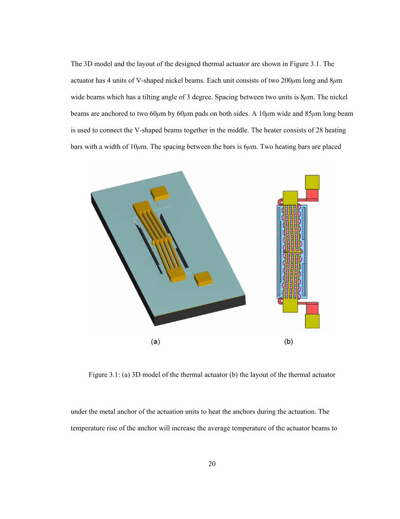
Figure 1.1: Anisotropic etching and isotropic etching..................................................................... 4 Figure 1.2: Fabrication steps to make a polysilicon cantilever by surface micromachining [6]..... 5 Figure 1.3: Example design of MetalMUMPs [7] ........................................................................... 6 Figure 1.4: MetalMUMPs layers (unit in micrometers, not to scale) .............................................. 7 Figure 2.1: Parallel plate electrostatic actuator.............................................................................. 10 Figure 2.2: Schematic of comb drive electrostatic actuator........................................................... 11 Figure 2.3: Photomicrograph of 200 μm long micromachined hot/cold arm thermal actuator [1] 14 Figure 2.4: Photomicrograph of 200 μm long micromachined chevron thermal actuator [1] ....... 14 Figure 2.5: An example of parallel capacitive sensor .................................................................... 16 Figure 2.6: Connecting the actuator to the sensor using a insulated bridge beam ......................... 17 Figure 3.1: (a) 3D model of the thermal actuator (b) the layout of the thermal actuator............... 20 Figure 3.2: Heater dimension (all units in micrometers) ............................................................... 21 Figure 3.3: 2D FEA model of the thermal transfer mode analysis ............................................... 23 Figure 3.4: Temperature profile of the thermal transfer analysis considering both convection and
conduction...................................................................................................................................... 26 Figure 3.5: Temperature profile of the thermal transfer analysis considering only conduction .... 27 Figure 3.6: Temperature profile along the vertical center line of the model ................................. 27 Figure 3.7: Velocity profile of the thermal transfer analysis considering both convection and
conduction...................................................................................................................................... 28 Figure 3.8: Complex features at the edge of the polysilicon structure........................................... 29 Figure 3.9: Boundary conditions used in the electro-thermal analysis .......................................... 30 Figure 3.10: 2D model used in electro-thermal analysis (a) Model 1; (b) Model 2; (c) Model 3.. 31 Figure 3.11: 3D FEA model of the electro-thermal analysis ......................................................... 33 Figure 3.12: Boundary conditions of the electrical analysis .......................................................... 34 Figure 3.13: Boundary conditions of the mechanical analysis ...................................................... 35 Figure 3.14: Temperature distribution of the indirect heating thermal actuator with a driving
voltage Vd of 20V.......................................................................................................................... 36 Figure 3.15: Temperature profile along the actuating beam.......................................................... 37
vii
Figure 3.16: Maximum temperatures of the heater and actuating beam as a function of the driving
voltage............................................................................................................................................ 37 Figure 3.17: Displacement of the thermal actuator as a function of the driving voltage ............... 38 Figure 3.18: Displacement of the thermal actuator with a driving voltage Vd of 24V as a function
of the force applied on the actuator tip .......................................................................................... 39 Figure 3.19: First four mode shapes of the thermal actuator ......................................................... 40 Figure 3.20: Picture of the fabricated MetalMUMPs thermal actuator ......................................... 41 Figure 3.21: Displacement as a function of the driving current: comparison between test and
simulation....................................................................................................................................... 42 Figure 3.22: Current as a function of the driving voltage: comparison between test result and
simulation results with different polysilicon and nickel layer thicknesses .................................... 43 Figure 3.23: Current as a function of the driving voltage: comparison between test result and
electrical-resistivity adjusted for different simulations.................................................................. 44 Figure 3.24: Displacement as a function of the driving current: comparison between test result
and electrical-resistivity adjusted for different simulations ........................................................... 45 Figure 4.1: Layout of the thermal actuator with integrated capacitive sensor ............................... 47 Figure 4.2: Movement mode of the capacitive plates (a) lateral mode; (b) transverse mode ........ 48 Figure 4.3: Dimensions of the capacitive sensor ........................................................................... 49 Figure 4.4: Capacitance of C1 and C2 as a function of the displacement of the movable plate set
....................................................................................................................................................... 52 Figure 4.5: Capacitance change of the sensor as a function of the displacement of the movable
plate set .......................................................................................................................................... 52 Figure 4.6: 2D electrostatic analysis model ................................................................................... 53 Figure 4.7: Electric field distribution of one unit of parallel plate................................................. 54 Figure 4.8: Tip of the parallel plate after fabrication ..................................................................... 54 Figure 4.9: Electric field distribution with rounded corners .......................................................... 55 Figure 4.10: Capacitance change as a function of displacement: comparison between analytical
result and FEA result ..................................................................................................................... 56 Figure 4.11: Picture of the fabricated thermal actuator with integrated capacitive sensor ............ 56 Figure 4.12: Experimental equipment setup .................................................................................. 57 Figure 4.13: Capacitance change as a function of the displacement: comparison of FEA and test
results ............................................................................................................................................. 58 Figure 4.14: Parasitic capacitances with the parallel plate capacitor............................................. 59
viii
Figure 4.15: The best fit curve for capacitance as a function of displacement .............................. 61 Figure 4.16: Flow chart of the manually tuning experiment.......................................................... 62 Figure 4.17: Driving voltage and capacitance change in the manual control experiment ............. 63 Figure 4.18: Comparison between the visually detected displacement result and the calculated
displacement from the capacitance change.................................................................................... 63 Figure 4.19: PI algorithm used in application................................................................................ 65 Figure 4.20: Hardware setup of the experiment............................................................................. 66 Figure 4.21: Test result of the capacitance change as a function of the displacement................... 67 Figure 4.22: Flow chart of the PI control program ........................................................................ 68 Figure 4.23: MS3110BDPC measured displacement result in the PI control experiment ............. 69
ix
List of Tables
Table 3.1: Material properties used in heat transfer mode analysis............................................... 25 Table 3.2: Simulation result of the three models ........................................................................... 32 Table 3.3: Material properties used in the 3D finite element analysis........................................... 35 Table 3.4: Natural frequency of the first four modes..................................................................... 40 Table 4.1: Sensor dimensions ........................................................................................................ 51
x
Symbols and Nomenclature
Symbol Parameter
A area
C capacitance
CMOS complementary metal-oxide-semiconductor
Cp specific heat capacity
DC direct current
E Young’s modulus
F force
FEA finite element analysis
FEM finite element method
FPGA Field Programmable Gate Array
g gravitational acceleration; gap between plates
IC integrated circuit
k thermal conductivity
Kp proportional gain
Ki integral gain
l length
MEMS Micro-Electrical-Mechanical-Systems
MUMPs Multi-User MEMS Processes
NEMS Nano-Electrical-Mechanical-Systems
P power
PCB print circuit board
PI Proportional Integral
PID Proportional Integral Derivative
p pressure
Q energy
R resistance
RMS root mean square
RF radio frequency
T temperature
t thickness; time
V voltage
w width
α thermal expansion coefficient
ε0 permittivity of free space
εr relevant permittivity
ρ resistivity; density
ξ temperature coefficient of the resistivity
η dynamic viscosity
dvκ dilatational viscosity
uv fluid velocity
xi
1
Chapter 1
Introduction
1.1 Introduction to MEMS
Micro-Electrical-Mechanical-Systems (MEMS) are integrated devices which are made up of
micro components such as actuators, sensors and electronic transistors. “Micro” indicates the
scale of the device; “electrical” indicates the involvement of electronics components;
“mechanical” indicates the usage of movable and flexible mechanical structures that could be
used for sensing and actuating; “systems” indicates the integration of different mechanical and
electrical elements to a system level device. In general, MEMS is a cross-disciplinary technology
that could develop micro scale integrated devices for various applications. The term MEMS is
widely used in North America. It is also called as Microsystems and/or Micromachines in other
countries.
The typical size of MEMS devices varies between tens to several hundreds micrometers and the
feature size may be as small as 1 micrometer. Because of the advantage of small scale, MEMS
devices have the following features:
• Fast response time. As the size of MEMS is reduced, the mass of the MEMS structure is
reduced as well. The resonance frequency of MEMS structures therefore increases. The
smaller the devices are made, the faster they can respond. A typical MEMS thermal actuator
has a response time of 60µs [1]. The response time of current commercial accelerometers is
smaller than 500µs. The fast response and high sensitivity make MEMS devices an excellent
2
candidate for sensing applications. For example, the MEMS accelerometers are widely used
as the sensing element for automobile safety airbags.
• Low power consumption. The compact MEMS devices require low power for actuating and
sensing. The hot/cold arm thermal actuator can be actuated with only several tens of mW [2].
Electrostatic actuators consume even less power. Besides the functional components power
consumption, the highly integrated nature of MEMS devices also reduces the power loss from
wiring. MEMS is also considered as a “green” technology as energy saving is becoming more
and more important.
• Low cost. Using fabrication technology which is widely used for complementary metal–
oxide–semiconductor (CMOS) fabrication in semiconductor industry, MEMS devices are
suitable for high volume production. The small scale of the devices reduces the cost of
material, packaging and shipping. For example, the commercial MEMS pressure sensor chip
for automobile application only costs a few dollars.
The traditional MEMS research is focused on micro sensors, micro actuators and
microcontrollers. MEMS accelerometers and pressure sensors have been deployed in automobiles
since the 1990s. Micro-machined inkjet printer nozzles have been used for high performance
inkjet printers since the 1970’s.
3
Nowadays, MEMS applications are classified more specifically. RF (radio frequency) MEMS
are defined as micro devices used for the telecommunication market, for example, RF switches,
tunable capacitors and resonators. Optical MEMS are applications which are focused on optic
networks and displays/scanners. Bio-MEMS are applications such as DNA filtering, cell
manipulation and biological sensing. With the size continuously reducing, Nano Electro
Mechanical Systems (NEMS) are starting to attract researchers to work on the nano scale
applications.
1.1.1 Micromachining techniques
The fabrication technology of MEMS originated from the microelectronics technology in the
semiconductor industry. The early development of MEMS technology can be traced back to the
1960’s when Dr. Richard Feynman gave his talk “There’s plenty of room on the bottom” on
December 29, 1959 at the annual meeting of the American Physical Society at the California
Institute of Technology. In 1978, K. E. Bean developed 3D structures on the silicon substrate
using anisotropic etching [3]. In 1982, K. E. Petersen published his famous paper “Silicon as a
Mechanical Material” [4]. This paper is widely referenced by MEMS researchers. In the same
year, R. T. Howe successfully fabricated micro cantilever beams with poly crystalline silicon
films using the fabrication technology which was used to make microelectronics integrated
circuits [5].
Based on current IC processing technology, two micromachining technologies are mainly used
for MEMS fabrication: surface micro-machining and bulk micro-machining. Both of these
methods employ the photolithography technique. Photolithography uses light to transfer patterns
4
from a photomask to a layer of photoresist. Photoresist is a light-sensitive material. Depending
on the type of photoresist, the exposed photoresist will be either hardened or weakened compared
to the unexposed part. Then the photoresist can be selectively removed with etching chemicals.
The remaining photoresist is used as a mask to pattern the material layer. In this step, the mask
protects the materials underneath from the etching and the unmasked materials are etched away to
form the desired planar micro structure shape.
1.1.2 Bulk micromachining
Bulk micromaching is a process to form 3D structures by etching into a bulk substrate. The
etching can be either isotropic or anisotropic. Isotropic etching is a non-directional material
removal method. The etchant removes the materials with the same etch rate in all directions.
Anisotropic etching takes advantage of the crystal structure of silicon. The atoms of single
crystalline silicon form a face-centered cubic structure. These periodic crystal structures make the
bond strength vary in different crystalline orientations. Some etchants have very different etch
rates on different crystalline orientations. By anisotropic etching, cavities with angled walls are
generated. A typical example of this is the appearance of <111> crystal plane sidewalls during
etching a <100> silicon wafer in Potassium hydroxide (KOH) etchant. Figure 1.1 shows examples
of isotropic etching and anisotropic etching. Bulk micromaching is commonly used to create deep
Figure 1.1: Anisotropic etching and isotropic etching
5
cavities for microfluidic channels and released hanging structures. Its general features are thicker
and larger compared to surface micromachining.
1.1.3 Surface micromachining
Surface micromachining builds up micro structures on the surface of a substrate. The process
normally uses two kinds of material layers to create 3D structures, a structural layer and a
sacrificial layer. The sacrificial layer and structural layer are deposited and patterned in
sequence. The sacrificial layer is used to separate structural layers. The connections between two
structural layers or between a structural layer and substrate will be made through the holes etched
in the sacrificial layer while the structural layer is patterned to form the structure features. At the
end of the process, the sacrificial layer is removed by wet etching to release the features from the
substrate to form a free standing structure. A simple process flow of how to create a cantilever
beam is shown in Figure 1.2. In this example, polysilicon is used as the structural layer and
silicon dioxide is used as the sacrificial layer.
Figure 1.2: Fabrication steps to make a polysilicon cantilever by surface micromachining [6]
6
Compared to bulk micromaching, surface micromaching create more complex microstructures by
depositing and patterning multiple structural layers in the vertical direction. For example, Sandia
Lab developed a five-layer process (SUMMiT V) which is able to create gear trains and hinges.
1.1.4 Metal MUMPs process
The devices in this thesis are fabricated with the MetalMUMPs process provided by MEMSCAP
Inc. The Multi-User MEMS Processes (MUMPs) use a standardized MEMS process which
merges several projects on the same wafer for volume manufacturing. Each project will use one
location of the wafer so that the cost will be shared. Because it provides researchers with cost-
effective access to prototyping with good reliability, it is widely used in MEMS research and
industry. The drawback of the MUMPs process is that the process must be standardized for all
users. It is not able to provide flexible customized steps for single researchers without significant
additional cost.
MetalMUMPs was introduced in 2003. Figure 1.3 shows the cross-section of a MetalMUMPs
design. MetalMUMPs process incorporates three major MEMS processes: thick metal
electroplating, bulk micromachining and surface micromachining. The process starts on an N-
Figure 1.3: Example design of MetalMUMPs [7]
7
type (100) silicon wafer. An isolating Oxide layer is grown from the substrate to provide electric
insulation. The trench is formed by KOH etching with the silicon nitride layer as mask. This
provides thermal and electrical isolation between the released structure and the substrate. Nitride1
and Nitride2 layers are silicon nitride layers which are used to encapsulate the polysilicon layer
and to connect nickel structures which can be electrically insulated. Poly is a polysilicon layer
that could be used as a resistor or for electrical crossover routing. Oxide2 is the sacrificial layer
which will be used to release the Metal structure. The metal combines 20μm nickel and 0.5μm
gold. Both materials are electroplated to form the mechanical structure and electrical connection.
GOLDOVP is a 1-3μm thick gold which is electroplated on the side of Metal to provide low
resistance electrical contact. Figure 1.4 illustrates all the layers used in this process. The details of
the MetalMUMPs process are available from MEMSCAP [7].
Figure 1.4: MetalMUMPs layers (unit in micrometers, not to scale)
8
1.2 Motivation
In the past twenty years, a wide variety of MEMS devices such as magnetic, electrostatic and
electro-thermal actuators have been investigated [8]. MEMS actuators are able to produce
mechanical motion on a small scale. Due to the advantages of such microscale phenomena as low
mass, strong electrostatic forces and rapid thermal response time, these devices feature compact
size, low power consumption and fast response. Among these actuators, thermal actuators
attracted a significant amount of research effort because they can generate large deflection and
force with a simpler design structure [9, 10]. Furthermore, their fabrication process is compatible
with general integrated circuit (IC) fabrication processes [11]. Thermal actuators are widely used
in areas such as actuating MEMS grippers, RF switches and micromirrors.
However, the accuracy of thermal actuators is heavily dependent on the working conditions, such
as temperature, humidity and pressure. It is hard to achieve accurate displacement control of the
thermal actuator without any position sensor. Moreover, there has been insufficient exploration of
thermal actuators that are integrated with position sensors to achieve feedback control. The
challenge of integrating sensors to actuators is the electrical insulation between the electrical
heating circuit and the sensing circuit. The traditional thermal actuators use resistive heating of
the actuation beams as the heat source. Therefore the actuators have electrical potential
distributed along the actuation beams. In order to integrate any sensors to these thermal actuators,
the sensor needs to be connected to the actuator via an electrical insulated material. This requires
additional fabrication process steps to add a dielectric bridge layer and can not be done
effectively by the current commercial MEMS fabrication processes.
9
1.3 Objective
The objective of this thesis has three parts:
• Design, simulate and characterize an indirect heating thermal actuator
• Integrate a capacitive sensor to the thermal actuator to sense the motion
• Achieve feedback position control of the thermal actuator
1.4 Thesis organization
The remainder of the thesis is organized as follows. Chapter 2 gives an overview on MEMS
actuators and sensors. Chapter 3 describes the concept, design, simulation and testing data of the
indirectly heated thermal actuator. Chapter 4 presents the integration of capacitive sensor to the
thermal actuator described in Chapter 3 and gives applications of manual tuning and feedback
control of the thermal actuator with the capacitive sensor read-out. The thesis is summarized and
future work is discussed in Chapter 5.
10
Chapter 2
Literature Review
This chapter will provide introduction to state of the art MEMS actuators and sensors. Special
attention will be given to thermal actuator and capacitive sensor, the main topic of the thesis.
2.1 Micro actuators
MEMS actuators are designed to provide small motions and generate small forces to actuate
MEMS devices. The applications include RF and optical switches, micro pumps, micro motors
and micro manipulators. One of the most commonly used MEMS actuators is the printer head
nozzle for inkjet printers. Depending on the actuating principle, MEMS actuators can be
classified as electrostatic actuators, thermal actuators, piezoelectric actuators and magnetic
actuators. Among those actuators, electrostatic and thermal actuators are the most commonly used.
2.1.1 Micro electrostatic actuator
Micro electrostatic actuators use the electrostatic force between two electrodes with different
electric potential to achieve the actuation. The simplest electrostatic actuator is the parallel plate
type as shown in Figure 2.1. Two electrical plates are parallel to each other with a dielectric gap
(usually air) between them. Usually one plate is anchored as a fixed electrode and the other is
connected to a spring structure as a movable electrode. When an electric potential is applied
Figure 2.1: Parallel plate electrostatic actuator
11
between the two plates, the electrostatic force will pull the movable plate closer to the fixed plate.
The electrical static force can be calculated by equation 2.1 [12].
2
20
2gLwVF rεε
= (Equation 2.1)
where ε0 is the permittivity of free space, εr is the reletive permittivity of the media between the
two plates, L is the length of the plate, w is the width of the plate and g is the gap between the two
plates. The main drawback of this simple actuator is the effect called pull-in. When the movable
plate moves toward the fixed plate by the electrostatic force, it deforms the mechanical spring.
Consequently the mechanical spring will provide a reaction force against the electrostatic force.
When the actuating voltage rises to a certain point, the resultant electrostatic force will be larger
than the retraction force that the spring cannot balance. Then the movable plate will be pulled
down to contact the fixed plate. This phenomenon is called pull-in effect. The pull-in effect limits
the actuation range of the parallel plate electrostatic actuator. This type of electrostatic actuator is
widely used for RF switches and micro pumps which do not require a large travel distance.
Figure 2.2: Schematic of comb drive electrostatic actuator
Comb-drive actuator is another type of electrostatic actuator which can overcome the pull-in
effect and achieve a larger displacement [13] [14]. Figure 2.2 shows a schematic of the comb-
12
drive actuator. When an electric potential is applied between the two sets of fingers, the
electrostatic force between the gap of two fingers in the x direction will be cancelled due to the
symmetry. The force in the y direction between each gap of the fingers can be calculated using
equation 2.2 [12].
gwVF r
2
20εε
= (Equation 2.2)
where w is the thickness of the finger. Since the finger thickness and gap are fixed, the force is
only proportional to the driving electric potential and independent of the moving distance in the y
direction. By this means, the comb-drive actuator can provide a large motion range. A larger
force can also be produced by increasing the number of actuation fingers.
Since the electrostatic actuator uses electrostatic force to actuate, the current only exists when
charging and discharging the electro plates. The power consumption is very low. But the
drawback of this type of actuator is that it needs a high voltage to generate the large displacement
and force. In order to reduce the actuating voltage, several methods to narrow the gap between the
electrodes have been proposed [14]. The drawback of narrowing the gap is that the reliability of
the actuator depends on the vibration. The vibration of the electro plates may cause a short circuit
which will result in failure.
2.1.2 Micro thermal actuator
Micro thermal actuators are actuators which generate motion by thermal expansion. When the
material temperature rises, the thermal expansion of the material will generate a small
displacement. The principal of thermal actuators is to amplify the asymmetrical thermal
13
expansion of a microstructure with variable cross sections or different materials. The heating
power comes from either the ohmic heating under a driving current through the structure or an
Figure 3.19: First four mode shapes of the thermal actuator
41
3.5 Experiments
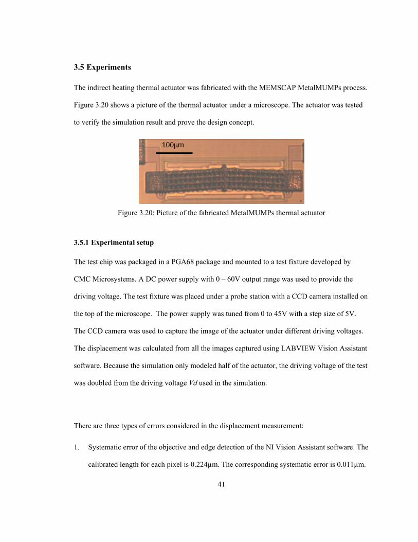
The indirect heating thermal actuator was fabricated with the MEMSCAP MetalMUMPs process.
Figure 3.20 shows a picture of the thermal actuator under a microscope. The actuator was tested
to verify the simulation result and prove the design concept.
100µm
Figure 3.20: Picture of the fabricated MetalMUMPs thermal actuator
3.5.1 Experimental setup
The test chip was packaged in a PGA68 package and mounted to a test fixture developed by
CMC Microsystems. A DC power supply with 0 – 60V output range was used to provide the
driving voltage. The test fixture was placed under a probe station with a CCD camera installed on
the top of the microscope. The power supply was tuned from 0 to 45V with a step size of 5V.
The CCD camera was used to capture the image of the actuator under different driving voltages.
The displacement was calculated from all the images captured using LABVIEW Vision Assistant
software. Because the simulation only modeled half of the actuator, the driving voltage of the test
was doubled from the driving voltage Vd used in the simulation.
There are three types of errors considered in the displacement measurement:
1. Systematic error of the objective and edge detection of the NI Vision Assistant software. The
calibrated length for each pixel is 0.224µm. The corresponding systematic error is 0.011µm.
42
2. Random error due to the vibration of the environment. The microscope vibrates with the
environment vibration sources during the measurement. This causes random error in the
measurement. Five samples are taken without a driving voltage applied to the actuator to
examine the vibration error. The RMS noise was found as 0.284µm.
3. Since the length/pixel ratio is calculated from the measured pixel width of the actuation
beam and the designed width, the random error exists because the beam width after
fabrication varies from the designed width. It has been documented that the fabricated beam
width of MetalMUMPs has a ± 10% variation from the designed width [40].
3.5.2 Test results and discussion
The simulation prediction and the test results of the displacement of the actuator as a function of
the driving current are shown in Figure 3.21. The simulation prediction and the test results show
Figure 3.21: Displacement as a function of the driving current: comparison between test and
simulation
43
the same trend. The simulation prediction is slightly lower than the test result. There are several
reasons which can affect the agreement of the simulation and test result:
1. The simulation employs a simplified model to avoid small surfaces which may cause
meshing problems and long calculation times. The modification of the model will
introduce errors into the simulation.
2. The MetalMUMPs process can not guarantee the fabricated chips have exactly the same
thickness as used in the simulation. The thickness of the nickel layer is μ m and
the thickness of polysilicon layer is
320 ±
70700 ± nm [10]. Figure 3.22 shows the simulation
result using the upper and lower limit of the thicknesses of the nickel layer and
polysilicon layer. The test result fits between the upper and lower limit simulation curves.
Figure 3.22: Current as a function of the driving voltage: comparison between test result and simulation results with different polysilicon and nickel layer thicknesses
44
3. From the MetalMUMPs process data sheet [10], the sheet resistance of the polysilicon
also varies from 19 to 25 ohm/sqare. Based on Equation 3-2, the resistivity of polysilicon
layer varies from to Ω.m. This process accuracy will also lead to a
mismatch between the simulation and test result. Figure 3.23 shows the current change as
a function of the driving voltage of the polysilicon heater. It is clear that the simulation
using Ω.m [10] and [17] does not fit the test result. The
measured resistance of the polysilicon heater under room temperature is 5.569 K Ω.
Assuming the dimension of the fabricated device is the same as the design dimension, the
values of resistivity and temperature coefficient of resistivity of polysilicon are tuned in
the FEM model to find the best fit value to the measurement data. As shown in Figure
3.22, values of Ω.m and were found here for proper
adjustment. Using the polysilicon properties obtained from Figure 3.23, the simulated
5102.1 −× 51093.1 −×
50 1074.1 −×=ρ 31025.1 −×=ξ
50 10833.1 −×=ρ 3105.1 −×=ξ
Figure 3.23: Current as a function of the driving voltage: comparison between test result and electrical-resistivity adjusted for different simulations
45
displacement curve was compared to the measured displacement in Figure 3.24 and
shows a better agreement.
Figure 3.24: Displacement as a function of the driving current: comparison between test result and electrical-resistivity adjusted for different simulations
4. In the FEA model, the heater is considered as having no displacement at any time. The
gap between the heater and the actuating beams is a constant value of 1.1 μ m. But in the
experiment, the heater deforms upward due to the thermal expansion. This deformation
decreases the gap value and therefore makes a difference to the FEA model. But, due to
the calculating capability limitation of the software, the deformation of the heater is not
included into the simulation. This will also effect the agreement between the simulation
and experiment.
46
The above factors all contribute to the difference between the experiment and simulation. As
shown in Figure 3.24, the simulation can be improved by adjusting the polysilicon electrical
resistivity properties. The simulation method in this thesis can give a reasonable estimate of the
behavior of the thermal actuator.
3.6 Summary
As discussed above in this chapter, the model method for finite element analysis of the indirect
heating thermal actuator is reported. The dominant heat transfer mode was found to be conductive
heat transfer. A model simplification method is also discussed and used in the analysis. The
device was fabricated and tested to verify the simulation prediction. The result shows that the
simulation has a reasonable agreement with the experimental data.
47
Chapter 4
Thermal Actuator with Integrated Capacitive Sensor
4.1 Introduction
As discussed in Chapter 3, traditional thermal actuators directly apply a driving voltage to the
actuation beams. The driving electrical potential is distributed on the actuation beams. This will
interfere with the electrical signal of the integrated position sensor unless a dielectrical material is
used as a connector between the actuator and the sensor. Unlike traditional thermal actuators, the
indirect heating thermal actuator uses an insulated heater to drive the actuation beams. The
electrical potential on the heater will not interfere with the electrical potential of the actuation
beams. Taking advantage of this feature, a capacitive sensor can be connected to the actuator
beams for sensing the motion of the actuator.
Figure 4.1: Layout of the thermal actuator with integrated capacitive sensor
In order to achieve a compact size while retaining high sensitivity, the micro parallel plate
capacitive sensor configuration is selected. The layout is shown in Figure 4.1. The movable plate
48
set is located in the middle while the two stationary plate sets are on the two sides of the movable
plate set. The configuration provides several sets of parallel capacitors. Those capacitors are
connected in parallel on each side to form two capacitors C1 and C2 as shown in Figure 4.1.
The capacitive sensor can be classified into two modes: lateral mode and transverse mode. In the
lateral mode, as shown in Figure 4.2 (a), the capacitive plate moves along the x direction. It
Figure 4.2: Movement mode of the capacitive plates (a) lateral mode; (b) transverse mode
changes the overlapping area of the parallel plate capacitor. According to Equation 2.2,
capacitance change is linearly related to the overlapping area change of the parallel plate
capacitor. The sensitivity of the sensor can be calculated by:
gt
xC rεε 0=∂∂ (Equation 4.1)
where t is the width of the parallel plate. From Equation 4.1, the sensitivity does not change when
the movable plate moves. Moreover, the motion range of the plate is only limited by the gap
between the tip of the movable plate to the root of the fixed plate. Increasing the gap between the
tip of the movable plate to the root of the fixed plate does not affect the sensitivity of the sensor.
By these means, the lateral sensing mode is suitable for applications which require sensing a large
motion range. In the transverse mode, as shown in Figure 4.2 (b), the capacitive plate moves
49
along the y direction which changes the gap between the two sensing plates. The sensitivity of the
sensor can be calculated by:
20
)( yglt
yC r
−=
∂∂ εε (Equation 4.2)
where y is the displacement of the movable plate. Comparing Equation 4.1 and Equation 4.2, if
the length of the plate l is larger than the gap between the two plates g, the sensitivity of the
sensor in transverse mode is higher than in the lateral mode. Moreover, when the movable plate
moves closer to the fixed plate, the sensitivity will increase. The drawback of the transverse mode
is the non-linearity between the capacitance change and the gap change as indicated by Equation
4.2. The detection range is limited by the gap between the two sensing plates. When the motion is
greater than the gap between the two sensing plates, the two sensing plates will contact each other.
The transverse mode is suitable for applications which require sensing a small motion range.
Figure 4.3: Dimensions of the capacitive sensor
Considering the thermal actuator described in Chapter 3 has a small motion range, the transverse
mode is selected to achieve a better sensitivity. With the configuration shown in Figure 4.3, the
50
capacitance change of C1 and C2 are opposite to one another. The advantage of this configuration
will be discussed in the analytical analysis part of this chapter.
4.2 Analytical analysis
The variable capacitors C1 and C2 have similar dimensions as shown in Figure 4.3. Each of them
has four variable capacitor units. Each capacitor plate is spaced at g1 and g2 to the adjacent plate.
For the variable capacitor C1, the capacitance of each variable capacitor unit can be presented by
three types of capacitors C11, C12 and Cp. C11 represents the capacitance between the two plates
with a gap of g1. C12 represents the capacitance between the two plates with a gap of g2. Cp is the
capacitance between the plate tip and the root of the other plate. The capacitances can be
calculated by
ggltC r
Δ−=
1
011
εε (Equation 4.3)
ggltC r
Δ+=
2
012
εε (Equation 4.4)
3
0
gdtC r
pεε
= (Equation 4.5)
where is the displacement of the movable plate set, d is the width and t is the thickness of
the plate. The total capacitance of C
gΔ
1 is:
prp Cgggg
ltCCCC 6)34(63421
012111 +Δ+
+Δ−
=++= εε (Equation 4.6)
The total capacitance of C2 can be calculated in the same way:
51
pr Cgggg
ltC 7)34(21
02 +Δ−
+Δ+
= εε (Equation 4.7)
The capacitive sensor will output the differential reading of C1 and C2. The output capacitance
can be calculated by:
prS Cgggg
gltCCC −Δ−
+Δ−
Δ=−= )68(22
222
1021 εε (Equation 4.8)
From Equation 4.8, the only fixed capacitance term left is Cp. Most of the fixed capacitances are
eliminated with the differential capacitance reading configuration. In order to further eliminate
the parasitic effect, the capacitance change from the original position is used:
)68()0()(22
222
10 gggg
gltCgCC rsss Δ−+
Δ−Δ=−Δ=Δ εε (Equation 4.9)
In this way, all the fixed capacitances are eliminated. sCΔ is used to determine the position of
the actuator.
Table 4.1: Sensor dimensions
Symbol Length (µm)
t 20
l 200
g1 8
g2 24
g3 8
W 8
The dimensions of the capacitance sensor are shown in Table 4-1. The capacitances as a function
52
of the displacement of the two capacitors C1 and C2 are shown in Figure 4.4. The capacitance
change of the sensor is shown in Figure 4.5. From the figures it is clear that the sensitivity of C1
and the differential capacitance increase significantly when the gap between the two sensing
plates increases.
Figure 4.4: Capacitance of C1 and C2 as a function of the displacement of the movable plate set
Figure 4.5: Capacitance change of the sensor as a function of the displacement of the movable plate set
53
4.3 Finite element analysis
The finite element analysis (FEA) of the capacitive sensor was simulated using COMSOL
Multiphysics with the electrostatics solver. Because the sensor has a planar structure, 2D analysis
was used to simplify the calculations. The 2D analysis model is shown in Figure 4.6. The sensor
is modeled inside a 1200µm by 600µm air block. The outer boundary of the air block is treated as
an infinite plane. The middle parallel plate set is grounded while the two fixed parallel plate sets
are connected to the nominal voltage Vs and –Vs separately to calculate the capacitance.
Figure 4.6: 2D electrostatic analysis model
54
Figure 4.7: Electric field distribution of one unit of parallel plate
Figure 4.7 shows the electric field distribution of one unit of parallel plate when Vs is equal to one
volt. The color plot presents the nominal electric field value while arrows present the electric field
direction. The electric field at the tips of the plates has a greater value than at other locations. This
is because the tip has a 90 degree corner. Energy concentrates on the very sharp tip point which
results in a large electric field value. Due to the fabrication resolution limit, the tip of the plate has
a rounded shape instead as shown in Figure 4.8. The true energy concentration effect will be
Figure 4.8: Tip of the parallel plate after fabrication
55
much smaller than predicted in the simulation. The electric field at the tip in the real device will
be smaller than the simulation result. One unit of parallel plate with rounded corners of 4µm
radius was also simulated. As shown in Figure 4.9, the maximum electric field value is only 48%
of the maximum electric field value of the original model. The result agrees well with the
assumption. The capacitance of the unit with rounded corners is 6.35fF while the capacitance of
the original model is 6.27fF. The difference of the capacitance is only 1.2%. This shows that the
rounded corner has little effect on the capacitance of the sensor. It is safe to use the model with 90
degree corners to calculate the capacitance. The capacitance change as a function of the
Figure 4.9: Electric field distribution with rounded corners
56
displacement for both analytical and FEA investigations are shown in Figure 4.10. This figure
shows a good agreement between the two results.
Figure 4.10: Capacitance change as a function of displacement: comparison between analytical
result and FEA result
4.4 Test result
4.4.1 Experiment setup
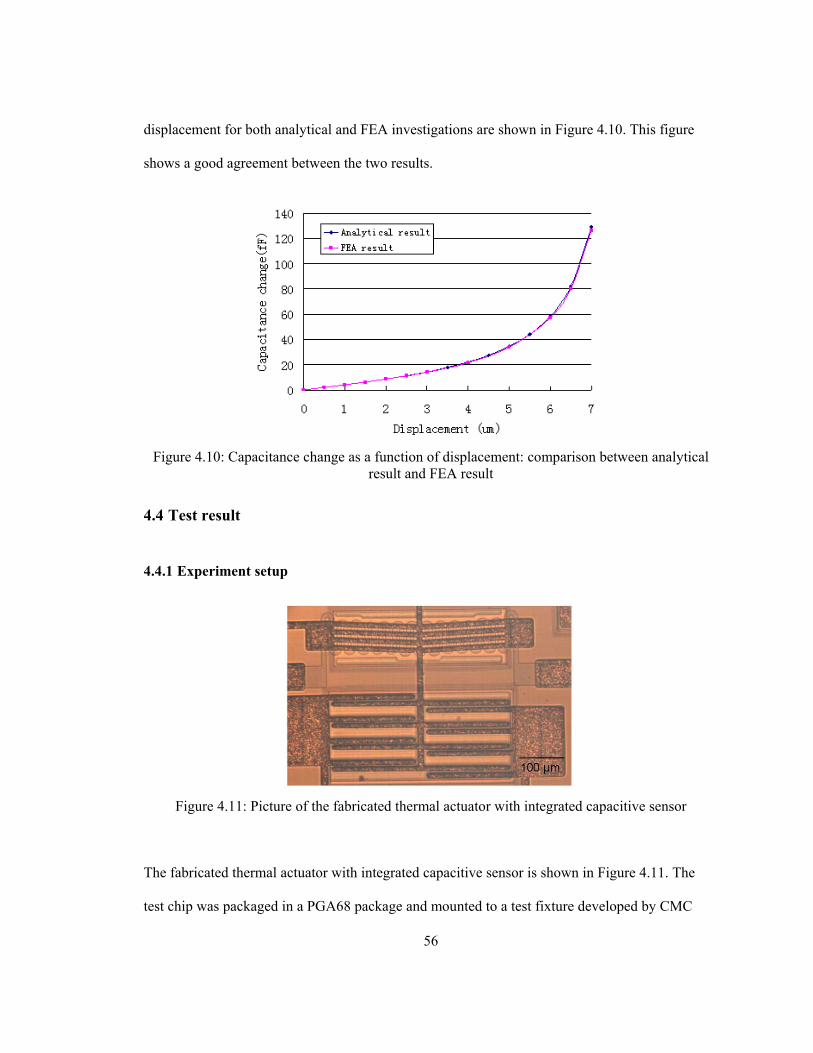
Figure 4.11: Picture of the fabricated thermal actuator with integrated capacitive sensor
The fabricated thermal actuator with integrated capacitive sensor is shown in Figure 4.11. The
test chip was packaged in a PGA68 package and mounted to a test fixture developed by CMC
57
Microsystems. The thermal actuator setup is the same as the test setup described in Chapter 3.
The capacitance was measured using an AD7746 evaluation board made by Analog Devices. The
capacitance to digital output conversion was done using an AD7746 IC. The two sensing variable
capacitors were connected directly to the device inputs on the board. Figure 4.12 shows the whole
experimental setup. In each measurement, first the driving voltage was applied to the thermal
actuator, and then the displacement and the differential capacitance output were recorded. In
order to reduce the effect of the noise in the capacitance conversion, 100 samples were taken in
each measurement with a sample rate of 10.96.1Hz and the average result was considered as the
measurement data.
Figure 4.12: Experimental equipment setup
4.4.2 Test results and discussion
The FEA and the test results of the capacitance change of the capacitive sensor as a
58
Figure 4.13: Capacitance change as a function of the displacement: comparison of FEA and test
results
function of the displacement are shown in Figure 4.13. The Y axis error bar at each measured
point is the root mean square (RMS) noise of that capacitance measurement. From the figure, the
test result shows a reasonable agreement with the simulation results. There are several reasons
which can affect the agreement of the simulation and test results.
1. The factory calibrated accuracy of the AD7746 chip is ±4 fF and the resolution is down to
4aF; however, the wiring between the capacitance reading board and the sensor introduces
noise which affects the precision of the capacitance measurement. In the experiment, three
jump wires were used to connect the test fixture to the AD7746 evaluation board. Any
motion of the wires during the measurement has significant effect on the reading. In the
experiment, any physical disturbance of the experimental setup was avoided. However, the
59
vibration of the wires due to the ambient environment could not be completely eliminated.
One hundred samples were measured under the experimental setup with 0 volts driving
voltage. The average capacitance reading was -0.359 fF. The RMS noise was 0.529 fF while
the peak-to-peak noise was 3.025 fF. According to simulation data, the capacitance change
for a 3µm displacement was 14.22 fF. The noise level was high compared to the capacitance
change range of the sensor. Using the average value of 100 samples in each measurement
can help to improve the accuracy but only results in a limited improvement. In order to
further reduce the noise, the capacitance readout circuit needs to be improved. For example,
the test chip and the AD7746 readout circuit should be arranged to fit in one PCB board to
avoid any floating wires.
2. In the analytical model, Equation 4.6 and Equation 4.7 only considered the parasitic
capacitance of the sensor. In real conditions, parasitic capacitance also exists in the wires
which connect the sensor to the capacitance readout circuit. It can be in series with the
sensing capacitor, such as from poor ohmic contact between the pins of the PGA68 package
and the sockets. It can also be in parallel with the sensing capacitor, such as the capacitance
between the wires connected to the fixed parallel plate sets and the movable parallel plate set.
Figure 4.14 shows a lumped circuit model which considers the parallel plate capacitor set C1
Figure 4.14: Parasitic capacitances with the parallel plate capacitor
60
with two parasitic capacitors: Cp1 is in series with the parallel plate capacitor while Cp2 is
connected in parallel. The measured capacitance Cm is given by
211
11p
p
pm C
CCCC
C ++
= (Equation 4.10)
From Equation 4.9, Cp2 can be eliminated in the calculation of the capacitance change.
Unfortunately, Cp1 contributes to the difference between the test result and the simulation
result.
3. As mentioned in Chapter 3, the MetalMUMPs process can not guarantee the fabricated chips
have exactly the same thickness as used in the simulation. The thickness of the nickel layer is
20±3µm. The variation range is ±15%. From Equation 4.9, this variation will also result in a
15% variation of the measured capacitance change.
The factors mentioned above are the possible reasons for the misalignment of the simulation
result and the test result.
4.5 Feedback control applications of the thermal actuator with integrated capacitive
sensor
4.5.1 Manual tuning of the displacement according to the sensor readout
The displacement of the thermal actuator can be affected by many factors such as humidity,
pressure, and air flow rate [41]. These factors can change the heat loss rate from the actuator to
the ambient air. Beside these, the actuator under external load has a different displacement
compared to the no load condition. Predicting the displacement with the driving voltage is not
61
accurate, especially when an external force is applied. The capacitance change of the capacitive
sensor is directly related to the displacement of the movable plates. With the integrated capacitive
sensor, the displacement of the thermal actuator can be detected more accurately. In this
application, the displacement of the actuator was tuned manually according to the capacitance
change read-out.
Figure 4.15: The best fit curve for capacitance as a function of displacement
As shown in Figure 4.15, the function between displacement d and capacitance change ΔC can be
derived from the best fit curve using a second-order polynomial as:
ddC 3524.28531.0 2 +=Δ (Equation 4.11)
Equation 4.11 is used to determine the displacement of the actuator during the manual tuning
experiment. The flowchart that describes the manual tuning is shown in Figure 4.16. The driving
voltage is tuned manually to adjust the displacement. If the capacitance reading is lower than the
62
desired value, the driving voltage will be increased and vise versa. The tuning will be finished
when the difference between the capacitance change read-out value and the desired capacitance
change value is smaller than the error tolerance Ce , which is the RMS noise (0.529fF) taken from
the experiment in section 4.4.2.
Otherwise
>Ce <-Ce
Increase driving voltage
Read capacitance
Cm- C0- Cd
Achieve desired position
Desired displacement
Calculate the desired capacitance change Cd
Read initial capacitance C0
Increase driving voltage Decrease driving voltage
Figure 4.16: Flow chart of the manually tuning experiment
In the experiment, the desired displacement was set to be 2 µm. The capacitance change value
was 8.12 fF according to Equation 4.11. In order to minimize the error of the capacitance reading,
100 samples were taken at each measurement to get an average result. It took 8 tuning steps to
achieve the desired displacement. Figure 4.17 shows the driving voltage and capacitance change
results of the experiment. The final driving voltage was 31V and the capacitance change was
8.35fF. The estimated displacement according to the capacitance change was 2.04 µm.
63
Figure 4.17: Driving voltage and capacitance change in the manual control experiment
Figure 4.18: Comparison between the visually detected displacement result and the calculated
displacement from the capacitance change
In order to verify the performance of the manual tuning, the displacement of each step was
captured with a camera. Figure 4.18 shows the comparison of the visual detection result and the
calculated displacement from the capacitance change result at each tuning step. The two curves
show a reasonable agreement. The disagreement between the displacement from the visually
detected result and the capacitance result results from:
64
1. The high noise level of the capacitance readout circuit;
2. Equation 4.11 was derived from the best fit second-order polynomial curve. It can only give
a reasonable estimate between the capacitance change and displacement.
4.5.2 Closed-loop Feedback control of the displacement according to the sensor readout
Besides the manual tuning of the displacement of the thermal actuator, the developed thermal
actuator with integrated capacitive sensor can also be controlled automatically with a closed-loop
feedback control method. The closed-loop feedback control was investigated as a means to
improve the dynamic behavior of the actuator with fast response time, precise position control
and continuous tuning of position. In this section, a Proportional Integral (PI) feedback control
method is studied.
The PI feedback control method used in this application is based on a generic closed-loop
feedback Proportional Integral Derivative (PID) algorithm. Three reaction parts are weighted and
summed to output the final reaction: Proportional, Integral and Derivative. The proportional part
reacts based on the current error between the desired position and current position while the
integral part reacts based on the sum of past errors and the derivative reacts based on the
changing rate of the current error. The derivative reaction helps to reduce the overshoot. The
drawback is that the noise in the error signal is amplified during the numerical differentiation of
the error signal for obtaining the derivative of the error [42]. Since the derivative reaction leads to
a high sensitivity to noise, this application only used a PI algorithm as illustrated in Figure 4.19.
65
τderrorIτ
ik ∫0 )(τ
)(terrorP k p×
Σ Error Σ Position Output
–
+Desired
Position
Feedback loop
Figure 4.19: PI algorithm used in application
The PI controller was implemented into a MEMS/FPGA Platform provided by CMC
Microsystems. The MEMS/FPGA Platform includes an AMIRIX AP1000 FPGA Board, and a
PMC66-16AISS8AO4 Analog Input/Output Module. The AP1000 FPGA board is used to
calculate the reactions based on the PI algorithm. This step was done by implementing the PI
algorithm codes into a standard MEMS/FPGA input/output reference code package. The Analog
Input/Output Module was used to convert the analog capacitive sensor input signal to a digital
signal for the FPGA board and the digital output signal from the FPGA board to an analog signal
to control the thermal actuator. Since the Analog Input/Output Module can only provide a ±10V
and up to 3mA driving signal, a Tabor 9400 Power Amplifier with 50x amplification was used to
amplify the signal to the driving voltage needed for the thermal actuator. Because the AD7746
can only generate a digital output signal through an I2C data bus, which is not compatible with the
analog input requirement of the MEMS/FPGA platform, a capacitance reading board
MS3110BDPC with a Universal Capacitive Readout IC MS3110 (by IRVINE SENSORS
Corporation) was used instead. The MS3110 capacitive readout IC converts the capacitance
change into an analog voltage signal with an accuracy of ±4 fF. The hardware setup is shown in
66
Figure 4.20. The relationship between the output voltage of the MS3110BDPC board and the
capacitance can be described as:
)25.2(20 −= VoutC (fF) (Equation 4.12)
AP1000 FPGA (PI Controller)
and AIO Module
Tabor 9400 Power Amplifier
MS3110BDPC Board
Thermal Actuator with Sensor
Host PC
Tabor 9400
MS3110BDPC
MEMS Chip and fixture
Figure 4.20: Hardware setup of the experiment
The same experimental setup as the one used with the AD7746 evaluation board was used to test
the capacitance change according to the displacement using the MS3110BDPC board. Similar to
the experiment with the AD7746 evaluation board, the capacitance readout accuracy with the
MS3110BDPC board also suffered from noise. Besides the noise that exists in the wiring between
the capacitive sensor and the capacitance reading IC, the analog to digital conversion of the
Analog Input/Output Module also generated noise to the whole system. In order to minimize the
noise, 256k (256 x 1024) samples were taken at each reading and the average result was
considered as the measurement data. The first measurement was done with 0 Volts driving
voltage. The result shows that the capacitance output from the MS3110BDPC board was 7.7 fF
with a RMS noise of ±0.562 fF. The capacitance change measurement results at different
67
displacements are shown in Figure 4.21 in comparison with the FEA result. From this figure, the
test result shows a reasonable agreement with the FEA result. The function between displacement
d and capacitance change ΔC is illustrated in a second-order polynomial from the best fit curve of
the test results:
ddC 0107.42519.0 2 +=Δ (Equation 4.13)
Equation 4.13 is used as the transfer function between displacement and capacitance change in
the PI control algorithm.
Figure 4.21: Test result of the capacitance change as a function of the displacement
68
The flow chart of the PI control program is shown in Figure 4.22. The program will read the
desired displacement input from the user at the beginning and convert it to the corresponding
desired voltage output change of the MS3110 BDPC board. Before applying the driving voltage,
the initial capacitance value of the sensor is measured and used to calculate the capacitance
change. Then the feedback control loop will start. In each cycle, the current capacitance value is
Receive stop signal?
No
Yes
Stop feedback control loop
Set desired displacement
Calculate the desired MS3110BDPC output voltage change Vdes
Read initial MS3110BDPC output voltage V0
Start feedback control loop
Read current MS3110BDPC output voltage Vi
Calculate error V i-V0 -Vdes
Calculate driving voltage using PI algorithm and sum the past
errors
Output the driving voltage signal
Figure 4.22: Flow chart of the PI control program
69
measured and applied to the PI algorithm. The calculated driving voltage is then output to the
thermal actuator through the high voltage amplifier. In order to protect the thermal actuator, the
driving signal is constrained between 0-0.8 V so that the driving voltage to the thermal actuator is
between 0-40 V. Since 256k samples are taken in each measurement, the cycle time of each loop
is around 5 seconds.
In the experiment, the best fit value of Kp and Ki was found to be 6.8 and 0.005 respectively.
Figure 4.23 shows the test result with the PI feedback control of the thermal actuator to achieve a
displacement of 2 µm. In the figure, the displacement is calculated by the measurement of the
capacitance change. The result shows that the displacement can be controlled by the PI controller
to stay close to the desired value. But the displacement result varies in a ±0.25 µm range. This
variation can be explained as follows:
Figure 4.23: MS3110BDPC measured displacement result in the PI control experiment
70
1. The high noise level of the capacitance readout circuit is the main reason for the variation.
The RMS noise of ±0.562 fF can be translated to ±0.135 µm displacement error. This error
affects the PI control in two ways. On one hand, it made the measured displacement value
offset from the real displacement of the actuator. On the other hand, the error is added in the
PI control calculation and causes a false driving voltage reaction. In this experiment, 256K
samples are taken in each measurement to minimize the effect of the noise.
2. The output analog voltage signal from the PMC66-16AISS8AO4 Analog Input/Output
Module contains noise. With a 0V DC signal generated by the analog input/output module,
the peak-to-peak noise was measured by the oscilloscope to be 100mV. This noise was
amplified by the Tabor 9400 power amplifier to 5V. Compared to the driving voltage range
0-40V in this application, the noise causes an unpredictable displacement variation.
Besides the significant error issue, this PI control application also suffered from the 5 second
cycle time of each control loop. Compared to the fast response time of the MEMS thermal
actuators, the slow cycle time is not suitable for the application. The slow cycle time is caused by
sampling of 256k samples at each measurement. If the noise ratio can be reduced, the cycle time
can be reduced to around 0.5 seconds by reducing the sampling number to 1k.
4.6 Summary
In this chapter, a novel thermal actuator with integrated capacitive position sensor was introduced.
The analytical model, FEA and test results for the capacitive sensor were presented to validate the
design concept. The test results showed a reasonable agreement with the analytical analysis and
71
the FEA. A manually displacement tuning application and a PI feedback control application were
done with the designed thermal actuator with integrated capacitive sensor. Although the current
design contains a high noise ratio, it shows a good potential to be used in feedback control
applications.
72
Chapter 5
Conclusion
In the first part of this thesis, the finite element analysis of an indirect heating thermal actuator
was documented. The heat transfer analysis revealed that the heat loss through convective heat
transfer can be neglected. The dominant heat transfer mode was found to be conductive heat
transfer. A simplified model was used in the electro-thermal analysis and the difference to the
result from the original model was less than 1.5 percent. Using this simplified model, the number
of small faces in the model is reduced significantly. In this way, the meshing failure related to
those small faces was avoided and the number of elements reduced. From the thermal-mechanical
analysis, the maximum displacement of the thermal actuator with no load was found to be ~3 µm.
With a constant driving voltage, the relation between the displacement change of the actuator and
the load applied to the actuator tip can be approximated using a linear function with a spring
constant of 2.69 kN/m. The test result of the thermal actuator was higher than the simulation
result. This difference is due to the process tolerance of the layer thickness and the resistivity and
temperature coefficient of the resistivity. The resistivity and temperature coefficient of the
resistivity was calibrated with the experiment data. The FEA with the adjusted material properties
showed a good agreement with the test result.
In the second part of the thesis, a novel thermal actuator with integrated capacitive sensor is
presented. Using the indirect heating method, the electrical heating circuit is well insulated from
the capacitive sensing circuit to achieve the integration of the thermal actuator and capacitive
sensor. This novel design has the ability to measure the displacement of the thermal actuator
using the capacitive sensor. With this feature, thermal actuator feedback control applications are
73
enabled. In the analytical model, equations are derived to calculate the capacitance of the
capacitive senor. FEA results verified the analytical model. Good agreement was found between
the FEA results and the analytical model results. The design was fabricated with MetalMUMPs
13 run at MEMSCAP. The test results showed a reasonable agreement with the simulation results.
Two feedback control applications were tested with the thermal actuator with capacitive sensor.
One application incorporated manual tuning of the displacement according to the sensor readout.
The other application involved closed-loop feedback control of the actuator using a PI controller
implemented using the MEMS/FPGA platform provided by CMC Microsystems. Although the
test results from the two applications suffered from significant noise, they showed the potential of
using the design for feedback control applications.
74
Chapter 6
Recommendation Future Work
The main problem of the thermal actuator with integrated capacitive sensor is the high noise of
the capacitance sensor. Several future investigations are recommended to solve this problem,
1. The number of sensor plates should be increased in future designs to increase the sensitivity
of the sensor. In this way, the capacitance change output for the same displacement will be
increased. Since most of the noise exists in the wiring circuit between the sensor and the
capacitance reading IC, the noise of the system will not change. The signal-to-noise ratio
will be increased.
2. A customized PCB board should be designed to assemble the MEMS chip and the
capacitance reading IC. Compared to the setup described in this work, the customized PCB
board should reduce the noise in several ways:
a) The floating wires will be removed from the circuit. The vibration and movement of the
floating wires are the main source of the noise in the measurement. This will be
removed.
b) The redundant components on the capacitance readout IC evaluation board will also be
removed. Those components and related wiring will no longer interfere with the readout
circuit.
c) By carefully arranging the wiring route of the PCB board, the connection between the
sensor and the capacitance readout IC could be shortened and arranged symmetrically.
75
This will reduce the parasitic capacitance and also reduce the interference with the
surrounding environment.
3. Since the analog input/output module of the MEMS/FPGA platform generates noise when
converting between the analog and digital signal, the PI controller should be implemented in
LABVIEW to control the system. LABVIEW can import data using an I2C data bus through
the NI USB-8451 I2C/SPI Interface device. The AD7746 capacitance reading IC can be used
instead of the MS3110 to avoid the noise in the analog to digital signal conversion. A high
precision DC power supply controlled by LABVIEW should be used as the driving voltage
output device. This output driving signal setup will have much less noise than the analog
input/out module/Tabor 9400 power amplifier setup.
After all this work is done, the noise should be reduced significantly. The number of samples
needed for each control loop will also be reduced so that the efficiency of the PI controller will be
improved.
76
References
[1] R. Hickey, D. Sameoto, T. Hubbard, M. Kujath, “Time and frequency response of two-
spoke micromachined thermal actuators”, J. Micromech. Microeng. 13 (2003) 40–46.
[2] Q.-A. Huang, N.K.-S. Lee, “Analysis and design of polysilicon thermal flexure actuator”, J.
Micromech. Microeng. 9 (1999) 64–70.
[3] K.E. Bean, “Anisotropic etching of silicon”, IEEE Transaction on Electron Devices, 1978,
ED25: 1185-1193
[4] K. E. Petersen, “Silicon as a Mechanical Material”, Proc. Of the IEEE, 79 (1982), 420-457
[5] R. T. Howe and R. S. Muller, “Polycrystalline silicon micromechanical beams”, in spring
meeting of the electrochemical society, Montreal, Canada, Extended abstracts 82-1. May 9-
14, 1982.
[6] P. Yang, “How to create a MEMS Pro Design kit for a MEMS or microfluidic process”,
double disp, disptemp; // end of PID variables if (argc < 2) printf("missing argument\nusage: testapp [0|1|2|...]\n"); return (1); strcat(driverName, argv[1]); // open the driver. fd = open(driverName, O_RDWR); if (fd < 0) printf("%s: can not open device %s\n", driverName); return (1); fd1 = open("/dev/hwlogic", O_RDWR); if (fd1 == -1) printf("Cannot open /dev/logic\n");
87
return (1); // set timeout for reading and writing. param = 5; //seconds res = ioctl(fd, IOCTL_DEVICE_SET_TIMEOUT, ¶m); if (res < 0) printf("ioctl IOCTL_DEVICE_SET_TIMEOUT failed\n"); goto OUT; res = ioctl(fd, IOCTL_DEVICE_INITIALIZE, NULL); if (res < 0) printf("ioctl IOCTL_DEVICE_INIT failed\n"); goto OUT; printf("board init OK\n"); // input desired capacitor value printf("\n/********************************************/\n"); printf("Please enter desired displacement:\n"); scanf("%lf", &value); printf("The desired displacement entered is: %f \n", value); //setup for input channel 0 if(setupRead()) printf("the setupRead() failed!\n"); V01d = 0.0; // start value of V01d V01 = 0.0; ij =0; input_C_value =0.2519*(double)value*(double)value+4.0107*(double)value; printf("The desired capacitance change is: %f \n", input_C_value); while(ij < 1000) if(setupWrite0()) printf("the setupWrite0() failed!\n"); //Generate sine wave and send out by output channel 0 /* initialize the outputBuffer */ dataValue=0;
88
for (i=0;i<WORDS_TO_SEND;i++) //Created incrementing data and incrementing channel tag. outputBuffer[i]=dataValue&0xFFFF; /* Generate data and save them in the outputBuffer */ for (i=0;i<WORDS_TO_SEND;i++) x = (double) timeStep /1.0; timeStep++; sample = V01d; outputBuffer[i] = (unsigned int)sample; outputBuffer[WORDS_TO_SEND-1] = outputBuffer[WORDS_TO_SEND-1] + 0X10000; /* write data into the output channel buffer */ bytesWritten = write(fd, outputBuffer, WORDS_TO_SEND); if (bytesWritten <= 0) printf("\nread error -> after write..res \n"); goto OUT; param = TRUE; res = ioctl(fd, IOCTL_DEVICE_ENABLE_OUT_CIRC_BUFFER, ¶m); if (res < 0) printf("ioctl IOCTL_DEVICE_ENABLE_OUT_CIRC_BUFFER failed\n"); goto OUT; param = TRUE; res = ioctl(fd, IOCTL_DEVICE_ENABLE_OUT_CLK, ¶m); if (res < 0) printf("ioctl IOCTL_DEVICE_ENABLE_OUT_CLK failed\n"); goto OUT; //read the input buffer reg and save the data to the inputBuffer for(i=0; i<IN_BUFFER_SIZE; i++) //printf("at the begining of the first for loop\n"); rw_q.ulRegister = BOARD_CTRL_REG; rw_q.ulValue = 0L; res = ioctl(fd, IOCTL_DEVICE_READ_REGISTER, &rw_q);
89
param = rw_q.ulValue; if(param & 0x00008000L)//Check overflow bit printf(" Input buffer overflow\n"); rw_q.ulValue = param | 0x00000800L; //Set SW trigger. res = ioctl(fd, IOCTL_DEVICE_WRITE_REGISTER, &rw_q); rw_q.ulValue = 0L; res = ioctl(fd, IOCTL_DEVICE_READ_REGISTER, &rw_q); param = rw_q.ulValue; while(param & 0x00000400L) ; rw_q.ulRegister = ANALOG_INPUT_REG; rw_q.ulValue = 0L; res = ioctl(fd, IOCTL_DEVICE_READ_REGISTER, &rw_q); inputBuffer[i] = rw_q.ulValue & 0x0000ffffL; inputBuffer[IN_BUFFER_SIZE-1] = inputBuffer[IN_BUFFER_SIZE-1] + 0X10000; for(i=0; i<1024; i++) sum = 0; for(j=0; j<256; j++) sum = sum + inputBuffer[i*256+j]; input_temp[i] = (__u32)(sum/256); // printf(" Input value %10u \n", input_temp[i]); sum = 0; for(i=0; i<1024; i++) sum = sum + input_temp[i]; // PID control part Vmems = (double)(sum/1024); // MEMS voltage input if (ij == 0) //Setup initial Vd05init = Vmems; V05init = Vd05init / A2Dcon1;
90
Cinit = (V05init-Vref)*CF/(Gain*V2P25*1.14); //initial capacitance reading Cdesd = input_C_value; Cdes = Cinit + Cdesd; Vdes = Gain*V2P25*1.14*Cdes/CF+Vref; Ipast = 0.0; Iout = 0.0; //Loop start Vd05 = Vmems; V05 = Vd05 / A2Dcon1; Cm = (V05-V05init)*CF/(Gain*V2P25*1.14); //current capacitance change disptemp = 4.0107*4.0107 +4*0.2519*Cm disp = (-4.0107 + sqrt(disptemp))/2*0.2519; //current displacement printf(" The current displacement is %g \n", disp); Error = Vdes-V05; Iout = Ipast + Error*T; //Integral part Vad = Kp * Error + Ki * Iout; //PI control equation Ipast = Iout; V01 = V01 + Vad; //Driving signal printf(" The driving voltage from the AIO card is %g \n", V01); //setup lower and upper limit of driving signal to protect the overheat of the heater. if (V01 < 0.0) V01 = 0.0; if (V01 > 0.8) V01 = 0.8; V01d = V01 * A2Dcon2; // end of PID control part ij = ij +1; // end of while loop // write(fd1, input_temp, 1024*sizeof(__u32)); //send to SDRAM for a snap-shoot OUT: ioctl(fd, IOCTL_DEVICE_GET_DEVICE_ERROR, &error_code); printf("\n Last error code: %d\n",error_code);