Development of radio-frequency scanning tunneling microscope for magnetic point contact measurements ALEXANDER FORSMAN Degree project in Nanostructure Physics Second cycle Stockholm, Sweden 2014
SK200X Master of Science ThesisDepartment of Applied Physics, Nanostructure Physics
Royal Institute of Technology (KTH)
Examiner: Vladislav Korenivskii
Supervisor: Björn Koop
December 16, 2013
Nanostructure PhysicsTRITA-FYS 2013:75 Royal Institute of TechnologyISSN 0280-316X Roslagstullsbacken 21ISRN KTH/FYS/–13:75–SE SE-106 91 Stockholm
SWEDEN
Supervisor: Björn KoopExaminator: Prof. Vladislav Korenivski
Abstract
In this thesis we develop an instrument for studying high frequency transport in magneticpoint contacts. A scanning tunneling microscope is designed to perform two assignments:locating nanostructures on a sample by surface scanning as well as making a contactto a specic nanostructure and with its subsequent transport characterization. Theinstrument thus allows to signicantly shorten test times for transport nanodevices byeliminating the need for their full circuit integration.
In conventional scanning tunneling microscopes the long ground path to the sampleintroduces an inductance which prevents high frequency signals. We address this problemand present a implementation incorporating a local, short-loop ground, designed to allowhigh frequency measurements.
The main focus of this work was on constructing, evaluating and improving the mi-croscope. Electronic and mechanical components were studied in detail and signicanteort was made to develop computer algorithms for approach, feedback loop and scan-ning. The result is a fully functional STM with the capability of scanning a 1×1 µm areawith a speed up to 500 µs/pixel, successfully distinguishing nano-patterns on the surface.Future advances will come from optimizing the high frequency measurement-part of theinstrument using matching resonance-circuits integral to the tip-surface impedance.
i
Sammanfattning
I den här avhandlingen utvecklar vi ett instrument för studier av högfrekvenstransporti magnetiska punktkontakter. Ett sveptunnelmikroskop är anpassat för att utföra tvåuppgifter: Lokalisera nanostrukturer på ett prov genom ytscanning samt skapa kontaktmed en specik nanostruktur och med dess efterföljande transportkarakterisering.
I konventionella sveptunnelmikroskop medför den långa jordvägen till provet en in-duktans som förhindrar högfrekvenssignaler. Vi konfronterar detta problem och presen-terar en implementering som integrerar en lokal jord med kort slinga, designad för attmöjliggöra högfrekvensmätningar.
Tyngdpunkten i detta arbete låg på att bygga, utvärdera och förbättra mikroskopet.Elektroniska och mekaniska komponenter studerades i detalj och betydande ansträngningargjordes för att utveckla datoralgoritmer för approach, feedback och scanning. Resultatetär ett fullt fungerande STM med möjligheten att scanna en yta på 1 × 1 µm med enhastighet upp till 500 µs/pixel, som framgångsrikt kan särskilja nanostrukturer på ytan.Framtida avancemang kommer att erhållas genom optimering av högfrekvensmätnings-delen av instrumentet med hjälp av resonansmatchningskretsar integrerade med prob-yt-impedansen.
ADC analog-to-digital converterAFM atomic force microscopeAI analog inputAO analog outputASIC application-specic integrated circuitBNC Bayonet Neill-ConcelmanCPU central processing unitDAC digital-to-analog converterDC direct currentDSP digital signal processorFFT fast Fourier transformFIFO rst in, rst outFPGA eld-programmable gate arrayFXP xed-pointHV high voltageI/O input/outputIRQ interrupt requestMMCX micro-miniature coaxialMTJ magnetic tunnel junctionop-amp operational amplierPCI peripheral component interconnectPZT lead zirconate titanateRF radio frequencyRF-STM radio frequency scanning tunneling microscopeSEM scanning electron microscopeSMA subminiature version ASPM scanning probe microscopeSTM scanning tunneling microscopeTVS transient voltage suppressorVI virtual instrument
v
Chapter 1
Introduction
Since the middle of the 20th century, when the transistor was invented, microelectronicdevices have been based on a digital logic of electrons. Data is expressed in electroniccircuits as binary digits - ones and zeros - represented by existence or absence of elec-tric charge. The semiconductor industry has dominated the microelectronics market formore than 50 years keeping up with the trend of doubling the number of transistors onintegrated circuits every 18 months, also known as Moore's law. Even so, this trend isslowing down as we are reaching the limits of how small transistors can be made beforequantum- and thermal eects become a problem. For this reason scientists and engineershave started to investigate another property of the electron, called spin, to carry digitalinformation [1].
In the eld of spin transport electronics, also known as "spintronics", the intrinsic spinof the electron and its associated magnetic moment is exploited for data representation.Manipulating spin can potentially be done faster and require less energy than movingaround electrons to charge and discharge capacitors. It can also be done on a smallerscale, which is extremely appealing for information processing devices [2].
The potential of this technology has lead to a huge interest in the eld of spintronicsand a lot of research is currently being done on magnetic nanostructures functioningas storage elements. Of specic interest is their high frequency properties since theydetermine the write/read speed of the memory cells. Characterizing these propertiesis an important step when developing such applications and comes with the need ofimproving instrumentation and measurement techniques.
The standard method for measuring these properties is to fabricate nanopillars, e.g.magnetic tunnel junctions (MTJs) or spin-valves, complete with wires connected to topand bottom contacts. This is a multi-step process requiring lithography, etching anddeposition - fabrication processes taking a considerable amount of time and eort. Analternative method which avoids many of these steps is to have a surface probe capable oflocating the nanopillar and doing a point contact current transport measurement withoutthe need for a patterned top electrode. This method allows fundamental research on thecore of the device without spending valuable time and resources on avoidable fabricationsteps [3] [4].
Scanning tunneling microscopy (STM) is an indispensable tool in nano-technology forstudying the surface topography of a sample and very high resolutions can be obtained.STMs can also be used for extremely localized transport measurements by rst locatingthe nanostructure of interest and then go into contact with the tip. However, high
1
frequency measurements requires a short ground path which conventional STMs do nothave and this calls for a new grounding method.
In this thesis we develop a radio frequency scanning tunneling microscope (RF-STM)for locating nanostructures on a sample, going into electrical contact and doing radiofrequency transport measurements. A similar type of microscope has been proposedin the work done by U. Kemiktarak but where he fails to show a proper method forgrounding [5]. We present a novel, localized grounding scheme with a small groundpath inductance allowing characterization of magnetic nanostructures by high frequencymagneto-transport measurements.
2
Chapter 2
Methods
2.1 The Scanning Tunneling Microscope
2.1.1 Overview
The STM is an instrument used for imaging surfaces at an atomic level. It was developedin 1981 by Gerd Binning and Heinrich Rohrer at IBM. Their invention earned them theNobel prize in physics 1986 [6] and opened the door to understanding phenomena on anano-scale. The STM has since then been an indispensable tool in nanotechnology andhas lead to the development of many other types of scanning probe microscopes (SPMs),like the Atomic force microscope (AFM).
2.1.2 Electron tunneling
The STM relies on a purely quantum mechanical phenomenon called tunneling. Thisphenomenon has no classical explanation and can only be explained by the wave-likebehaviour of particles. Conceptually, tunneling is when a particle travels through apotential barrier even if its energy is too small to overcome the barrier. One could makea more tangible analogy of a ball thrown against a wall and actually passing through itinstead of bouncing back.
The wave function of a particle contains all measurable information that can be knownabout a physical system - properties like position, momentum, energy, etc. This is whyquantum mechanical problems center around analysis of the wave function. By usingmathematical formulations of quantum mechanics, e.g. solving the Schrödinger equation,the wave function for a system can be determined. One problem which has been studiedthoroughly is the one-dimensional rectangular potential barrier problem. By solving theSchrödinger equation for a particle encountering a rectangular potential energy barrier itis shown that there is a non-zero probability of the particle penetrating the barrier andcontinue travelling on the other side. This probability is however exponentially decreasingand drops to zero fast.
3
2.1.3 Working principles of STM
As already mentioned the STM is based on quantum tunneling. When a conducting tipis brought very close to a surface electrons will start to tunnel through the gap betweenthem, see gure 2.1. This is the same principle as in the rectangular potential barrier
Figure 2.1: Illustration of the solution to the Schrödinger equation for the one-dimensional rectangular potential barrier problem. The energy levels in the sample arelled up with electrons to the Fermi energy, εF . Applying a bias voltage eectively lowersthe Fermi level of the tip, making more electrons tunnel in that direction. The tunnel-ing probability is exponentially dependent on the potential barrier height (average workfunction), Φ, and the barrier width, z.
problem, but here the gap is the actual barrier. If a bias voltage is also applied acrossthe tip and sample there will be more electrons tunneling in one direction than the other,giving rise to a non-zero net current. The probability of an electron tunneling throughthe gap is exponentially dependent on the barrier width, i.e. the distance between tipand sample. This exponential dependence is the key to why an STM is so sensitive andcan image single atoms. The magnitude of the resulting current also depends on thematerial of tip and surface, tip radius and bias voltage and can be approximated as
I ∝ Vbiase−Az
√φ (2.1)
where Vbias is the applied bias voltage, A is a constant equal to 1.025 Å−1eV−12 , φ is the
barrier height, or more exact; the average work function of the two metals, and z is thegap spacing [6]. For a typical work function of 4 eV an increase in z of 0.1 nm would leadto a decrease of the current by a factor 10. A typical atomic diameter of 0.3 nm wouldconsequently lead to a change in tunneling current by a factor 1000!
4
To image a surface the tip is brought into tunneling distance and then raster-scannedover a small area of the surface. The tip needs to be moved with very high precisionand resolution in order to resolve small features in the sample. This is usually done byputting the tip on a piezoelectric actuator which changes shape when a voltage is applied.With this kind of actuator the tip can be moved with sub-Ångström resolution acrossthe sample. As the scan is performed a computer collects the data and translates it intoan image.
2.1.4 Modes of operation
There are two modes of operation when it comes to STM; constant current mode andconstant height mode, see gure 2.2. In constant current mode a feedback loop keepsthe current constant by adjusting the tip height continuously during the scan. Thetopographic image of the surface is generated by keeping track of the tip's vertical positionat all points in the scan lattice. This mode has the advantage of the tip "following" thesurface prole making it possible to scan rougher samples without crashing the tip. Thedownside is the increase of scan time due to the feedback.
In constant height mode the tip's vertical position is kept constant during scan andno feedback is used. As a consequence the tunneling current changes depending on thesurface structure and is used for creating the image. This mode is only appropriatefor very at surfaces and would otherwise lead to crashing of the tip or getting out oftunneling range. The advantage with constant height mode is the high scan speed whichcan be obtained because there is no need for feedback.
Figure 2.2: STM modes of operation. Image from Attocube systems AG [7]
5
2.2 The Radio-Frequency STM
So what is the dierence between an STM and an RF-STM? Conventional STMs havea limited bandwidth when it comes to carrying and detecting current. This makes itimpossible to use the STM for measurements involving RF signals. There are essentiallytwo reasons for this limited bandwidth - rst we have the impedance mismatch betweentunnel junction and current detector. This impedance mismatch is due to the highimpedance of the STM tunnel junction, typically between 1 MΩ and 1 GΩ, and thecharacteristic impedance of 50 Ω in the electronic devices used for detecting current.The mismatch leads to a loss in the power, caused by reection, delivered from source toload [8]. This problem can be solved, within a certain bandwidth, by using an impedancematching circuit to transform the tunnel impedance to 50 Ω [5]. With this said we willnot focus more on impedance matching in the scope of this thesis.
The other reason for limited bandwidth is the high ground path inductance in theSTM at higher frequencies. This introduces an attenuation of the propagating signal,reducing the bandwidth. As conventional STMs do not require high frequency com-patibility (bias is DC voltage for example) there is really no need for a short groundpath. This problem can be solved by implementing a shorter ground path. In chapter3 we present a design for a localized ground with the potential of increasing the totalbandwidth of the system.
6
Chapter 3
Instrumentation
This chapter describes how the STM system is built and the details about each individualcomponent.
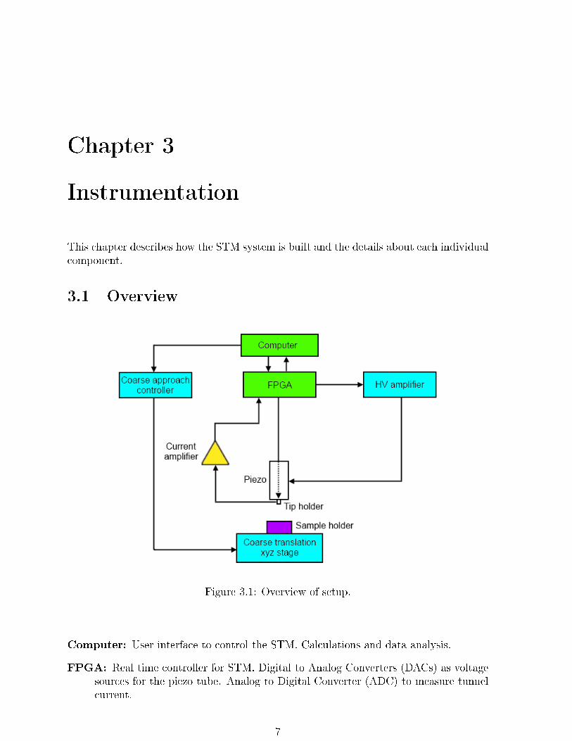
3.1 Overview
Figure 3.1: Overview of setup.
Computer: User interface to control the STM. Calculations and data analysis.
FPGA: Real time controller for STM. Digital to Analog Converters (DACs) as voltagesources for the piezo tube. Analog to Digital Converter (ADC) to measure tunnelcurrent.
7
HV amplier: Amplies the output voltage from the FPGA to the piezo tube.
Piezo: Moves the tip in xyz with a sub-nanometer resolution.
Tip holder: A small metal tube where the tip is inserted.
Current amplier: Amplies the tunneling current to a measurable quantity for theFPGA.
Coarse approach controller: Controls the piezo motor used for coarse approach.
Coarse translation xyz stage: Provides coarse adjustment of the sample position.Manual for lateral motion and motorized for z motion.
Sample holder: Where the sample is placed. A small spring keeps the sample stable.
3.2 Piezo Tube
The piezo tube plays a central role in the microscope. It works as an actuator and makesit possible to move the tip across the sample with high resolution and hence perform ascan. The tube does not only move in the lateral direction but also in the axial direction.This is crucial for the height control of the tip during scan and also for the initial approachto the surface. Having the possibility to control 3D motion with just one component isconvenient and saves space in the setup.
3.2.1 Properties
A piezoceramic material, such as lead zirconium titanate (PZT), changes shape when anelectrical eld is applied. This is usually done by applying a voltage across electrodesattached to the material. Depending on how the electrodes are positioned dierent partsof the material will be subject to the emerged electric eld, making it possible to elongatethe piezoceramic in the desired direction. As high electric elds applied correspondsto tiny changes in shape, a high resolution can be obtained, sub-nanometer, which isessential for atomic imaging.
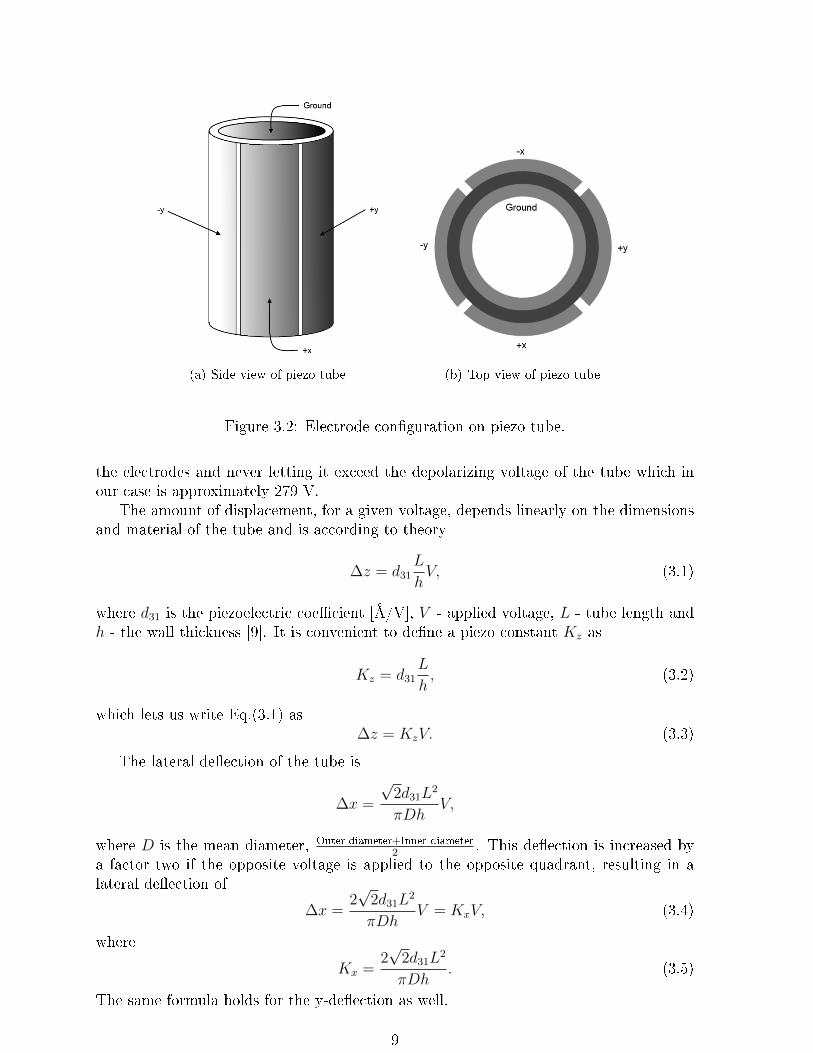
For the STM in this experiment we use a piezo tube with quartered electrodes onthe outside, as can be seen in Fig. 3.2, and one large cylindrical electrode on the insideserving as ground plane.
The four separate electrodes on the outside enable control of motion in ±x and ±ybut can also be used for axial displacement. By applying the same voltage on all fourquadrants the tube will be displaced in z direction. In practise it is dicult to applyexactly the same voltage on all four electrodes since they are connected to separateampliers which are not identical to each other. This introduces errors both in lateraland axial movement of the tube which is not desirable. However, there is another wayto control the z displacement more accurately. The inside of the tube, serving as groundfor the outer electrodes, can also be used for the axial motion. Applying a voltage onthe inner electrode is eectively the same as applying a voltage on all outer electrodesbut with opposite sign. This way the axial motion can be controlled without having touse the outer electrodes, allowing separate control of deection and displacement of thetube. When using this method it is important to keep track of the total voltage across
8
(a) Side view of piezo tube (b) Top view of piezo tube
Figure 3.2: Electrode conguration on piezo tube.
the electrodes and never letting it exceed the depolarizing voltage of the tube which inour case is approximately 279 V.
The amount of displacement, for a given voltage, depends linearly on the dimensionsand material of the tube and is according to theory
∆z = d31L
hV, (3.1)
where d31 is the piezoelectric coecient [Å/V], V - applied voltage, L - tube length andh - the wall thickness [9]. It is convenient to dene a piezo constant Kz as
Kz = d31L
h, (3.2)
which lets us write Eq.(3.1) as∆z = KzV. (3.3)
The lateral deection of the tube is
∆x =
√2d31L
2
πDhV,
where D is the mean diameter, Outer diameter+Inner diameter
2. This deection is increased by
a factor two if the opposite voltage is applied to the opposite quadrant, resulting in alateral deection of
∆x =2√
2d31L2
πDhV = KxV, (3.4)
where
Kx =2√
2d31L2
πDh. (3.5)
The same formula holds for the y-deection as well.
9
The tube used in this experiment is 1 inch long (2.54 cm), 0.5 inch outer diameter(1.27 cm), wall thickness of 1
16inch (0.1588 cm), D = 0.4375 inch (1.1112 cm) and has
a piezoelectric coecient d31 of -2.15 Å/V. Plugging these numbers into equations (3.2)and (3.5) yields
Kz = −34.4 Å/V (3.6)
andKxy = −70.79 Å/V (3.7)
which are the theoretical piezo constants for our piezo tube.
3.3 Sample stage
The sample stage used in the experiment is a MicroBlock 3-Axis Flexure Stage fromThorlabs. It has manually adjustable x and y axes while the z axis is driven by aSquiggle piezoelectric step motor which we will discuss in more detail in the next section.
The stage has been slightly modied in the earlier work by Sergiy Cherepov who usedit for CIPT measurements [4]. With some additional parts and adjustments the stage isadapted to support our STM.
The whole set-up is placed on a TS-150 stable table from Table Stable Ltd whichactively reduces low frequency vibrations which might aect the performance of theSTM and also the quality of the results. The stable table stands on an optical tablewhich reduces vibrations from the building as a rst safety measure.
3.3.1 Squiggle piezo motor
The piezo tube only has an axial range of approximately 0.5 µm. Therefore, a coarseapproach needs to be done to get the piezo tube within range from the sample surface.For this kind of approach a longer range is more important than high resolution.
What we use in the set-up for coarse approach is a piezoelectric motor called "SQUIG-GLE" from New Scale Technologies' SQ-100 Series [10]. It is designed for nanopositioningapplications. The SQUIGGLE motor is non-magnetic and has a range of 50 mm and aresolution up to 20 nm, which meets our requirements. It comes with a usb motor con-troller which can be controlled with the supplied software or with ActiveX commandsand is therefore easily incorporated in a LabVIEW program.
10
3.4 Scanner head
When building the scanner head of the STM the tip holder needs to be attached to thepiezo tube which itself needs to be secured somewhere. Piezo electrodes must be wiredto the HV amplier and the tip requires a proper electrical contact to the pre-amp.
Figure 3.3: 3D-view of complete probe mount. Purple is piezo tube.
3.4.1 Tip holder
When designing the tip holder we have a few requirements: Ability to easily change thetip, has to t on the piezo tube, needs to be non-conducting and to support our groundingmethod. We decide to make a plug-resembling piece which goes onto the bottom of thepiezo tube, see Fig. 3.4. The piece is made out of Macor, a glass-ceramic material whichcan easily be machined into any shape [11]. It is electrically non-conducting and alsoa good thermal insulator with very little expansion due to temperature changes. Thecenter hole is big enough to t an MMCX female receptacle which will serve as the actualtip holder. The receptacle is a small metal tube with an inner wall in the middle, dividingit into two parts. This makes it easy to solder a cable in one end leaving the other forinserting a tip. The four other holes on the piece make our grounding method possible.
The Macor piece is glued to the piezo tube with epoxy, a two-component adhesivewhich forms a strong polymer with high temperature resistance.
11
Figure 3.4: 3D-, side- and top view of tip holder.
3.4.2 Piezo tube holder
To x the piezo rigidly we design a plate, also in Macor, with a hole in the center havingthe same diameter as the tube. In this hole the tube is glued with epoxy s such that itstop edge is in height with the plate surface. Around the center hole four smaller holesare made, large enough to pull through wires to the outer electrodes on the piezo tube.In the corners of the plate four screw holes are made so that the plate can be attachedto the sample stage.
Figure 3.5: 3D-, side- and top view of piezo tube holder.
12
3.4.3 Cabling
RF compatibility
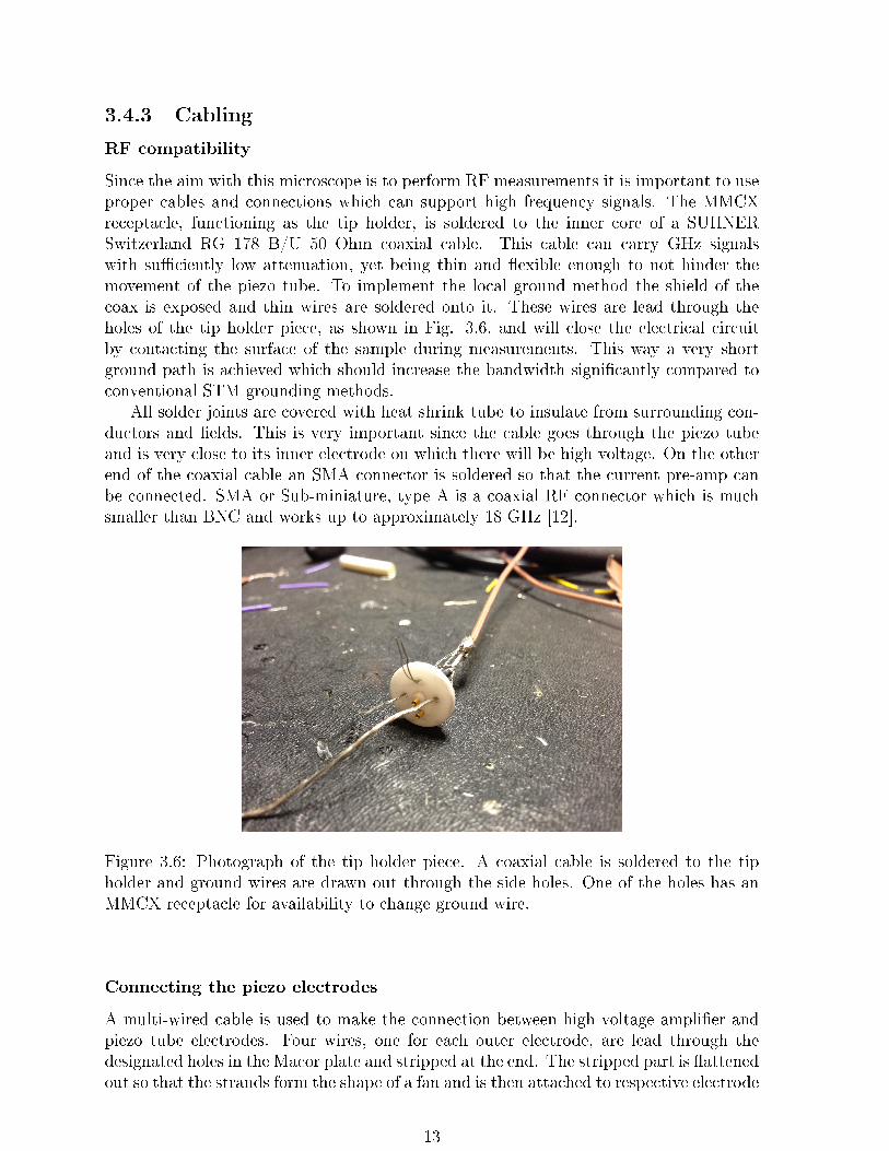
Since the aim with this microscope is to perform RF measurements it is important to useproper cables and connections which can support high frequency signals. The MMCXreceptacle, functioning as the tip holder, is soldered to the inner core of a SUHNERSwitzerland RG 178 B/U 50 Ohm coaxial cable. This cable can carry GHz signalswith suciently low attenuation, yet being thin and exible enough to not hinder themovement of the piezo tube. To implement the local ground method the shield of thecoax is exposed and thin wires are soldered onto it. These wires are lead through theholes of the tip holder piece, as shown in Fig. 3.6, and will close the electrical circuitby contacting the surface of the sample during measurements. This way a very shortground path is achieved which should increase the bandwidth signicantly compared toconventional STM grounding methods.
All solder joints are covered with heat shrink tube to insulate from surrounding con-ductors and elds. This is very important since the cable goes through the piezo tubeand is very close to its inner electrode on which there will be high voltage. On the otherend of the coaxial cable an SMA connector is soldered so that the current pre-amp canbe connected. SMA or Sub-miniature, type A is a coaxial RF connector which is muchsmaller than BNC and works up to approximately 18 GHz [12].
Figure 3.6: Photograph of the tip holder piece. A coaxial cable is soldered to the tipholder and ground wires are drawn out through the side holes. One of the holes has anMMCX receptacle for availability to change ground wire.
Connecting the piezo electrodes
A multi-wired cable is used to make the connection between high voltage amplier andpiezo tube electrodes. Four wires, one for each outer electrode, are lead through thedesignated holes in the Macor plate and stripped at the end. The stripped part is attenedout so that the strands form the shape of a fan and is then attached to respective electrode
13
with silver paint. The silver paint forms a sturdy junction when it hardens and providesa good electrical connection between wire and electrode. It is not as robust as a solderjoint but soldering on a piezoelectric material always comes with the risk of depolarizingit if the temperature exceeds the Curie temperature [13].
The inner electrode is connected in the same way using a fth wire from the multi-wired cable. The cable is xed to the Macor plate with a clamp such that the electrodewires are secured without tension. At the other end a D15 connector is soldered with thepins matching the corresponding outputs on the HV amplier.
3.5 STM circuitry
3.5.1 Current pre-amplier
The tunneling current typically ranges from 10 pA to 10 nA and to be able to measure thiscurrent it needs to be amplied. A transimpedance amplier circuit is a good choice forthis task because it converts an input current to a voltage which can easily be measuredby the controller device.
Circuit theory
The transimpedance amplier circuit is an operational amplier (op-amp) with negativefeedback, as can be seen in Fig. 3.7(a). In an ideal op-amp no current goes throughit because the resistance between the inputs is innite. In reality this resistance is notinnite but still very high. The resistor R in our circuit is a 100 MΩ resistor, which issmall compared to the internal resistance of the op-amp, and hence all the current will gothrough it. As the current goes through the resistor a voltage drop will occur. What theop-amp does is adding a voltage to the input source to compensate for the drop over theresistor and therefore keeping the dierential input voltage at zero. The closed loop gainis easily determined as VOUT = −IINR. What we also need to consider in this circuit is
(a) Basic transimpedance amplier circuit. (b) Transimpedance amplier circuit with tunnel junc-tion as current source. The voltage applied on thepositive input will yield a bias voltage over the tunneljunction.
Figure 3.7: Schematic over transimpedance amplier circuit.
the bias voltage which is going to be applied over the tunnel junction. By inserting a
14
voltage source, VB, at the positive input of the op-amp, instead of ground, the potentialis raised (See Fig. 3.7(b)). Since the amplier keeps the dierential input voltage at zerothe potential will also be raised at the negative input, which leads to a bias voltage overthe tunnel junction. By introducing this voltage source we also aect the output of theamplier. The voltage going out will have an oset equal to the bias voltage
VOUT = −IINR + VB. (3.8)
Building the amplier
In our circuit we use an LF411 operational amplier from National Semiconductor Cor-poration. It has a fast response time, less than 1 µs for a 10 V output voltage swing [14].The typical swing when scanning is much lower than this value and what actually limitsthe measuring speed in the STM is not the op-amp but the FPGA which has samplingperiod of 5 µs.
The op-amp requires a DC supply voltage and the performance of the amplier de-pends on how stable this supply voltage is. An ideal voltage source would lead to anoutput only governed by the input. By using batteries as power supply, two 9 volt batter-ies in this case, the voltage will remain very stable and therefore increase the quality ofthe amplier output. To prevent the batteries from running out when the amplier is notbeing used a switch is installed which can open and close the connection to the op-ampsocket. The batteries are also grounded to the box and the last component installed isthe 100 MΩ feedback resistor
3.5.2 High voltage amplication
As the piezo tube requires high voltages in order to achieve a large displacement ordeection, the output from the FPGA card needs to be amplied. The ±10 V analogoutput would only correspond to a lateral deection, or scan range, of ±70.79 nm, whichis not sucient for our purposes.
In this project we use an amplier made in earlier work by Sergiy Cherepov [4]. Ithas the capacity of amplifying ve separate channels, which is what we need for the piezotube electrodes. The amplier input connector is a male D25 and the output is a femaleD15.
The amplication on the ve separate channels is determined by applying dierentvoltages to the amplier and reading out the output voltage with a multimeter. Theway we applied the voltages to the amplier was by writing a small LabVIEW programwhich output a voltage corresponding to a certain bit-value. This way we obtain theoutput voltages from the amplier as functions of bit-values in the FPGA, which in theend is necessary to know to control the piezo tube. By plotting the data we retrieved(see Fig.3.8) we could clearly see a linear region in every channel as expected. Thenonlinear parts in the beginning and end of every curve is where the saturation limit ofthe amplier is reached and will not be used during operation. A linear t of the datafrom each channel gives the conversion coecients between amplier output and FPGAoutput, which are necessary for being able to apply the desired voltage to the piezo tube.Results are summarized in table 3.1.
15
−3 −2 −1 0 1 2 3
x 104
−150
−100
−50
0
50
100
150
FPGA output voltage [bit]
Am
plif
ier
ou
tpu
t [V
olt]
AO0
AO1
AO2
AO3
AO4
Figure 3.8: FPGA output voltage dependence of the amplier output.
Table 3.1: Coecients for converting FPGA analog output to high voltage amplieroutput.
3.5.3 Voltage spike protection
When using high voltages there is always the risk of damaging sensitive equipment whichuses low voltages, like logic devices. The FPGA-card is directly connected to the highvoltage amplier and is therefore vulnerable to voltage spikes caused by malfunction. Thispotential problem is easily prevented by putting Transient-Voltage-Suppression diodes(TVS diodes) in the circuit [15].
A TVS diode is a clamping device that shunts the excess current when the voltageexceeds a certain level. Below this level the diode is in principle invisible and will notaect the circuit. By putting a diode in parallel with signal and ground, see Fig. 3.9,any voltage spike will result in a current going to ground, clamping the voltage at a safelevel.
There are a few denitions (also shown in Fig. 3.10 )used when specifying the char-acteristics of a TVS diode:
• Stand-o voltage (VRM): The voltage below which no signicant current isshunted.
• Breakdown voltage (VBR): The voltage when some specied and signicant
16
Figure 3.9: How the TVS diode is put in the circuit to protect from voltage spikes.
current is shunted.
• Clamping voltage (VCL): The voltage at which the diode will conduct its fullyrated current.
These denitions are important to know in order to choose the correct diode for yourcircuit. In our case we wanted the FPGA to unhindered be able to output its full range,i.e. voltages between +10 V and -10 V. Therefore the stand-o voltage should be 10 Vminimum, otherwise the diode would reduce the output range of the FPGA. Voltagesoutside this range are essentially undesired and might harm the electronics. The FPGAcard has a built-in protection system but it only works up to 42 V and a voltage spike fromthe high voltage amplier could in principle be much higher. This suggests a maximalclamping voltage of 42 V. We chose a diode from MULTICOMP called P6KE12CA withVRM = 10.2 V and VCL = 16.7 V which suits our needs.
Figure 3.10: Electrical characteristics of a bidirectional TVS diode. Image from STMi-croelectronics [16].
17
3.6 FPGA
A Field-Programmable Gate Array (FPGA) is a chip which can be programmed to desiredapplication, e.g. Digital Signal Processing (DSP). Unlike "Application Specic IntegratedCircuits" (ASICs) an FPGA can easily be reprogrammed after manufacturing and is notdesigned for one specic task [17] [18]. This exibility is very useful for a developer whomight need to change the functionality often.
FPGAs have several advantages compared to conventional CPU-based systems. AnFPGA chip is only processing logic and do not have an operating system which canintroduce delays and interruptions. This is crucial when it comes to real-time control ofa sensitive system, which the STM is. Furthermore, the speed of an FPGA is not limitedby number of processor cores like a CPU. Each independent processing task in the FPGAhas its own dedicated section on the chip. Depending on the memory size of the FPGAmany processes can be done in parallel [19]. The chip also contains I/O blocks whichallows the circuit to interact with the outside world through DACs and ADCs.
The FPGA we use is a PCI-7833R card from National Instruments. It has: 8 analoginputs with independent sampling rates up to 200 kHz (5 µs sampling period), 16-bitresolution and ±10 V range. 8 analog outputs with independent update rates up to 1MHz, 16-bit resolution, ±10 V range. 96 digital lines for inputs or outputs at rates upto 40 MHz. The FPGA is programmable with the LabVIEW FPGA module which wewill discuss more in the next section.
3.7 Software
3.7.1 LabVIEW basics
As mentioned earlier the FPGA is programmed and compiled in LabVIEW which isa development platform with the purpose of programming and automating measuringinstruments in a lab environment. LabVIEW is based on a graphical programminglanguage which lets the user create programs without any knowledge about conventionalcode languages. A LabVIEW program, called virtual instrument (VI), consists of twocomponents: a front panel and a block diagram. The front panel is the user interfacewhere controls and indicators are placed for data input and output respectively. They willappear as terminals in the underlying block diagram which contains the graphical sourcecode. The control terminals are wired to function-nodes in order to perform operationson the input data and then wired to indicator terminals to display the result.
3.7.2 LabVIEW FPGA module
Programming an FPGA is dierent from other LabVIEW applications in many aspects.In general you have one main VI which is in charge of linking all smaller building blockstogether to form a program. Programming an FPGA requires two VIs: A target VI,which contains the code which is going to be executed on the FPGA, and a host VI whichis the program on the computer that communicates with the FPGA. These, somewhatspecial, conditions require careful planning of what to put in which VI. Some tasks aremore desirable, or even necessary, to have in one of the two. All critical processes whichneed real-time control without interruptions should be placed in target. In our case
18
this applies to approach, scan and feedback. Even so, it is important to not put anyavoidable calculations or data storage on the FPGA since it has a limited memory sizewhich is easily exceeded. The host takes care of everything that is not so critical, suchas converting user input to complete instructions for the FPGA, data collecting andprocessing, presentation of results.
Host VI
The host VI is the interface to the user. It lets the user set parameters like piezoproperties, measurements rates, step sizes, current setpoint, scan size etc. It also containscontrols for running the dierent parts of the program, such as approach, scan and manualsquiggle control. For example, pushing a button triggers an event structure in the blockdiagram which holds the code responsible for that task.
Within the host VI a reference to the target VI is made. This reference is usedthroughout to program to communicate with the FPGA. Connecting a Read/Write nodeto the reference gives access to the controls on the target's front panel and is typicallyused when timing is not important, e.g. setting scan parameters.
Target VI
In this subsection we will highlight what is dierent when programming the FPGA. Thetarget VI is essentially invisible to the user, it is the "machine room" of the programwhere user commands are translated to real action. Programming the target is dierentfrom programming a normal VI. This is because the code is executed on the FPGA whichhas more restrictions and fewer compatible functions to use, mostly due to the limitedmemory size.
FPGAs use binary coding and with that the 16-bit output/input voltages are con-verted from/to binary values. The 16-bit analog output/input range is [-10, 10] V andhence, the voltage bit-conversion is given by
Voltage =Output Code
32768× 10.0V. (3.9)
FPGAs use integer math for calculations and cannot process oating-point numberseciently. To get around this problem xed-point numbers (FXPs) and FXP functionscan be used. FXP numbers are essentially represented by a number of bits which is veryconvenient for the FPGA logic to handle. They have a user-dened range and precisionwhich allows less memory to be occupied on the FPGA than with oats.
A process, such as scanning, can generate a vast amount of data, in a short periodof time, which might be too much for the FPGA to store. This problem is solved bytransferring the data from the FPGA to the host, using a "First In, First Out" (FIFO)buer memory. The FIFO memory gives the host time to fetch data without stalling thedata storage process in the target, as long as the buer does not get full.
Arrays should in general be avoided in the target since they require a lot of space.Also, they do not have the same exibility as in normal computer VIs where arrays canbe resized, appended etc. Target arrays must have predetermined lengths at the time ofcompilation and is therefore not very useful in dynamic processes.
Since the target has to be compiled after each change it is also advantageous touse variables instead of constants in the FPGA because they can be changed duringexecution.
19
3.7.3 Approach algorithm
The approach mechanism is a combination of coarse approach with the SQUIGGLE andne approach with the piezo tube. First the piezo tube is stepwise swept from fullycontracted to fully expanded. In between each step the tunneling current is measuredand averaged, 10 samples with a sampling period of 5 µs. If the mean value is above orequal to the current setpoint the approach is completed or stopped. If the piezo tube hasexpanded fully without getting into tunneling distance the SQUIGGLE motor needs tobe stepped. However, the SQUIGGLE is controlled with an ActiveX component whichcan not be called from the target. A signal needs to be sent to the host telling it to stepthe SQUIGGLE. Before doing this the piezo is reset to a fully contracted state, preparedfor a new "piezo sweep". The target VI sends an interrupt request (IRQ) to the host.This IRQ stops the execution in the target until the host has responded on this request.Meanwhile the host listens for this IRQ and is programmed to step the SQUIGGLE whenit obtains the signal. After the SQUIGGLE is stepped a response is sent back to thetarget, telling it to continue approach with the piezo again. This closes the loop whichis iterated until approach is complete.
To summarize the approach algorithm:
1. Step piezo
2. Measure current
3. Iterate until setpoint is reached or piezo is fully expanded
4. If fully expanded, reset piezo and take a coarse step with SQUIGGLE
5. Repeat these steps until current setpoint is reached
The approach also serves another important purpose - determining the exact expo-nential relation between distance and tunneling current. By recording data from theapproach it is possible to see exactly how the current behaves as a function of z piezovoltage. Fitting of the model to this approach data yields the parameters and a mathe-matical expression for the current as a function of output voltage [bits], which we wantto use in the feedback algorithm.
3.7.4 Feedback algorithm
As we discussed earlier it is desirable to scan in constant current mode when having arough sample. To keep the current constant it is necessary to have a feedback loop thatadjusts the height based on the error signal, i.e the deviation between measured currentand setpoint. Since we already know from the approach how the current behaves as afunction of distance (corresponding to piezo voltage)
I = ae−bz (3.10)
where a and b are unknown parameters. We can use this relation to make a very precise,model-based, controller. However, it is important to notice that the approach curve maynot be static since the tip-sample separation depends on more things than piezo voltageonly. Drifts and noise will alter the tunneling current even though the piezo voltage is
20
kept constant. These drifts will manifest themselves as a time-dependent shift of theapproach curve. This is graphically depicted in gure 3.11 where the original approachcurve (blue) has been shifted by a constant, c, to the position of the green curve.
I = ae−bz → I ′ = ae−b(z+c), c ∈ R.
If a current setpoint is dened as I0 we have I0 = I(z0). A drift would mean that thecurrent at the same piezo voltage changes to I ′(z0) = I1. To account for this drift thepiezo voltage needs to be adjusted back to I0 which is now located at z1. The adjustment∆z can be expressed in known terms
∆z = z1 − z0
= −1
bln
(I0a
)− c− z0 (3.11)
The constant c is solved for using the second current measurement
I1 = ae−b(z0+c) ⇒ c = −1
blnI1a− z0 (3.12)
which then can be substituted into Eq. (3.11)
∆z = z1 − z0
= −1
bln
(I0a
)− c− z0
= −1
bln
(I0a
)−
(−1
blnI1a− z0
)− z0
=1
bln
(a
I0
)+
1
blnI1a
=1
bln
(I1I0
).
And using the relation between distance and piezo voltage (Eq. (3.3)) we can write this
∆z = Kz∆V =1
bln
(I1I0
). (3.13)
It turns out that the only parameter necessary for the feedback to work is b.In principle this feedback method should be very robust. However, there are limi-
tations in the hardware which introduce sources of error. First of all there is an upperlimit in the tunneling current that can be measured. The current pre-amplier will notbe able to output a voltage higher than its internal power supply, which in this case is 9V and corresponds to 90 nA tunneling current. If this limit is reached the actual currentcan not be determined and the feedback might not be able to adjust the piezo sucientlyin one step. However, it will make its maximum adjustment and decrease the currenttowards the setpoint.
If the maximum output of the pre-amp is exceeded there is a chance that the tip willcrash. To reduce the risk of this happening we used a fairly high bias voltage, 500 mV,which means that a tunneling current will appear further away from the surface thanwith a lower bias voltage (see Eq. (2.1)).
21
A similar problem arises if the current gets too low. Since the current is exponentiallydecreasing with distance it goes to zero rapidly. The FPGA has a nite resolution andthe smallest voltage it can read out corresponds to 0.3 mV. If the current goes below thisvalue the tip is not within tunneling distance any more but there is no way to know howfar away it is. The largest step down might not be enough to get into tunneling again.
Piezo voltage
Tu
nn
elin
g c
urr
en
t
z1 z0
I0
I1
Original curve: ae−bz
Drifted curve: ae−b(z+c)
Figure 3.11: Graphical description of how drift aects the tunneling current.
3.7.5 Scan algorithm
There are essentially three parameters for the user to set before making a scan: Scansize, step size (resolution) and measuring time per pixel. The host converts the sizeparameters to bit values and sends them to the target.
The scan pattern used is a raster pattern - a series of rows covering a rectangulararea as can be seen in Fig. 3.12. Each row the probe is moved from left to right (trace)and then back (retrace), ending up where the row started. Since the feedback introducesdierent artefacts when the tip goes up or down a steep edge, more information is obtainedwhen scanning in both directions. It also makes it possible to measure how much driftthere is because the same pixel is measured twice with some time in between. The scanalgorithm consists of two loops - one inner loop for the fast scan direction and one outerfor the slow. It is programmed such that scanning a row is an independent function whichis called several times to build up the whole scan. At each pixel the tunneling currentis measured after which the feedback adjusts the tip-height accordingly, before the tip ismoved to the next pixel. The height-data for each pixel is sent to the host through theFIFO buer.
Now the fast scan loop is closed and is iterated as many times as there are pixels ina row. At this point the outer loop has performed one whole iteration and the process
22
Figure 3.12: Illustration of the scan pattern used.
is repeated as many times as there are rows. When scan is nished the target sends asignal to the host to notify the completion.
3.8 Tip preparation
In order to have a functioning STM a sharp, conducting tip is required. STM tips areusually made from tungsten or Pt/Ir alloy which are sti, chemically stable and do notoxidize in air. Oxidization of the tip might lead to a deterioration in the tunnelingcapability of the microscope. However, at this stage of the project we stuck to simple,easy to make, copper wire tips which is enough for our purposes.
There are essentially two methods when it comes to preparing STM tips; Electro-chemical etching and cutting [20]. The etching method produces sharper tips with higheraspect ratio but requires more work. Such tips might be necessary when imaging highlyproled surfaces. If there is no need for high aspect ratio the cutting method is easierto do and still yields atomically sharp probes. The cutting method is really simple andonly requires a pair of wire-cutters. The wire is cut at a 45 degree angle while simulta-neously pulling it. The stretching force will cause a plastic deformation of the wire andwill produce a small extended apex at the tip, as can be seen in gure 3.13. This apexhas a radius in the order of 100 nm, which is very good for such a primitive preparationmethod.
23
(a) Plastic deformation of the tip can be seenwhere the cut was made.
(b) Closer view of the tip.
(c) View of the outermost part of the tip. (d) Tip apex.
Figure 3.13: SEM-images of cut tip.
24
Chapter 4
Experimental results and discussion
4.1 Actual Piezo Displacement
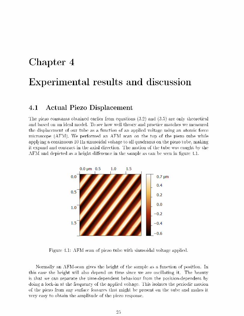
The piezo constants obtained earlier from equations (3.2) and (3.5) are only theoreticaland based on an ideal model. To see how well theory and practice matches we measuredthe displacement of our tube as a function of an applied voltage using an atomic forcemicroscope (AFM). We performed an AFM scan on the top of the piezo tube whileapplying a continuous 10 Hz sinusoidal voltage to all quadrants on the piezo tube, makingit expand and contract in the axial direction. The motion of the tube was caught by theAFM and depicted as a height dierence in the sample as can be seen in gure 4.1.
Figure 4.1: AFM scan of piezo tube with sinusoidal voltage applied.
Normally an AFM-scan gives the height of the sample as a function of position. Inthis case the height will also depend on time since we are oscillating it. The beautyis that we can separate the time-dependent behaviour from the position-dependent bydoing a lock-in at the frequency of the applied voltage. This isolates the periodic motionof the piezo from any surface features that might be present on the tube and makes itvery easy to obtain the amplitude of the piezo response.
25
Determining the piezo motion amplitude as a function of the voltage amplitude is donein a few steps: First the height prole of each line of the scan image is obtained. Theperiodic behaviour is clearly visible which can be seen in Fig. 4.2(a). When having theheight data for a line a fast Fourier transform (FFT) is performed, yielding a spectrumsimilar to the one in Fig. 4.2(b). The peak is located at 10 Hz as expected since the
(a) Height prole. (b) FFT of height prole.
Figure 4.2: Height prole from one line of the AFM-scan and the corresponding amplitudespectrum.
drive frequency is 10 Hz and since there is a linear response. The height of the peakcorresponds to the amplitude of the oscillation, which is the value of interest for us.
Doing an FFT on all lines of the scan, typically 256, and taking an average of all thecollected amplitudes gives an estimation of the displacement as a function of voltage. Wedid this procedure with dierent voltage amplitudes to see the overall behaviour and toobtain a more accurate result in the end. A linear t of the data was made, see gure 4.3,in order to obtain the slope, which corresponds to the axial piezo constant. Comparingthis value to the one we obtained from the theoretical model, Eq. (3.6), shows a smalldierence. The experimentally determined value seems to be a little smaller than thetheoretical one. This is most likely because of the way we xed the piezo tube to theprobe mount, reducing the eective length of the tube. Another cause could be the tipholder and cable adding a weight load to the the tube and therefore decrease the abilityto expand.
26
0 50 100 150 2000
100
200
300
400
500
600
Piezo voltage [V]
Pie
zo d
ispla
cem
ent [n
m]
Data
Linear fit
Slope: 3.2918 nm/V
Figure 4.3: Linear t of the experimentally obtained piezo displacement as a function ofapplied voltage.
27
4.2 Approach
Before running the automated approach algorithm some manual preparations are done.A copper tip is made, using the cutting method described earlier, and placed in the tipholder. A gold sample is mounted on the stage and positioned below the tip. At thispoint the distance between tip and sample is in the order of centimetres and would takehours to approach automatically. With the use of an optical microscope the gap canbe decreased manually, by stepping the SQUIGGLE, to a point where the separation isonly a few tens of micrometer. From here the approach algorithm can do the rest ofthe approach within a few minutes. A plot of the approach data, see Fig. 4.4, shows
0 50 100 150 200 250−200
0
200
400
600
800
1000
1200
Piezo voltage [bits]
Curr
ent [b
its]
Measurement data
Excluded data
Exponential fit
Figure 4.4: Exponential t of the tunneling current as a function of piezo voltage.
the exponential behaviour of the current as a function of distance which can only beexplained by the quantum nature of the electrons. This result shows that it is possible toget into tunneling distance with the STM, an important step towards scanning. As wesee in the gure the current goes from 0 to 1000 bits in approximately 100 bits outputvoltage at 500 mV bias voltage. These values correspond to a tunneling current from 0to 3.05 nA in approximately 3.16 nm change in distance, which is quite high compared toothers work. The reason for this is most likely the relatively large tip radius, caused bythe somewhat primitive tip preparation method, which increases the amount of tunnelingelectrons and therefore also the current.
Fitting equation (3.10) to the data obtained from the approach yields the value of theparameter b, which we need to have in order to make the model-based feedback to work,see Eq. (3.13). In this specic approach a b-value of approximately 0.04 was obtained, a
28
value which several other approaches also yielded.
4.3 Scan
When testing the scan it is necessary to know what results to expect in order to evaluatethe performance. Therefore, all scans in this thesis are made on a reference sample withknown characteristics - an SPM calibration pattern. It is a gold sample with a matrix ofetched down squares with a size of 500× 500 nm and periodicity of 1 µm.
4.3.1 Lateral deection
By scanning the calibration pattern the actual piezo movement can be determined andcompared to the theoretically calculated deection. Figure 4.5 shows a scan which ac-cording to theory should correspond to 1.2× 1.2 µm. A lateral step size of 5 nm is usedand the current is measured and averaged over 40 µs per pixel. Based on the scan imagethe side of a square is approximately 450 nm. This value is within 10% of the actualvalue (500 nm) and implies that the estimated deection is quite accurate.
Figure 4.5: STM scan of reference sample. Scale is in nm.
29
4.3.2 Trace-Retrace comparison
Comparing trace and retrace image, Fig. 4.6, can reveal a lot of information. As wediscussed earlier it makes it possible to determine how much drift there is during scan.Furthermore, parachuting eects due to slow feedback are scan direction dependent andcan "smear out" the imaging of sharp drops in the sample. By looking at the scan imagefrom the opposite direction this smearing will not be visible since the tip was going upthe steep edge instead.
On a more basic level, comparing the two images gives a good perception on howreliable the scan is. If the two images match each other it is less likely that randomerrors have corrupted the result. Even so, systematic errors may still exist.
Trace height [nm]
1 µm
1 µ
m
0
95
(a)
Retrace height [nm]
1 µm
1 µ
m
0
90
(b)
Figure 4.6: Comparison of trace and retrace images taken with the STM.
4.3.3 Impact of dierent measuring times
We also want to know how the image quality is aected by dierent time of measuringof the tunneling current per pixel. It is desirable to have short time-per-pixel since itwould decrease the total scan time. However, the quality must be high enough to beable to distinguish nanopillars. The results of scans with dierent time-per-pixel aresummarized in gure 4.7. All ve scans are made consecutively at the same conditions.The lateral step size is 5 nm and the scan size is 1 × 1 µm. It seems like the reductionin time-per-pixel leads to the walls (between the squares) to appear wider. This mightbe a parachuting eect due to less accurate feedback, caused by a shorter measuringtime, when the tip moves over the wall edge. However, this is only a guess and furtherinvestigations are necessary for determining the actual cause.
30
Height [nm](time/pixel=10000 µs)
1 µm
1 µ
m
−130
168
(a)
Height [nm](time/pixel=5000 µs)
1 µm
1 µ
m
27
125
(b)
Height [nm](time/pixel=2500 µs)
1 µm
1 µ
m
−21
61
(c)
Height [nm](time/pixel=1000 µs)
1 µm
1 µ
m
164
257
(d)
Height [nm](time/pixel=500 µs)
1 µm
1 µ
m
184
273
(e)
Figure 4.7: STM scan images of the reference sample with dierent times per pixel.
31
4.3.4 Impact of dierent resolution and measuring times
Scan resolution is another factor which aects the total scan time. Decreasing the lateralstep size by a factor of two should certainly result in a more detailed image but would alsolead to a four times longer scan duration. This prolongation can however be compensatedfor by reducing the time-per-pixel by a factor of four and still yield a higher quality thanbefore. In gure 4.8 we see images from three dierent scans where these two parametersare varied. Judging by the images a higher quality is obtained when the 25 Å step size
Height [nm](time/pixel=1000 µs
xy−step=50 Å)
1 µm
1 µ
m
0
79
(a)
Height [nm](time/pixel=1000 µs
xy−step=25 Å)
1 µm
1 µ
m
0
95
(b)
Height [nm](time/pixel=250 µs
xy−step=25 Å)
1 µm
1 µ
m
0
90
(c)
Figure 4.8: STM scan images of the reference sample with dierent times per pixel.
is used compared to 50 Å. As we discussed earlier this has the cost of a four times longerscan duration. Remarkably, when also decreasing the time-per-pixel a factor of four theresult is an image with higher quality than the rst one, even though the total scan timeis the same.
32
Chapter 5
Conclusions
In this thesis we have constructed a fully functional STM, capable of locating nano-sizedfeatures on a surface. We have also presented a design for a local grounding methodallowing high frequency measurements, which remains to be evaluated. The work done isthe rst step in the development of an RF-STM with the ability to accomplish nanometer-localized high frequency transport measurements.
In this work much time was devoted to understanding and evaluating the electronicand mechanical components of the STM, in order to motivate the choice of specicimplementations, understand their limitations, and utilize them properly. The beautyof applied physics is the opportunity to combine theoretical and practical work. Forexample, circuit analysis had to be used when designing the amplier for the tunnelingcurrent and soldering skills were required to build it. Furthermore, the piezoelectricitytheory was used to determine the properties of the actuator responsible for moving thetip, so that accurate scanning could be done. These properties were also measuredexperimentally and showed good agreement with the theoretical models. The initial useof the four outer electrodes of the piezo tube for the axial movement had the advantageof reducing the number of high voltage channels but introduced a source of error whenhaving to mix axial and lateral voltages. This conguration made it very dicult to applythe same voltage at the same time on all four electrodes and resulted in a malfunctioningscan, with distortions in the image. The problem was solved by using the inner electrodeas an adjustable ground (at the cost of one more HV channel), eectively changing thevoltage on all four quadrants. Hence, the control of the axial and lateral motion wasseparated, which improved scanning.
Although a signicant amount of time has been spent on building and testing thehardware the main focus has been on developing computer algorithms for operating theSTM. It was necessary to learn how to program in LabVIEW and especially how to makeFPGA-based applications. Besides programming functioning approach and scanning al-gorithms we have implemented a model-based feedback system which uses the knownrelationship between the tunneling current and tip-sample separation to keep the currentstable. This proved to work well as long as the lateral step size was not too big, causingthe tip to loose the tunneling range - a known problem that arises with any kind of afeedback system. We found that the quality of the scans got worse if the step size was in-creased above 50 Å. Moreover, the scanning time was drastically shortened by improvingthe procedure for gathering the data and reducing the measurement time of the tunnelingcurrent per pixel, without deterioration in image quality. A long measuring time does not
33
lead to better results necessarily. It makes longer-term drifts to have a more pronouncedeect and might actually worsen the image quality. At the same time, a short measuringtime enhances the eect of high frequency noise and decreases the signal-to-noise ratio,so a trade-o had to be found. We managed to obtain images with sucient quality withmeasuring times down to 250 µs per pixel.
There is always room for improvement and a few suggestions for future work would be:Use a dierent (thinner) piezo tube to increase the maximum scan size. The current sizeof 1×1 µm is relatively small and it would be benecial to have more room for manoeuvrein cases where a particular feature on the surfaces needs to be found and investigated.Furthermore, using an MMCX receptacle as the tip holder is not very exible. It requiresthe tips to have the exact correct diameter to t and remain solidly inside. The copperwire we used for making tips had a larger diameter and had to be led o in order to tin the holder, a tedious process which did not always work. A holder with some kind ofa clip would solve this problem and would simplify tip preparation signicantly.
On the whole, the experimental results conrm the functionality of the STM andshow that we have a good basis for a continuation of the project. The fact that we haveobtained scan images reproducing the appearance of known calibration samples is theultimate proof of success.
34
Chapter 6
Acknowledgements
First I would like to express my very great appreciation to Professor Vladislav Korenivskiwho welcomed me in his research team. For teaching me the importance of criticalthinking and for sharing your valuable opinion in discussions about physics, politics,economics and community structures.
I would like to oer my special thanks to my supervisor Björn Koop for his invaluablehelp along the entire project. For your endless patience, encouragement and supportduring hard times. Thank you for giving me an insight on how scientic research is doneand for sharing your wisdom regarding life-related questions. You taught me how to seethings from a dierent perspective, a very good ability to have.
I wish to thank my closest colleague and friend Per-Anders Thorén for his pricelesssupport and encouragement. For your loyalty and for being there, sharing both successas well as adversities. Thank you for all the fun we had and for your ability to alwayscheer up my mood.
I want to thank Sergiy Cherepov for his valuable help during the beginning of thisproject. Without your expertise and your previous results my thesis would have takenmuch longer to complete.
My deepest gratitude to the members of the Nanostructure group. To Anders Lilje-borg for helping with technical issues and for sharing his vast experience in laboratorywork. To Daniel Platz, Daniel Forchheimer, Professor David Haviland and RiccardoBorgani for their indubitable will to discuss problems arising during the project.
I would also like to thank the guys I shared oce with: Motasam, Jean-Philippe andFlorian. Thank you for creating a great atmosphere and for becoming good friends.
Finally I want to express my gratitude to my family and friends for their support andendless consideration. To Therese for her innite love, support and belief in me.
35
Bibliography
[1] Sankar Das Sarma. Spintronics. American Scientist, 89(6):516, November-December2001.
[2] Salah M. Bedair, John M. Zavada, and Nadia El-Masry. Spintronic memories torevolutionize data storage. IEEE Spectrum, November 2010.
[3] D. C. Worledge and P. L. Trouilloud. Magnetoresistance measurement of unpat-terned magnetic tunnel junction wafers by current-in-plane tunneling. Applied
Physics Letters, 83(1):8486, 2003.
[4] Sergiy Cherepov. Resonant switching and vortex dynamics in spin-op bi-layers.PhD thesis, KTH, Nanostructure Physics, 2010. QC 20101209.
[5] U. Kemiktarak. Radio-frequency Scanning Tunneling Microscopy: Instrumentation
and Applications to Physical Measurements. Boston University, 2010.
[6] G Binnig and H Rohrer. Scanning tunneling microscopy. IBM J. Res. Dev.,30(4):355369, July 1986.
[9] C. J. Chen. Electromechanical deections of piezoelectric tubes with quarteredelectrodes. Applied Physics Letters, 60(1):132134, 1992. Cited By (since 1996):60.
[10] New Scale Technologies. Sq-100 series motors. http://www.newscaletech.com/
doc_downloads/SQ-100-V.pdf, December 2010. Accessed November 21, 2013.
[12] T.H. Lee. Planar Microwave Engineering: A Practical Guide to Theory, Measure-
ment, and Circuits. Number v. 1 in Planar Microwave Engineering: A PracticalGuide to Theory, Measurement, and Circuits. Cambridge University Press, 2004.
[13] Morgan Advanced Materials. Piezoelectric electrodes - soldering to silverelectrodes. http://www.morganelectroceramics.com/products/piezoelectric/piezoelectric-electrodes/, 2009. Accessed November 20, 2013.
120/LF411.pdf, April 1998. Accessed December 6, 2013.
[15] Girish Choudankar. Inexpensive solution protects sensitive devices from surges.Electronic Design, page 62, November 2012.
[16] STMicroelectronics. 1.5ke30a. http://www.st.com/web/en/resource/technical/document/datasheet/CD00000663.pdf, March 2012. Accessed October 1, 2013.
[17] National Instruments. Fpga fundamentals. http://www.ni.com/white-paper/
6983/en, May 2012. Accessed September 3, 2013.
[18] Xilinx. Field programmable gate array (fpga). http://www.xilinx.com/training/fpga/fpga-field-programmable-gate-array.htm. Accessed September 3, 2013.
[19] Renee Robbins. Advantages of fpgas. http://www.controlengeurope.com/
article/32043/Advantages-of-FPGAs.aspx, March 2010. Accessed September 5,2013.
[20] V.L. Mironov. Fundamentals of Scanning Probe Microscopy. Institute of Physics ofMicrosctructures of RAS, N. Novgorod, 2004.