72
Development of thin films of thermographic phosphors for spatial resolved temperature measurements using sputtering techniques Jhon Alexander Pareja Restrepo November 2012

Development of thin films ofthermographic phosphors forspatial resolved temperaturemeasurements using sputteringtechniquesJhon Alexander Pareja RestrepoNovember 2012

Development of thin films of thermographic phosphors for spatial resolved temperature measure-ments using sputtering techniques
Master-Thesis of Jhon Alexander Pareja Restrepo
1. Advisor: Prof. Alejandro Molina2. Advisor: Prof. Alejandro Toro

Development of thin films of thermographicphosphors for spatial resolved temperaturemeasurements using sputtering techniques
Jhon Alexander Pareja Restrepo
Thesis presented as a partial requirement to obtain the degree of:M.Sc. in Chemical Engineering
Advisor:Alejandro Molina
Co-advisor:Alejandro Toro
Research group:Bioprocesos y Flujos reactivos
Universidad Nacional de Colombia - Sede MedellínFacultad de Minas, Departamento de Procesos y Energía
Medellín, Colombia2012

Desarrollo de películas delgadas de materialesfosforescentes para mediciones de
temperatura superficial utilizando técnicassputtering
Jhon Alexander Pareja Restrepo
Tesis presentada como requisito parcial para optar al título de:M.Sc. en Ingeniería Química
Director:Alejandro Molina
Codirector:Alejandro Toro
Grupo de Investigación:Bioprocesos y Flujos reactivos
Universidad Nacional de Colombia - Sede MedellínFacultad de Minas, Departamento de Procesos y Energía
Medellín, Colombia2012

A mis padres, Olga y Guillermo, y a mis hermanos,Julián David y Andrés Fernando. Sus enseñanzas,amor, apoyo y sacrificio son los pilares de mi vida.
"Sì come una giornata bene spesa dà lieto dormire, cosìuna vita bene usata dà lieto morire".
Leonardo da Vinci
I

AcknowledgmentsI want to thank the following people and institutions that, directly or indirectly, contributed to the ac-complishment of this thesis and that somehow were involved in my master’s program.
My advisor, Professor Alejandro Molina. It has been an honor working with him. His scientific thorough-ness and tireless dedication to his students make him a model to follow. When I was lost, his supportand guidance put me always back in the right direction . He always recognized my achievements, butalso, never hesitated to invite me to drink a tinto (coffee) in the cafeteria every time that I deserved it.
My co-advisor, Professor Alejandro Toro, who with his knowledge and good sense of humor supportedme in the materials science topics.
Professor Andreas Dreizler, for giving me the opportunity of staying at the Center of Smart Interfaces ofTechnische Universität Darmstadt (TU Darmstadt) and for providing me all the necessary resources tocarry out this thesis.
Dr. Christian Litterscheid, Matthias Euler and Norman Fuhrmann, for their patience to teach me andtheir valuable contributions to this work. They were always willing to help me, not only with my re-search but with my personal issues in Germany.
Professor Barbara Albert, for allowing me using the facilities and resources of her group, at the Eduard-Zintl-Institut für Anorganische und Physikalische Chemie, to prepare the thermographic phosphors andmeasure the XRD patterns.
PD. Bernhard Kaiser and Jürgen Ziegler, for their assistance during the sputtering experiments.
Universidad Nacional de Colombia, for the complete funding of my master’s program, including my stayat TU Darmstadt, through the program "Beca Estudiante Sobresaliente de Posgrado 2011-2012".
Facultad de Minas of Universidad Nacional de Colombia - Sede Medellín and Institut Reaktive Strö-mungen und Messtechnik of the Center of Smart Interfaces, for the partial funding of my research inGermany.
My colleagues and friends from Universidad Nacional de Colombia - Sede Medellín, almost two years ofgood times. Particularly, I want to thank Astrid Ramírez and Sebastian López, for their assistance withthe time-consuming but necessary paperwork.
My colleagues and new friends from TU Darmstadt, for always trying to facilitate my life in Germany.
Last but not least. My family: my mother, Olga, my father, Guillermo, my brothers, Julius and Andrés;and my friends: Juan Fernando, Oscar, Tobón, Nery, the beautiful Juliana, Laura, Milo, Aleja, Cuevas, Di-ana Cecilia, Hugo, Andresco, Gaby, Juribo, Ivancho, Mary, Olmos, Astrid, Juanca, Jordant, Henry....Theirencouragement, support and presence, even in the distance, make me feel a very lucky person.
II

AbstractTwo thermographic phosphors materials for surface temperature measurements, praseodymium-dopedcalcium titanate, CaTiO3:Pr3+, and chromium-doped gadolinium gallium oxide, Gd3Ga5O12:Cr3+, havebeen successfully deposited on stainless steel substrates by radio frequency magnetron sputtering. Forthe sputtering process, phosphor targets were prepared using sol-gel combustion (for CaTiO3:Pr3+) andsolid-state reactions (for Gd3Ga5O12:Cr3), combined with high temperature sintering. The physical,chemical and luminescence properties of the phosphor films have been evaluated using X-ray diffraction(XRD), X-ray photoelectron spectroscopy (XPS) and laser diagnostics. The results showed that the lu-minescence features of the thin films were restored by heat treatment after the sputtering deposition.The CaTiO3:Pr3+ film showed low temperature sensitivity of its luminescence lifetime and poor pre-cision of the temperature determination, which could limit its thermographic functionality. Contrary,the Gd3Ga5O12:Cr3+ film exhibited appropriate temperature sensitivity with adequate precision of thetemperature determination, proving to be suitable for thermographic applications. An evaluation ofthe two-dimensional luminescence characteristics of the Gd3Ga5O12:Cr3+ thin film revealed spatial in-homogeneities in the luminescence lifetime of the film. A study on Gd3Ga5O12:Cr3+ powders samples,varying the doping concentration and co-doping with cerium, was included with the aim of increasingthe understanding about the luminescence characteristics of this phosphor. These results showed thatincreasing the Cr doping concentration only changes significantly the luminescence lifetime for concen-trations above 1 mol%, while temperature sensitivity and precision of the temperature determinationare maintained. Co-doping with small amounts of cerium reduces the afterglow of the Gd3Ga5O12:Cr3+
phosphor. However, an excess of cerium could significantly affect the luminescence properties, resultingin poor precision of the temperature determination.
III

ResumenSe evaluó el desempeño de la pulverización catódica (sputtering) para producir recubrimientos de ma-teriales fosforescentes para la medición de temperaturas superficiales. Se depositaron exitosamentepelículas delgadas de titanato de calcio dopado con praseodímio, CaTiO3:Pr3+, y granate de gadolinioy galio dopado con cromo, Gd3Ga5O12:Cr3+, en sustratos de acero inoxidable, utilizando sputteringpor radiofrecuencia combinada con campo magnético. Los objetivos para el proceso de sputtering seprepararon mediante las técnicas sol-gel con combustión (para el CaTiO3:Pr3+) y reacciones de es-tado sólido (para el Gd3Ga5O12:Cr3) combinadas con sinterización a alta temperatura. Se evaluaronlas propiedades físicas, químicas y de luminiscencia de las películas delgadas, mediante difracción derayos X (DRX), espectroscopia de fotoelectrones emitidos por rayos X (XPS) y diagnóstico láser. Losresultados mostraron que las propiedades de luminiscencia de las películas fueron restablecidas contratamiento térmico después de la deposición por sputtering. La película de CaTiO3:Pr3+ mostró unabaja sensibilidad de la duración de la luminiscencia con el cambio de temperatura y una baja pre-cisión en la determinación de la temperatura, lo cual podría limitar su funcionalidad para fines determometría. Por el contrario, la película de Gd3Ga5O12:Cr3+ mostró una sensibilidad apropiada dela duración de la luminiscencia con el cambio de temperatura con una alta precisión en la determinaciónde la temperatura, probando que esta película delgada es adecuada para aplicaciones de termometría desuperficies. Una evaluación de las características de luminiscencia en dos dimensiones de la película deGd3Ga5O12:Cr3+ reveló una homogeneidad relativamente baja en la duración de la luminiscencia de lapelícula. Se estudió para muestras en polvo de Gd3Ga5O12:Cr3+, el efecto de la concentración del cromoy el codopado con cerio, con el fin de incrementar el entendimiento de las propiedades de luminiscenciade este material fosforescente. Estos resultados mostraron que el incremento en la concentración decromo sólo influye significativamente en la duración de la luminiscencia para concentraciones mayoresa 1 % molar, mientras se mantienen la sensibilidad de la duración de la luminiscencia con el cambiode temperatura y la alta precisión en la determinación de la temperatura. Codopar con pequeñas canti-dades de cerio causa una reducción del resplandor posterior a la luminiscencia. Sin embargo, un excesode cerio puede afectar significativamente las propiedades de luminiscencia del Gd3Ga5O12:Cr3+, con unadisminución de la precisión en la determinación de la temperatura.
IV

Contents
1 Introduction 1
2 Fundamentals and Background 4
2.1 Luminescence and thermographic phosphors . . . . . . . . . . . . . . . . . . . . . . . . . . . . 42.1.1 Principles of luminescence . . . . . . . . . . . . . . . . . . . . . . . . . . . . . . . . . . . 42.1.2 Thermographic phosphors . . . . . . . . . . . . . . . . . . . . . . . . . . . . . . . . . . . 42.1.3 Praseodymium-doped Calcium Titanate, CaTiO3:Pr3+ . . . . . . . . . . . . . . . . . . 62.1.4 Chromium-doped Gadolinium Gallium Oxide, Gd3Ga5O12:Cr3+ . . . . . . . . . . . . 8
2.2 Temperature measurement with thermographic phosphors . . . . . . . . . . . . . . . . . . . . 92.2.1 Typical phosphor thermometry system . . . . . . . . . . . . . . . . . . . . . . . . . . . . 92.2.2 Temperature measurement strategies . . . . . . . . . . . . . . . . . . . . . . . . . . . . 10
2.3 Sputtering . . . . . . . . . . . . . . . . . . . . . . . . . . . . . . . . . . . . . . . . . . . . . . . . . 112.3.1 Interactions of ions with surfaces . . . . . . . . . . . . . . . . . . . . . . . . . . . . . . . 112.3.2 Sputtering deposition . . . . . . . . . . . . . . . . . . . . . . . . . . . . . . . . . . . . . . 122.3.3 Conventional sputtering system . . . . . . . . . . . . . . . . . . . . . . . . . . . . . . . . 122.3.4 RF sputtering . . . . . . . . . . . . . . . . . . . . . . . . . . . . . . . . . . . . . . . . . . . 132.3.5 Magnetron sputtering . . . . . . . . . . . . . . . . . . . . . . . . . . . . . . . . . . . . . . 14
3 Objectives 15
3.1 Main Objective . . . . . . . . . . . . . . . . . . . . . . . . . . . . . . . . . . . . . . . . . . . . . . . 153.2 Specific objectives . . . . . . . . . . . . . . . . . . . . . . . . . . . . . . . . . . . . . . . . . . . . . 15
4 Materials and Methods 16
4.1 Synthesis of the targets . . . . . . . . . . . . . . . . . . . . . . . . . . . . . . . . . . . . . . . . . . 164.1.1 CaTiO3:Pr3+ target . . . . . . . . . . . . . . . . . . . . . . . . . . . . . . . . . . . . . . . . 164.1.2 Gd3Ga5O12:Cr3+ target . . . . . . . . . . . . . . . . . . . . . . . . . . . . . . . . . . . . . 17
4.2 Characterization of the targets . . . . . . . . . . . . . . . . . . . . . . . . . . . . . . . . . . . . . 194.3 Deposition of the thin films . . . . . . . . . . . . . . . . . . . . . . . . . . . . . . . . . . . . . . . 21
4.3.1 Surface preparation machine . . . . . . . . . . . . . . . . . . . . . . . . . . . . . . . . . 214.3.2 Sputtering setup and parameters . . . . . . . . . . . . . . . . . . . . . . . . . . . . . . . 214.3.3 Annealing of the phosphors films . . . . . . . . . . . . . . . . . . . . . . . . . . . . . . . 23
4.4 Characterization of the thin films . . . . . . . . . . . . . . . . . . . . . . . . . . . . . . . . . . . 244.4.1 X-ray photoelectron spectroscopy . . . . . . . . . . . . . . . . . . . . . . . . . . . . . . . 244.4.2 XRD of the thin films . . . . . . . . . . . . . . . . . . . . . . . . . . . . . . . . . . . . . . 264.4.3 Film thickness . . . . . . . . . . . . . . . . . . . . . . . . . . . . . . . . . . . . . . . . . . . 26
4.5 Evaluation of the thermographic functionality of the thin films . . . . . . . . . . . . . . . . . 274.5.1 Measurement of the luminescence lifetime . . . . . . . . . . . . . . . . . . . . . . . . . 274.5.2 Spatially resolved lifetime characteristics . . . . . . . . . . . . . . . . . . . . . . . . . . 294.5.3 Data evaluation . . . . . . . . . . . . . . . . . . . . . . . . . . . . . . . . . . . . . . . . . . 29
4.6 Additional experiments with GGG:Cr3+ powders . . . . . . . . . . . . . . . . . . . . . . . . . . 31
V

5 Results and Discussion 325.1 Phosphor targets . . . . . . . . . . . . . . . . . . . . . . . . . . . . . . . . . . . . . . . . . . . . . . 32
5.1.1 CaTiO3:Pr3+ target . . . . . . . . . . . . . . . . . . . . . . . . . . . . . . . . . . . . . . . . 325.1.2 Gd3Ga5O12:Cr3+ target . . . . . . . . . . . . . . . . . . . . . . . . . . . . . . . . . . . . . 34
5.2 Thin films of thermographic phosphors . . . . . . . . . . . . . . . . . . . . . . . . . . . . . . . . 355.2.1 Chemical composition of the sputtered films . . . . . . . . . . . . . . . . . . . . . . . . 365.2.2 Crystal structure of the sputtered films . . . . . . . . . . . . . . . . . . . . . . . . . . . 38
5.3 Luminescence characteristics of the thin films . . . . . . . . . . . . . . . . . . . . . . . . . . . . 405.3.1 Luminescence emission spectra . . . . . . . . . . . . . . . . . . . . . . . . . . . . . . . . 405.3.2 Temperature-dependent luminescence characteristics . . . . . . . . . . . . . . . . . . 425.3.3 Spatially resolved lifetime characteristics . . . . . . . . . . . . . . . . . . . . . . . . . . 45
5.4 Results on GGG:Cr3+ powders . . . . . . . . . . . . . . . . . . . . . . . . . . . . . . . . . . . . . 475.4.1 Crystal structures . . . . . . . . . . . . . . . . . . . . . . . . . . . . . . . . . . . . . . . . . 475.4.2 Effect of doping concentration on the temperature-dependent luminescence prop-
erties . . . . . . . . . . . . . . . . . . . . . . . . . . . . . . . . . . . . . . . . . . . . . . . . 485.4.3 Effect of co-doping with Ce on the temperature-dependent luminescence properties 50
6 Concluding Remarks and Outlook 53
Bibliography 55
VI

List of Figures2.1 Simplified energy level diagram of the main luminescence processes. . . . . . . . . . . . . . 52.2 Configurational coordinate diagram. . . . . . . . . . . . . . . . . . . . . . . . . . . . . . . . . . 62.3 Configurational coordinate diagram with charge transfer state. . . . . . . . . . . . . . . . . . 62.4 Perovskite structure of CaTiO3. . . . . . . . . . . . . . . . . . . . . . . . . . . . . . . . . . . . . . 72.5 (a) Energy level scheme of the Pr3+ ion up to about 25000cm−1, (b) Coordinate energy
diagram for Pr3+ in CaTiO3. . . . . . . . . . . . . . . . . . . . . . . . . . . . . . . . . . . . . . . . 72.6 Structure of the Gd3Ga5O12 garnet. . . . . . . . . . . . . . . . . . . . . . . . . . . . . . . . . . . 82.7 Coordinate energy diagram for Cr3+ in Gd3Ga5O12. . . . . . . . . . . . . . . . . . . . . . . . . 92.8 Schematic of a typical phosphor thermometry system. . . . . . . . . . . . . . . . . . . . . . . 92.9 Classification of temperature measurement strategies. . . . . . . . . . . . . . . . . . . . . . . 102.10 Possible interactions of ions with surfaces. . . . . . . . . . . . . . . . . . . . . . . . . . . . . . . 112.11 Sequence of the formation of a thin film. . . . . . . . . . . . . . . . . . . . . . . . . . . . . . . . 122.12 Schematic of a conventional DC sputtering system. . . . . . . . . . . . . . . . . . . . . . . . . 132.13 Motion of a electron ejected from the surface of the target into the region of a magnetic
field parallel to the surface in the presence of a electric field. . . . . . . . . . . . . . . . . . . 14
4.1 Flowchart of the sol-gel combustion method used to prepare the precursor powder ofCaTiO3:Pr3+. . . . . . . . . . . . . . . . . . . . . . . . . . . . . . . . . . . . . . . . . . . . . . . . 17
4.2 Controlled ramps for the sintering of CaTiO3:Pr3+ (a) precursor powders and (b) target. . 184.3 Tool for the compression of powders. . . . . . . . . . . . . . . . . . . . . . . . . . . . . . . . . . 184.4 Flowchart of the method used to prepare the GGG:Cr3+ target. . . . . . . . . . . . . . . . . . 194.5 Controlled ramp for the sintering of the Gd3Ga5O12:Cr3+ target. . . . . . . . . . . . . . . . . 194.6 Powder diffractometer in Debye-Scherrer geometry. . . . . . . . . . . . . . . . . . . . . . . . . 204.7 3D schematic of the surface preparation machine. . . . . . . . . . . . . . . . . . . . . . . . . . 214.8 Details of the set up inside the main vacuum chamber. . . . . . . . . . . . . . . . . . . . . . . 224.9 (a) Bonding of target to the backing plate and (b) sputtering source. . . . . . . . . . . . . . 234.10 (a) XPS emission process and (b) relaxation process for a model atom. . . . . . . . . . . . . 244.11 Relative binding energies and ionization cross-section of Uranium. . . . . . . . . . . . . . . . 254.12 Stadi P diffractometer in the thin-film configuration. . . . . . . . . . . . . . . . . . . . . . . . 264.13 Experimental setup for the measurement of the luminescence lifetime. . . . . . . . . . . . . 284.14 Modified experimental setup for the spatially resolved experiment. . . . . . . . . . . . . . . 294.15 Flow chart of the algorithm using the iterative fitting window. . . . . . . . . . . . . . . . . . 30
5.1 XRD patterns of the three different batches of CaTiO3:Pr3+ precursor powder along withthe standard powder diffraction file ICSD 16688. . . . . . . . . . . . . . . . . . . . . . . . . . 33
5.2 CaTiO3:Pr3+ target (diameter 45 mm). . . . . . . . . . . . . . . . . . . . . . . . . . . . . . . . . 335.3 XRD pattern of the CaTiO3:Pr3+ target along with the standard powder diffraction file
ICSD 16688. . . . . . . . . . . . . . . . . . . . . . . . . . . . . . . . . . . . . . . . . . . . . . . . . 345.4 Gd3Ga5O12:Cr3+ target (diameter 49 mm). . . . . . . . . . . . . . . . . . . . . . . . . . . . . . 355.5 XRD pattern of the Gd3Ga5O12:Cr3+ target along with the standard powder diffraction file
ICSD 9237. . . . . . . . . . . . . . . . . . . . . . . . . . . . . . . . . . . . . . . . . . . . . . . . . . 355.6 XPS spectrum of the CaTiO3:Pr3+ thin film as-deposited. . . . . . . . . . . . . . . . . . . . . . 375.7 XPS spectrum of the Gd3Ga5O12:Cr3+ thin film as-deposited. . . . . . . . . . . . . . . . . . . 37
VII

5.8 XRD patterns of the CaTiO3:Pr3+ thin film as-deposited and annealed at 973 K alongwith the pattern of the stainless steel substrate before annealing and the standard powderdiffraction file ICSD 16688. . . . . . . . . . . . . . . . . . . . . . . . . . . . . . . . . . . . . . . . 39
5.9 XRD patterns of the GGG:Cr3+ as-deposited along with the pattern of the stainless steelsubstrate before annealing and the standard powder diffraction file ICSD 9237. . . . . . . . 39
5.10 XRD patterns of the GGG:Cr3+ film along with the stainless steel substrate annealed at1173 K and the standard powder diffraction file ICSD 9237. . . . . . . . . . . . . . . . . . . . 40
5.11 Emission spectrum of the CaTiO3:Pr3+ target at room temperature. . . . . . . . . . . . . . . 415.12 Emission spectrum of the GGG:Cr3+ target at room temperature. . . . . . . . . . . . . . . . . 415.13 Temperature-lifetime characteristic of the CaTiO3:Pr3+ film. . . . . . . . . . . . . . . . . . . . 425.14 Normalized shot-to-shot standard deviation in terms of temperature for the CaTiO3:Pr3+
film. . . . . . . . . . . . . . . . . . . . . . . . . . . . . . . . . . . . . . . . . . . . . . . . . . . . . . 435.15 Temperature-lifetime characteristics of the GGG:Cr3+ film and target. . . . . . . . . . . . . . 445.16 Normalized shot-to-shot standard deviations in terms of temperature for the GGG:Cr3+
film and target. . . . . . . . . . . . . . . . . . . . . . . . . . . . . . . . . . . . . . . . . . . . . . . 455.17 2D luminescence lifetime of the GGG:Cr3+ film at room temperature. . . . . . . . . . . . . . 465.18 Distribution of lifetimes in the GGG:Cr3+ film at room temperature. . . . . . . . . . . . . . . 465.19 Initial intensity distribution of luminescence emission from the GGG:Cr3+ film at room
temperature. . . . . . . . . . . . . . . . . . . . . . . . . . . . . . . . . . . . . . . . . . . . . . . . . 475.20 XRD patterns of the GGG:Cr3+ powder samples with different doping concentrations along
with the GGG:Cr3+ samples co-doped with Ce. . . . . . . . . . . . . . . . . . . . . . . . . . . . 485.21 Temperature-lifetime characteristics of the GGG:Cr3+ powder samples with different dop-
ing concentrations. . . . . . . . . . . . . . . . . . . . . . . . . . . . . . . . . . . . . . . . . . . . . 495.22 Normalized shot-to-shot standard deviations in terms of temperature for the GGG:Cr3+
powder samples with different doping concentrations. . . . . . . . . . . . . . . . . . . . . . . 495.23 Temperature-lifetime characteristics of the GGG:Cr3+ powder samples co-doped with Ce. . 505.24 Normalized decays of the luminescence signals of the GGG:Cr3+ (0.5 mol%), Ce (0.114
%w) sample at 510 and 620 K. . . . . . . . . . . . . . . . . . . . . . . . . . . . . . . . . . . . . . 515.25 Normalized shot-to-shot standard deviations in terms of temperature for the GGG:Cr3+
powder samples co-doped with Ce. . . . . . . . . . . . . . . . . . . . . . . . . . . . . . . . . . . 515.26 Normalized decays of the luminescence signals of the GGG:Cr3+ (0.5 mol%), and the
GGG:Cr3+ (0.5 mol%), Ce (0.038 %w) samples at 670 K. . . . . . . . . . . . . . . . . . . . . 52
VIII

List of Tables
4.1 Amounts of starting materials used for the production of CaTiO3:Pr3+ precursor powders. 164.2 Amounts of starting materials to produce the Gd3Ga5O12:Cr3+ target. . . . . . . . . . . . . . 174.3 Sputtering parameters for the deposition of CaTiO3:Pr3+ and GGG:Cr3+ films. . . . . . . . 234.4 Amounts of starting materials to produce the GGG:Cr and GGG:Cr,Ce powders. . . . . . . . 31
IX
1 IntroductionTemperature is one of the most important properties for the design and optimization of combustionsystems such as internal combustion and turbine engines. To improve their efficiency, engines need tobe operated at high temperatures. Operating engines at high temperatures affects the thermal load onthe components, shortening their lifetime and leading to their failure [1, 2]. Therefore, spatial- andtemporal-resolved accurate information about surface temperatures is essential for the design of ap-propriate cooling schemes, the improvement of predictive design codes, and the development of newmaterials capable of operating in more demanding scenarios (i.e. higher gas temperatures and longerlife cycles).
Existing techniques for the measurement of surface temperatures include thermocouples, thermochromicliquid crystals, temperature-sensitive paints, heat-sensitive paints, non-invasive pyrometry, and thermo-graphic phosphors [3]. Thermocouples are cheap and require little effort. They are usually employedto measure temperature in one spot with a limited temporal resolution. However, two-dimensional tem-perature measurements would require embedding several thermocouples on the surface, resulting ina difficult and expensive installation, specially in moving components. This inherently intrusive char-acteristic affects also the thermal state of the surface under test. Additionally, they are sensitive toelectromagnetic radiation [4].Thermochromic liquid crystals are highly anisotropic fluids that exist between the boundaries of the solidphase and the conventional, isotropic liquid phase. They reflect definite colors at specific temperaturesand viewing angle. However, TLCs are limited to measure temperatures from 240 K up to 380 K, withrelative poor temporal resolution (∼10 ms) [5]. Temperature-sensitive paints are coatings of luminescentmolecules and an oxygen impermeable binder. The surface temperature is determined by the thermalquenching that reduces the luminescent intensity as temperature increases. Although the technique canprovide two-dimensional temperature information, it is limited to temperatures < 350 K [6].Heat-sensitive paints are an expensive and intrusive technique. They indicate temperatures associatedwith color changes remotely. However, excessive calibration times are required and only discrete peakvalues of the temperature with poor resolution are provided. Pyrometry is a non-intrusive, line of sighttechnique based on the blackbody radiation emitted by the surface of interest. Two-dimensional tem-perature maps with very high temporal and spatial resolution can be determined with this technique.Nevertheless, it is sensitive to stray light, chemiluminescence, and blackbody radiation of other sources.Moreover, it is limited by changes in the emissivity of the surface with temperature which causes in somecases poor accuracy [3].
In contrast, thermographic phosphors (TP) are usually ceramic materials doped with rare earths ortransition metals that exhibit temperature-dependent luminescence characteristics. They offer a semi-intrusive, accurate, temporally and spatially highly resolving technique for remote measurement of sur-face temperatures over a broad temperature range from cryogenic temperatures up to 1970 K [7]. Thistechnique is insensitive to the properties of the surface and robust against interferences from scatteredlight, chemiluminescence or soot radiation. With an appropriate handling, its accuracy is better than1% [8, 9]. TP has been used to determine temperature in a variety of combustion applications such asimpinging jet flames [10], gas turbine combustors [11], thermal decomposition of solid materials [12],internal combustion engines [13], fuel droplets and sprays [14] and 2D thermal imaging [15, 16].
1

The use of thermographic phosphors requires bonding to the surface of interest (substrate). The syn-thesis of the phosphors may be performed during the bonding process or separately. The latter caseis the most employed method for thermography purposes. Thermographic phosphor powders shythe-sized separately are first mixed with binders, such as polymer binders [4, 17], silicon resins [18, 19]or other commercially available agents [20, 21], and then the mixture is applied to the substrate usingair-brushing or -spraying. The method usually produces homogeneous coatings with thicknesses from10 to 60 µm and with reproducible temporal and spectral luminescence properties. Additionally, thismethod has the advantages of being very simple and nearly all available phosphors may be bonded bythis technique. However, the resistances of these binders to high temperatures, chemical aggressive en-vironments, and mechanical stress are usually limited which limits the application of the thermographicphosphors for temperature measurements in real engines. Previous studies using thermographic phos-phors in gas turbines report fast degradation of chemically-bonded coatings during fired operation of theengine [11, 22, 23, 24]. However, temperature measurements under controlled experimental conditionshave been also successfully conducted in fixed and moving parts of gas turbines [25, 26] and internalcombustion engines [16, 27].
Several thin film deposition techniques such as the sol-gel method, Chemical Vapor Deposition (CVD),and Physical Vapor Deposition (PDV) are available for the production of uniform, homogeneous, well-adhered, high-purity coatings [28]. However, few studies report using those techniques as alternativesto bond thermographic phosphors [29]. The sol-gel method is a wet-chemical procedure for the directpreparation of a coating on the substrate. A colloidal route is used to synthesize ceramics with anintermediate stage that includes a sol and a gel state [30]. Thermographic phosphors such as TiO2:Eu3+
[31] and Al2O3:Cr3+ [32] have been bonded using the sol-gel method.Chemical Vapor Deposition, CVD, has been employed for the deposition of several materials, includingmetals, semiconductors, oxides and alloys. Initially, the precursors are transferred to the vapor phase byevaporation or sublimation, then they are transported by a transport gas flow to the reaction chamberwhere they are adsorbed on the substrate surface. After being activated energetically, they react in aheterogeneous chemical reaction to form a thin solid film [28]. CVD has been reported to deposit filmsof Al2O3:Cr3+ [33], Al2O3:Dy3+ [34] and Y2O3:Eu [35] in thermography applications.In the case of Physical Vapor Deposition, PVD, the components of the film are initially prepared in solidsources or targets. Then, the components are transferred to the vapor phase inside a vacuum chamberby physical processes such as electron beam evaporation (EB-PVD), sputtering, pulsed laser, or plasmaspray. Finally the atoms are recondensed on the substrate to form the film [28]. For thermographypurposes, phosphors such as YSZ:Eu [36], YSZ:Dy [37], YAG:Tm [37], and Al2O3:Cr3+[38] have beensuccessfully bonded with EB-PVD while films of YSZ:Eu have been deposited with plasma [39] .
Several factors have to be considered to guarantee the accuracy and robustness of the thermographicphosphors technique. First, the intensity of the emitted luminescence signal should be high enoughto distinguish it from the background noise and any other kind of radiation. Second, the thickness ofthe phosphor coating applied on the surface should be minimized to reduce the error induced by thethermal gradient between the surface of the substrate surface and the top layer of the phosphor coating[24]. Third, the adhesion of the coating to the surface should give good durability characteristics to thecoating. Particular care has to be given to the measurement and calibration strategies with the aim ofreducing the error [29].
Among the PVD techniques, sputtering could be an alternative to overcome the challenges related to thecoating preparation. Sputtering is the ejection of surface atoms form a target material by ion bombarding(plasma) with the subsequent condensation of those atoms on another surface (substrate). This is a veryversatile process that allows depositing a large variety of materials with high purity, homogeneity and ad-hesion and with film thicknesses from the nano to the micro scale [40]. Sputtering has been widely used
2

for the preparation of thin films of phosphors such as Y2GeO5:Mn [41], ZnGa2O4:Mn [42, 43], ZnO:Er[44], La2O3:Bi [45], MgWO2 [46], Ga2O3:Mn [47], ZnS:Cu [48] and SrGa2S4:Eu [49] for electrolumi-nescence applications. However, in the referred literature only sputtered films of Y2O3:Eu3+ [24, 50]and YVO4:Eu [23] have been evaluated for thermographic purposes.
The aim of the present work is to evaluate sputtering deposition as a bonding technique of thermographicphosphors. For this purpose, two thermographic phosphors have been selected, namely, praseodymium-doped calcium titanate, CaTiO3:Pr3+, and chromium-doped gadolinium gallium oxide, Gd3Ga5O12:Cr3+
(also known as GGG:Cr3+). CaTiO3:Pr3+ is a phosphor with low lifetimes at low temperatures (from300 to 620K). CaTiO3:Pr3+ was selected mainly due to its simple structure. The use of sputtering de-position of CaTiO3:Pr3+ for the thermographic approach has not been reported. Sputtered films of thisphosphor have been only employed in electroluminescence applications [51, 52, 53] since CaTiO3:Pr3+
has an emission very closed to the "ideal" red color [54]. On the other hand, GGG:Cr3+ is a thermo-graphic phosphor with appropriate low lifetime characteristics and insensitivity of its luminescence tothe surrounding gas phase in a relative wide range of temperatures (from 300 to 1000K) that makesit ideal for temperature measurements in combustion systems such as internal combustion engines [9].To the best of the author’s knowledge, there is not report about the use of sputtering to deposit specif-ically this phosphor. Previous studies of laser deposition of GGG:Cr4+ [55] and GGG:Nd [56] for laserapplications and EB-PVD of GGG:Ag [57, 58] for electroluminescence applications are the state of the art.
The present study is organized as follows: relevant theoretical background regarding luminescence phe-nomena, thermographic phosphors and sputtering is reviewed in Chapter 2. Chapter 3 summarizes themain and specific objectives of the present work. Chapter 4 details the methodology followed to achievethe objectives, including the preparation of the phosphor targets, the deposition of the thin films usingsputtering, the characterization of the phosphor films, and the evaluation of the luminescence propertiesat different temperatures. The results and analysis of the evaluation of sputtering as a coating techniqueof thermographic phosphors, for potential thermography applications with high spatial and temporal res-olutions, are presented in Chapter 5. Additional experiments on GGG:Cr powder samples were carriedout due to the potential of this phosphor for thermography applications. These results are also includedand discussed in this study.
3

2 Fundamentals and BackgroundThis chapter summarizes some relevant theoretical aspects of luminescence in and its application for sur-face temperature measurements. General descriptions of the crystal structures and luminescence prop-erties of praseodymium-doped calcium titanate, CaTiO3:Pr3+, and chromium-doped gadolinium galliumoxide, Gd3Ga5O12:Cr3+, are also included. Finally, the background and general aspects of sputtering, asa deposition technique of thin films, are reviewed.
2.1 Luminescence and thermographic phosphors
2.1.1 Principles of luminescence
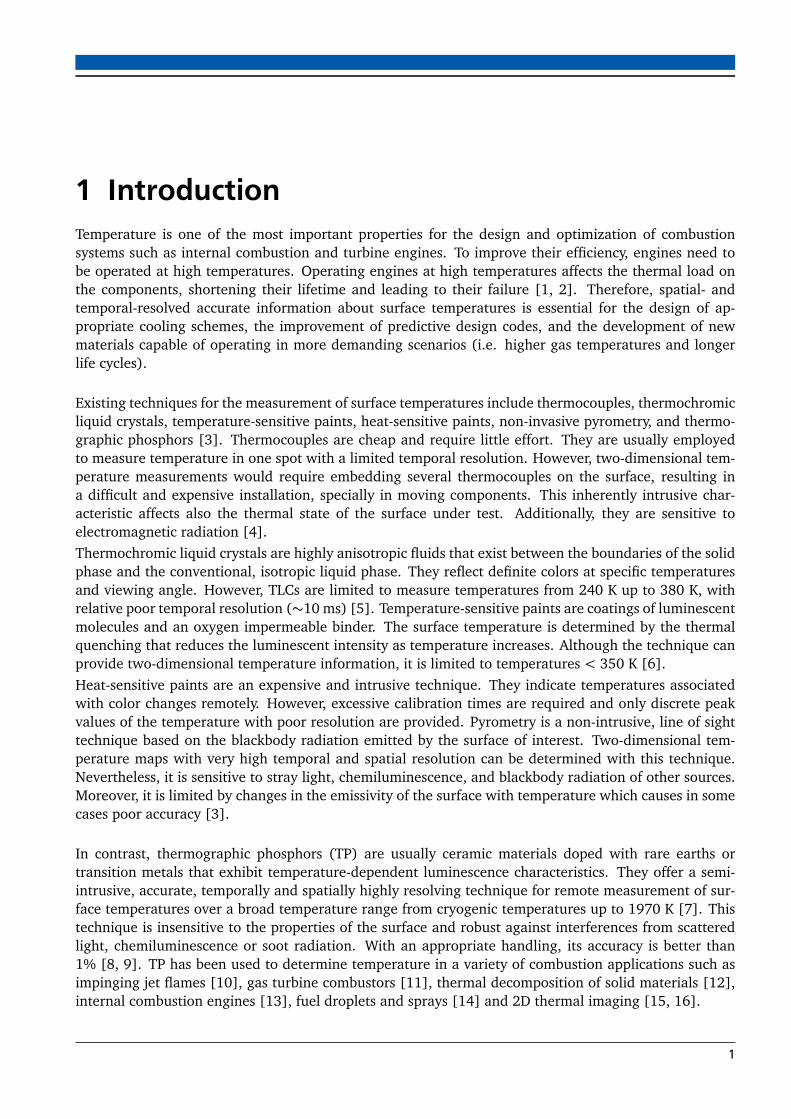
In general, luminescence processes involve the excitation of luminescent molecules, to jump to higherelectronic states, followed by different de-excitation phenomena. Vibration relaxation, internal conver-sion, intersystem crossing and emissions are example of de-excitation phenomena that return the excitedstate back to the ground or to an intermediate state [7]. Figure 2.1 depicts a simplified energy level dia-gram showing the main luminescence processes. Excitation involves the absorption of sufficient energyto raise a molecule’s electron form the ground state S0 into the electronic state S1, which generally occursin order of femtoseconds. The molecule does not remain excited continually as the amount of energyabsorbed must be released according to the principle of energy conservation. DIfferent de-excitationprocesses are of relevance in luminescence [7]:
• Fluorescence: a radiative transition from the excited state accomplished by the emission of a pho-ton. The emission wavelength is found to be less than the excitation wavelength due to energylevel differences, resulting in emissions of longer wavelengths. Fluorescence typically occurs in atimescale of less than 10−8 s.
• Intersystem crossing: a transition from the excited state S1 to the intermediate state T1. Intersystemtransitions require changes in electron spin and generally have an extremely low probability ofoccurrence. However, molecules containing heavy atoms (e.g. transition metals) often facilitateintersystem crossing, making these as common as internal conversions, in times from 10−10 to 10−8
s.
• Phosphorescence: if after an intersystem transition the molecule has not returned to its groundstate, phosphorescence is the transition from T1 to S0. The energy level of T1 is lower than that ofS1 and therefore the emission wavelength of phosphorescence is higher than that of fluorescence.Additionally, this process is orders of magnitude slower than fluorescence (> 10−8 s).
2.1.2 Thermographic phosphors
Phosphors are materials that non-thermally convert energy into electromagnetic radiation. They areusually defined as rare-earth or transition-metal-doped ceramic materials that emit visible light after ex-citation by short-wavelength light, X-ray radiation or electron bombardment [29]. Phosphors consist oftwo components: a host compound and an activator or doping agent from which the light is emitted. In
4
Fluorescence Phosphorescence
Intersystem Crossing
S1
T1
S0
Vibrational state
Electronic state
Figure 2.1: Simplified energy level diagram of the main luminescence processes.
the case of praseodymium-doped calcium titanate, CaTiO3:Pr3+ and chromium-doped gadolinium gal-lium oxide, Gd3Ga5O12:Cr3+, CaTiO3 and Gd3Ga5O12 are termed as host, the Pr3+ and Cr3+ ions asactivators or doping agents.
The excitation energy can be absorbed by the activator, by the host crystal or by another dopant (co-dopant). For the subsequent return from the excited state to the ground state, basically radiative trans-fer processes compete with non-radiative processes. Whereas the spontaneous emission of at least onephoton is involved in the first case, non-radiative processes only rely on internal energy transfer. Ther-mographic phosphors are those whose rates of the non-radiative processes are a function of temperaturedue to internal energy transfer processes that are enhanced by the temperature [29].
Because the doping agents are in a not-static host, temperature might have a significant effect on theluminescence behavior of the phosphor. As represented in the configurational coordinate diagram in Fig-ure 2.2, after excitation, electrons occupying an upper vibrational level of an excited state (point B) relaxto the ground vibrational level of that state (C) losing energy by releasing phonons. Following radiativeemission, the electrons reaching a higher vibrational level of the ground state (D) further lose energy(phonons) on their return to their ground state equilibrium (A) [7]. If the temperature is high enough,electrons in the excited state can intersect the ground state curve (point E) allowing vibrational relax-ation via phonon release to the ground state without any radiative emission. This can be described asthe absorption of thermal energy (phonon) from point C, which excites the electrons to the intersectionpoint E. Because non-radiative processes can now also take place, the observed luminescence intensityfrom a large quantity of excited ions decreases, explaining the thermal quenching behavior that changesthe luminescence properties of thermographic phosphors [7].
In some host materials, the outer crystal field, could cause another energy potential (known as chargetransfer state) that can be added on to the existing configuration coordinate diagram (Figure 2.3). Ex-cited electrons can now return to the ground state via the charge transfer (CT) curve. If an excitedelectron reaches an excited state of E3, it would normally return to the ground state by radiative emis-sion. However, if the electrons are further excited by elevated temperatures, the electrons can intersectthe crossover point of the CT curve, enabling the transfer of electrons to a lower energy level of E2without any radiative emission. Likewise, electrons in the E2 or E1 states can transfer their energy tothe ground state in the same way [7]. Different hosts will have the CT curve in slightly different places,thus explaining the different behavior of a doping agent in different hosts [54].
5

Ground State
Excited State
Intersection Point
Vibrational levels
Ex
cita
tio
n
Em
ission
Equilibrium distance of ground state
A
D
B E
C
Activation or thermal energy
Energy
Configurational Coordinate
Equilibrium distance of the excited state
Figure 2.2: Configurational coordinate diagram [7].
&
'"
(
)
*
"
Figure 2.3: Configurational coordinate diagram with charge transfer state [7].
As Brübach et al. [29] pointed out, in thermographic phosphors the distinction between the phe-nomenon of fast spin-allowed (fluorescence) and slow spin-forbidden transitions (phosphorescence) isnot well-defined, in this study the terminology is restricted to the general term, luminescence.
2.1.3 Praseodymium-doped Calcium Titanate, CaTiO3:Pr3+
In the thermographic phosphor praseodymium-doped calcium titanate, CaTiO3:Pr3+, the perovskiteCaTiO3 acts as host material and the Pr3+ ion as doping agent. In Figure 2.4, at room temperature,the structure of CaTiO3 is orthorhombic and is made up of corner-shared TiO6 octahedra with Ca ions inthe large cavities at the corners of the unit cell [59]. The Pr3+ ion has the [Xe] 4f2 configuration. Theenergy level scheme of Pr3+ up to about 25000cm−1, in Figure 2.5 (a), consists of a large number ofenergy levels. Upon excitation with UV or visible light, the emission spectrum can either be dominated
6

by emission from the 3P0 level (greenish-blue emission) or from the 1D2 level (red emission).
In CaTiO3:Pr3+, the Pr3+ ions are expected to occupy the C1h calcium sites of the CaTiO3. Upon UVexcitation, this phosphor shows only emission from the 1D2 level, which is located in the red spectralregion [59]. This attribution suggests the total quenching of the luminescence transition 3P0→ 3H4 tran-sition. Various non-radiative de-excitation pathways could explain the quenching of 3P0 luminescence inCaTiO3: (1) multi-phonon relaxation, (2) cross-relaxation within pairs of Pr3+ ions and (3) intersystemcrossing through either low-lying 4f15d1 levels or through Pr- to-metal charge transfer state (CTS) [60].
Figure 2.4: Perovskite structure of CaTiO3.
(b)(a)
Figure 2.5: (a) Energy level scheme of the Pr3+ ion up to about 25000cm−1, (b) Coordinate energy dia-gram for Pr3+ in CaTiO3 [60].
7

Boutinaud et al. [60] recently proposed that the presence of two very short Pr3+ - Ti4+ interatomicdistances of 3.17 Å in CaTiO3:Pr3+ makes possible a photon assisted energy transfer from Pr3+ toTi4+ at relatively low energy. This energy transfer, referred to as Pr3+ / Ti4+ Pr4+ / Ti3+ chargetransfer state (CTS), interferes strongly with the excited dynamics of the Pr3+ in CaTiO3:Pr3+, causingthe quenching of the otherwise prominent greenish-blue emission from the 3P0 level, as represented inFigure 2.5 (b).
2.1.4 Chromium-doped Gadolinium Gallium Oxide, Gd3Ga5O12:Cr3+
Chromium-doped gadolinium gallium oxide is a thermographic phosphor in which Gd3Ga5O12 serves ashost material for the luminescent transition-metal ions of Cr3+. Gd3Ga5O12 belongs to the cubic crys-talline system, has a garnet structure, with Ia3d space group and a bulk cell parameter (a0) of 12.376Å. This is why Gd3Ga5O12 is sometimes referred as GGG. The garnet structure is composed of a 24(c)dodecahedral site (D2 point symmetry) for Gd3+ with coordination number 8 and two sites for Ga3+, a16(a) octahedral site with a coordination number 6, and a 24(d) tetrahedral site of coordination number4. O2− ions occupy the 96(h) sites with each one being a member of two dodecahedra, one octahedronand one tetrahedron [61]. The garnet structure can be viewed as interconnected dodecahedra, octahe-dra and tetrahedra with shared O atoms at the corners of the polyhedra, as in Figure 2.6.
Figure 2.6: Structure of the Gd3Ga5O12 garnet [61].
The Cr3+ ions are expected to enter into the Ga3+ sites of the GGG. Depending on the crystal-fieldstrength, the lowest Cr3+ emitting level can be the 4T2 or the 2E states. Each excited state exhibitsdifferent luminescence properties due to the different electron-lattice coupling. As depicted in Figure2.7, at room temperature and atmospheric pressure, the Cr3+ in GGG emission is dominated by thespin-allowed 4T2 → 4A2 transition which results in a fast decay and a broad emission band. However,the narrow R-lines emission associated with the spin-forbidden transition from the 2E level to the 4A2ground state is expected to be also present [62].
8

Figure 2.7: Coordinate energy diagram for Cr3+ in Gd3Ga5O12 [62].
2.2 Temperature measurement with thermographic phosphors
2.2.1 Typical phosphor thermometry system
A typical phosphor thermometry system is illustrated in Figure 2.8. In general, an excitation source,usually a laser, is used to excite the phosphor that is bonded onto the surface of interest. The subsequentemission is passed through an optical filter to remove unwanted emissions at different wavelengths. Thelight is collected and converted into a signal using a detector. The stored data is analysed and comparedwith calibration data to determine temperature.
Detector
Laser Excitation
SurfaceEmission
Data
Adquisition
Filter
Surface
Thermographic
phosphor
Data
AnalysisCalibration
Data
Emission
Figure 2.8: Schematic of a typical phosphor thermometry system.
9

Thermographic phosphors offer surface thermometry with high spatial and temporal resolution overa broad temperature range, up to 1970 K. The method is rather insensitive to the properties of thesurface and robust against interferences from scattered light, chemiluminescence or soot radiation. Pro-vided careful handling, its accuracy is better than 1% [29]. Among the disadvantages of the phosphorthermometry systems are: decreasing signals with increasing temperatures, bonding of the phosphor,phosphor coating can be semi-intrusive or intrusive depending on thermal properties and thickness [7].
2.2.2 Temperature measurement strategies
Due to the complex phenomena involved in luminescence, appropriate calibration of the emission signalat well-known temperatures is required to relate luminescence properties and temperature. Figure 2.9summarized the classification of the temperature measurement strategies proposed by Brübach et al.[29]. The strategies can be classified according to the different response signals of the luminescencecharacteristics. The time-resolved luminescence characteristics become evident in the time-domain, i.e.in the decay of the luminescence after a pulsed excitation as well as in the frequency-domain, i.e. in thephase shift of the luminescence in reference to an amplitude modulated excitation.
Phosphor Thermometry
Time-resolved
Time domain
Frequency domain
Decay time
Rise time
Time-integrated
Single spectral band
(absolute intensity)
Two spectral bands
(intensity ratio)
Figure 2.9: Classification of temperature measurement strategies [29].
In the time domain, the transient luminescence intensity following a pulsed excitation can be approxi-mated by a mono-exponential decay characteristic. This decay process is faster at higher temperaturesdue to higher rates of non-radiative transitions. For this approach the temporal signal characteristic isreduced to the scalar value of the lifetime,τ, as a measure for temperature. For the less common rise-time approach, it is exploited that there are different potential energy transfers and paths that occur atdifferent timescales changing the rise time characteristics with temperature because of the properties ofthe crystal structure of the phosphor [7]. In the frequency domain, a continuous excitation wave is usedinstead of a pulsed one. The resulting wave will have a different amplitude and phase due to varioustime lags of certain luminescent processes. Consequently, the temperature sensitivity of this phase shiftis exploited for thermometry.
The time-integrated luminescence intensity of thermographic phosphors also depends on the tempera-ture. However, the determination of the absolute luminescence intensity is critical, as this depends onhardly reproducible boundary conditions like the excitation energy, the homogeneity of the phosphorlayer, the quality and stability of the alignment, impurities on the optics or other disturbing factors re-lated to the excitation source, the phosphor and the detector [29]. The use of the one spectral bandapproach demands an in-situ calibration, which is not feasible in many applications. Some drawbacks
10

are compensated by the normalization of one spectral band’s time-integrated luminescence intensity toanother one. Therefore, the method of the temperature-dependent intensity ratio reduces the signalintensity of two spectral bands to a scalar value by a simple quotient.
2.3 Sputtering
2.3.1 Interactions of ions with surfaces
Figure 2.10 represents the phenomena that may occur when an ion approaches the surface of a solid(also know as target): (1) The ion may be reflected, probably being neutralized in the process; (2) theimpact of the ion may cause the surface to eject an electron, usually referred to as a secondary elec-tron; (3) the ion may become implanted; (4) the ion impact may also be responsible for some structuralchanges such as vacancies, interstitials, and changes of stoichiometry or charge level; (5) the ion impactmay set up a series of collisions between atoms of the target, possibly leading to the ejection of one ofthese atoms [63]. This last interaction is know as sputtering.
In the sputtering process the bombarding ions strike the atomic array of the target, scattering the targetatoms in all directions, including some out of the target surface. Ions are usually used to bombard thetarget because they can be easily accelerated by an electric field. After the ion impact, the collisionphenomena in the target could result in the sputter ejection of an atom from the surface or gradualdissipation of the impact energy to lattice vibrations (i.e. heat). The sputter ejection is inefficient, withtypically 1% of the incident energy reappearing as the energy of the sputtered atoms [63].
(1) Reflected ions & neutrals
(2) Secondary electrons
(5) Sputtered atoms
Incident ion
May terminate within the target
Result in the ejection of a target atom
(sputtering)
orCollision sequence:
(3) Bombarding ions may be implanted
(4) Structural changes possible
Surface
Figure 2.10: Possible interactions of ions with surfaces (adapted from [63]).
11

2.3.2 Sputtering deposition
One of the applications of sputtering is the deposition of coatings on a surface. An ejected atom can,under certain circumstances, move through certain distance until it strikes and condenses on the surfaceof a receiver, which is known as a substrate. By repeating the process over and over, a coating of severalatomic or molecular layers of target material builds up on the substrate. The coating, between 100 nmand 3 µm, is called thin film. Sputtering deposition is a very versatile process that allows depositing alarge variety of materials, producing films with high purity, homogeneity and adhesion [40, 63].
(a) Single atom arrives
Substrate
(b) Migration Re-evaporation (c) Collision & Combination of single atoms
(d) Nucleation
“Islands” of atoms
Islands Islands
(e) Growth
Cross-section
(f) Island shape (g) Coalescence (h) Continuity
growing
Substrate
Figure 2.11: Formation of a thin film (adapted from [63]).
Sputtering deposition is carried out under vacuum. The material arrives at the substrate mostly in anatomic form. The atom diffuses around the substrate with a motion determined by its binding energy tothe substrate and is influenced by the nature as well as the temperature of the substrate. Energetically,the surface of the substrate has adsorption sites for the depositing and diffusing atom. As represented inFigure 2.11, once finding an adsorption site, the atom can jump into an adjacent site, might re-evaporateor join another diffusing single atom to form a doublet, which is less mobile but more stable than a singleatom. The chances of forming the atomic pair depend on the single atom density and on the arrival ordeposition rate. As time advances, other single atoms join he doublets to form triplets, quadrupletsand so on. This is known as the nucleation stage of the thin film growth, leading to the formationof quasi-stable "islands" with densities around 1010/cm2 [63]. The islands grow in size rather than innumber. Eventually they grow to be large enough to touch and agglomerate during the coalescencestage. Coalescence proceeds until the film reaches continuity, which usually occurs after the film isseveral Ångstroms in average thickness. During the island stage, each island is usually a single crystal orcontains just a few crystals. Therefore, on a polycrystalline substrate (e.g. stainless steel) the orientationof each island is random, so that the resulting film is either polycrystalline or amorphous.
2.3.3 Conventional sputtering system
Figure 2.12 depicts the schematic of a conventional direct current (DC) sputtering system. The materialto be sputtered is transformed into a sputtering target (nearly always a solid) which becomes the cathodeof an electrical circuit, and has a high negative voltage (DC) applied to it. The substrate, that is intendedto coat, is placed on an electrically grounded anode at a certain distance from the target. These electrodes
12

are housed in a chamber which is evacuated (known as base pressure). A sputtering gas, usually argon,is introduced into the chamber to some specified pressure (known as working pressure), commonlybetween 4 × 10⁻² and 16 × 10−2 mbar . The action of the electric field is to accelerate electronswhich in turn collide with argon atoms, breaking some of them up into argon ions and more electronsto produce the plasma. The charged particles are accelerated by the field, the electrons tending towardsthe anode (causing more ionization on the way) and the ions towards the cathode. When the ionsstrike the cathode, they undergo the possible interactions mentioned above. The secondary electrons areresponsible for maintaining the electron supply and sustaining the plasma. The sputtered atoms fromthe target fly off in random directions and some of them land on the substrate (anode), condense andform the thin film. The rate of film formation (deposition rate) on the substrate depends mainly on thesystem pressure, the nature of the sputtering gas and the power applied to the circuit.
Substrate
Target
Argon
Vacuum chamber
Target
DC power supply
+_
Figure 2.12: Schematic of a conventional DC sputtering system.
2.3.4 RF sputtering
If a substrate is intended to be coated with an electrically insulating material, DC sputtering is notsuitable. When an insulator-covered electrode (i.e. a target of an insulator material) is placed in anindependently sustained DC plasma, the surface of this electrode will charge up to a floating potential, sothat the fluxes of ions and electrons to the surface become equal, regardless of the potential applied to theelectrode, backing the insulator and generating the recombination of the ions and electrons at the surfaceof the electrode. To overcome this, an alternating voltage power, supplied at radio frequencies (RFs)around 10 MHz, can be used to generate the plasma. In this case, the target is alternately bombarded byions and then electrons so as to avoid charge build-up. The positive charge accumulated during one half-cycle can be neutralized by electron bombardment during the next half-cycle. The RF sputtering makesa more efficient use of the electron impact ionization, so that working pressures could be practicallyreduced down to 1 × 10⁻³ mbar [63].
13

2.3.5 Magnetron sputtering
Magnetron systems are used in sputtering to attempt to trap electrons near the target so as to increasetheir ionizing effect. This is achieved by using perpendicular electric and magnetic fields. An electronemitted in the normal direction from the target into a magnetic field B parallel to the surface of thetarget, as represented in Figure 2.13, is rapidly accelerated away from the target because there is astrong electric field in the space above the target’s surface. However, the electron stays within the spacenear the target in a cycloidal orbit due to the magnetic field. The net result is that the electron istrapped near the target. If trapped electrons do not collide, the loss process of fast electrons going to thesubstrate and walls of the vacuum chamber is eliminated. If the electron makes collisions (ionizing), thesustainability of the plasma is enhanced. Typical types of magnetrons include cylindrical, circular andplanar magnetrons, depending on the application [63].
e-
Electric fieldMagnetic field
Target
Figure 2.13: Motion of a electron ejected from the surface of the target into the region of a magneticfield parallel to the surface in the presence of a electric field.
14

3 Objectives
3.1 Main Objective
To evaluate the performance of sputtering as a technique to generate functional and stable coatings ofdifferent thermographic phosphors for applications of surface temperature measurements within com-bustion environments.
3.2 Specific objectives
• To prepare stable targets as sputter sources using sintering.
• To analyze the phase composition of the target materials via XRD.
• To determine appropriate parameters for sputtering the thermographic phosphors on stainless steelsubstrates.
• To physically and chemically characterize the sputtered coatings using surface science techniques.
• To verify the functionality at different temperatures of the thermographic phosphor coatings aftersputtering using laser techniques.
15

4 Materials and MethodsThis chapter details the methodology followed to prepare the phosphor targets and their characteriza-tion, the deposition of the thin films by RF magnetron sputtering, the chemical and physical charac-terization of the phosphor thin films and the evaluation of the temperature-dependent luminescenceproperties. At the end of the chapter, the description of the additional experiments on GGG:Cr powdersamples is also included.
4.1 Synthesis of the targets
4.1.1 CaTiO3:Pr3+ target
The CaTiO3:Pr3+ target was prepared by the sol-gel combustion method combined with high tempera-ture sintering. The sol-gel combustion method was used to prepare the precursor powder of CaTiO3:Pr3+
following two steps: xerogel formation and combustion reaction. The polymeric gel, combined withthe fast combustion reaction, makes the method suitable to synthesise multicomponent systems, likeCaTiO3:Pr3+, where the stoichiometry must be strictly maintained. After these steps the powder wasground and compressed to form the target. Finally, the target was sintered at 1373 K.
The flowchart in Figure 4.1 shows the experimental procedure followed to prepare the CaTiO3:Pr3+
precursor powders with a Pr doping concentration of 1 mol% (with respect to the Ca content). CaCO3,Ti(OC4H9)4, and Pr(NO3)3·5H2O were used as starting materials. During the first step, CaCO3 andTi(OC4H9)4 were converted into Ca(NO3)2 and Ti(NO3)4 in aqueous solution using nitric acid, HNO3.After this, Pr(NO3)3·5H2O was added to the solution. The metal nitrates aqueous solution was thenheated under magnetic stirring in the presence of citric acid (C6H8O7·H2O ), which acts as chelatingagent promoting gel polymerization. Next, the xerogel synthesis was performed at low temperature(353 K) during several hours to ensure the homogeneity at the atomic scale, preventing preferentialprecursor precipitations. The combustion reaction step is a strong exothermic and autocatalytic reactionof the xerogel. It was activated in an electric furnace at a temperature of 473 K during 20 minutes,resulting in a yellowish foam. The fastness of the combustion reaction prevented any phase segregationphenomena, preserving the stoichiometry. The foam was finally ground to form the precursor powder.The sol-gel combustion procedure was repeated for three different batches to produce enough precursorpowder for the target preparation. Table 4.1 summarizes the amounts of starting materials used for eachindividual batch.
Table 4.1: Amounts of starting materials used for the production of CaTiO3:Pr3+ precursor powders.
ComponentAmount (g)
Batch A Batch B Batch CPr(NO3)3·5H2O 0.0806 0.0757 0.0814
Ti(OC4H9)4 6.3040 5.9209 6.3640CaCO3 1.8579 1.7413 1.8716
C6H8O7·H2O 7.7851 7.3119 7.8592
The sintering of the target was divided in three steps: (1) the three batches of precursor powders weresintered in air at 873 K for 6 hours using the controlled temperature ramp in Figure 4.2 (a) in an electric
16

Ti(OC4H9)4(l) CaCO3(s) 65% HNO3
Ca(NO3)2 + Ti(NO3)4
aqueous solution Pr(NO3)3·5H2O (s) C6H8O7·H2O (s)
Stirring and heating
XerogelXerogel
Combustion
Yellowish foam
Grinding
Precursor powder
Figure 4.1: Flowchart of the sol-gel combustion method used to prepare the precursor powder ofCaTiO3:Pr3+.
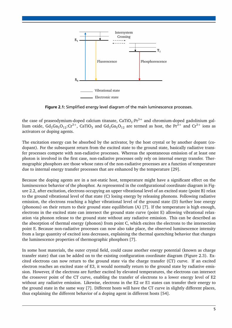
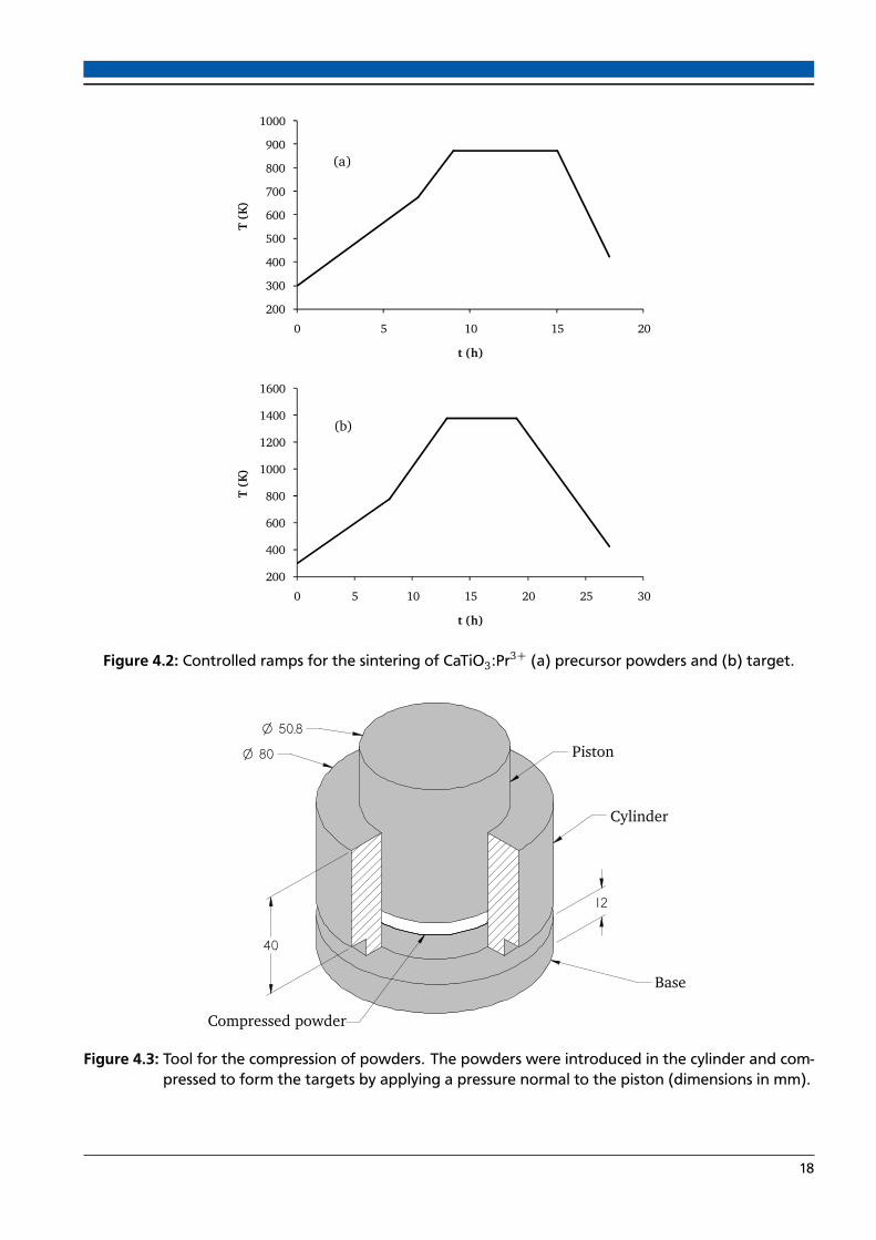
furnace (Carbolite CWF 1200, Tma x = 1473 K) equipped with a temperature controller (Eurotherm2416); (2) The three sintered batches were ground again, mixed and slowly compressed, using the tooldescribed in Figure 4.3, up to 980 MPa to form the target; (3) The target was finally sintered in airat 1373 K for 6 hours using the controlled temperature ramp in Figure 4.2 (b). The temperature forsintering the precursor powders was selected to guarantee the synthesis of CaTiO3:Pr3+ while keeping agood compressibility of the powder. The maximum temperature for sintering the target was limited bythe maximum temperature of the furnace.
4.1.2 Gd3Ga5O12:Cr3+ target
The Gd3Ga5O12:Cr3+ target, with a Cr doping concentration of 0.5 mol% (with respect to the total con-tent of metals), was prepared by high-temperature solid-state reactions using an ammonium hydroxideprocess as represented in Figure 4.4. Five individual batches, with the same composition, were pre-pared with the amounts listed in Table 4.2. For each individual batch, high-purity (99.99%) oxides ofgallium (Ga) and gadolinium (Gd) in the correct proportions were dissolved in hot, concentrated nitricacid (HNO3) under magnetic stirring. The stoichiometric amount of Cr(NO3)3·9H2O was added to thesolution. After stirring well, the Gd and Cr metal nitrates are in aqueous solution while the Ga2O3 staysas solid particles. A NH4OH solution was added to form a ultrafine precipitate of Gd(OH)3 and Cr(OH)3covering the Ga2O3 particles. This with the aim of increasing the contact area between the metal oxidesduring the solid-state reactions. The precipitate was then washed with water and dried in air to removethe NH4NO3 by-product and excess of NH4OH.
Table 4.2: Amounts of starting materials to produce the Gd3Ga5O12:Cr3+ target.Component Amount (g)
Cr(NO3)3·9H2O 0.0400Gd2O3 2.1750Ga2O3 1.8650
17
200
300
400
500
600
700
800
900
1000
0 5 10 15 20
T (
K)
t (h)
(a)
200
400
600
800
1000
1200
1400
1600
0 5 10 15 20 25 30
T (
K)
t (h)
(b)
Figure 4.2: Controlled ramps for the sintering of CaTiO3:Pr3+ (a) precursor powders and (b) target.
Figure 4.3: Tool for the compression of powders. The powders were introduced in the cylinder and com-pressed to form the targets by applying a pressure normal to the piston (dimensions in mm).
18

Ga2O3 (s) Gd2O3 (s) HNO3·H2O
Gd(NO3)3 (aq) + Ga2O3 (s) Cr(NO3)3·9H2O (s)
NH4OH
Stirring and heating
Washing and drying
Precipitate
Gd(OH)3 + Cr(OH)3
+ Ga2O3 (s)
Figure 4.4: Flowchart of the method used to prepare the GGG:Cr3+ target.
After drying, the precipitate was grounded. The five grounded powders were mixed and slowly com-pressed, with the tool in Figure 4.3, up to 980 MPa to form the target. The target was sintered in airat 1373 K for 6 hours, using the controlled ramp shown in Figure 4.5, to convert the hydroxide into acrystalline garnet of Gd3Ga5O12:Cr3+
800
1000
1200
1400
1600
T (
K)
200
400
600
0 10 20 30 40 50
t (h)
Figure 4.5: Controlled ramp for the sintering of the Gd3Ga5O12:Cr3+ target.
4.2 Characterization of the targets
The composition and crystal structure of the targets and the corresponding precursor powders was stud-ied using a X-ray diffraction technique (XRD). X-ray scattering is a family of non-destructive analyticaltechniques which provides information about the crystallographic structure and chemical composition ofsolids. These techniques are based on the scattering X-rays hitting a crystalline substance. X-ray wave-lengths are comparable with inter-atomic distances (∼1Å). Therefore, it is regarded an excellent meansof crystal diffraction study for this length scale. Atoms scatter X-ray waves, primarily through the atoms’
19

electrons that can emanate secondary spherical waves. This phenomenon is known as elastic scatter-ing, and the electron shell is known as the scatterer. A regular array of scatterers produces a regulararray of spherical waves. Although these waves cancel each other out for most of the directions throughdestructive interference, they add constructively in a few specific directions, determined by Bragg’s law:
n ·λ= 2 · d · sinθ (4.1)
where n is an integer determined by the order given, λ is the wavelength of the X-rays , d is the spacingbetween the planes in the atomic lattice and θ is the angle between the incident ray and the scatteringplanes.
Representative powder samples collected from the targets and the precursor powders were used for thecharacterization with X-ray diffraction. A powder sample consists of an enormous number of randomlyorientated small crystallites. In such a sample, various lattice planes are present in every possible ori-entation. For each set of planes, therefore, at least some crystals must be oriented at the Bragg angle,to the incident beam and thus, diffraction occurs for these crystals and planes. A powder diffractogramcontains information about the diffraction angles and their corresponding intensities. Factors such ascrystal class, lattice type, symmetry, unit cell parameter, the distribution and type of atoms in the unitcell affect the intensity and number of reflections. As a result, nearly all crystalline solids have a uniquepowder X-ray diffraction pattern in terms of position and intensities of the observed reflections.
The X-ray measurement of the powder samples was performed on a STOE Stadi P diffractometer atroom temperature. A position sensitive detector in Debye-Scherrer geometry was used (see Figure 4.6).In this geometry, a monochromatic incident beam uniformly illuminates the powder sample, the 2θangle between the incident and scattered beams, is fixed for a given Bragg reflection. The Debye-Scherrer geometry employs a parallel beam that uniformly illuminates the powder sample. The detectoris placed near the scattering plane. A series of slits, known as Soller slits, are employed to define theincident and scattered beam directions. The main advantage of this geometry is that the sample can beeasily rotated around its axis to obtain a good average and to eliminate part of the non-randomness ofthe powder sample.
Figure 4.6: Powder diffractometer in Debye-Scherrer geometry.
The diffractometer is equipped with a copper anode and curved germanium (111) monochromator withCu-Kα1 radiation of wavelength 1.54056 Å. The obtained powder X-ray pattern was analysed by usingthe software provided by STOE [64]. The materials were identified by comparing with well knownsubstances, with crystallographic data provided by the International Centre for Diffraction Data (ICDD)data base, which are included in the software [64].
20
4.3 Deposition of the thin films
4.3.1 Surface preparation machine
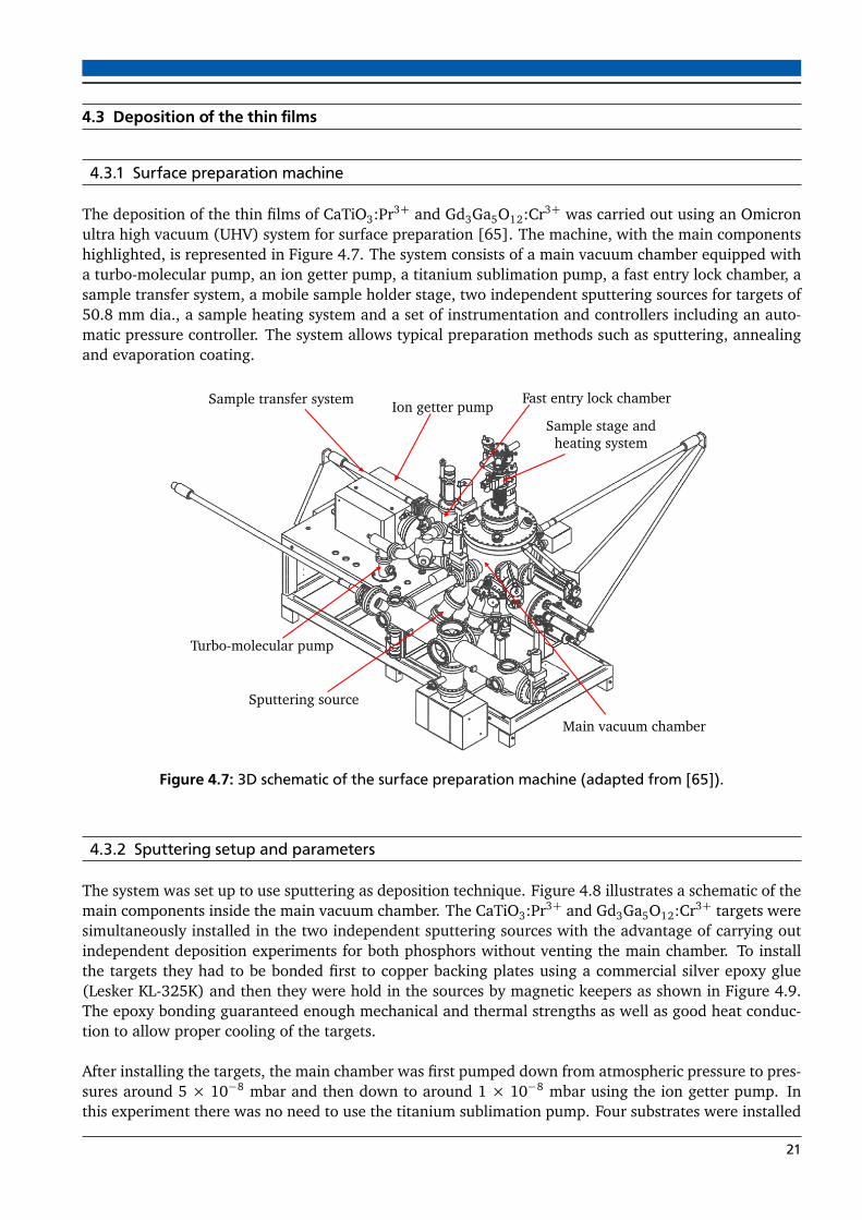
The deposition of the thin films of CaTiO3:Pr3+ and Gd3Ga5O12:Cr3+ was carried out using an Omicronultra high vacuum (UHV) system for surface preparation [65]. The machine, with the main componentshighlighted, is represented in Figure 4.7. The system consists of a main vacuum chamber equipped witha turbo-molecular pump, an ion getter pump, a titanium sublimation pump, a fast entry lock chamber, asample transfer system, a mobile sample holder stage, two independent sputtering sources for targets of50.8 mm dia., a sample heating system and a set of instrumentation and controllers including an auto-matic pressure controller. The system allows typical preparation methods such as sputtering, annealingand evaporation coating.
Figure 4.7: 3D schematic of the surface preparation machine (adapted from [65]).
4.3.2 Sputtering setup and parameters
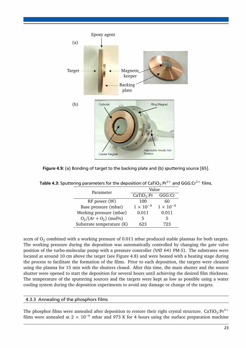
The system was set up to use sputtering as deposition technique. Figure 4.8 illustrates a schematic of themain components inside the main vacuum chamber. The CaTiO3:Pr3+ and Gd3Ga5O12:Cr3+ targets weresimultaneously installed in the two independent sputtering sources with the advantage of carrying outindependent deposition experiments for both phosphors without venting the main chamber. To installthe targets they had to be bonded first to copper backing plates using a commercial silver epoxy glue(Lesker KL-325K) and then they were hold in the sources by magnetic keepers as shown in Figure 4.9.The epoxy bonding guaranteed enough mechanical and thermal strengths as well as good heat conduc-tion to allow proper cooling of the targets.
After installing the targets, the main chamber was first pumped down from atmospheric pressure to pres-sures around 5 × 10⁻⁸ mbar and then down to around 1 × 10⁻⁸ mbar using the ion getter pump. Inthis experiment there was no need to use the titanium sublimation pump. Four substrates were installed
21

Rotating sample stage
Heater stage
Source shutter (opened)
Main shutter
Substrates holder
Substrates
Sputtering sources
Source shutter (closed)
GGG:Cr target
CaTiO3:Pr target
Figure 4.8: Details of the set up inside the main vacuum chamber.
simultaneously during each individual experiment using a 2-inch diameter sample holder. In the case ofCaTiO3:Pr3+, two substrates of stainless steel (1.4301 or 304) and two of indium tin oxide (ITO)/glasswere used while for GGG:Cr3+ three substrates of stainless steel and one of quartz glass were employed.For each deposition experiment the sample holder with new substrates could be easily installed insidethe main chamber using the fast entry lock and the transfer system without venting the whole system.
Films of CaTiO3:Pr3+ and GGG:Cr3+ were deposited by RF magnetron sputtering, using the same setup but with different parameters. Table 4.3 summarizes the most important parameters used for thedeposition of the CaTiO3:Pr3+ and GGG:Cr3+ films. As both targets are insulators typical DC sputteringconfigurations are not suitable. When an insulator is placed in a DC discharge, its surface charges up to afloating potential, so that the fluxes of ions and electrons to the surface become equal and recombine onthe surface of the target extinguishing the discharge. To overcome this, a RF discharge can be applied sothat the positive charge accumulated during one half-cycle can be neutralized by electron bombardmentduring the next half-cycle. A RF generator (Seren IPS Inc. R301, max. power 400 W) and an automaticmatching network (Seren IPS Inc. MC2) were used to produce an almost continuous discharge since thetarget is alternately bombarded by ions and then by electrons to avoid charge build-up. Additionally,a circular magnetron configuration (see Figure 4.9 (b)) was employed to trap electrons near the targetincreasing their ionizing effect. In this configuration the sputtered material has a pronounced forwarddirection perpendicular to the center magnet. Therefore, the sample holder was rotated to ensure gooduniformity of the film thickness.
High-purity Argon (grade 5.5) was selected as sputtering gas due to its facility to be ionized, inertnature and availability. A small amount of oxygen was added to the sputtering gas with two purposes,avoiding any change of the targets oxidation state and restoring the stoichiometry of deposited filmswhich usually have a deficiency of oxygen when using metal oxide targets. Flows of 38 sccm of Ar and 2
22
Epoxy agent
Target Magnetic keeper
Backing plate
(a)
(b)
Figure 4.9: (a) Bonding of target to the backing plate and (b) sputtering source [65].
Table 4.3: Sputtering parameters for the deposition of CaTiO3:Pr3+ and GGG:Cr3+ films.
ParameterValue
CaTiO3:Pr GGG:CrRF power (W) 100 60
Base pressure (mbar) 1 × 10⁻⁸ 1 × 10⁻⁸
Working pressure (mbar) 0.011 0.011O2/(Ar +O2) (mol%) 5 5
Substrate temperature (K) 623 723
sccm of O2 combined with a working pressure of 0.011 mbar produced stable plasmas for both targets.The working pressure during the deposition was automatically controlled by changing the gate valveposition of the turbo-molecular pump with a pressure controller (VAT 641 PM-5). The substrates werelocated at around 10 cm above the target (see Figure 4.8) and were heated with a heating stage duringthe process to facilitate the formation of the films. Prior to each deposition, the targets were cleanedusing the plasma for 15 min with the shutters closed. After this time, the main shutter and the sourceshutter were opened to start the deposition for several hours until achieving the desired film thickness.The temperature of the sputtering sources and the targets were kept as low as possible using a watercooling system during the deposition experiments to avoid any damage or change of the targets.
4.3.3 Annealing of the phosphors films
The phosphor films were annealed after deposition to restore their right crystal structure. CaTiO3:Pr3+
films were annealed at 2 × 10⁻⁶ mbar and 973 K for 4 hours using the surface preparation machine
23

described in section 4.3.1. Due to temperature limitations of the preparation machine, GGG:Cr3+ filmswere annealed at 1173 K for 12 hours in N2 atmosphere at atmospheric pressure and using an electricquartz tube furnace Carbolite (SPLF 77720, Tma x = 1673 K) with an automatic temperature controller(Eurotherm 2416).
4.4 Characterization of the thin films
4.4.1 X-ray photoelectron spectroscopy
X-ray photoelectron spectroscopy (XPS) was used to investigate the chemical composition of the de-posited films. As represented in Figure 4.10 (a), XPS is based on the fact that a photon of sufficientlyshort wavelength (i.e. high energy) can ionize an atom, producing an ejected free electron by the pho-toelectric effect. Surface analysis by XPS is accomplished by irradiating a sample with monochromaticx-rays and measuring the energy of the detected electrons. The X-rays have usually a limited penetration,of the order of 1 to 10 micrometers, in solids [66]. The kinetic energy KE of the emitted electrons (thephotoelectrons) depends on the energy of the photon hv and can be expressed by:
KE = hv − BE −φs (4.2)
where BE is the binding energy of the atomic orbital from which the electron originates and φs isthe spectrometer work function. The binding energy may be regarded as the energy difference be-tween the initial and final states after the photoelectron has left the atom. Because there is a variety ofpossible final states of the ions from each type of atom, there is a corresponding variety of kinetic ener-gies of the emitted electrons. Moreover, there is a different probability or cross-section for each final state.
Kinetic Energy
0 -
0 -
Fermi Level
Vacuum level
Photon hv Photoelectron
Auger electron
Binding Energy
1s
2s
2p3s
(a) (b)
Figure 4.10: (a) XPS emission process and (b) relaxation process for a model atom.
Figure 4.11 schematically represents the relative binding energies and ionization cross-section of an ex-ample atom of uranium. By definition, the Fermi level corresponds to zero binding energy and the depthunder the Fermi level in the figure indicates the binding energy of the electron or the relative energyof the ion remaining after electron emission. The line lengths indicate the relative probabilities of thevarious ionization processes. The p, d and f levels become split upon ionization, leading to vacancies
24

in the p1/2, p3/2, d3/2, d5/2, f5/2 and f7/2. Because each element has a unique set of binding energies,XPS can be used to identify and determine the concentration of the elements in the surface [66]. Augerelectrons may be emitted because of relaxation of the excited ions remaining after photoemission. Asrepresented in Figure 4.10 (b), an outer electron falls into the inner orbital vacancy, and a second elec-tron is simultaneously emitted, carrying off the excess of energy.
Bin
ding
Ene
rgy
[eV
]
Cross-section
Bin
ding
Ene
rgy
[eV
]
Figure 4.11: Relative binding energies and ionization cross-section of Uranium (adapted from [66]).
The ionization process in the sample occurs at a depth of a few micrometers but only those electrons thatoriginate within tens of angstroms below the surface can leave the surface without energy loss produc-ing the peaks in the spectra. The electrons that undergo inelastic loss processes before emerging formthe background. The electrons leaving the sample are detected by an electron spectrometer accordingto their kinetic energy. The analyzer is usually operated as an energy window, referred to as pass en-ergy, accepting only those electrons having an energy within this range. The pass energy is fixed andthe scanning for different energies is accomplished by applying a variable electrostatic field before theanalyzer. Photoelectrons are finally detected as discrete events recording the number of electrons for agiven detection time and energy.
The XPS system used for the analysis of the deposited films consisted of an Al-Kα source (operatingat 15kV and 400 W), a monochromator (Specs FOCUS 500), a hemispherical energy analyzer (SpecsPHOIBOS 150) with a lens aperture of 1.5 kV and a slit of 7 × 20 mm, and an electron multiplierdetector (Specs MCD-9). The measurements were performed at 1 × 10⁻¹⁰ mbar with an excitationenergy of 1486.61 eV and a pass energy of 20 eV. Survey scans were measured up to binding energiesof 1300 eV with steps of 0.5 eV. For quantification purposes, detailed scans of the main peaks weremeasured with steps of 0.05 eV. The spectra were recorded and analyzed using the SpecLab software.
25

4.4.2 XRD of the thin films
The conventional configuration used for X-ray diffraction (XRD) of thick samples is the Bragg-Brentanogeometry. In this one, the X- ray beam is incident at an angle typically between 15 and 50. The depthof penetration into the sample is given by the absorption length times the sine of the incidence angle.If the sample is a thin layer, most of the X-ray beam passes through the film and is scattered by thesubstrate. To study the crystal structure of the thin films and since polycrystalline substrates of stainlesssteel were used for the deposition, the thin-film XRD configuration shown in Figure 4.12 was chosen tomaximize the XRD signal from the thin film while suppressing the XRD signal from the substrate.
X-ray source
Detector
Monochromator Thin film
Soller slits
2.5°
Sample holderSubstrate
Figure 4.12: Stadi P diffractometer in the thin-film configuration.
The key in thin-film XRD is to choose very small angles of incidence, increasing the path length of theX-rays in the film and reducing the amount of X-rays that penetrate through to the substrate. An inci-dence angle of 2.5 was set using the same STOE Stadi P diffractometer. During the measurements theincidence angle was fixed and the detector scanned over the range of diffraction angles because most ofthe diffraction peaks from the samples lie in the region 20 ≤ 2θ ≤ 100.
4.4.3 Film thickness
Mean values of the film thickness were estimated using a surface profilometer (Bruker Dektak XT). Thisis an instrument commonly used for surface texture analysis as it measures the surface topography of asample to reveal a topographical image of the surface. The surface profilometer was equipped with adiamond-tipped stylus moving vertically and laterally to scan across the surface of the sample. To esti-mate the mean thickness of the deposited films, the stylus profilometer measured vertical displacementsas a function of position at different edges of the films. The film thickness was then calculated as themean value of the difference of the vertical displacement at the film position and the vertical displace-ment at the substrate position. For a better estimation, the films deposited on ITO/glass and quartzglass were used for the measurements of the CaTiO3:Pr3+ and GGG:Cr3+ films, respectively, due to theirsuperior surface quality over the stainless steel substrates.
For comparison, the thickness of the films were estimated using a thickness/deposition rate monitor(Sycon Instruments STM-100/MF) prior deposition. This instrument uses the time-proven 6 MHz oscil-lating quartz crystal as the sensor device. The sensor was located inside the main vacuum chamber at the
26

same position of the substrates. The plasma was ignited with the same parameters of Table 4.3, exceptfor the high temperatures of the substrates to avoid damaging the sensor. The thickness / deposition ratemonitor uses the resonant frequency of the exposed quartz crystal to sense the mass of deposited filmsattached to its surface. There is a known relationship between the mass of such a film and the measuredfrequency of the sensor crystal. Knowing the frequency change due to accumulated mass, film thicknessis determined by the following equation:
A f =
Nq · Dq
π · D f · Z · Fc
· arctan
Z · tan
π · (Fq − Fc)
Fq
(4.3)
where A f (Å) is the film thickness, Nq = 1.668 × 10¹³ HzÅ is the frequency constant for AT-cut quartz,Dq = 2.648 g/cm3 is the density of quartz, D f (g/cm3) is the density of the material, Fq and Fc are thefrequencies of the sensor crystal prior and after depositing material on it, respectively (these values arenot revealed by the manufacturer), and Z is a factor of the material defined as:
Z =
Dq · Uq
D f · U f
(4.4)
where Dq and D f are the densities and Uq and U f are the shear modulus of the quartz and film materials,respectively.
4.5 Evaluation of the thermographic functionality of the thin films
4.5.1 Measurement of the luminescence lifetime
To evaluate the luminescence functionality of CaTiO3:Pr3+ and GGG:Cr3+ thin films, measurements ofthe luminescence lifetime at different temperatures were carried out using the setup represented in Fig-ure 4.13. The fourth harmonic (266 nm) of a non-focused, pulsed, Q-switched Nd:YAG laser (QuantaRay, INDI, repetition rate: 10 Hz, pulse width 5-8 ns) was used to excite luminescence. The pulse energywas adjusted by the combination of a half-wave-plate and a Glan polarizer and it was referenced by apyroelectric energy detector (Gentech- EO, QE25-SP-S-MB). The laser beam profile was spatially limitedby two apertures with diameters of 4 mm and 2 mm placed at distances of 3000 and 1200 mm from thephosphor sample, respectively.
For spatial filtering and for minimizing the influence of blackbody radiation and other interfering light,the emitted luminescence light was imaged onto a pinhole (d = 100 µm) by a commercial 85 mm Nikkorcamera lens. In order to enable homogeneous illumination of the photomultiplier tube (PMT) the signalwas collimated by a plano-convex lens (f = 30 mm) behind the pinhole. The photomultiplier currentwas read out by an oscilloscope (Tektronix 5032B, 350 MHz) at an input resistance of 512 Ω and a cablecapacity of C = 300 pF resulting in a threshold lifetime of τ = 153 ns.
For measurements above room temperature, the samples were placed within an optically accessible tubefurnace (Carbolite, CTF 12/100/900, inner tube diameter: 105 mm, tube length: 900 mm, Tma x = 1473K). The furnace was equipped with a type N thermocouple (TMH GmbH, Maintal, Germany, specifiedaccuracy of 0.4% in the designated temperature range), which was directly mounted in contact with thephosphor sample. Prior to the measurement of temperature/luminescence characteristics, the furnacewas heated up until the sample reached its desired maximum temperature. After switching off the fur-nace, measurements of the lifetime decay were performed at decreasing temperature in steps of ∆T =10 K. Due to the inherent decelerating of the cooling down rate, the measurements were aborted before
27
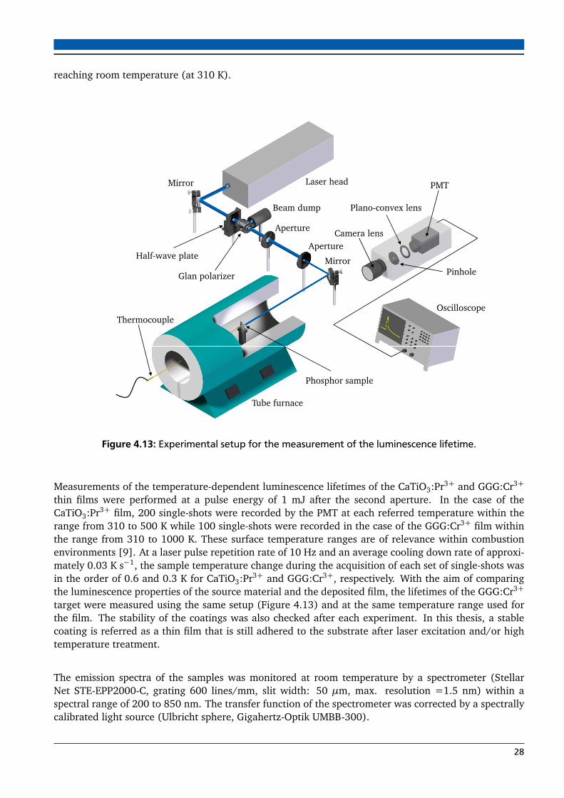
reaching room temperature (at 310 K).
Laser headMirror
Aperture
Aperture
Mirror
Beam dump
Half-wave plate
Camera lens
Pinhole
Plano-convex lens
PMT
Phosphor sample
Tube furnace
OscilloscopeThermocouple
Glan polarizer Pinhole
Figure 4.13: Experimental setup for the measurement of the luminescence lifetime.
Measurements of the temperature-dependent luminescence lifetimes of the CaTiO3:Pr3+ and GGG:Cr3+
thin films were performed at a pulse energy of 1 mJ after the second aperture. In the case of theCaTiO3:Pr3+ film, 200 single-shots were recorded by the PMT at each referred temperature within therange from 310 to 500 K while 100 single-shots were recorded in the case of the GGG:Cr3+ film withinthe range from 310 to 1000 K. These surface temperature ranges are of relevance within combustionenvironments [9]. At a laser pulse repetition rate of 10 Hz and an average cooling down rate of approxi-mately 0.03 K s−1, the sample temperature change during the acquisition of each set of single-shots wasin the order of 0.6 and 0.3 K for CaTiO3:Pr3+ and GGG:Cr3+, respectively. With the aim of comparingthe luminescence properties of the source material and the deposited film, the lifetimes of the GGG:Cr3+
target were measured using the same setup (Figure 4.13) and at the same temperature range used forthe film. The stability of the coatings was also checked after each experiment. In this thesis, a stablecoating is referred as a thin film that is still adhered to the substrate after laser excitation and/or hightemperature treatment.
The emission spectra of the samples was monitored at room temperature by a spectrometer (StellarNet STE-EPP2000-C, grating 600 lines/mm, slit width: 50 µm, max. resolution =1.5 nm) within aspectral range of 200 to 850 nm. The transfer function of the spectrometer was corrected by a spectrallycalibrated light source (Ulbricht sphere, Gigahertz-Optik UMBB-300).
28

4.5.2 Spatially resolved lifetime characteristics
To evaluate the spatial homogeneity of the lifetime characteristics of the deposited films, the experimen-tal setup was modified, as represented in Figure 4.14, to measure the 2D luminescence lifetime of thedeposited films. The Gaussian beam profile was converted into a top-hat profile by a beam homogenizer(Holo Or, Israel, diffusing angle: 0.68) in order to ensure spatially homogeneous excitation. The lumi-nescence was monitored by a high-speed CMOS camera (LaVision High Speed Star 6, maximum framerate: 675 kHz, dynamic range: 12 bit), equipped with a Nikkor 50 mm photo lens. Due to signal strengthlimitations, this experiment was only carried out for the GGG:Cr3+ thin film. The spatially resolved lu-minescence was evaluated at room temperature recording images of 100 single-shots with an excitationenergy of 40 mJ (after the first aperture).
CMOS cameraAperture
Camera lens
Laser beam
Beam homogenizer
Mirror
Thin film sample
Laptop computer
Figure 4.14: Modified experimental setup for the spatially resolved experiment.
4.5.3 Data evaluation
For the evaluation of the temperature-dependent luminescence characteristics, the measured decay sig-nals of the thin films were converted to scalar lifetimes, τ, using the iterative fitting algorithm of Brübachet al [8], modified by Fuhrmann et al [67]. In this algorithm, the single-shot waveforms are approxi-mated by a mono-exponential decay
I(t) = I0ex p−tτ + b (4.5)
where I0 is the initial intensity at t0 and b is the off-set intensity, which is computed by averaging thesignal intensity prior to the respective laser pulse. The linear regression of the sum (LRS), as introducedby Everest and Atkinson [68], is applied to determine the luminescence lifetime τ. LRS uses the fact thatthe integral of the decay waveform (Equation 4.6)
∫ t
o
I(t)d t =
∫ t
o
(I0ex p−tτ + b)d t = τ(I0+ b)−τI(t) + bt (4.6)
29

can be rewritten to have the decay waveform as a function of its own integral in a linear equation(Equation 4.7) and thus least- squares fitting can then be applied to determine the lifetime τ.
I(t) = I0+ b−1
τ
∫ t
o
I(t)d t +bt
τ(4.7)
When using phosphors like GGG:Cr3+ that are able to record temperatures over a broad temperaturerange, the lifetimes generally change over several orders of magnitude requiring the adaption of the de-tection system settings (i.e observation length ∆t, trigger point t0, etc.). Therefore, iteratively adaptedfitting windows are used to avoid inaccuracies on the determination of the lifetimes.
As represented in Figure 4.15, the algorithm is related to the lifetime τ instead of∆t. The fitting windowstarts at t1 = t0+ c1τ and ends at t2 = t0+ c2τ, where t0 is the instant of the laser trigger and c1 and c2are two constants. As τ is one of the unknown quantities, the fitting routine has to be applied iterativelyusing the initial guess τ0 = c0∆t, where c0 is a constant. For the iteration, the evaluated lifetime of thecurrent iteration step is used for the definition of the next step’s fitting window and for the new initialguess of the LRS algorithm. The convergence criterion is achieved when the difference of the maximumand the minimum τ of the last three steps is less than one thousandth of the average τ of these steps:
max(τi,τi−1,τi−2)−min(τi,τi−1,τi−2)< 10−3 ·
1
3(τi +τi−1+τi−2)
(4.8)
0122
0111
tct
tct
i
i
+=
+=
−
−
τ
τ
Linear regression of the
1−iτ
1−iτtc ∆=
00τ
Signal regression of the sum (LRS)
Convergence 1+= ii
Signal
iτ
iτ
resultiττ =
Figure 4.15: Flow chart of the algorithm using the iterative fitting window.
In the case of the the spatially resolved 2D luminescence evaluation, images acquired by the camera havebeen background subtracted and subsequently corrected for nonlinearity of the CMOS chip prior to theapplication of the iterative fitting algorithm for the temporal convolution of each pixel.
30

4.6 Additional experiments with GGG:Cr3+ powders
Experiments with GGG:Cr3+ powders varying the doping concentration of Cr3+ were performed to studythe temperature-dependent luminescence characteristics. This phosphor has a potential for thermo-graphic applications in combustion systems where temperature measurements with high spatially andtemporal resolutions are required. Additionally, the effect of co-doping with Cerium (Ce), as a way toreduce the afterglow and improve the luminescence characteristics of GGG:Cr3+, was also evaluated.
Five samples of GGG:Cr3+ with doping concentrations 0.125, 0.25, 0.5, 1, and 2 mol% of Cr (with respectto the total content of metals) and two samples of GGG:Cr,Ce (0.5 mol% Cr) co-doped with 0.038 and0.114 % by mass Ce, respectively, were prepared following the procedure described in Section 4.1.2 withsome variations. The amount of starting materials are summarized in Table 4.4. (NH4)2Ce(NO3)6 wasused as Ce source. After drying in air at 373 K, the samples were ground, sintered in air at 1373 K for 6hours, ball milled, sintered again in air at 1673 K for 3 hours, and ball milled again to improve the crystalstructure of the powders. The crystal structure of the samples was studied and compared by XRD (seeSection 4.2) while luminescence lifetimes were measured, using the setup described in Section 4.5.1, inthe range from 480 to 670 K and the data were analyzed according to Section 4.5.3.
Table 4.4: Amounts of starting materials to produce the GGG:Cr and GGG:Cr,Ce powders.Amounts (g)
Component GGG:Cr (mol%) GGG:Cr (0.5 mol%),Ce ( %w)0.125 0.25 0.5 1 2 0.038 0.114
Cr(NO3)3·9H2O 0.0080 0.0160 0.0320 0.0640 0.1281 0.0661 0.0661Gd2O3 1.0875 1.0875 1.0875 1.0875 1.0875 2.1749 2.1749Ga2O3 0.9372 0.9372 0.9372 0.9372 0.9372 1.8744 1.8744
(NH4)2Ce(NO3)6 0 0 0 0 0 0.0060 0.0180
31

5 Results and DiscussionThis chapter presents first the results on the preparation process of the CaTiO3:Pr3+ and GGG:Cr3+ tar-gets. Next, the evaluation of the sputtering deposition of phosphor thin films is presented along withthe analysis of the chemical composition and crystal structure of the thin films. Then, the luminescencecharacteristics of the deposited thin films of CaTiO3:Pr3+ and GGG:Cr3+ are evaluated at different tem-peratures. Additionally, an evaluation of spatially resolved lifetime characteristics of the GGG:Cr3+ ispresented and discussed. Finally, the chapter includes the results of the effect of doping concentrationon the temperature-dependent characteristics of GGG:Cr3+ powders with and without co-doping withcerium.
5.1 Phosphor targets
The target is one of the most important component of a sputtering system since it is the source materialfor the film deposition. A stable sputtering target contains the components and stoichiometry desired inthe film and it should have the following characteristics: (1) mechanical strength, (2) thermal strength,and (3) proper dimensions to fit in the sputtering sources. The CaTiO3:Pr3+ and GGG:Cr3+ targets wereprepared in the lab following the procedure detailed in section 4.1.
5.1.1 CaTiO3:Pr3+ target
A stable CaTiO3:Pr3+ target with a Pr doping concentration of 1 mol% (with respect to the Ca content)was prepared. The precursor powder was synthesised in three different batches, namely, A, B and C,to produce enough amount of material for the target. The amounts of starting materials for each batchvaried slightly since the Ti(OC4H9)4 was in liquid state, it was added first to the solution, and due tothe preparation method the final amount added varied slightly. The amounts of the other starting ma-terials were recalculated to keep the right stoichiometry. XRD measurements of the powders sintered at873 K for 6 hours were carried out to verify that the three different batches had the same crystal structure.
Fig 5.1 presents the XRD patterns of powders samples from the three batches. As can be observed, at thistemperature the powder of the three batches developed the same crystal structure. The main diffractionpeaks (1 2 1), (0 4 0), (0 4 2), (2 4 2), and (1 6 1) of the orthorhombic CaTiO3 standard powderdiffraction file ICSD 16688 [69] can be identified in the patterns. Moreover, the intensity ratios of themain peaks are basically equal. The small differences on the relative intensities can be attributed todifferences on the amounts of powder sample used for each measurement. The shape of the backgroundcorresponds to the amorphous structure of the adhesive tape employed to hold the powder samples.Background subtraction was not performed since XRD was not used in the present study for quantitativecalculations.
Once verified the reproducibility of the preparation method, a total of 6.5 g of sintered precursor powderwas compressed at 980 MPa, resulting in a target of 50.8 mm of diameter and 4 mm thickness with highflatness. At this step, the use of less than 6 g of powder produced targets with low mechanical strengthwhile targets made from more than 7 g were not compressed enough, showing some cracks at the crosssection, due to limitations on the maximum pressure applied (980 MPa). The target was sintered in airat 1373 K for 6 hours. The flatness of the target was maintained during this step by two flat ceramic
32

plates, one on the top and one on the bottom of the target. After sintering the target shrank, resulting inthe stable target of 45 mm of diameter and 3 mm of thickness shown in Figure 5.2.
0
20
40
60
80
100R
elat
ive
Inte
nsit
y (a
.u.)
Batch A
Batch B
Batch C
20 30 40 50 60 70 80 900
50
100
2 θ
ICSD 16688(1 2 1) (0 4 0)
(2 4 2)(1 6 1)(0 4 2)
Figure 5.1: XRD patterns of the three different batches of CaTiO3:Pr3+ precursor powder along with thestandard powder diffraction file ICSD 16688 [69].
Figure 5.2: CaTiO3:Pr3+ target (diameter 45 mm).
The composition and crystal structure of the CaTiO3:Pr3+ target was studied using XRD. The powdersample was collected by scratching the surface of the target. Figure 5.3 shows the XRD pattern of thetarget’s sample. All the reflections of the orthorhombic CaTiO3 from 2θ = 20 to 90 are present. Themain peaks (1 2 1) and (0 4 0) are sharp and well-developed. The XRD result indicates that the target issingle phase CaTiO3:Pr3+ with high crystallinity.
33
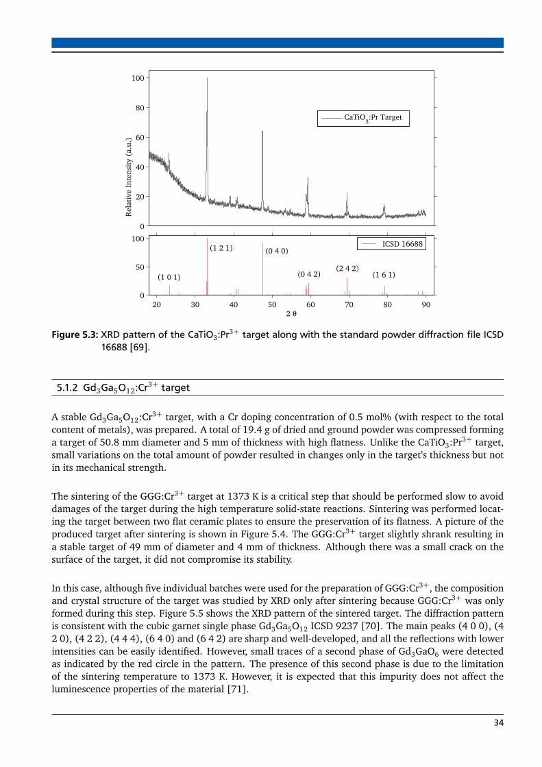
0
20
40
60
80
100
Rel
ativ
e In
tens
ity
(a.u
.)CaTiO
3:Pr Target
20 30 40 50 60 70 80 900
50
100
2 θ
ICSD 16688
(1 0 1)
(1 2 1) (0 4 0)
(0 4 2)(2 4 2)
(1 6 1)
Figure 5.3: XRD pattern of the CaTiO3:Pr3+ target along with the standard powder diffraction file ICSD16688 [69].
5.1.2 Gd3Ga5O12:Cr3+ target
A stable Gd3Ga5O12:Cr3+ target, with a Cr doping concentration of 0.5 mol% (with respect to the totalcontent of metals), was prepared. A total of 19.4 g of dried and ground powder was compressed forminga target of 50.8 mm diameter and 5 mm of thickness with high flatness. Unlike the CaTiO3:Pr3+ target,small variations on the total amount of powder resulted in changes only in the target’s thickness but notin its mechanical strength.
The sintering of the GGG:Cr3+ target at 1373 K is a critical step that should be performed slow to avoiddamages of the target during the high temperature solid-state reactions. Sintering was performed locat-ing the target between two flat ceramic plates to ensure the preservation of its flatness. A picture of theproduced target after sintering is shown in Figure 5.4. The GGG:Cr3+ target slightly shrank resulting ina stable target of 49 mm of diameter and 4 mm of thickness. Although there was a small crack on thesurface of the target, it did not compromise its stability.
In this case, although five individual batches were used for the preparation of GGG:Cr3+, the compositionand crystal structure of the target was studied by XRD only after sintering because GGG:Cr3+ was onlyformed during this step. Figure 5.5 shows the XRD pattern of the sintered target. The diffraction patternis consistent with the cubic garnet single phase Gd3Ga5O12 ICSD 9237 [70]. The main peaks (4 0 0), (42 0), (4 2 2), (4 4 4), (6 4 0) and (6 4 2) are sharp and well-developed, and all the reflections with lowerintensities can be easily identified. However, small traces of a second phase of Gd3GaO6 were detectedas indicated by the red circle in the pattern. The presence of this second phase is due to the limitationof the sintering temperature to 1373 K. However, it is expected that this impurity does not affect theluminescence properties of the material [71].
34

Figure 5.4: Gd3Ga5O12:Cr3+ target (diameter 49 mm).
0
20
40
60
80
100
Rel
ativ
e In
tens
ity
(a.u
.)
GGG:Cr Target
10 20 30 40 50 60 70 80 900
50
100
2 θ
ICSD 9237
(3 2 1)(2 1 1)
(4 0 0)
(4 2 0)
(4 2 2)
(5 2 1) (6 1 1) (4 4 4)(6 4 2)
(8 0 0)
(6 4 0)
(8 4 0)(8 4 2)
(6 4 4) (8 8 0)
(10 4 0)
Figure 5.5: XRD pattern of the Gd3Ga5O12:Cr3+ target along with the standard powder diffraction fileICSD 9237 [70].
5.2 Thin films of thermographic phosphors
Thin films of CaTiO3:Pr3+ and GGG:Cr3+ were deposited by RF magnetron sputtering using the parame-ters of Table 4.3. The deposition was attempted first using only Argon as sputtering gas. However, afterseveral hours of sputtering, both targets revealed a dark layer. For the CaTiO3:Pr3+ target, the layercould be a result of reduction of the Pr from Pr3+ to Pr2+ at the outer coat of the target due to the lowpartial pressure of O2 inside of the sputtering chamber. In the case of the GGG:Cr3+ target, the reasonof the formation of the dark layer is not clear. To overcome this, a small amount of oxygen was mixedwith the sputtering gas. The addition of 5% O2 prevented any change on the oxidation state of both
35

targets. Additionally, it is unlikely to completely sputter metal oxide targets in a molecular form, hencethe deposited films tend to be deficient in gaseous species [63]. Therefore, O2 was also used to fullyoxidize the sputtered films restoring their stoichiometry. The ratio of oxygen in the sputtering gas waslow enough to prevent reduction on the deposition rate [72].
Prior to the experiments, the RF power was optimized to increase the deposition rate without destroyingthe targets or their bondings. For each target, the plasma was ignited at 5 W and slowly increased insteps of 5 W. The deposition rate was monitored with the sensor installed inside the sputtering chamber.For the Z factor (Equation 4.4), density values of 3.98 and 7.10 g/cm3 and shear modulus values of105.4 and 88 GPa were used for CaTiO3 and Gd3Ga5O12 [73, 74], respectively. The CaTiO3:Pr3+ targetstarted to reveal some superficial cracks at powers higher than 100 W while 60 W was determined as thelimit for the GGG:Cr3+ target. At these conditions, deposition rates of 72 and 26 nm/h were estimatedfor CaTiO3:Pr3+ and GGG:Cr3+, respectively. These values are considerable low in comparison to thosereported in the literature for sputtering of thermographic phosphors [23, 24, 50, 52].
Another important parameter of the sputtering deposition is the temperature of the substrate. Tempera-tures of 623 and 723 K were set for the substrates during the experiments of CaTiO3:Pr3+ and GGG:Cr3+,respectively, to enhance the mobility of the sputtered atoms arriving to the surface and thus increasingtheir opportunity of finding low energy positions in the growing film. However, higher temperatureswere not used because the deposition rate could be reduced as the temperature increases due to re-evaporation or re-sputtering of the atoms from the substrate [72].
Depositions were conducted during 15 hours for CaTiO3:Pr3+ and during 40 hours in the case ofGGG:Cr3+ to compensate the low deposition rates, expecting to produce films with thicknesses of ∼1µm. Measurements with the profilometer determined mean thicknesses of 500 nm and 1.1 µm for thedeposited films of CaTiO3:Pr3+ on ITO/glass and GGG:Cr3+ on quartz glass, respectively. This meansthat the actual deposition rates were 33.3 nm/h for CaTiO3:Pr3+ and 27.5 nm/h for GGG:Cr3+. Thedisagreement between the expected and the actual deposition rates in the case of CaTiO3:Pr3+ couldhave two possible reasons: (1) the deposition rate monitor is not suitable for CaTiO3:Pr3+ with the cur-rent parameters and/or (2) the re-evaporation of deposited atoms was higher than expected because thedeposition was performed at high temperature and the measurements with the deposition rate monitorwere performed a room temperature. However, despite the high sputtering times, low deposition ratescombined with high temperature of the substrates are expected to lead to large grains, a low density ofcrystal defects and large continuity of the films [63].
5.2.1 Chemical composition of the sputtered films
The chemical composition of the sputtered films was studied using XPS. The spectra were comparedwith standards from a database [66] to identify the components of the films. Figure 5.6 presents theXPS spectrum of the CaTiO3:Pr3+ thin film. The photoelectron lines corresponding to electrons from theorbitals Ca2p1/2 (351 eV), Ca2p3/2 (347 eV), Ca2s (440 eV), Ti2p1/2 (460 eV), Ti2p3/2 (454 eV), Ti2s(561 eV) and O1s (531 eV) could be easily identified. The Auger lines Ca LMM, Ti LMM, and O KLLwere also evident at the high binding energy region. The photoelectron peaks near the Fermi level areoverlaps of the O2s, Ca3s, Ca3p, Ti3s, and Ti3p lines. Pr3+ could not be detected by XPS due to itslow concentration. Additionally, the peak of C1s (284 eV) was also identified which is representative ofhydrocarbon impurities from air present in the outer layers of the film.
Figure 5.7 presents the XPS spectrum of the GGG:Cr3+ thin film. The photoelectron lines of the gadolin-ium atom Gd3d3/2 (1218 eV), Gd3d5/2 (1186 eV), split Gd4p (1/2 at 291 eV and 3/2 at 272 eV), andGd4d (140 eV), the gallium atom Ga2p1/2 (1144 eV), Ga2p3/2 (1117 eV), Ga3s (160 eV), Ga3s (160 eV),
36

split Ga3p (1/2 at 107 eV and 3/2 at 104 eV) and the oxygen atom O1s (531 eV) were distinguished.The Auger peaks O KLL Gd MNN and Ga LMM were identified at the positions corresponding to Alkαexcitation. The peaks at low binding energies correspond to overlapped lines of photoelectrons from theouter orbitals O2s, Ga3d, Gd5s, Gd5p and Gd4f. In this case the common carbon line C1s (284 eV) wasnot present because the surface of the sample was cleaned by sputtering the film during few minutes.Again, photoemission lines from the doping atoms Cr3+ could not be detected by XPS due to its lowconcentration in the film.
02004006008001000120014000
0.5
1
1.5
2
2.5
3
3.5x 10
4
Binding Energy (eV)
Inte
nsit
y (a
.u.)
Ti LMM
Ca LMM
O KLL
Ti2s
O1s
Ti2p1/2 Ti2p
3/2
Ca2s
Ca2p1/2
C1s
Ca2p3/2
Figure 5.6: XPS spectrum of the CaTiO3:Pr3+ thin film as-deposited.
02004006008001000120014000
1
2
3
4
5
6
7
8
9x 10
4
Binding Energy (eV)
Inte
nsit
y (a
.u.)
Gd3d3/2
Gd3d5/2
Ga2p1/2
Ga2p3/2
O KLLGd MNN
O1s
Ga LMM
Gd4p
Ga3sGd4d
Ga3p
Figure 5.7: XPS spectrum of the Gd3Ga5O12:Cr3+ thin film as-deposited.
37

The XPS spectra revealed the presence of all the atoms of the host materials in the films (i.e CaTiO3,Gd3Ga5O12). Additionally, a semiquantitave analysis, based on the peak area sensitivity factors method[66, 75], was carried out using the software CasaXPS [76] to estimate the relative concentration ofthe atoms detected in the films. For this purpose, detailed scans of the lines Ca2p, Ti2p and O1s forthe CaTiO3:Pr3+ film and Ga2p3/2, Gd3d and O1S in the case of the GGG:Cr3+ film were used. Forthe CaTiO3:Pr3+ film the analysis provided relative atomic concentrations of 20.2% Ca, 19.8% Ti, and60% O while for the GGG:Cr3+ film the relative concentrations are 15.7% Gd, 27.8%Ga, and 56.5%O. Although these values are in good agreement with the stoichiometric relative concentrations, XPSsemiquantitative analysis should be handled with care. Uncertainties could be as high as 20% due to theknown limitations of XPS such as interferences and overlaps of peaks, background calculation of doubletlines, and shifting of binding energies [66, 75]. Moreover, since the Fermi level of insulating materialslies in a relative large gap (∼10 eV) between the conduction and valence bands, the binding energiesshifts could be even larger in this case. Therefore, in this study the XPS semiquantative analysis was onlyused as an indicator of the approximate stoichiometry of the deposited films.
5.2.2 Crystal structure of the sputtered films
After deposition, both films did not show any luminescence signal regardless of the sputtering conditionand therefore they were annealed. The CaTiO3:Pr3+ film was annealed in vacuum at 973 K during 4hours according to conditions reported by Chung et al. [52]. For the GGG:Cr3+ film, the annealingconditions for Y3Al5O12:Ce films, reported by Chao et al. [72], were used as reference because YAG andGGG have identical crystal structures. The GGG:Cr3+ film was annealed at 1173 K for 12 hours in N2atmosphere and at atmospheric pressure to avoid the oxidation of the stainless steel substrate or of thedopant atoms. The crystal structure of the sputtered thin films was studied by XRD, before and after heattreatment.
Figure 5.8 presents the XRD patterns of the CaTiO3:Pr3+ thin film as-deposited and annealed. The XRDpattern of one sample of stainless steel without annealing has been also included to facilitate the identi-fication of the peaks. The small thickness of the CaTiO3:Pr3+ film increased the path length of the X-raysin the substrate resulting in strong reflections from the stainless steel in the XRD patterns as can be seenin Figure 5.8. The strong reflection of the substrate at 2θ = 43 is not completely included to facilitatethe analysis. The XRD patterns reveal that the crystallization of the film started during the sputtering,likely due to the temperature of the substrate. After annealing, the crystallinity of the film correspondsto the single phase of CaTiO3 and the reflections of the (1 2 1), (0 4 0), (0 4 2) and (2 4 2) planes canbe identified in the pattern. However, although the film is single-phase the reflections are not very sharpsuggesting poor crystallinity. The reflections from XRD measurements using the thin film geometry arebroader and a little bit shifted in comparison to those obtained with the Debye-Scherrer geometry forpowder samples.
Figures 5.9 and 5.10 present the XRD patterns of the GGG:Cr3+ film as-deposited and annealed. Asample of stainless steel substrate was annealed and analyzed by XRD to identify changes in its diffractionpattern due to the high temperature of the annealing process. The XRD patterns of the stainless steelsubstrate before and after annealing are included as references in Figures 5.9 and 5.10, respectively.As can be seen in Figure 5.9, after deposition at 723 K, the GGG:Cr3+ film is completely amorphousand all the reflections in the pattern correspond to the substrate. However after annealing, the crystalstructure of the film is restored and the main peaks of the cubic Gd3Ga5O12 are observed. In this case, thereflections from the GGG:Cr3+ film are stronger than those from the substrate probably due to the largerthickness of the film. All the peaks were identified to belong either to the Gd3Ga5O12 or the substratestructures. It was not possible to determine if the second phase of Gd3GaO6 is also present in the filmbecause of a strong reflection from the substrate around 2θ = 30.
38

20 30 40 50 60 70 80 90 100
2 θ
Rel
ativ
e In
tens
ity
(a.u
.)
CaTiO3:Pr film annealed at 973 K
CaTiO3:Pr film as deposited
Substrate before annealing
ICSD 16688
(1 2 1)
(0 4 0)
(0 4 2)(2 4 2)
Figure 5.8: XRD patterns of the CaTiO3:Pr3+ thin film as-deposited and annealed at 973K along with thepattern of the stainless steel substrate before annealing and the standard powder diffractionfile ICSD 16688 [69].
Rel
ativ
e In
tens
ity
(a.u
.)
10 20 30 40 50 60 70 80 90 100
2 θ
GGG:Cr film as depostied
Substrate before annealing
ICSD 9237
Figure 5.9: XRD patterns of the GGG:Cr3+ as-deposited along with the pattern of the stainless steel sub-strate before annealing and the standard powder diffraction file ICSD 9237 [70].
39

Rel
ativ
e In
tens
ity
(a.u
.)
GGG:Cr film annealed at 1173 K
10 20 30 40 50 60 70 80 90 100
2 θ
Substrate annealed at 1173 K
ICSD 9237
(4 2 2) (6 4 0)
(4 4 4)
(4 2 0)
(4 0 0) (6 4 2)
(10 4 0)(8 4 2)
Figure 5.10: XRD patterns of the GGG:Cr3+ film along with the stainless steel substrate annealed at 1173K and the standard powder diffraction file ICSD 9237 [70].
After deposition, the dopant atoms are situated in a variety of positions and rotations within the crystalstructure of the host [24]. The Pr3+ and Cr3+, therefore, experienced a variety of crystal field effects,which lead to weak or non- luminescent emission. The annealing process enabled the restoration of thecrystal structure of the host material as well as the correct re-position of the dopant atoms within the hostlattice. This resulted in improvements in coupling of the excitation energy and the electrons, restoringthe luminescent properties. The XRD results of the stainless steel substrate suggest a re-crystallization ofits structure during the annealing at high temperatures without any phase change.
5.3 Luminescence characteristics of the thin films
5.3.1 Luminescence emission spectra
The emission spectra of the thin films could not be recorded with the available spectrometer because theemission intensities were lower than the intensity of the background light. Nevertheless, the emissionspectra of the CaTiO3:Pr3+ and GGG:Cr3+ targets were measured at room temperature, averaged over100 single-shots of the laser. They are presented in Figures 5.11 and 5.12, respectively. The CaTiO3:Pr3+
spectrum shows a prominent branch between 580 and 650 nm with a maximum at approximately 615nm, which corresponds to the 1D2 → 3H4 transition. This result corresponds very well with previousstudies [52, 77]. The GGG:Cr3+ spectrum reveals a prominent branch from 650 to 850 nm (end of thespectral range of the spectrometer) peaking at ∼730 nm, which corresponds mainly to the the 4T2→ 4A2transition. This spectrum is in good agreement with previous reports of GGG:Cr3+ [9, 78]. Additionally,the GGG:Cr3+ spectrum exhibited a sharp peak feature at ∼700 nm due to the R-line emission 2E→ 4A2[62].
40
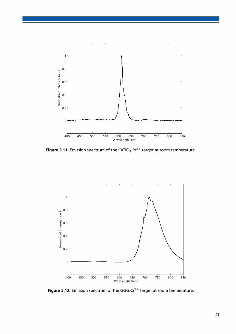
400 450 500 550 600 650 700 750 800 850
0
0.2
0.4
0.6
0.8
1
Wavelength (nm)
Nor
mal
ized
Int
ensi
ty (
a.u)
Figure 5.11: Emission spectrum of the CaTiO3:Pr3+ target at room temperature.
400 450 500 550 600 650 700 750 800 850
0
0.2
0.4
0.6
0.8
1
Wavelength (nm)
Nor
mal
ized
Int
ensi
ty (
a.u.
)
Figure 5.12: Emission spectrum of the GGG:Cr3+ target at room temperature.
41

5.3.2 Temperature-dependent luminescence characteristics
Figure 5.13 presents the temperature-lifetime characteristic for the CaTiO3:Pr3+ thin film deposited onthe stainless steel substrate. Brübach et al. [77] measured the temperature-lifetime characteristic of aCaTiO3:Pr3+ powder sample with the same Pr3+ doping concentration as of the present study and theirresults are also included in Figure 5.13. The calibration curve of the film shows a fairly linear behaviorin the semilogarithmic plot. The lifetime starts from 1.55 × 10⁻⁶ s at 310 K and decreases down to4.60 × 10−7 at 500 K. The parameters c1 = 0.3 and c2 = 1.4 were used for the iterative fitting windowalgorithm. It was not possible to fit values of the lifetime at temperatures higher than 500 K due to lowsignal-to-noise ratio. Although, the lifetime of the thin film has a sensitivity in the observed tempera-ture range, it is comparatively low with respect to the previous studies on CaTiO3:Pr3+ powders [77].Differences in the setups for the signal collection could explain the differences between the film and thepowder results, as stated below.
The luminescence signal in [77] was measured using an interference filter at 610 nm and it was tempo-rally resolved with an input resistance of 50 Ω. However, in the present study, when the decay waveformswere collected with 50 Ω and with a 610 nm filter, the signals were almost lost due to the weak emissionfrom the film. The use of a higher resistance (500 Ω) could contribute to the attenuation of the calibra-tion curve due to the cutoff frequency effect. On the other hand, when the measurements are carriedout without an interference filter, light from different wavelengths could affect the decay waveform andtherefore the lifetime values.
However, since it is unlikely to obtain exactly the same stoichiometric in the film as in the target whenusing sputtering [63], the film could have a different doping concentration and therefore different lu-minescence characteristics, which could also contribute to the difference in lifetimes of the film and thepowder. Unfortunately, the determination of the Pr3+ doping concentration in the film was beyond theaims of the present study.
300 350 400 450 50010
-7
10-6
10-5
10-4
Temperature (K)
Life
tim
e (s
)
CaTiO3:Pr film
CaTiO3:Pr Powder [77]
Figure 5.13: Temperature-lifetime characteristic of the CaTiO3:Pr3+ film.
42
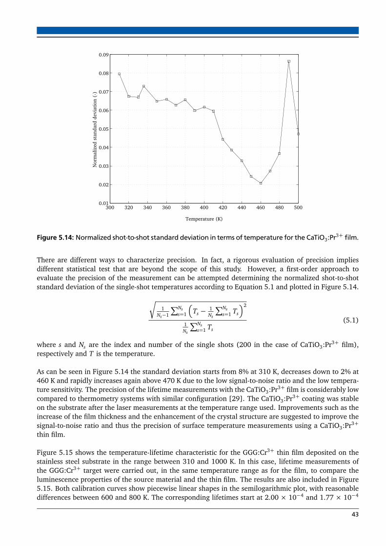
300 320 340 360 380 400 420 440 460 480 5000.01
0.02
0.03
0.04
0.05
0.06
0.07
0.08
0.09
Temperature (K)
Nor
mal
ized
sta
ndar
d de
viat
ion
(-)
Figure 5.14: Normalized shot-to-shot standard deviation in terms of temperature for the CaTiO3:Pr3+ film.
There are different ways to characterize precision. In fact, a rigorous evaluation of precision impliesdifferent statistical test that are beyond the scope of this study. However, a first-order approach toevaluate the precision of the measurement can be attempted determining the normalized shot-to-shotstandard deviation of the single-shot temperatures according to Equation 5.1 and plotted in Figure 5.14.
Ç
1Ns−1
∑Nss=1
Ts −1Ns
∑Nss=1 Ts
2
1Ns
∑Nss=1 Ts
(5.1)
where s and Ns are the index and number of the single shots (200 in the case of CaTiO3:Pr3+ film),respectively and T is the temperature.
As can be seen in Figure 5.14 the standard deviation starts from 8% at 310 K, decreases down to 2% at460 K and rapidly increases again above 470 K due to the low signal-to-noise ratio and the low tempera-ture sensitivity. The precision of the lifetime measurements with the CaTiO3:Pr3+ film is considerably lowcompared to thermometry systems with similar configuration [29]. The CaTiO3:Pr3+ coating was stableon the substrate after the laser measurements at the temperature range used. Improvements such as theincrease of the film thickness and the enhancement of the crystal structure are suggested to improve thesignal-to-noise ratio and thus the precision of surface temperature measurements using a CaTiO3:Pr3+
thin film.
Figure 5.15 shows the temperature-lifetime characteristic for the GGG:Cr3+ thin film deposited on thestainless steel substrate in the range between 310 and 1000 K. In this case, lifetime measurements ofthe GGG:Cr3+ target were carried out, in the same temperature range as for the film, to compare theluminescence properties of the source material and the thin film. The results are also included in Figure5.15. Both calibration curves show piecewise linear shapes in the semilogarithmic plot, with reasonabledifferences between 600 and 800 K. The corresponding lifetimes start at 2.00 × 10⁻⁴ and 1.77 × 10⁻⁴
43

at 310 K and decrease to 2.50 × 10⁻⁷ and 2.29 × 10⁻⁷ at 1000 K for the thin film and the target, re-spectively. The parameters c1 = 0.5 and c2 = 3.5 for the iterative fitting window algorithm yielded goodresults in terms of precision. The temperature sensitivities of the lifetimes are similar to those reportedfor a GGG:Cr3+ coating applied by air-brush on a stainless steel substrate [9], which were measuredwith similar setup and parameters as of the present study. The differences between the thin film and thetarget could be due to the inherent change in the stoichiometric (i.e. in the Cr3+ doping concentration)during the sputtering deposition.
The normalized shot-to-shot standard deviations of the single-shot temperatures calculated with Equa-tion 5.1 (with Ns = 100 shots) are presented in Figure 5.16. The GGG:Cr3+ thin film provides standarddeviations below 0.65% for the whole temperature range resulting in a high precision of the same orderas the previous study of Fuhrmann et al. [9] for a thick GGG:Cr3+ coating (∼10 µm). The target’sprecision behavior is similar, with an increase in standard deviations above 930 K. The variation of theprecision at high temperatures could be related with two effects: (1) at short lifetimes, the trigger hasa major disturbing influence on the decay waveform, decreasing the signal-to-noise ratio; (2) The thelow-pass characteristics (cut-off frequency) of the detection system decrease the sensitivity at high tem-peratures, affecting the precision.
300 400 500 600 700 800 900 100010
-7
10-6
10-5
10-4
10-3
Temperature (K)
Life
tim
e (s
)
GGG:Cr thin filmGGG:Cr target
Figure 5.15: Temperature-lifetime characteristics of the GGG:Cr3+ film and target.
The results of temperature sensitivity and precision prove the feasibility of high-precision zero-dimensional single-shot temperature measurements using a thin film of GGG:Cr3+ in the range from310 to 1000 K and its the most important result of this research. The GGG:Cr3+ coating was stable onthe substrate after the laser measurements at different temperatures. However, because of the differ-ences on the lifetimes of the film and the source material (target) can result in temperature differencesas high as 20 K, it is recommended to construct calibration curves for every coating produced by sputter-ing deposition.
44

300 400 500 600 700 800 900 10000
0.005
0.01
0.015
0.02
0.025
Temperature (K)
Nor
mal
ized
sta
ndar
d de
viat
ion
(-)
GGG:Cr thin filmGGG:Cr target
Figure 5.16: Normalized shot-to-shot standard deviations in terms of temperature for the GGG:Cr3+ filmand target.
5.3.3 Spatially resolved lifetime characteristics
Two-dimensional luminescence lifetime measurements of the GGG:Cr3+ film were performed at roomtemperature (293 K) to evaluate the spatial homogeneity of the luminescence characteristics of the de-posited films. This measurement was not possible with the CaTiO3:Pr3+ film due to its low emissionintensity. Although, it is beyond the original scope of this thesis, this analysis increases the understand-ing of the characteristics of the phosphor thin films produced by sputtering. In this way, opportunitiesfor future studies can be identified.
Figure 5.17 presents the two-dimensional spatial distribution of the lifetime of the GGG:Cr3+ film atroom temperature. The non-uniformities at the edges of the coating result from the "shadow" generatedby the thickness of the substrate holder during the sputtering process. Clear spatial inhomogeneities ofthe luminescence lifetime of the GGG:Cr3+ film are observed. As quantified in Figure 5.18, there is arelative broad distribution of lifetimes in the film. At room temperature, a difference of 1 × 10⁻⁵ s inlifetime results in a ∆T of ∼10 K. Therefore, it could be considered that the film has a relative poorspatial homogeneity of luminescence properties.
Figure 5.19 displays the initial intensity of the luminescence emission of the GGG:Cr3+ film at 293 K. Theinhomogeneities on intensity could be due to non-uniformities of the laser beam profile, inhomogeneitiesof the film thickness, or any other physical defects of the film. However, this does not explain the spatialinhomogeneity of the luminescence lifetime as similar patterns between Figures 5.17 and 5.19 can notbe identified when comparing both figures. As a consequence, local differences in doping concentrationcould be the reason for such an inhomogeneity on lifetimes. From the sputtering process it is unliketo obtain such a random distribution of Cr3+ atoms [63]. However, during the annealing process, localdifferences in the crystallinity of the film, due to temperature gradients, and/or Cr diffusion from the
45

stainless steel substrate, due to the high temperature, could explain the luminescence characteristics ofthe film.
Pixel
Pixe
lLifetime (s)
20 40 60 80 100
20
40
60
80
100
1202.1
2.2
2.3
2.4
2.5
2.6
2.7
2.8
2.9
x 10-4
Figure 5.17: 2D luminescence lifetime of the GGG:Cr3+ film at room temperature.
2.0 2.1 2.2 2.3 2.4 2.5 2.6 2.7 2.8 2.90
5
10
15
20
25
30
35
Lifetimes (s)
Perc
enta
ge o
f are
a (%
)
x 10-4
Figure 5.18: Distribution of lifetimes in the GGG:Cr3+ film at room temperature.
46

The sputtering deposition of films with larger thicknesses, the increase of the maximum temperatureof the annealing, and the coating of substrates without Cr content are suggested for future studies onGGG:Cr3+ thin films. Additionally, studies of the morphology of the films by scanning electron mi-croscopy (SEM) or atomic force spectroscopy (AFM) and the use of surface characterization techniquesthat allow measuring local doping concentrations such as Rutherford backscattering spectroscopy (RBS)or particle-induced X-ray emission spectrometry (PIXE) are highly recommended.
Pixel
Pixe
l
Intensity (a.u.)
20 40 60 80 100
20
40
60
80
100
120 400
600
800
1000
1200
1400
1600
1800
2000
Figure 5.19: Initial intensity distribution of luminescence emission from the GGG:Cr3+ film at room tem-perature.
5.4 Results on GGG:Cr3+ powders
5.4.1 Crystal structures
As in 5.3.3, this section is beyond the scope of the thesis, however it is presented intending to improve theinsight on the luminescence properties of the GGG:Cr3+ phosphor. Figure 5.20 shows the XRD patternsof the GGG:Cr3+ powders with different doping concentrations and co-doped with Ce as a way to reducethe afterglow. The diffraction patterns are consistent with the cubic garnet single phase Gd3Ga5O12 ICSD9237 [70]. All the reflections in the range 10 < 2θ < 90 are sharper and more developed than thosefrom the GGG:Cr3+ target (Figure 5.5). Variations in background are due to differences on the amountof powder used for each sample. The second phase of Gd3GaO6 is not present in any of the patterns. Thismeans that the sintering of the powders up to 1673 K yields single phase GGG:Cr3+ with high crystallinity.
47

0
20
40
60
80
100
Rel
ativ
e In
tens
ity
(a.u
.)
10 20 30 40 50 60 70 80 900
50
100
2 θ
ICSD 9237
GGG:Cr (0.5 mol%), Ce (0.038 %w)GGG:Cr (0.5 mol%), Ce (0.114 %w)GGG:Cr (0.125 mol%)GGG:Cr (0.25 mol%)GGG:Cr (0.5 mol%)GGG:Cr (1 mol%)GGG:Cr (2 mol%)
(2 1 1)(3 2 1)
(4 0 0)
(4 2 0)
(4 2 2)
(5 2 1) (6 1 1) (4 4 4)
(6 4 0)
(6 4 2)
(8 0 0)(8 4 0)(8 4 2)
(6 4 4)
(10 4 0)
(8 8 0)
Figure 5.20: XRD patterns of the GGG:Cr3+ powder samples with different doping concentrations alongwith the GGG:Cr3+ samples co-doped with Ce.
5.4.2 Effect of doping concentration on the temperature-dependent luminescence properties
To study the effect of doping concentration on the temperature-dependent luminescence properties ofGGG:Cr3+, measurements of the lifetimes of powder samples with Cr concentrations of 0.125, 0.25, 0.5,1, and 2 mol% were carried out in the range from 480 to 670 K. The results, obtained with the parame-ters c1 = 0.5 and c2 = 3.5 for the iterative fitting window algorithm, are plotted in Figure 5.21. At lowdoping concentrations there is not a clear effect of the Cr concentration on the luminescence lifetime.However, the luminescence lifetime decreases with the increase of the Cr concentration from 0.5 mol%,probably due to concentration quenching [7]. Although, the lifetimes are shifted when varying the dop-ing concentration, the temperature sensitivities of the lifetimes are similar in this temperature range.
The normalized shot-to-shot standard deviations of the single-shot temperatures, calculated with Equa-tion 5.1, for the samples with different doping concentrations are presented in Figure 5.22. The fiveGGG:Cr3+ samples provide standard deviations below 0.45% within the observed temperature range.Therefore, the selection of the doping concentration is not expected to affect the precision of the ther-mographic system to perform single-shot temperature measurements.
48

480 500 520 540 560 580 600 620 640 660 680
10-5
10-4
Temperature (K)
Life
tim
e (s
)
GGG:Cr (0.125 mol%)GGG:Cr (0.25 mol%)GGG:Cr (0.5 mol%)GGG:Cr (1 mol%)GGG:Cr (2 mol%)
Figure 5.21: Temperature-lifetime characteristics of the GGG:Cr3+ powder samples with different dopingconcentrations.
480 500 520 540 560 580 600 620 640 660 6800.5
1
1.5
2
2.5
3
3.5
4
4.5x 10
-3
Temperature (K)
Nor
mal
ized
sta
ndar
d de
viat
ion
(-)
GGG:Cr (0.125 mol%)GGG:Cr (0.25 mol%)GGG:Cr (0.5 mol%)GGG:Cr (1 mol%)GGG:Cr (2 mol%)
Figure 5.22: Normalized shot-to-shot standard deviations in terms of temperature for the GGG:Cr3+ pow-der samples with different doping concentrations.
49

5.4.3 Effect of co-doping with Ce on the temperature-dependent luminescence properties
The effect of co-doping with small amounts of Ce on the temperature-dependent luminescence proper-ties of the GGG:Cr3+ was studied in the range from 480 to 670 K. Figure 5.23 presents the results ofthe luminescence lifetime of the GGG:Cr3+ sample with 0.5 mol% Cr content, along with the samplesco-doped with 0.038 and 0.114 %w Ce. The parameters c1 = 0.5 and c2 = 3.5 were used for the iterativefitting window algorithm. As can be seen, the sample co-doped with 0.038 %w Ce has similar lifetimecharacteristics than the GGG:Cr3+ sample without Ce content. However, the increase of the Ce contentup to 0.114 %w produces an irregular change in the lifetime values between 480 and 560 K, probablydue to a major role of Ce transitions in the luminescences characteristics of the phosphor. To clarifythis, the averaged normalized decays of the luminescence signals at 510 and 620 K are plotted in Figure5.24. As can be observed, the luminescence decay at 510 K is highly multi-exponential, particularly until∼100 µs. Therefore the fitting was carried out including this section of the decay, affecting the valuesof τ. Whereas, at 620 K, the highly multi-exponential part of the decay is shorter, affecting less thefitting. To overcome this, the parameters of the fitting algorithm were changed to c1 = 1.7 and c2 =3.9, expecting to fit the lifetimes at sections where the decay shows fairly mono-exponential characteris-tics. As shown in Figure 5.23, with the change of the fitting parameters, a calibration curve with similarsensitivity as those of GGG:Cr3+ (0.5 mol%) and GGG:Cr3+ (0.5 mol%), Ce (0.038 %w) can be obtained.
480 500 520 540 560 580 600 620 640 660 680
10-5
10-4
Temperature (K)
Life
tim
e (s
)
GGG:Cr (0.5 mol%) C1=0.5, C
2=3.5
GGG:Cr (0.5 mol%), Ce (0.038 %w) C1=0.5, C
2=3.5
GGG:Cr (0.5 mol%), Ce (0.114 %w) C1=0.5, C
2=3.5
GGG:Cr (0.5 mol%), Ce (0.114 %w) C1=1.7, C
2=3.9
Figure 5.23: Temperature-lifetime characteristics of the GGG:Cr3+ powder samples co-doped with Ce.
The precision of the measurements decreases when co-doping with a high content of Ce. As can beseen in Figure 5.25, the normalized shot-to-shot standard deviation of the GGG:Cr3+ sample co-dopedwith 0.114 %w Ce is higher than 1%, particularly at temperatures between 480 and 540 K, while thevalues of the GGG:Cr3+ (0.5 mol%) and GGG:Cr3+ (0.5 mol%), Ce (0.038 %w) samples are lower than0.5% in the whole range studied. Finally, as can be deduced from Figure 5.26, two improvements in theluminescence properties of GGG:Cr3+ by co-doping with small amounts of Ce could be obtained: (1) thedecay of the luminescence signal is fairly mono-exponential, which is favorable for the fitting of lifetimevalues and (2) the luminescent afterglow is decreased in agreement with Greskovich et al. [78]. This
50

could be highly beneficial for example for high speed temperature measurements since the base lines ofthe decay waveforms would not strongly change during the sampling.
0 100 200 300 400 500 60010
-8
10-6
10-4
10-2
100
Time(µs)
Nor
mal
ized
Int
ensi
ty (
a.u)
510K620K
Figure 5.24: Normalized decays of the luminescence signals of the GGG:Cr3+ (0.5 mol%), Ce (0.114 %w)sample at 510 and 620 K.
480 500 520 540 560 580 600 620 640 660 6800
0.005
0.01
0.015
0.02
0.025
0.03
0.035
0.04
Temperature (K)
Nor
mal
ized
sta
ndar
d de
viat
ion
(-)
GGG:Cr (0.5 mol%) C1=0.5, C
2=3.5
GGG:Cr (0.5 mol%), Ce (0.038 %w) C1=0.5, C
2=3.5
GGG:Cr (0.5 mol%), Ce (0.114 %w) C1=1.7, C
2=3.9
Figure 5.25: Normalized shot-to-shot standard deviations in terms of temperature for the GGG:Cr3+ pow-der samples co-doped with Ce.
51

0 50 100 150 200 250 300 350 40010
-8
10-6
10-4
10-2
100
Time (µs)
Nor
mal
ized
Int
ensi
ty (
a.u)
GGG:Cr (0.5 mol%)GGG:Cr (0.5 mol%), Ce (0.038 %w)
Figure 5.26: Normalized decays of the luminescence signals of the GGG:Cr3+ (0.5 mol%), and theGGG:Cr3+ (0.5 mol%), Ce (0.038 %w) samples at 670 K.
52

6 Concluding Remarks and OutlookStable thin films of praseodymium-doped calcium titanate, CaTiO3:Pr3+, and chromium-doped gadolin-ium gallium oxide, Gd3Ga5O12:Cr3+ have been successfully deposited on stainless steel substrates byradio frequency magnetron sputtering. The physical, chemical, and luminescence properties of the phos-phor films have been evaluated for thermographic purposes. Experiments in Gd3Ga5O12:Cr3+ powders,varying the doping concentration and evaluating the effect of co-doping with cerium, have been in-cluded. From the results, their analysis and discussion, the following conclusions and outlook can bestated:
With appropriate handling, stable sputtering targets of CaTiO3:Pr3+ and Gd3Ga5O12:Cr3+ can be pre-pared by sol-gel combustion and solid-state reactions, respectively, combined with high temperaturesintering. However, their thermal and mechanical strength limited the performance of the sputteringprocess and, therefore, decreased the deposition rate of the films, increasing significantly the time re-quired for the deposition. It is recommended to sinter the targets at temperatures around 1800 K toenhance their properties, making them suitable for high-power sputtering deposition and reducing thedeposition time.
The physical and chemical characterization of the films allowed determining that the annealing pro-cess is necessary to restore the crystal structure and the luminescence characteristics of phosphor filmsdeposited by sputtering. Phosphors of complex crystal structures, such as Gd3Ga5O12:Cr3+, require an-nealing at high temperatures during several hours. This could represent a limitation for the applicabilityof sputtering to thermographic phosphors because some substrate materials could not resist annealingat high temperatures. In consequence, it is recommended to explore the use of advanced annealingprocesses such as laser annealing.
The functionality of the thin films of thermographic phosphors was evaluated at different tempera-tures by determining the luminescence characteristics under laser excitation. The CaTiO3:Pr3+ thinfilm showed a weak emission, resulting in low signal-to-noise ratios and poor temperature-dependentluminescence properties. Although the film exhibited fast luminescence decays, the low temperaturesensitivity and poor precision could limit the use of CaTiO3:Pr3+ thin films for thermography applica-tions.
In the case of the Gd3Ga5O12:Cr3+, the thin film exhibited a strong luminescence signal, fast lumines-cence decays, and appropriate temperature sensitivity in a relative wide range of temperatures (from 310to 1000 K), with adequate precision of the temperature determination. However, when two-dimensionalluminescence properties were evaluated, the film showed spatial inhomogeneities in the luminescencelifetime at room temperature, suggesting local differences of activator concentration in the film. Thinfilms of Gd3Ga5O12:Cr3+ proved to be suitable for point temperature measurements. Nevertheless, itsapplication for spatially resolved temperature measurements would require further studies, for example,of the effects of the main parameters involved in sputtering deposition on the final functionality of thefilm. Moreover, multidimensional surface characterization of the thin films, that allow relating theirphysical and chemical properties with their spatial luminescence properties, is highly recommended.
Finally, the experiments in Gd3Ga5O12:Cr3+ powders samples revealed that variations in doping con-centration of Cr3+ only change significantly the luminescence lifetime at concentrations above 1 mol%,
53

while sensitivity and precision of the temperature determination are maintained. Co-doping with smallamounts of cerium reduces the afterglow and produces fairly mono-exponential luminescence decays.However, an excess of cerium affects significantly the luminescence properties of Gd3Ga5O12:Cr3+, re-sulting in highly multi-exponential decays and poor precision of the temperature determination.
54

Bibliography[1] A. G. Evans, D. R. Mumm, J. W. Hutchinson, G. H. Meier, and F. S. Pettit. Mechanisms controlling
the durability of thermal barrier coatings. Progress in Materials Science, 46(5):505–553, 2001.
[2] K. M. Kim, N. Yun, Y. H. Jeon, D. H. Lee, and H. H. Cho. Failure analysis in after shell section of gasturbine combustion liner under base-load operation. Engineering Failure Analysis, 17(4):848–856,2010.
[3] P. R. N. Childs, J. R. Greenwood, and C. A. Long. Review of temperature measurement. Review ofScientific Instruments, 71(8):2959–2978, 2000.
[4] J. Brübach, M. Hage, J. Janicka, and A. Dreizler. Simultaneous phosphor and CARS thermometry atthe wall-gas interface within a combustor. Proceedings of the Combustion Institute, 32(1):855–861,2009.
[5] J. A. Stasiek and T. A. Kowalewski. Thermochromic liquid crystals in heat transfer research. Proc.SPIE 4759, XIV Conference on Liquid Crystals: Chemistry, Physics, and Applications, pages 374–383,2002.
[6] T. Liu, B. T. Campbell, S. P. Burns, and J. P. Sullivan. Temperature- and pressure-sensitive lumines-cent paints in aerodynamics. Applied Mechanics Reviews, 50(4):227–246, 1997.
[7] A. Khalid and K. Kontis. Thermographic phosphors for high temperature measurements: Principles,current state of the art and recent applications. Sensors, 8(9):5673–5744, 2008.
[8] J. Brübach, J. Janicka, and A. Dreizler. An algorithm for the characterization of multi-exponentialdecay curves. Optics and Lasers in Engineering, 47(1):75–79, 2009.
[9] N. Fuhrmann, T. Kissel, A. Dreizler, and J. Brübach. Gd3Ga5O12:Cr—a phosphor for two-dimensional thermometry in internal combustion engines. Measurement Science and Technology,22(4):045301, 2011.
[10] J. Brübach, E. Van Veen, and A. Dreizler. Combined phosphor and CARS thermometry at thewall-gas interface of impinging flame and jet systems. Experiments in Fluids, 44(6):897–904, 2008.
[11] J. P. Feist, A. L. Heyes, and S. Seefelt. Thermographic phosphor thermometry for film coolingstudies in gas turbine combustors. Proceedings of the Institution of Mechanical Engineers, Part A:Journal of Power and Energy, 217(2):193–200, 2003.
[12] A. Omrane, F. Ossler, M. Aldén, J. Svenson, and J. B. C. Pettersson. Surface temperature of de-composing construction materials studied by laser-induced phosphorescence. Fire and Materials,29(1):39–51, 2005.
[13] S. W. Allison, M. R. Gates, D. L. Beshears, and G. T. Gillies. Phosphor thermometry at ORNL. AIPConference Proceedings, 684(1):1033–1038, 2003.
[14] A. M. Murray and L. A. Melton. Fluorescence methods for determination of temperature in fuelsprays. Applied Optics, 24(17):2783–2787, 1985.
[15] A. Omrane, F. Ossler, and M. Aldén. Two-dimensional surface temperature measurements of burn-ing materials. Proceedings of the Combustion Institute, 29(2):2653–2659, 2002.
55

[16] N. Fuhrmann, M. Schild, D. Bensing, S. Kaiser, C. Schulz, J. Brübach, and A. Dreizler. Two-dimensional cycle-resolved exhaust valve temperature measurements in an optically accessibleinternal combustion engine using thermographic phosphors. Applied Physics B: Lasers and Op-tics, 106:945–951, 2012.
[17] J. Ervin, C. Murawski, C. MacArthur, M. Chyu, and D. Bizzak. Temperature measurementof a curved surface using thermographic phosphors. Experimental Thermal and Fluid Science,11(4):387–394, 1995.
[18] H. Aizawa, M. Sekiguchi, T. Katsumata, S. Komuro, and T. Morikawa. Fabrication of ruby phosphorsheet for the fluorescence thermometer application. Review of Scientific Instruments, 77(4):044902,2006.
[19] S. S. Azim, C. Solaiyan, and G. Venkatachari. Development of coating for temperature sensing.Progress in Organic Coatings, 62(1):28 – 31, 2008.
[20] S. W. Allison, D. L. Beshears, T. Gadfort, T. Bencic, J. Eldridge, W. A. Hollerman, and P. Boudreaux.High temperature surface measurements using lifetime imaging of thermographic phosphors:bonding tests. ICIASF Record, International Congress on Instrumentation in Aerospace SimulationFacilities, pages 171–176, 2001.
[21] S. M. Goedeke, W. A. Hollerman, N. P. Bergeron, S. W. Allison, M. R. Cates, T. J. Bencic, C. R.Mercer, and J. I. Eldridge. Study of Resbond®Ceramic binders used for high temperature non-contactthermometry, pages 115–125. John Wiley & Sons, Inc., 2006.
[22] S. Alaruri, D. McFarland, A. Brewington, M. Thomas, and N. Sallee. Development of a fiber-optic probe for thermographic phosphor measurements in turbine engines. Optics and Lasers inEngineering, 22(1):17 – 31, 1995.
[23] I. P. McClean, A. J. Simons, C. B. Thomas, and J. E. Mutton. Comparison between thin film andbonded powder phosphors for thermographic sensing in gas turbine engines. IEEE Trans InstrumMeas, 49(1):129–131, 2000.
[24] R. M. Ranson, C. B. Thomas, and M. R. Craven. A thin film coating for phosphor thermography.Measurement Science and Technology, 9(12):1947, 1998.
[25] H. Seyfried, G. Sarner, A. Omrane, M. Richter, H. Schmidt, and M. Alden. Optical diag-nostics for characterization of a full-size fighter-jet afterburner. ASME Conference Proceedings,2005(46997):813–819, 2005.
[26] H. Seyfried, M. Richter, M. Aldén, and H. Schmidt. Laser-induced phosphorescence for surfacethermometry in the afterburner of an aircraft engine. AIAA Journal, 45(12):2966–2971, 2007.
[27] J. Armfield, R. Graves, D. Beshears, M. Cates, T. V. Smith, and S. W. Allison. Phosphor thermometryfor internal combustion engines. SAE Technical Paper 971642, 1997.
[28] W. Kern and K. K. Schuegraf. 1 - Deposition technologies and applications: introduction and overview,pages 11–43. William Andrew Publishing, Norwich, NY, 2001.
[29] J. Brübach, C. Pflitsch, A. Dreizler, and B. Atakan. On surface temperature measurements withthermographic phosphors: a review. Progress in Energy and Combustion Science, 39:37–60, 2013.
[30] A. C. Pierre. Introduction to sol–gel processing. Kluver Academic Publishers, Boston, 1998.
[31] A. Nebatti, C. Pflitsch, C. Eckert, and B. Atakan. Sol–gel-deposition of thin TiO2:Eu3+ thermo-graphic phosphor films. Progress in Organic Coatings, 67(3):356 – 360, 2010.
56
[32] C. Pflitsch, R. A. Siddiqui, C. Eckert, and B. Atakan. Sol–gel deposition of chromium doped alu-minium oxide films (ruby) for surface temperature sensor application. Chemistry of Materials,20(8):2773–2778, 2008.
[33] C. Pflitsch, D. Viefhaus, and B. Atakan. CVD of thin ruby films on Si(100) and stainless steel forsurface temperature sensor applications. Chemical Vapor Deposition, 13(8):420–426, 2007.
[34] C. Eckert, C. Pflitsch, and B. Atakan. Dy3+:Al2O3 and (Dy3+, Cr3+): Al2O3 films for temperaturesensor applications derived by thermal cvd and sol-gel techniques. ECS Transactions, 25(8):1293–1300, 2009.
[35] K. L. Choy, J. P. Fesit, A. L. Heyes, and B. Su. Eu-doped Y2O3 phosphor films produced byelectrostatic-assisted chemical vapor deposition. Journal of Materials Research, 14:3111–3114,1999.
[36] M. M. Gentleman, J. I. Eldridge, D. M. Zhu, K. S. Murphy, and D. R. Clarke. Non-contact sens-ing of TBC/BC interface temperature in a thermal gradient. Surface and Coatings Technology,201(7):3937–3941, 2006.
[37] R. J. L. Steenbakker, R. G. Wellman, J. R. Nicholls, and J. P. Feist. Sensor TBCs: remote in-situcondition monitoring of EB-PVD coatings at elevated temperatures. ASME Conference Proceedings,2008(43116):269–278, 2008.
[38] U. Gibson and M. Chernuschenko. Ruby films as surface temperature and pressure sensors. Opt.Express, 4(11):443–448, 1999.
[39] X. Chen, Z. Mutasim, J. Price, J. P. Feist, A. L. Heyes, and S. Seefeldt. Industrial sensor TBCs: stud-ies on temperature detection and durability. International Journal of Applied Ceramic Technology,2(5):414–421, 2005.
[40] S. Rossnagel and K. Seshan. 8 - Sputtering and sputter deposition, pages 319–348. William AndrewPublishing, Norwich, NY, 2001.
[41] T. Minami, T. Nakatani, T. Miyata, and T. Shirai. (Y2O3–GeO2) phosphor thin-film electrolumi-nescent emitting layers prepared by magnetron sputtering. Surface and Coatings Technology, 146–147(0):508–512, 2001.
[42] S. M. Chung, S. H. Han, and Y. J. Kim. Characterization of compositional variation and lumines-cence of ZnGa2O4:Mn thin film phosphor. Materials Letters, 59(7):786–789, 2005.
[43] T. K. Tran, W. Park, J. W. Tomm, B. K. Wagner, S. M. Jacobsen, C. J. Summers, P. N. Yocom, and S. K.McClelland. Photoluminescence properties of ZnGa2O4:Mn powder phosphors. Journal of AppliedPhysics, 78(9):5691–5695, 1995.
[44] H. Song and Y. J. Kim. Characterization of luminescent properties of ZnO:Er thin films prepared byrf magnetron sputtering. Journal of the European Ceramic Society, 27(13–15):3745–3748, 2007.
[45] T. Miyata, J. Ishino, K. Sahara, and T. Minami. Color control of emissions from rare earth-co-dopedLa2O3:Bi phosphor thin films prepared by magnetron sputtering. Thin Solid Films, 519(22):8095–8099, 2011.
[46] J. P. Chu, I. J. Hsieh, J. T. Chen, and M. S. Feng. Growth of MgWO4 phosphor by rf magnetronsputtering. Materials Chemistry and Physics, 53(2):172–178, 1998.
[47] J. Kim and K. Yoon. Influence of post-deposition annealing on the microstructure and propertiesof Ga2O3:Mn thin films deposited by rf planar magnetron sputtering. Journal of Materials Science:Materials in Electronics, 20(9):879–884, 2009.
57

[48] D. Kim, S. Choi, C. Park, and B. O. Luminescence characteristics of ZnS:Cu thin film electrolu-minescent devices fabricated by sputtering. Journal of Materials Science: Materials in Electronics,9(1):31–34, 1998.
[49] C. Chartier, C. Barthou, P. Benalloul, S. Chenot, and J. M. Frigerio. Structural and luminescentproperties of green emitting SrGa2S4:Eu thin films prepared by rf-sputtering. Journal of CrystalGrowth, 256(3–4):305–316, 2003.
[50] E. J. Bosze, G. A. Hirata, and J. McKittrick. An analysis of Y2O3:Eu3+ thin films for thermographicphosphor applications. Journal of Luminescence, 131(1):41–48, 2011.
[51] L. Sarakha, T. Bégou, A. Goullet, J. Cellier, A. Bousquet, E. Tomasella, T. Sauvage, P. Boutinaud, andR. Mahiou. Influence of synthesis conditions on optical and electrical properties of CaTiO3:Pr3+ thinfilms deposited by radiofrequency sputtering for electroluminescent device. Surface and CoatingsTechnology, 205, Supplement 2(0):S250–S253, 2011.
[52] S. M. Chung, S. H. Han, K. H. Song, E. S. Kim, and Y. J. Kim. Luminescent properties of CaTiO3:Prthin-film phosphor deposited on ZnO/ITO/glass substrate. Journal of Luminescence, 114(3–4):227–233, 9 2005.
[53] L. Sarakha, A. Bousquet, E. Tomasella, P. Boutinaud, and R. Mahiou. Investigation of CaTiO3:Pr3+
thin films deposited by radiofrequency reactive magnetron sputtering for electroluminescence ap-plication. Materials Science and Engineering Conference Series, 12(1):012008, 2010.
[54] E. Pinel, P. Boutinaud, and R. Mahiou. What makes the luminescence of Pr3+ different in CaTiO3and CaZrO3? Journal of Alloys and Compounds, 380(1–2):225–229, 2004.
[55] S. Fukaya, K. Adachi, M. Obara, and H. Kumagai. The growth of Cr4+:YAG and Cr4+:GGG thinfilms by pulsed laser deposition. Optics Communications, 187(4–6):373–377, 2001.
[56] M. S. B. Darby, T. C. May-Smith, R. W. Eason, T. Donnelly, J. G. Lunney, and K. D. Rogers. Acomparative study of gadolinium gallium garnet growth by femtosecond and nanosecond pulsedlaser deposition. Applied Surface Science, 254(11):3364–3369, 2008.
[57] X. Xu, Z. Xu, Y. Hou, X. Wang, X. Chen, and X. Xu. A novel blue thin film electroluminescentphosphor Gd3Ga5O12:Ag. Chinese Physics Letters, 16(5):387, 1999.
[58] X. Xu, Z. Xu, Y. Hou, Y. Wang, and X. Xu. Influence of Ag concentration and post-depositionannealing on Gd3Ga5O12:Ag thin film electroluminescence. Displays, 22(3):97–100, 2001.
[59] C. Gheorghies, P. Boutinaud, M. Loic, and V.O. Atanasiu. Results on nanosized CaTiO3:Pr3+ phos-phor. Journal of optoelectronics and advanced materials, 11(5):583–589, 2009.
[60] P. Boutinaud, E. Pinel, M. Dubois, A. P. Vink, and R. Mahiou. UV-to-red relaxation pathways inCaTiO3:Pr3+. Journal of Luminescence, 111(1–2):69–80, 2005.
[61] R. Martín-Rodríguez. Synthesis, structural characterization and spectroscopic study of nanocrystallineand microcrystralline materials. PhD thesis, Universidad de Cantabria, 2010.
[62] U. Hömmerich and K. L. Bray. High-pressure laser spectroscopy of Cr3+:Gd3Sc2Ga5O12 andCr3+:Gd3Ga5O12. Physical Review B, 51(18):12133–12141, 1995.
[63] B. Chapman. Glow discharge processes: sputtering and plasma etching. John Wiley & Sons, Inc., NewYork, 1980.
[64] STOE and Cie GmbH. STOE Version 1.1, 2002. http://www.stoe.com.
58

[65] Omicron NanoTechnology GmbH. Multiprobe surface science systems user’s guide. Project 094603,September, 2010.
[66] J. F. Moulder, W. F. Stickle, P. E. Sobol, and K. D. Bomben. Handbook of X-ray photoelectron spec-troscopy. Physical Electronics, Inc., Minnesota, 1995.
[67] N. Fuhrmann, J. Brübach, and A. Dreizler. Phosphor thermometry: a comparison of the lumi-nescence lifetime and the intensity ratio approach. Proceedings of the Combustion Institute, 2012.http://dx.doi.org/10.1016/j.proci.2012.06.084.
[68] M. A. Everest and D. B. Atkinson. Discrete sums for the rapid determination of exponential decayconstants. Review of Scientific Instruments, 79(2):023108–9, 2008.
[69] H. F. Kay and P. C. Bailey. Structure and properties of CaTiO3. Acta Crystallographica, 10(3):219–226, 1957.
[70] E.L. Dukhovskaya, Y.G. Saksonov, and A.G Titova. Neorganicheskie Materialy, 9:809–813, 1973.
[71] R. Martín-Rodríguez, R. Valiente, F. Rodríguez, and M. Bettinelli. Temperature and pressuredependence of the optical properties of Cr3+-doped Gd3Ga5O12 nanoparticles. Nanotechnology,22(26):265707, 2011.
[72] W. H. Chao, R. J. Wu, and T. B. Wu. Structural and luminescent properties of YAG:Ce thin filmphosphor. Journal of Alloys and Compounds, 506(1):98–102, 2010.
[73] G. J. Fischer, Z. Wang, and S. Karato. Elasticity of CaTiO3, SrTiO3 and BaTiO3 perovskites up to3.0 GPa: the effect of crystallographic structure. Physics and Chemistry of Minerals, 20(2):97–103,1993.
[74] Z. Wang, S. Karato, and K. Fujino. High temperature creep of single crystal gadolinium galliumgarnet. Physics and Chemistry of Minerals, 23(2):73–80, 1996.
[75] Casa Software Ltd. Manual of basic quantification of XPS spectra, 2011. http://www.casaxps.com/help_manual/manual_updates/xps_spectra.pdf.
[76] Casa Software Ltd. CasaXPS Version 2.3.16, 1999-2011. http://www.casaxps.com.
[77] J. Brübach, T. Kissel, M. Frotscher, M. Euler, B. Albert, and A. Dreizler. A survey of phosphors novelfor thermography. Journal of Luminescence, 131(4):559–564, 2011.
[78] C. Greskovich and S. Duclos. Ceramic scintillators. Annual Review of Materials Science, 27(1):69–88,1997.
59


