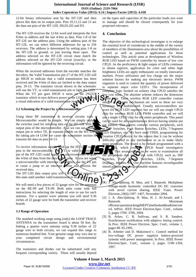
International Journal of Science and Research (IJSR) ISSN (Online): 2319-7064 Index Copernicus Value (2013): 6.14 | Impact Factor (2013): 4.438 Volume 4 Issue 3, March 2015 www.ijsr.net Licensed Under Creative Commons Attribution CC BY Development of Wireless RGB LED PWM Controller on Low Cost CPLD Kamal Kant Sharma 1 , Vipin Kumar Gupta 2 1 M.Tech, Suresh Gyan Vihar University, Jaipur, India 2 Assistant professor, Suresh Gyan Vihar University, Jaipur, India Abstract: This article aims at development of Wireless RGB LED based on PWM controller by means of low cost CPLD. As the proficiency & light output of LEDs continues to obtain superior, application for color and white high brightness LEDs are apply enthusiastic on totally innovative markets. Power utilization and low charge are the major solution factors for making any electronic device. PWM organizer is used to control the quantity of power delivered to separate major color LED’s. The incorporation of complete logic hooked on solitary chip CPLD satisfies the low cost issue. The absolute scheme reduces the dimension of the chip. These wireless RGB LED controller contain integer of separate mechanism are worn so these are very luxurious and multifaceted. Usually microcontrollers are worn for RGB LED regulator but we will use single CPLD chip for wireless RGB LED PWM controller and we will use a single CPLD chip for the entire peripherals. This panel can be used for all supplementary devices having similar pin out pattern. This pattern contains various peripherals, such as DIP Switches, Push Button Switches, LEDs, 7-Segment LED Displays, etc. We have used VHDL programming for creation CPLD device for the reason that it can be without difficulty ported to any mechanism so as to make likely mass invention. The board is by default programmed with a *.jam file, which contains CPLD board investigative System. This arrangement can be worn to examination all the peripherals that are on slat with CPLD, such as, DIP Switches, Push Button Switches, LEDs, 7-Segment Displays, headers, etc. Our machine features reconfigurable intend payable to reprogrammable reason. Keywords: CPLD, Low cost, LED 1. Introduction This purpose explains aspects of the assumption and put into practice of creating color-consistent, LED-based illumination yield .LEDs, as with all artificial products, have fabric and process variations that give way goods with matching dissimilarity in presentation. LEDs are binned and packaged to equilibrium the environment of the manufacturing process with the requests of the illumination manufacturing. Illumination-class LEDs are ambitious by application requirements and industry standards, including color steadiness and color and lumen preservation. Immediately as conventional lamps are sold by intensity (typically indicated by wattage) and color (warm or cool white), LEDs are binned for brightness (luminous flux) and color parameters (chromaticity). Figure 1.1: General Diagram of the CPLD Board 2. Application Design The CPLD timber (Entry Level Tool) is deliberate intended for the MAX Device (EPM3064). This board can be worn intended for any other device having comparable pin out pattern. The client is confident to make sure out the panel schematics for the more details. This board contains a variety of peripherals, such as DIP Switches, Push Button Switches, LEDs, 7-Segment LED Displays, etc. interfaced with the MAX Device. The slat is by defaulting automatic with a *.jam file, which contains CPLD Board indicative System. This system can be used to test all the peripherals that are on board with the CPLD, such as, DIP Switches, Push Button Switches, LEDs, 7Segment LED Displays, headers, etc. The second segment gives the in order about all the hardware mechanism and peripherals on this CPLD Board. The third segment gives the in sequence concerning the CPLD Board Diagnostic System that is surrounded within the CPLD. This segment gives facts concerning all the tests that can be done using this system and how to use this system for testing involved peripherals. The fourth segment gives indication mapping flanked by the CPLD and all the peripherals. The fifth segment indicates the position objects connected with this slat. This section gives the component details about the CPLD Board Hardware. This section describes all the peripherals that are integrated with the CPLD. The comprehensive figure of the CPLD Board is shown. As exposed in the figure, the board contains two 8-way DIP Switches, eight Push Button Switches, eight LEDs, two 7- Segment LED Displays, Connection headers for inputs and outputs (shared), JTAG header for downloading the bit files Paper ID: SUB152699 2177
Transcript
International Journal of Science and Research (IJSR) ISSN (Online): 2319-7064
Index Copernicus Value (2013): 6.14 | Impact Factor (2013): 4.438
Volume 4 Issue 3, March 2015
www.ijsr.net Licensed Under Creative Commons Attribution CC BY
Development of Wireless RGB LED PWM
Controller on Low Cost CPLD
Kamal Kant Sharma1, Vipin Kumar Gupta
2
1M.Tech, Suresh Gyan Vihar University, Jaipur, India
2Assistant professor, Suresh Gyan Vihar University, Jaipur, India
Abstract: This article aims at development of Wireless RGB LED based on PWM controller by means of low cost CPLD. As the
proficiency & light output of LEDs continues to obtain superior, application for color and white high brightness LEDs are apply
enthusiastic on totally innovative markets. Power utilization and low charge are the major solution factors for making any electronic
device. PWM organizer is used to control the quantity of power delivered to separate major color LED’s. The incorporation of complete
logic hooked on solitary chip CPLD satisfies the low cost issue. The absolute scheme reduces the dimension of the chip. These wireless
RGB LED controller contain integer of separate mechanism are worn so these are very luxurious and multifaceted. Usually
microcontrollers are worn for RGB LED regulator but we will use single CPLD chip for wireless RGB LED PWM controller and we will
use a single CPLD chip for the entire peripherals. This panel can be used for all supplementary devices having similar pin out pattern.
This pattern contains various peripherals, such as DIP Switches, Push Button Switches, LEDs, 7-Segment LED Displays, etc. We have
used VHDL programming for creation CPLD device for the reason that it can be without difficulty ported to any mechanism so as to
make likely mass invention. The board is by default programmed with a *.jam file, which contains CPLD board investigative System.
This arrangement can be worn to examination all the peripherals that are on slat with CPLD, such as, DIP Switches, Push Button
Switches, LEDs, 7-Segment Displays, headers, etc. Our machine features reconfigurable intend payable to reprogrammable reason.
Keywords: CPLD, Low cost, LED
1. Introduction
This purpose explains aspects of the assumption and put into
practice of creating color-consistent, LED-based
illumination yield .LEDs, as with all artificial products, have
fabric and process variations that give way goods with
matching dissimilarity in presentation. LEDs are binned and
packaged to equilibrium the environment of the
manufacturing process with the requests of the illumination
manufacturing. Illumination-class LEDs are ambitious by
application requirements and industry standards, including
color steadiness and color and lumen preservation.
Immediately as conventional lamps are sold by intensity
(typically indicated by wattage) and color (warm or cool
white), LEDs are binned for brightness (luminous flux) and
color parameters (chromaticity).
Figure 1.1: General Diagram of the CPLD Board
2. Application Design
The CPLD timber (Entry Level Tool) is deliberate intended
for the MAX Device (EPM3064). This board can be worn
intended for any other device having comparable pin out
pattern. The client is confident to make sure out the panel
schematics for the more details. This board contains a
variety of peripherals, such as DIP Switches, Push Button
Switches, LEDs, 7-Segment LED Displays, etc. interfaced
with the MAX Device.
The slat is by defaulting automatic with a *.jam file, which
contains CPLD Board indicative System. This system can be
used to test all the peripherals that are on board with the
CPLD, such as, DIP Switches, Push Button Switches, LEDs,
7Segment LED Displays, headers, etc.
The second segment gives the in order about all the
hardware mechanism and peripherals on this CPLD Board.
The third segment gives the in sequence concerning the
CPLD Board Diagnostic System that is surrounded within
the CPLD. This segment gives facts concerning all the tests
that can be done using this system and how to use this
system for testing involved peripherals.
The fourth segment gives indication mapping flanked by the
CPLD and all the peripherals.
The fifth segment indicates the position objects connected
with this slat.
This section gives the component details about the CPLD
Board Hardware. This section describes all the peripherals
that are integrated with the CPLD.
The comprehensive figure of the CPLD Board is shown. As
exposed in the figure, the board contains two 8-way DIP
Switches, eight Push Button Switches, eight LEDs, two 7-
Segment LED Displays, Connection headers for inputs and
outputs (shared), JTAG header for downloading the bit files
Paper ID: SUB152699 2177
International Journal of Science and Research (IJSR) ISSN (Online): 2319-7064
Index Copernicus Value (2013): 6.14 | Impact Factor (2013): 4.438
Volume 4 Issue 3, March 2015
www.ijsr.net Licensed Under Creative Commons Attribution CC BY
and ten clock selection options for the CPLD system clock.
The consequent parts describe the Hardware components
that are incorporated with the CPLD.
2.1 Hardware Mechanism MAX CPLD
This board is mainly designed around EPM3064ALC44-10
(U1) (MAX CPLD). The CPLD used is a 44-pin PLCC
package used in PLCC socket. So the user can change the
CPLD part if it gets damaged. This also gives the flexibility
to the user to replace the EPM3064 part with another CPLD
part having similar pin out configuration to be used with the
appropriate HDL design file.
The core voltage required for the CPLD is 3.3 volts while
the IOs can be operated at 3.3 volts or 5.0 volts. This board
uses 3.3 volts as both the core voltage and IO voltage. Since
the IOs are 5.0 volt tolerant, user can use 3.3 volt or 5.0 volt
input to the CPLD.
Power Supply Jack
The CPLD board has an input power supply jack (SW1) to
get the unregulated supply to the input of the regulator of
+3.3V. The polarity of the Jack is center Positive. The user
can use 6VDC, 500mA SMPS power supply with this board.
Clock Selection Header
This board contains a 20-pin Clock Selection Header (JP1)
for selecting the input system clock to the CPLD. The
board uses 32.768 KHz Crystal to generate its clock. This
32.768 KHz frequency is divided by 14-Stage ripple-carry
Binary Counter/Divider and Oscillator chip HEF4060. This
chip gives 10 clock outputs, out of which user can select any
clock (as per the requirement) using Clock Selection Header
(JP1).
JTAG Download Header
This board contains the standard JTAG download header
(JP4) to download the design into the CPLD (*.jam files,
*.jbc files, etc.). This header can also be used for the JTAG
Boundary Scan Testing of the CPLD (if the JTAG pins are
not used as IOs in the design). The user can use Altera’s
Byte Blaster or Master Blaster or USB Blaster cable to
download the design into the CPLD using this header.
This board contains the standard JTAG download header
(JP4) to download the design into the CPLD (*.jam files,
*.jbc files, etc.). This header can also be used for the JTAG
Boundary Scan Testing of the CPLD (if the JTAG pins are
not used as IOs in the design). The user can use Altera’s
Byte Blaster or Master Blaster or USBBlaster cable to
download the design into the CPLD using this header.
8-Way DIP Switches
The CPLD Board contains two 8-way DIP switches (SW4 &
SW9), which can be used as two 8-bit user inputs. The
CPLD reads HIGH when the DIP switch is turned OFF and