Devices and chemical sensing applications of metal oxide nanowires† Guozhen Shen, * Po-Chiang Chen, Koungmin Ryu and Chongwu Zhou * Received 22nd September 2008, Accepted 21st October 2008 First published as an Advance Article on the web 20th November 2008 DOI: 10.1039/b816543b Metal oxide nanowires, with special physical properties, are ideal building blocks for a wide range of nanoscale electronics, optoelectronics, and chemical sensing devices. This article will describe the state- of-the-art research activities in metal oxide nanowire applications. This paper consists of three main sections categorized by metal oxide nanowire synthesis, electronic and optoelectronic devices applications, and chemical sensing applications. Finally, we will conclude this review with some perspectives and outlook on the future developments in the metal oxide nanowire research area. 1. Introduction Due to their special shapes, compositions, chemical and physical properties, one-dimensional (1-D) metal oxide nanostructures are the focus of current research efforts in nanotechnology since they are the commonest minerals in the earth. 1-D metal oxide nanostructures have now been widely used in many areas, such as ceramics, catalysis, sensors, transparent conductive films, elec- tro-optical and electro-chromic devices. 1–5 Intensive studies have been carried out on the synthesis of metal oxide nanowires as well as the exploration of their novel properties. For example, 1-D ZnO nanostructures with many different shapes, such as nano- wires, nanobelts, nanotubes, nanorings, and nanosprings, have been prepared using many synthesis methods. High-performance chemical sensors have been fabricated on SnO 2 , ZnO, and In 2 O 3 nanowires due to their large surface area to volume ratio. This article will provide a comprehensive review of the state- of-the-art research activities focused on devices and chemical sensing applications of metal oxide nanowires, and can be divided into three main sections. The first section briefly intro- duces two synthesis strategies, which include top-down approaches and bottom-up approaches, with the focus on bottom-up approaches, for the synthesis of metal oxide nano- wires. Next, some important electronic and optoelectronic devices built on metal oxide nanowires are presented, which include field-effect transistors (FETs), transparent electronics, lasers and waveguide, nanogenerators, solar cells and photo- catalysts, and field nanoemitters. In the third part, we will discuss recent developments in the chemical sensing area of metal oxide nanowires. The review will then conclude with some perspectives and outlook on the future developments in the metal oxide nanowire research area. 2. Synthesis of metal oxide nanowires Till now, many methods have been developed to synthesize 1-D metal oxide nanostructures. Basically, they can be described as two different types: the ‘‘top-down’’ approaches and the ‘‘bottom-up’’ approaches. In this section, we will briefly discuss Dr Guozhen Shen Dr Guozhen Shen received his Ph.D. degree in Chemistry from University of Science and Tech- nology of China in 2003. He conducted his postdoctoral research at Hanyang University, Korea in 2004 and then joined National Institute for Materials Science, Japan as a visiting researcher. Currently, he is a research scientist in University of Southern California. He is the author or co-author of more than 100 research articles and 5 book chapters. His most recent research interests include the synthesis and characterization of one- dimensional nanostructures and their device applications in elec- tronics and optoelectronics. Po-Chiang Chen Po-Chiang Chen holds a B.S. degree in Physics and a M.S. in Optoelectronics. He is currently working toward a Ph.D. degree in Chemical Engineering and Materials Science at the University of Southern Cal- ifornia. His research focus is on the device applications based on 1-D nanomaterials, including chemical sensors, transparent electronics, and energy conver- sion and storage devices. Department of Electrical Engineering, University of Southern California, Los Angeles, CA 90089, USA. E-mail: [email protected]; guozhens@usc. edu; [email protected]; Fax: +1 213 821 4208; Tel: +1 213 821 4208 † This paper is part of a Journal of Materials Chemistry theme issue on Nanotubes and Nanowires. Guest editor: Z. L. Wang. 828 | J. Mater. Chem., 2009, 19, 828–839 This journal is ª The Royal Society of Chemistry 2009 APPLICATION www.rsc.org/materials | Journal of Materials Chemistry
Transcript
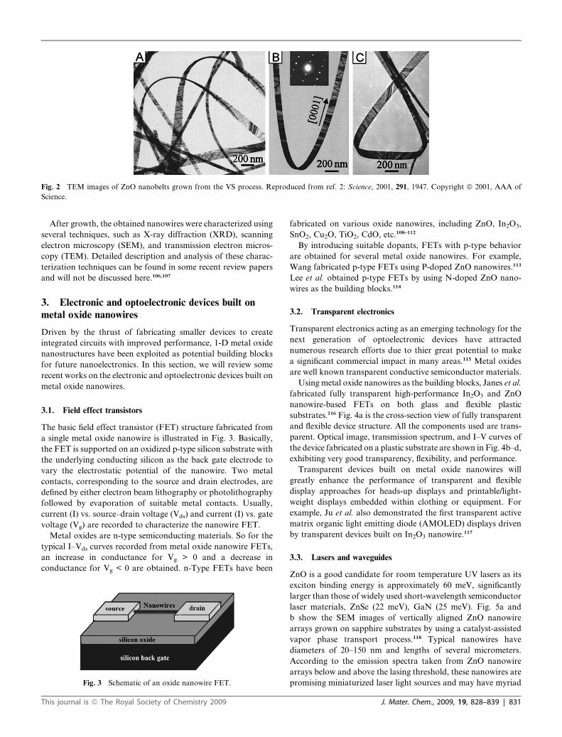
APPLICATION www.rsc.org/materials | Journal of Materials Chemistry
Devices and chemical sensing applications of metal oxide nanowires†
Guozhen Shen,* Po-Chiang Chen, Koungmin Ryu and Chongwu Zhou*
Received 22nd September 2008, Accepted 21st October 2008
First published as an Advance Article on the web 20th November 2008
DOI: 10.1039/b816543b
Metal oxide nanowires, with special physical properties, are ideal building blocks for a wide range of
nanoscale electronics, optoelectronics, and chemical sensing devices. This article will describe the state-
of-the-art research activities in metal oxide nanowire applications. This paper consists of three main
sections categorized by metal oxide nanowire synthesis, electronic and optoelectronic devices
applications, and chemical sensing applications. Finally, we will conclude this review with some
perspectives and outlook on the future developments in the metal oxide nanowire research area.
1. Introduction
Due to their special shapes, compositions, chemical and physical
properties, one-dimensional (1-D) metal oxide nanostructures
are the focus of current research efforts in nanotechnology since
they are the commonest minerals in the earth. 1-D metal oxide
nanostructures have now been widely used in many areas, such as
tro-optical and electro-chromic devices.1–5 Intensive studies have
been carried out on the synthesis of metal oxide nanowires as well
as the exploration of their novel properties. For example, 1-D
ZnO nanostructures with many different shapes, such as nano-
wires, nanobelts, nanotubes, nanorings, and nanosprings, have
been prepared using many synthesis methods. High-performance
chemical sensors have been fabricated on SnO2, ZnO, and In2O3
nanowires due to their large surface area to volume ratio.
Dr Guozhen Shen
Dr Guozhen Shen received his
Ph.D. degree in Chemistry from
University of Science and Tech-
nology of China in 2003. He
conducted his postdoctoral
research at Hanyang University,
Korea in 2004 and then joined
National Institute for Materials
Science, Japan as a visiting
researcher. Currently, he is
a research scientist in University
of Southern California. He is the
author or co-author of more
than 100 research articles and 5
book chapters. His most recent
research interests include the synthesis and characterization of one-
dimensional nanostructures and their device applications in elec-
tronics and optoelectronics.
Department of Electrical Engineering, University of Southern California,Los Angeles, CA 90089, USA. E-mail: [email protected]; [email protected]; [email protected]; Fax: +1 213 821 4208; Tel: +1 213 821 4208
† This paper is part of a Journal of Materials Chemistry theme issue onNanotubes and Nanowires. Guest editor: Z. L. Wang.
828 | J. Mater. Chem., 2009, 19, 828–839
This article will provide a comprehensive review of the state-
of-the-art research activities focused on devices and chemical
sensing applications of metal oxide nanowires, and can be
divided into three main sections. The first section briefly intro-
duces two synthesis strategies, which include top-down
approaches and bottom-up approaches, with the focus on
bottom-up approaches, for the synthesis of metal oxide nano-
wires. Next, some important electronic and optoelectronic
devices built on metal oxide nanowires are presented, which
include field-effect transistors (FETs), transparent electronics,
lasers and waveguide, nanogenerators, solar cells and photo-
catalysts, and field nanoemitters. In the third part, we will discuss
recent developments in the chemical sensing area of metal oxide
nanowires. The review will then conclude with some perspectives
and outlook on the future developments in the metal oxide
nanowire research area.
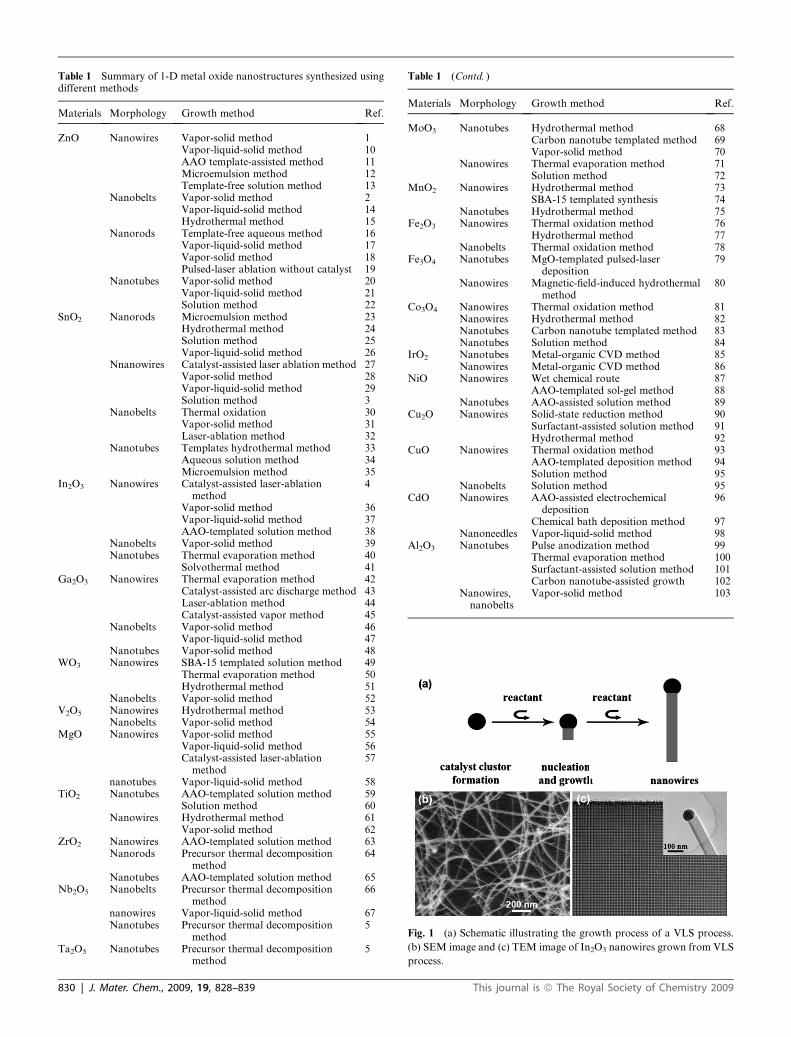
2. Synthesis of metal oxide nanowires
Till now, many methods have been developed to synthesize 1-D
metal oxide nanostructures. Basically, they can be described as
two different types: the ‘‘top-down’’ approaches and the
‘‘bottom-up’’ approaches. In this section, we will briefly discuss
Po-Chiang Chen
Po-Chiang Chen holds a B.S.
degree in Physics and a M.S. in
Optoelectronics. He is currently
working toward a Ph.D. degree
in Chemical Engineering and
Materials Science at the
University of Southern Cal-
ifornia. His research focus is on
the device applications based on
1-D nanomaterials, including
chemical sensors, transparent
electronics, and energy conver-
sion and storage devices.
This journal is ª The Royal Society of Chemistry 2009
In FET based chemical sensors, Fan et al. studied oxygen and
NO2 adsorption on the ZnO nanowire surface by using indi-
vidual ZnO nanowire field-effect transistors.177 The results of
sensing experiments can be observed in Fig. 11. A considerable
variation of conductance was observed when the device was
exposed to oxygen or NO2. In addition, an electrical potential to
the back gate electrode was applied, which could help to adjust
the sensitivity range of the device or initialize the device
completely before exposure to chemicals. This can be attributed
to the fact that the Fermi level within the nanowire band gap was
manipulated by applying an external gate voltage. In addition,
a ZnO chemical sensor was fully refreshed by applying a high
negative gate bias of 60 V as shown in Fig. 11.
Fig. 12 Principal component analysis (PCA) scores and loading plots of
a chemical sensor array composed of four different nanostructure
materials.
4.2. Optical and QCM based chemical sensors
With the novel characterization of contactless devices, recently
several research groups executed chemical sensing experiments
836 | J. Mater. Chem., 2009, 19, 828–839
based on metal oxide nanowire PL chemical sensors, such as
SnO2, and ZnO, etc.197,198 After exposure to chemicals, the
quenching of PL was observed.199 Although the microscopic
mechanisms are still not clear, the quenching is thought to be
related to the change of the oxidation state of the nanowire
surface before and after chemical exposure.197 In addition, the
sensing response time and recovery time are fast (merely a few
seconds), comparable with the response times of most electrical
based chemical sensors. For the QCM based sensor, it is thought
to be a mass-sensitive sensor, which can detect the change of
mass on a sensing layer. The mass of the sensing layer varies due
to the chemical reactions, adsorption, and deposition happening
above the surface of the sensing layer, while the sensor is exposed
to chemicals. QCM based sensors are also contactless devices.200
4.3. Electronic noses
The idea of electronic noses was inspired by the mechanisms of
human olfaction. In general, basic elements of an electronic nose
system include an ‘‘odour’’ sensor array, a data pre-processor,
and a pattern recognition (PARC) engine.201 There are several
methods to approach this goal, one is to make a chemical sensor
array with different nanostructured materials and the other is to
make a sensor chip with different material geometric properties
and temperature gradients (KAMINA technology). Kolmakov
et al. adapted this idea and fabricated a KAMINA sensor chip
composed of SnO2 nanowires with different nanowire densities,
which exhibited good selectivity for several chemicals.202 The
achievement not only successfully solved the ‘‘selectivity’’ issue
but also brought nanotechnology a step closer to practical
application.
Very recently, we developed a new template built with four
different semiconducting nanostructures: In2O3 nanowires, SnO2
nanowires, ZnO nanowires and single-wall C nanotubes (SWNT)
as electronic noses to detect different chemicals (Fig. 12 inset).203
n-Type metal oxide nanowires and p-type C nanotubes provide
one discrimination factor. The integrated micromachined hot
plate enables individual and accurate temperature control of
each sensor, which provides the second discrimination factor.
This journal is ª The Royal Society of Chemistry 2009
When this sensor array was exposed to different chemicals, good
selectivity was obtained to build up an interesting ‘‘smell-print’’
library of the detected chemicals (Fig. 12).
5. Summary
In summary, we provide a comprehensive review of the state-of-
the-art research activities focused on devices and chemical sensing
applications of metal oxide nanowires. The fascinating achieve-
ments, till now, towards the device applications of metal oxide
nanowires should inspire more and more research efforts to address
the remaining challenges in this interesting field. We tried to include
the most important topics in this review article. However, due to the
tremendous research effort and space limitations, this article is
unable to list all the exciting works reported in this field.
Although comprehensive efforts have been made towards the
synthesis of high quality metal oxide nanowires, there is still
plenty of room left unexploited. We believe that future work in
the nanowire synthesis direction should continue to focus on
generating high quality and large quantity metal oxide nanowires
in more controlled, predictable and simple ways. One key issue of
metal oxide nanowires is the growth of p-type metal oxide
nanowires or the formation of intra-nanowire p-n junctions,
which will significantly advance and widen the device application
of metal oxide nanowires.
One interesting area in the metal oxide nanowire based
chemical sensors area is still the development of high quality 1-D
metal oxide nanostructures to be used as chemical sensing
elements. The sensing issues of extremely high sensitivity, selec-
tivity and stability should be resolved. Though some research
groups have successfully detected important chemicals using 1-D
metal oxide nanostructures, the selectivity is still quite low.
Furthermore, other potential and interesting areas which need
further exploration may be the detection of very small amounts
of nerve agents such as sarin and soman, or of explosive chem-
icals for personal health and human security applications.
References
1 P. D. Yang, H. Q. Yan, S. Mao, R. Russo, J. Johnson, R. Saykally,N. Morris, J. Pham, R. R. He and H. J. Cho, Adv. Funct. Mater.,2002, 12, 323.
2 Z. W. Pan, Z. R. Dai and Z. L. Wang, Science, 2001, 291, 1947.3 Y. L. Wang, X. C. Jiang and Y. Xia, J. Am. Chem. Soc., 2003, 125,
16176.4 C. Li, D. Zhang, S. Han, X. Liu, T. Tang and C. Zhou, Adv. Mater.,
2003, 15, 143.5 Y. Kobayashi, H. Hata, M. Salama and T. E. Mallouk, Nano Lett.,
2007, 7, 2142.6 H. W. Ra, K. S. Choi, J. H. Kim, Y. B. Hahn and Y. H. Im, Small,
2008, 4, 1105.7 F. L. Zhang, T. Nyberg and O. Inganas, Nano Lett., 2002, 2, 1373.8 X. Duan and C. M. Lieber, Adv. Mater., 2000, 12, 298.9 C. M. Lieber, MRS Bull., 2003, 28, 486.
10 Y. W. Wang, L. D. Zhang, G. Z. Wang, X. S. Peng, Z. Q. Chu andC. H. Liang, J. Cryst. Growth, 2002, 234, 171.
11 Y. Li, G. W. Meng, L. D. Zhang and F. Phillipp, Appl. Phys. Lett.,2000, 76, 2011.
12 H. Zhang, D. Yang, Y. J. Ji, X. Y. Ma, J. Xu and D. L. Que, J. Phys.Chem. B, 2004, 108, 3955.
13 H. Zhang, D. R. Yang, X. Y. Ma and D. L. Que, J. Phys. Chem. B,2005, 109, 17055.
14 Y. Ding, P. X. Gao and Z. L. Wang, J. Am. Chem. Soc., 2004, 126,2066.
This journal is ª The Royal Society of Chemistry 2009
15 X. Y. Zhang, J. Y. Dai, H. C. Ong, N. Wang, H. L. W. Chan andC. L. Choy, Chem. Phys. Lett., 2004, 393, 17.
16 L. Vayssieres, Adv. Mater., 2003, 15, 464.17 P. X. Gao and Z. L. Wang, J. Phys. Chem. B, 2004, 108, 7534.18 Z. L. Wang, J. Nanosci. Nanotechnl., 2008, 8, 27.19 A. B. Hartanto, X. Ning, Y. Nakata and T. Okada, Appl. Phys. A,
2004, 78, 299.20 Y. J. Xing, Z. H. Xi, Z. Q. Xue, X. D. Zhang, J. H. Song,
R. M. Wang, J. Xu, Y. Song, S. L. Zhang and D. P. Yu, Appl.Phys. Lett., 2003, 83, 1689.
21 X. Kong, X. M. Sun, X. L. Li and Y. D. Li, Mater. Chem. Phys.,2003, 82, 997.
22 Y. Sun, G. M. Fuge, N. A. Fox, D. J. Riley and M. N. R. Ashfold,Adv. Mater., 2005, 17, 2477.
23 Y. K. Liu, C. L. Zheng, W. Z. Wang, C. R. Yin and G. H. Wang,Adv. Mater., 2001, 13, 1883.
24 D. F. Zhang, L. D. Sun, J. L. Yin and C. H. Yan, Adv. Mater., 2003,15, 1022.
25 B. Cheng, J. M. Russell, W. S. Shi, L. Zhang and E. T. Samulski,J. Am. Chem. Soc., 2004, 126, 5972.
26 J. H. He, T. H. Wu, C. L. Hsin, K. M. Li, L. J. Chen, Y. L. Chueh,L. J. Chou and Z. L. Wang, Small, 2006, 2, 116.
27 Z. Liu, D. Zhang, S. Han, C. Li, T. Tang, W. Jin, X. Liu, B. Lei andC. Zhou, Adv. Mater., 2003, 15, 1754.
28 S. Luo, P. K. Chu, W. Liu, M. Zhang and C. L. Lin, Appl. Phys.Lett., 2006, 88, 183112.
29 Y. Chen, X. Cui, K. Zhang, D. Pan, S. Zhang, B. Wang andJ. G. Hou, Chem. Phys. Lett., 2003, 369, 16.
30 S. Sun, G. W. Meng, G. Zhang, T. Gao, B. Geng, L. D. Zhang andJ. Zuo, Chem. Phys. Lett., 2003, 376, 103.
31 J. Duan, S. Yang, H. Liu, J. Gong, H. Huang, X. Zhao, R. Zhangand Y. Du, J. Am. Chem. Soc., 2005, 107, 6180.
32 J. Hu, Y. Bando, Q. Liu and D. Golberg, Adv. Funct. Mater., 2003,13, 493.
33 B. Liu and H. C. Zeng, J. Phys. Chem. B, 2004, 108, 5867.34 N. Du, H. Zhang, B. Chen, X. Ma and D. R. Yang, Chem. Commun.,
2008, 3028.35 N. Wang, X. Cao and L. Guo, J. Phys. Chem. C, 2008, 112, 12616.36 X. S. Peng, G. W. Meng, J. Zhang, X. F. Wang, Y. W. Wang,
C. Z. Wang and L. D. Zhang, J. Mater. Chem., 2002, 12, 1602.37 J. Zhang, X. Qing, F. H. Jiang and Z. H. Dai, Chem. Phys. Lett.,
2003, 371, 311.38 H. Q. Cao, X. Q. Qiu, Y. Liang, Q. Zhu and M. Zhao, Appl. Phys.
Lett., 2003, 83, 761.39 X. Y. Kong and Z. L. Wang, Solid State Commun., 2003, 128, 1.40 Y. Li, Y. Bando and D. Golberg, Adv. Mater., 2003, 15, 581.41 C. Chen, D. Chen, X. Jiao and C. Qang, Chem. Commun., 2006,
4632.42 H. Zhang, Y. Kong, Y. Wang, X. Du, Z. Bai, J. Wang, D. P. Yu,
Y. Ding, Q. Hang and S. Feng, Solid State Commun., 1999, 109, 677.43 Y. C. Choi, W. S. Kim, Y. S. Park, S. M. Lee, D. J. Bae, Y. H. Lee,
G. S. Park, W. B. Choi, N. S. Lee and J. M. Kim, Adv. Mater., 2000,12, 746.
44 J. Hu, Q. Li, X. Meng, C. S. Lee and S. T. Lee, J. Phys. Chem. B,2002, 106, 9536.
45 K. W. Chang and J. J. Wu, Appl. Phys. A, 2003, 76, 629.46 B. Geng, L. D. Zhang, G. W. Meng, T. Xie, X. Peng and Y. Lin,
J. Cryst. Growth, 2003, 259, 291.47 J. Zhagn, F. H. Jiang, Y. Yang and J. Li, J. Phys. Chem. B, 2005,
109, 13143.48 N. Gong, M. Lu, C. Y. Wang, Y. Chen and L. J. Chen, Appl. Phys.
Lett., 2008, 92, 073101.49 K. Zhu, H. He, S. Xie, X. Zhang, W. Zhou, S. Jin and B. Yue, Chem.
Phys. Lett., 2003, 377, 317.50 Y. Baek and K. Yong, J. Phys. Chem. C, 2007, 111, 1213.51 X. Song, Y. Zheng, E. Yang and Y. Wang, Mater. Lett., 2007, 61,
3904.52 Y. Li, Y. Bando, D. Golberg and K. Kurashima, Chem. Phys. Lett.,
2003, 367, 214.53 F. Zhou, X. Zhao, Y. Liu, C. Yuan and L. Li, Eur. J. Inorg. Chem.,
2008, 16, 2506.54 C. K. Chan, H. Peng, R. D. Twesten, K. Jarausch, X. F. Zhang and
Y. Cui, Nano Lett., 2007, 7, 490.55 Y. Yin, G. Zhang and Y. N. Xia, Adv. Funct. Mater., 2002, 12, 293.56 H. W. Kim and S. H. Shim, Chem. Phys. Lett., 2006, 422, 165.
J. Mater. Chem., 2009, 19, 828–839 | 837
57 K. Nagashima, T. Yanagida, H. Tanaka and T. Kawai, J. Appl.Phys., 2007, 101, 124304.
58 J. H. Zhan, Y. Bando, J. Hu and D. Golberg, Inorg. Chem., 2004, 43,2462.
59 H. Imai, Y. Takei, K. Shimizu, M. Matsuda and H. Hirashima,J. Mater. Chem., 1999, 9, 2971.
60 S. Liu, L. Gan, L. Liu, W. Zhang and H. Zeng, Chem. Mater., 2002,14, 1391.
61 Y. Zhang, G. Li, Y. Jin, Y. Zhang, J. Zhang and L. D. Zhang, Chem.Phys. Lett., 2002, 365, 300.
62 J. M. Wu, H. C. Shih and W. T. Wu, Chem. Phys. Lett., 2005, 413,490.
63 H. Cao, X. Qiu, B. Luo, Y. Liang, Y. Zhang, R. Tan, M. Zhao andQ. Zhu, Adv. Funct. Mater., 2004, 14, 243.
64 L. Li and W. Z. Wang, Solid State Commun., 2003, 127, 639.65 C. Dae, S. Kim, B. Ahn, J. Kim, M. Sung and H. Shin, J. Mater.
Chem., 2008, 18, 1362.66 M. Wei, Z. M. Qi, M. Ichihara and H. Zhou, Acta Mater., 2008, 56,
2488.67 B. Varghese, S. C. Haur and C. T. Lim, J. Phys. Chem. C, 2008, 112,
10008.68 S. Hu and X. Wang, J. Am. Chem. Soc., 2008, 130, 8126.69 B. C. Satishkumar, A. Govindaraj, E. M. Vogl, L. Basumallick and
C. N. R. Rao, J. Mater. Res., 1997, 12, 604.70 Y. Li and Y. Bando, Chem. Phys. Lett., 2002, 364, 484.71 J. Zhou, S. Deng, N. S. Xu, J. Chen and J. She, Appl. Phys. Lett.,
2003, 83, 2653.72 B. Qi, X. Ni, D. Li and H. Zheng, Chem. Lett., 2008, 37, 336.73 X. Wang and Y. D. Li, J. Am. Chem. Soc., 2002, 124, 2880.74 M. Imperor-Clerc, D. Bazin, M. D. Appay, P. Beaunier and
A. Davidson, Chem. Mater., 2004, 16, 1813.75 D. Zheng, S. X. Sun, W. Fan, H. Yu, C. Fan, G. Cao, Z. Yin and
X. Song, J. Phys. Chem. B, 2005, 109, 16439.76 Y. Fu, J. Chen and H. Zhang, Chem. Phys. Lett., 2001, 350, 491.77 Y. Xiong, Y. Xie, Z. Li, R. Zhang, J. Yang and C. Wu, New
J. Chem., 2003, 27, 588.78 X. Wen, S. Wang, Y. Ding, Z. L. Wang and S. Yang, J. Phys. Chem.
B, 2005, 109, 215.79 Z. Liu, D. Zhang, S. Han, C. Li, B. Lei, W. Lu, J. Fang and C. Zhou,
J. Am. Chem. Soc., 2005, 127, 6.80 J. Wang, Q. W. Chen, C. Zeng and B. Y. Hou, Adv. Mater., 2004, 16,
137.81 Z. Dong, Y. Y. Fu, Q. Han, Y. Xu and H. Zhang, J. Phys. Chem. C,
2007, 111, 18475.82 H. Zhang, J. Wu, C. Zhai, X. Ma, N. Du, J. Tu and D. R. Yang,
Nanotechnology, 2008, 19, 035711.83 N. Du, H. Zhang, B. Chen, J. Wu, X. Ma, Z. Liu, Y. Zhang,
D. Yang, X. Huang and J. Tu, Adv. Mater., 2007, 19, 4505.84 X. W. Lou, D. Deng, J. Y. Lee, J. Feng and L. A. Archer, Adv.
Mater., 2008, 20, 258.85 R. S. Chen, Y. S. Huang, D. S. Tsai, S. Chattopadhyay, C. T. Wu,
Z. H. Lan and K. H. Chen, Chem. Mater., 2004, 16, 2457.86 Y. L. Chen, C. C. Hsu, Y. H. Song, Y. Chi, A. J. Carty, S. M. Peng
and G. H. Lee, Chem. Vapor. Dep., 2006, 12, 442.87 C. K. Xu, K. Q. Hong, S. Liu, G. H. Wang and X. N. Zhao, J. Cryst.
Growth, 2003, 255, 308.88 Q. Yang, J. Sha, X. Y. Ma and D. R. Yang, Mater. Lett., 2005, 59,
1967.89 C. S. Shi, G. Q. Wang, N. Q. Zhao, X. W. Du and J. J. Li, Chem.
Phys. Lett., 2008, 454, 75.90 W. Z. Wang, G. H. Wang, X. S. Wang, Y. J. Zhan, Y. K. Liu and
C. L. Zheng, Adv. Mater., 2002, 14, 67.91 Y. J. Xiong, Z. Q. Li, R. Zhang, Y. Xie, J. Yang and C. Z. Wu,
J. Phys. Chem. B, 2003, 107, 3697.92 Y. W. Tan, X. Y. Xue, Q. Peng, H. Zhao, T. H. Wang and Y. D. Li,
Nano Lett., 2007, 7, 3723.93 X. C. Jiang, T. Herricks and Y. N. Xia, Nano Lett., 2002, 2,
1333.94 E. Ko, J. Choi, K. Okamoto, Y. Tak and J. Lee, ChemPhysChem.,
2006, 7, 1505.95 G. H. Du and G. Van Tendeloo, Chem. Phys. Lett., 2004, 393, 64.96 X. S. Peng, X. F. Wang, Y. W. Wang, C. Z. Wang, G. W. Meng and
L. D. Zhang, J. Phys. D., 2002, 35, L101.97 D. S. Dhawale, A. M. More, S. S. Latthe, K. Y. Rajpure and
C. D. Lokhande, Appl. Surf. Sci., 2008, 254, 3269.
838 | J. Mater. Chem., 2009, 19, 828–839
98 X. Liu, C. Li, S. Han, J. Han and C. Zhou, Appl. Phys. Lett., 2003,82, 1950.
99 W. Lee, R. Scholz and U. Gosele, Nano Lett., 2008, 8, 2155.100 Y. B. Li, Y. Bando and D. Golberg, Adv. Mater., 2005, 17, 1401.101 D. B. Kuang, Y. P. Fang, H. Q. Liu, C. Frommen and D. Fenske,
J. Mater. Chem., 2003, 13, 660.102 H. Ogihara, M. Sadakane, Y. Nodasaka and W. Ueda, Chem.
Mater., 2006, 18, 4981.103 X. S. Peng, L. D. Zhang, G. W. Meng, X. F. Wang, Y. W. Wang,
C. Z. Wang and G. S. Wu, J. Phys. Chem. B, 2002, 106, 11163.104 R. S. Wagner and W. C. Ellis, Appl. Phys. Lett., 1964, 4, 89.105 T. J. Trentler, K. M. Hickman, S. C. Goel, A. M. Viano,
P. C. Gibbons and W. E. Buhro, Science, 1995, 270, 1791.106 J. G. Lu, P. Chang and Z. Fan, Mater. Sci. Eng. R, 2006, 52, 49.107 Y. Ding and Z. L. Wang, J. Phys. Chem. B, 2004, 108, 12280.108 P. Chang, Z. Fan, D. Wang, W. Tseng, W. Chiou, J. Hong and
J. G. Lu, Chem. Mater., 2004, 16, 5133.109 C. Li, D. Zhang, S. Han, X. Liu, T. Tang and C. Zhou, Adv. Mater.,
2003, 15, 143.110 Z. Liu, D. Zhang, S. Han, C. Li, T. Tang, W. Jin, X. Liu, B. Lei and
C. Zhou, Adv. Mater., 2003, 15, 1754.111 X. Liu, C. Li, S. Han, J. Han and C. Zhou, Appl. Phys. Lett., 2003,
82, 1950.112 Y. Tan, X. Xue, Q. Peng, H. Zhao, T. Wang and Y. Li, Nano Lett.,
2007, 7, 3723.113 B. Xiang, P. Wei, X. Zhang, S. A. Dayeh, D. P. R. Aplin, C. Soci,
D. Yu and D. Wang, Nano Lett., 2007, 7, 323.114 G. D. Yuan, W. J. Zhang, J. Jie, X. Fan, J. A. Zapien, Y. H. Leung,
L. B. Luo, P. F. Wang, C. S. Lee and S. T. Lee, Nano Lett., 2008, 8,2591.
115 K. Nomura, H. Ohta, K. Ueda, T. Kamiya, M. Hirano andH. Hosono, Science, 2003, 300, 1269.
116 S. Ju, A. Facchetti, Y. Xuan, J. Liu, F. Ishikawa, P. Ye, C. Zhou,T. J. Marks and D. B. Janes, Nat. Nanotech., 2007, 2, 378.
117 S. Ju, J. Li, J. Liu, P. Chen, Y. Ha, F. Ishikawa, H. Chang, C. Zhou,A. Facchetti, D. B. Janes and T. J. Marks, Nano Lett., 2008, 8, 997.
118 M. Huang, S. Mao, H. Feick, H. Yan, Y. Wu, H. Kind, E. Weber,R. Russo and P. Yang, Science, 2001, 292, 1897.
119 J. Johnson, H. Yan, R. Schaller, L. Haber, R. Saykally and P. Yang,J. Phys. Chem. B, 2001, 105, 11387.
120 H. Kind, H. Yan, M. Law, B. Messer and P. Yang, Adv. Mater.,2002, 14, 158.
121 H. Yan, R. He, J. Johnson, M. Law, R. J. Saykally and P. Yang,J. Am. Chem. Soc., 2003, 125, 4728.
122 M. Law, D. Sirbuly, J. Johnson, J. Goldberger, R. Saykally andP. Yang, Science, 2004, 305, 1269.
123 Z. L. Wang and J. Song, Science, 2006, 312, 242.124 X. Wang, J. Song, J. Liu and Z. L. Wang, Science, 2007, 316, 102.125 Y. Qin, X. Wang and Z. L. Wang, Nature, 2008, 451, 809.126 X. Wang, J. Zhou, J. Song, J. Liu, N. Xu and Z. L. Wang, Nano
Lett., 2006, 6, 2768.127 J. H. He, C. L. Hsin, J. Liu, L. J. Chen and Z. L. Wang, Adv. Mater.,
2007, 19, 781.128 M. Law, L. E. Greene, J. C. Johnson, R. Saykally and P. Yang,
Nature Mater., 2005, 4, 455.129 J. T. Liu, F. M. Wang, S. Isoda and M. Adachi, Chem. Lett., 2005,
34, 1506.130 L. Greene, M. Law, B. Yuhas and P. Yang, J. Phys. Chem. C, 2007,
111, 18451.131 M. Law, L. Greene, A. Radenovic, T. Kuykendall, J. Liphardt and
P. Yang, J. Phys. Chem. B, 2006, 110, 22652.132 S. Anandan, X. Wen and S. Yang, Mater. Chem. Phys., 2005, 93, 35.133 K. Wang, J. Chen, W. Zhou, Y. Zhang, Y. Yan, J. Pern and
A. Mascarenhas, Adv. Mater., 2008, 20, 3248.134 A. Fujishimam and K. Honda, Nature, 1972, 238, 37.135 M. R. Hoffmann, S. T. Martin, W. Choi and D. W. Bahnemann,
Chem. Rev., 1995, 95, 69.136 H. Choi, A. C. Sofranko and D. D. Dionysiou, Adv. Funct. Mater.,
2006, 16, 1067.137 S. J. Hwang, C. Petucci and D. Raftery, J. Am. Chem. Soc., 1997,
119, 7877.138 C. Wu, L. Lei, X. Zhu, J. Yang and Y. Xie, Small, 2007, 9, 1518.139 Y. Mao and S. S. Wong, J. Am. Chem. Soc., 2006, 128, 8217.140 G. Wang, W. Lu, J. Li, J. Choi, Y. Jeong, S. Y. Choi, J. B. Park,
M. K. Ryu and K. Lee, Small, 2006, 2, 1436.
This journal is ª The Royal Society of Chemistry 2009
141 Y. Wang, Z. Zhang, Y. Zhu, Z. Li, R. Vajtai, L. Ci andP. M. Ajayan, ACS Nano, 2008, 2, 1492.
142 D. Chen and J. Ye, Chem. Mater., 2007, 19, 4585.143 Y. Yu and D. Xu, Appl. Cata. B, 2007, 73, 166.144 T. J. Kuo, C. N. Lin, C. L. Kuo and M. H. Huang, Chem. Mater.,
2007, 19, 5143.145 L. Zhou, W. Wang, L. Zhang, H. Xu and W. Zhu, J. Phys. Chem. C,
2007, 111, 13659.146 C. J. Lee, T. J. Lee, S. C. Lyu, Y. Zhang, H. Ruh and H. J. Lee, Appl.
Phys. Lett., 2002, 81, 3648.147 H. Ham, G. Z. Shen, J. H. Cho, T. J. Lee, S. H. Seo and C. J. Lee,
Chem. Phys. Lett., 2005, 404, 69.148 G. Z. Shen, Y. Bando, B. D. Liu, D. Golberg and C. J. Lee, Adv.
Funct. Mater., 2006, 16, 410.149 Y. K. Tseng, C. J. Huang, H. M. Cheng, I. N. Lin, K. S. Liu and
I. C. Chen, Adv. Funct. Mater., 2003, 13, 811.150 C. X. Xu and X. W. Sun, Appl. Phys. Lett., 2003, 83, 3806.151 Y. B. Li, Y. Bando and D. Golberg, Appl. Phys. Lett., 2004, 84,
3603.152 D. Banerjee, S. H. Jo and Z. F. Ren, Adv. Mater., 2004, 16, 2028.153 Y. H. Baek and K. J. Yong, J. Phys. Chem. C, 2007, 111, 1213.154 Y. B. Li, Y. Bando and D. Golberg, Adv. Mater., 2003, 15, 1294;
J. Zhou, L. Gong, S. Z. Deng, J. Chen, J. C. She, N. S. Xu,R. S. Yang and Z. L. Wang, Appl. Phys. Lett., 2005, 87, 223108.
155 M. T. Chang, L. J. Chou, Y. L. Chueh, Y. C. Lee, C. H. Hsieh,C. D. Chen, Y. W. Lan and L. J. Chen, Small, 2007, 3, 658.
156 J. G. Liu, Z. J. Zhang, Y. Zhao, X. Su, S. Liu and E. G. Wang,Small, 2005, 1, 310.
157 C. S. Hsieh, D. S. Tsai, R. S. Chen and Y. S. Huang, Appl. Phys.Lett., 2004, 85, 3860.
158 C. L. Cheng, Y. F. Chen, R. S. Chen and Y. S. Huang, Appl. Phys.Lett., 2005, 86, 103104.
159 Y. W. Zhu, A. M. Moo, T. Yu, X. J. Xu, X. Y. Gao, Y. J. Liu,C. T. Lim, Z. X. Shen, C. K. Ong, A. T. S. Wee, J. T. L. Thongand C. H. Sow, Chem. Phys. Lett., 2006, 419, 458.
160 J. Chen, S. Z. Deng, N. S. Xu, W. X. Zhang, X. G. Wen andS. H. Yang, Appl. Phys. Lett., 2003, 83, 746.
161 J. M. Wu, H. C. Shih and W. T. Wu, Chem. Phys. Lett., 2005, 413,490.
162 J. H. He, T. H. Wu, C. L. Hsin, K. M. Li, L. J. Chen, Y. L. Chueh,L. J. Chou and Z. L. Wang, Small, 2006, 2, 116.
163 Y. J. Chen, Q. H. Li, Y. X. Liang, T. H. Wang, Q. Zhao andD. P. Yu, Appl. Phys. Lett., 2004, 85, 5682.
164 S. Q. Li, Y. X. Liang and T. H. Wang, Appl. Phys. Lett., 2006, 88,053107.
165 S. Kar, S. Chakrabarti and S. Chaudhuri, Nanotechnology, 2006, 17,3058.
166 D. Zhang, Z. Liu, C. Li, T. Tang, X. Liu, S. Han, B. Lei andC. Zhou, Nano Lett., 2004, 4, 1919.
167 C. Li, D. Zhang, X. Liu, S. Han, T. Tang, J. Han and C. Zhou, Appl.Phys. Lett., 2003, 82, 1613.
168 C. Li, D. Zhang, B. Lei, S. Han, X. Liu and C. Zhou, J. Phys. Chem.B, 2003, 107, 12451.
169 C. Baratto, E. Comini, G. Faglia, G. Sberveglieri, M. Zha andA. Zappettini, Sens. Actuators B, 2005, 109, 2.
170 X. Y. Xue, Y. J. Chen, Y. G. Liu, S. L. Shi, Y. G. Wang andT. H. Wang, Appl. Phys. Lett., 2006, 88, 201907.
171 Y. Zhang, A. Kolmakov, S. Chretien, H. Metiu and M. Moskovits,Nano Lett., 2004, 3, 403.
172 A. Kolmakov, Y. Zhang, G. Cheng and M. Moskovits, Adv. Mater.,2003, 15, 997.
This journal is ª The Royal Society of Chemistry 2009
173 F. Hernandez-Ramirez, A. Tarancon, O. Casals, J. Arbiol,A. Romano-Rodriguez and J. R. Morante, Sens. Actuators B,2007, 121, 3.
174 X. Y. Xue, Y. J. Chen, Y. G. Liu, S. L. Shi, Y. G. Wang andT. H. Wang, Appl. Phys. Lett., 2006, 88, 201907.
175 Q. Wan and T. H. Wang, Chem. Commun., 2005, 3841.176 N. S. Ramgir, I. S. Mulla and K. P. Vijayamohanan, Sens. Actuators
B, 2005, 107, 708.177 Z. Fan and J. G. Lu, Appl. Phys. Lett., 2005, 86, 123510.178 Q. Wan, Q. H. Li, Y. J. Chen, T. H. Wang, X. L. He and J. P. Li,
Appl. Phys. Lett., 2004, 85, 6389.179 T.-J. Hsueh, C.-L. Hsu, S.-J. Chang and I. C. Chen, Sens. Actuators
B, 2007, 126, 473.180 Z. Fan, D. Wang, P. Chang, W.-Y. Tseng and J. G. Lu, Appl. Phys.
Lett., 2004, 85, 5923.181 X. Wang, J. Zhang and Z. Zhu, Appl. Surf. Sci., 2006, 252, 2404.182 B. S. Kang, Y. W. Heo, L. C. Tien, D. P. Norton, R. Ren, B. P. Gila
and S. J. Pearton, Appl. Phys. A, 2005, 80, 1029.183 H. T. Wang, B. S. Kang, F. Ren, P. W. Sadic, D. P. Norton,
S. J. Pearton and J. Lin, Appl. Phys. A, 2005, 81, 1117.184 T.-J. Hsueh, Y.-W. Chen, S.-J. Chang, S.-F. Wang, C.-L. Hus, Y.-
R. Lin, T.-S. Lin and I. C. Chen, Sens. Actuators B, 2007, 125, 498.185 H. T. Wang, B. S. Kang, F. Ren, L. C. Tien, P. W. Sadik,
D. P. Norton and S. J. Pearton, Appl. Phys. Lett., 2005, 86, 243503.186 L. C. Tien, H. T. Wang, B. S. Kang, F. Ren, P. W. Sadik,
D. P. Norton, S. J. Pearton and J. Lin, Electrochem and SolidState Lett., 2005, 9, G230.
187 Y. Huang, S. Yue, Z. Wang, Q. Wang, C. Shi, Z. Xu, X. D. Bai,C. Tang and C. Gu, J. Phys. Chem. B, 2006, 110, 796.
188 M. F. Yu and M. Z. Atashbar, IEEE Sensors, 2005, 5, 20.189 A. Ponzoni, E. Comini, G. Sbergeglieli, J. Zhou, S. Z. Deng,
N. S. Xu, Y. Ding and Z. L. Wang, Appl. Phys. Lett., 2006, 88,203101.
190 Z. Liu, T. Yamazki, Y. Shen and T. Kikuta, Appl. Phys. Lett., 2007,90, 173119.
191 H. Y. Yu, B. H. Kang, U. H. Pi, C. W. Park and S.-Y. Choi, VAppl.Phys. Lett., 2005, 86, 253102.
192 I. Raible, M. Burghard, U. Schlecht, A. Yasuda and T. Vossever,Sens. Actuators B, 2005, 106, 730.
193 X. Y. Xue, Y. J. Chen, Y. G. Wang and T. H. Wang, Appl. Phys.Lett., 2005, 86, 233101.
194 X. Y. Xue, P. Feng, Y. G. Wang and T. H. Wang, Appl. Phys. Lett.,2007, 91, 022111.
195 C. Baratto, E. Comini, G. Faglia, G. Sberveglieri, M. Zha andA. Zappettini, Sens. Actuators B, 2005, 109, 2.
196 K. Ryu, D. Zhang and C. Zhou, Appl. Phys. Lett., 2008, 92, 93111.197 A. Setaro, A. Bismuto, S. Lettieri, P. Maddalena, E. Comini,
S. Bianchi, C. Baratto and Sberveglieri, Sens. Actuators B, 2008,130, 391.
198 E. Comini, C. Baratto, G. Faglia, M. Ferroni and G. Sberveglieri,J. Phys. D. Appl. Phys., 2007, 40, 7255.
199 G. Faglia, C. Baratto, G. Sberveglieri, M. Zha and A. Zappettini,Appl. Phys. Lett., 2005, 86, 011923.
200 X. Zhou, J. Zhang, T. Jiang, X. Wang and Z. Zhu, Sens. ActuatorsA, 2007, 135, 209.
201 M. A. Craven, J. G. Gardner and P. N. Bartlett, Trends in AnalyticalChemistry, 1996, 15, 486.
202 V. V. Sysoev, J. Goschnick, T. Schneider, E. Strelcov andA. Kolmakov, Nano Lett., 2007, 7, 3182.
203 P. C. Chen, F. N. Ishikawa, H. K. Chang, K. Ryu, and C. Zhou,unpublished results.